US8729797B2 - Organic light emitting diode display and manufacturing method thereof - Google Patents

Organic light emitting diode display and manufacturing method thereof Download PDF

Info

Publication number
US8729797B2
US8729797B2 US13/302,321 US201113302321A US8729797B2 US 8729797 B2 US8729797 B2 US 8729797B2 US 201113302321 A US201113302321 A US 201113302321A US 8729797 B2 US8729797 B2 US 8729797B2
Authority
US
United States
Prior art keywords
functional
oligomer
layer
thin film
pixel
Prior art date
Legal status (The legal status is an assumption and is not a legal conclusion. Google has not performed a legal analysis and makes no representation as to the accuracy of the status listed.)
Active, expires
Application number
US13/302,321
Other versions
US20120256534A1 (en
Inventor
So-Young Lee
Yoon-Hyeung Cho
Min-Ho Oh
Byoung-Duk Lee
Yong-Tak Kim
Sang-Hwan Cho
Yun-Ah Chung
Seung-Yong Song
Jong-hyuk Lee
Current Assignee (The listed assignees may be inaccurate. Google has not performed a legal analysis and makes no representation or warranty as to the accuracy of the list.)
Samsung Display Co Ltd
Original Assignee
Samsung Display Co Ltd
Priority date (The priority date is an assumption and is not a legal conclusion. Google has not performed a legal analysis and makes no representation as to the accuracy of the date listed.)
Filing date
Publication date
Application filed by Samsung Display Co Ltd filed Critical Samsung Display Co Ltd
Assigned to SAMSUNG MOBILE DISPLAY CO., LTD. reassignment SAMSUNG MOBILE DISPLAY CO., LTD. ASSIGNMENT OF ASSIGNORS INTEREST (SEE DOCUMENT FOR DETAILS). Assignors: CHO, SANG-HWAN, CHO, YOON-HYEUNG, CHUNG, YUN-AH, KIM, YONG-TAK, LEE, BYOUNG-DUK, LEE, JONG-HYUK, LEE, SO-YOUNG, OH, MIN-HO, SONG, SEUNG-YONG
Assigned to SAMSUNG DISPLAY CO., LTD. reassignment SAMSUNG DISPLAY CO., LTD. MERGER (SEE DOCUMENT FOR DETAILS). Assignors: SAMSUNG MOBILE DISPLAY CO., LTD.
Publication of US20120256534A1 publication Critical patent/US20120256534A1/en
Application granted granted Critical
Publication of US8729797B2 publication Critical patent/US8729797B2/en
Active legal-status Critical Current
Adjusted expiration legal-status Critical

Links

Images

Classifications

    • BPERFORMING OPERATIONS; TRANSPORTING
    • B32LAYERED PRODUCTS
    • B32BLAYERED PRODUCTS, i.e. PRODUCTS BUILT-UP OF STRATA OF FLAT OR NON-FLAT, e.g. CELLULAR OR HONEYCOMB, FORM
    • B32B37/00Methods or apparatus for laminating, e.g. by curing or by ultrasonic bonding
    • B32B37/0007Methods or apparatus for laminating, e.g. by curing or by ultrasonic bonding involving treatment or provisions in order to avoid deformation or air inclusion, e.g. to improve surface quality
    • HELECTRICITY
    • H10SEMICONDUCTOR DEVICES; ELECTRIC SOLID-STATE DEVICES NOT OTHERWISE PROVIDED FOR
    • H10KORGANIC ELECTRIC SOLID-STATE DEVICES
    • H10K50/00Organic light-emitting devices
    • H10K50/80Constructional details
    • H10K50/84Passivation; Containers; Encapsulations
    • H10K50/844Encapsulations
    • BPERFORMING OPERATIONS; TRANSPORTING
    • B32LAYERED PRODUCTS
    • B32BLAYERED PRODUCTS, i.e. PRODUCTS BUILT-UP OF STRATA OF FLAT OR NON-FLAT, e.g. CELLULAR OR HONEYCOMB, FORM
    • B32B37/00Methods or apparatus for laminating, e.g. by curing or by ultrasonic bonding
    • B32B37/12Methods or apparatus for laminating, e.g. by curing or by ultrasonic bonding characterised by using adhesives
    • B32B37/1207Heat-activated adhesive
    • HELECTRICITY
    • H10SEMICONDUCTOR DEVICES; ELECTRIC SOLID-STATE DEVICES NOT OTHERWISE PROVIDED FOR
    • H10KORGANIC ELECTRIC SOLID-STATE DEVICES
    • H10K59/00Integrated devices, or assemblies of multiple devices, comprising at least one organic light-emitting element covered by group H10K50/00
    • H10K59/10OLED displays
    • H10K59/12Active-matrix OLED [AMOLED] displays
    • H10K59/1201Manufacture or treatment
    • HELECTRICITY
    • H10SEMICONDUCTOR DEVICES; ELECTRIC SOLID-STATE DEVICES NOT OTHERWISE PROVIDED FOR
    • H10KORGANIC ELECTRIC SOLID-STATE DEVICES
    • H10K59/00Integrated devices, or assemblies of multiple devices, comprising at least one organic light-emitting element covered by group H10K50/00
    • H10K59/80Constructional details
    • H10K59/87Passivation; Containers; Encapsulations
    • H10K59/873Encapsulations
    • BPERFORMING OPERATIONS; TRANSPORTING
    • B32LAYERED PRODUCTS
    • B32BLAYERED PRODUCTS, i.e. PRODUCTS BUILT-UP OF STRATA OF FLAT OR NON-FLAT, e.g. CELLULAR OR HONEYCOMB, FORM
    • B32B37/00Methods or apparatus for laminating, e.g. by curing or by ultrasonic bonding
    • B32B37/12Methods or apparatus for laminating, e.g. by curing or by ultrasonic bonding characterised by using adhesives
    • B32B2037/1253Methods or apparatus for laminating, e.g. by curing or by ultrasonic bonding characterised by using adhesives curable adhesive
    • BPERFORMING OPERATIONS; TRANSPORTING
    • B32LAYERED PRODUCTS
    • B32BLAYERED PRODUCTS, i.e. PRODUCTS BUILT-UP OF STRATA OF FLAT OR NON-FLAT, e.g. CELLULAR OR HONEYCOMB, FORM
    • B32B2310/00Treatment by energy or chemical effects
    • B32B2310/08Treatment by energy or chemical effects by wave energy or particle radiation
    • B32B2310/0806Treatment by energy or chemical effects by wave energy or particle radiation using electromagnetic radiation
    • B32B2310/0831Treatment by energy or chemical effects by wave energy or particle radiation using electromagnetic radiation using UV radiation
    • BPERFORMING OPERATIONS; TRANSPORTING
    • B32LAYERED PRODUCTS
    • B32BLAYERED PRODUCTS, i.e. PRODUCTS BUILT-UP OF STRATA OF FLAT OR NON-FLAT, e.g. CELLULAR OR HONEYCOMB, FORM
    • B32B2457/00Electrical equipment
    • B32B2457/20Displays, e.g. liquid crystal displays, plasma displays
    • B32B2457/206Organic displays, e.g. OLED
    • BPERFORMING OPERATIONS; TRANSPORTING
    • B32LAYERED PRODUCTS
    • B32BLAYERED PRODUCTS, i.e. PRODUCTS BUILT-UP OF STRATA OF FLAT OR NON-FLAT, e.g. CELLULAR OR HONEYCOMB, FORM
    • B32B38/00Ancillary operations in connection with laminating processes
    • B32B38/06Embossing
    • BPERFORMING OPERATIONS; TRANSPORTING
    • B32LAYERED PRODUCTS
    • B32BLAYERED PRODUCTS, i.e. PRODUCTS BUILT-UP OF STRATA OF FLAT OR NON-FLAT, e.g. CELLULAR OR HONEYCOMB, FORM
    • B32B38/00Ancillary operations in connection with laminating processes
    • B32B38/10Removing layers, or parts of layers, mechanically or chemically

Definitions

  • aspects of embodiments of the present invention relate generally to an organic light emitting diode (OLED) display and a manufacturing method thereof.
  • OLED organic light emitting diode
  • An organic light emitting diode (OLED) display includes two electrodes and an organic emission layer disposed between the two electrodes. Electrons injected from one electrode and holes injected from the other electrode are coupled with each other in the organic emission layer to form excitons. The excitons emit light while passing from an excited state to a ground state.
  • a laminating film may be formed on a surface of the OLED display.
  • the laminating film may require a laminating film patterning process because the laminating film should not be formed on a pad formed in a peripheral area of the OLED display.
  • the laminating film patterning process may be performed, for example, using a photolithography process, a laser cutting process, or a press process.
  • the photolithography process may cause damage to the OLED display under the laminating film.
  • the laminating film should be processed using an additional cutting or press device before attaching the laminating film to the OLED display. This can lead to increased process time and cost. Further, when using such laminating film pattering processes, a pattern change due to a model change of the OLED display cannot be easily performed.
  • aspects of embodiments of the present invention relate to an organic light emitting diode (OLED) display that can be manufactured through a simple process while reducing cost, and a manufacturing method thereof.
  • OLED organic light emitting diode
  • an organic light emitting diode (OLED) display includes an organic emission layer on a substrate including a pixel area and a peripheral area, a thin film encapsulation layer covering the organic emission layer corresponding to the pixel area of the substrate; and a pixel laminating film covering the thin film encapsulation layer corresponding to the pixel area of the substrate.
  • the pixel laminating film includes one or more pixel adhesive layers that each comprise an acryl-based adhesive, a di-functional ultraviolet (UV) oligomer, and a hexa-functional UV oligomer.
  • An upper pixel adhesive layer and a lower pixel adhesive layer from among the pixel adhesive layers may have different di-functional UV oligomer concentrations and different hexa-functional UV oligomer concentrations.
  • a di-functional UV oligomer concentration of the upper pixel adhesive layer may be larger than a di-functional UV oligomer concentration of the lower pixel adhesive layer.
  • a sum of the di-functional UV oligomer concentration and a hexa-functional UV oligomer concentration of the upper pixel adhesive layer may be less than a sum of the di-functional UV oligomer concentration and a hexa-functional UV oligomer concentration of the lower pixel adhesive layer.
  • the thin film encapsulation layer may correspond to the pixel area of the substrate, and may include the di-functional UV oligomer and the hexa-functional UV oligomer.
  • An upper pixel adhesive layer from among the pixel adhesive layers and the thin film encapsulation layer may have different di-functional UV oligomer concentrations and different hexa-functional UV oligomer concentrations.
  • a di-functional UV oligomer concentration of the thin film encapsulation layer is less than a di-functional UV oligomer concentration of the upper pixel adhesive layer.
  • a sum of the di-functional UV oligomer concentration and a hexa-functional UV oligomer concentration of the thin film encapsulation layer may be larger than a sum of the di-functional UV oligomer concentration and a hexa-functional UV oligomer concentration of the upper pixel adhesive layer.
  • a manufacturing method of an organic light emitting diode (OLED) display includes: forming an organic emission layer and a thin film encapsulation layer covering the organic emission layer on a substrate including a pixel area and a peripheral area; adhering a laminating film comprising a plurality of adhesive layers and an upper protective layer that covers an upper adhesive layer from among the plurality of adhesive layers on the thin film encapsulation layer, a lower adhesive layer from among the plurality of adhesive layers contacting the thin film encapsulation layer; radiating ultraviolet (UV) light on the laminating film that corresponds to the peripheral area of the substrate to decrease adhesion between the lower adhesive layer and the thin film encapsulation layer corresponding to the peripheral area of the substrate; and peeling the laminating film corresponding to the peripheral area of the substrate from the thin film encapsulation layer to maintain the laminating film that corresponds to the pixel area of the substrate.
  • UV ultraviolet
  • Each of the plurality of adhesive layers may contain an acryl-based adhesive, a di-functional UV oligomer, and a hexa-functional UV oligomer.
  • a di-functional UV oligomer concentration of the upper adhesive layer may be larger than a di-functional UV oligomer concentration of the lower adhesive layer.
  • a sum of the di-functional UV oligomer concentration and a hexa-functional UV oligomer concentration of the upper adhesive layer may be less than a sum of the di-functional UV oligomer concentration and a hexa-functional UV oligomer concentration of the lower adhesive layer.
  • the peeling of the laminating film corresponding to the peripheral area of the substrate may include peeling the upper protective layer that corresponds to the pixel area of the substrate from the upper adhesive layer.
  • the method may further include curing the laminating film that corresponds to the pixel area of the substrate after the peeling of the laminating film corresponding to the peripheral area of the substrate.
  • a manufacturing method of an organic light emitting diode (OLED) display includes: forming an organic emission layer and a thin film encapsulation layer that covers the organic emission layer and contains a di-functional ultraviolet (UV) oligomer and a hexa-functional UV oligomer on a substrate including a pixel area and a peripheral area; adhering a laminating film comprising one or more adhesive layers and an upper protective layer covering an upper adhesive layer from among the adhesive layers on the thin film encapsulation layer; radiating ultraviolet (UV) light on the laminating film and the thin film encapsulation layer that corresponds to the peripheral area of the substrate to decrease adhesion between the thin film encapsulation layer and the organic emission layer corresponding to the peripheral area of the substrate; and peeling the laminating film and the thin film encapsulation layer corresponding to the peripheral area of the substrate from the organic emission layer to maintain the laminating film and the thin film encapsulation layer corresponding
  • Each of the adhesive layers may contain an acryl-based adhesive, a di-functional UV oligomer, and a hexa-functional UV oligomer.
  • a di-functional UV oligomer concentration of the thin film encapsulation layer may be less than a di-functional UV oligomer concentration of the upper adhesive layer.
  • a sum of the di-functional UV oligomer concentration and a hexa-functional UV oligomer concentration of the thin film encapsulation layer may be larger than a sum of the di-functional UV oligomer concentration and a hexa-functional UV oligomer concentration of the upper adhesive layer.
  • the peeling of the laminating film and the thin film encapsulation layer corresponding to the peripheral area of the substrate may include peeling the upper protective layer that corresponds to the pixel area of the substrate from the upper adhesive layer.
  • the method may further include curing the laminating film that corresponds to the pixel area of the substrate after the peeling of the laminating film and the thin film encapsulation layer corresponding to the peripheral area of the substrate.
  • a pattern change of the laminating film due to a model change of the OLED display can be easily performed through such a laminating film patterning process. Further, since no additional cutting device or press device is required, the process time can be shortened and the process cost can be reduced.
  • FIG. 1 is an equivalent circuit diagram of an organic light emitting diode (OLED) display according to a first exemplary embodiment.
  • FIG. 2 is a cross-sectional view of the OLED display of FIG. 1 .
  • FIG. 3 is a cross-sectional view of a laminating film covering the OLED display of FIGS. 1-2 .
  • FIGS. 4-6 are cross-sectional views of a manufacturing method of the OLED display of FIGS. 1-3 .
  • FIG. 7 is a graph illustrating change of an adhesive force according to the concentration of a di-functional ultraviolet (UV) oligomer before and after UV light irradiation.
  • UV di-functional ultraviolet
  • FIG. 8 is a graph illustrating change of an adhesive force according to the concentration of a hexa-functional UV oligomer before and after UV light irradiation.
  • FIG. 9 is a cross-sectional view of an OLED display according to a second exemplary embodiment.
  • FIGS. 10-11 are cross-sectional views of a manufacturing method of the OLED display of FIG. 9 .
  • FIG. 1 is an equivalent circuit diagram of the OLED display
  • FIG. 2 is a cross-sectional view of the OLED display.
  • the OLED display includes a plurality of signal lines 121 , 171 , and 172 , and a plurality of pixels PX connected to the plurality of signal lines and substantially arranged in a matrix format.
  • the signal lines 121 , 171 , and 172 include a plurality of gate lines 121 for transmitting a gate signal (or scan signal), a plurality of data lines 171 for transmitting a data signal, and a plurality of driving voltage lines 172 for transmitting a driving voltage.
  • the gate lines 121 are extended in a row direction and are substantially parallel with each other, and the data lines 171 and the driving voltage lines 172 are substantially arranged in a column direction and are substantially parallel with each other.
  • Each pixel PX includes a switching thin film transistor Qs, a driving thin film transistor Qd, a storage capacitor Cst, and an organic light emitting diode (OLED) LD.
  • the switching thin film transistor Qs includes a control terminal, an input terminal, and an output terminal. The control terminal is connected to the gate line 121 , the input terminal is connected to the data line 171 , and the output terminal is connected to the driving thin film transistor Qd.
  • the switching thin film transistor Qs transmits a data signal applied to the data line 171 to the driving thin film transistor Qd in response to a scan signal applied to the gate line 121 .
  • the driving thin film transistor Qd includes a control terminal, an input terminal, and an output terminal.
  • the control terminal is connected to the switching thin film transistor Qs, the input terminal is connected to the driving voltage line 172 , and the output terminal is connected to the OLED LD.
  • the driving thin film transistor Qd flows an output current I LD whose magnitude varies depending on a voltage between the control terminal and the output terminal thereof.
  • the storage capacitor Cst is connected between the control terminal and the input terminal of the driving thin film transistor Qd.
  • the storage capacitor Cst charges the data signal applied to the control terminal of the driving thin film transistor Qd and maintains the charge of the data signal after the switching thin film transistor Qs is turned off.
  • the OLED LD includes an anode connected to the output terminal of the driving thin film transistor Qd and a cathode connected to a common voltage Vss.
  • the OLED LD emits light that is varied in intensity depending on the output current I LD of the thin film transistor Qd to display an image.
  • the switching thin film transistor Qs and the driving thin film transistor Qd are depicted as n-channel field effect transistors (FETs). However, in other embodiments, at least one of the switching thin film transistor Qs or the driving thin film transistor Qd may be a p-channel field effect transistor. Further, in other embodiments, the connection relationship among the thin film transistors Qs and Qd, the storage capacitor Cst, and the OLED LD may vary.
  • FIGS. 1-2 A structure of the OLED display of FIG. 1 will now be described in further detail with reference to FIGS. 1-2 .
  • an organic emission layer 210 is disposed on a substrate 100 including a pixel area Q and a peripheral area P.
  • the organic emission layer 210 includes the switching thin film transistor Qs, the driving thin film transistor Qd, and the OLED LD (including the anode connected to the output terminal of the driving thin film transistor Qd, and the cathode connected to the common voltage Vss).
  • a thin film encapsulation layer 220 is disposed on the organic emission layer 210 to encapsulate the organic emission layer 210 by covering the same.
  • a pixel laminating film 10 q is disposed on a pixel area Q of the thin film encapsulation layer 220 .
  • the pixel area Q of the thin film encapsulation layer 220 corresponds to the pixel area Q of the substrate 100 .
  • the pixel laminating film 10 q includes a plurality of pixel adhesive layers 11 q , 12 q , and 13 q , each of which may contain an acryl-based adhesive, a di-functional ultraviolet (UV) oligomer, and a hexa-functional UV oligomer.
  • UV di-functional ultraviolet
  • the plurality of pixel adhesive layers 11 q , 12 q , and 13 q are cured such that they protect the OLED display from the external environment.
  • the plurality of pixel adhesive layers 11 q , 12 q , and 13 q includes a lower pixel adhesive layer 11 q , a middle pixel adhesive layer 12 q , and an upper pixel adhesive layer 13 q .
  • the lower pixel adhesive layer 11 q directly contacts the thin film encapsulation layer 220 .
  • the upper pixel adhesive layer 13 q and the lower pixel adhesive layer 11 q are different from each other in the concentration (content) of the di-functional UV oligomer and the concentration (content) of the hexa-functional UV oligomer. That is, the upper pixel adhesive layer 13 q contains much more di-functional UV oligomer than the lower pixel adhesive layer 11 q , and the sum of the di-functional UV oligomer concentration and the hexa-functional UV oligomer concentration of the upper pixel adhesive layer 13 q is less than the sum of the di-functional UV oligomer concentration and the hexa-functional UV oligomer concentration of the lower pixel adhesive layer 11 q .
  • the same relationship may exist with the other pixel adhesive layers (for example, the middle pixel adhesive layer 12 q ) and the lower pixel adhesive layer 11 q.
  • the di-functional UV oligomer has a stronger adhesive force than the hexa-functional UV oligomer, and the adhesive force is increased as the sum of the di-functional UV oligomer concentration and the hexa-functional UV oligomer concentration is decreased (for example, as the concentration of hexa-functional UV oligomer is decreased).
  • a peripheral laminating film 10 p (refer to FIG. 5 ) disposed in the peripheral area P to manufacture the OLED display of FIGS.
  • the adhesive force of a lower peripheral adhesive layer 11 p containing much more of the hexa-functional UV oligomer than the di-functional UV oligomer is weakened because the adhesive force of the hexa-functional UV oligomer becomes weaker (e.g., significantly weaker) after the UV light irradiation compared to that of the di-functional UV oligomer. Accordingly, the lower peripheral adhesive layer 11 p disposed in the peripheral area P can be easily peeled from the thin film encapsulation layer 220 .
  • FIG. 3 is a cross-sectional view of a laminating film of the OLED display of FIGS. 1-2
  • FIGS. 4-6 are cross-sectional views illustrating a manufacturing method of the OLED display of FIGS. 1-3 .
  • a laminating film 30 that includes an adhesive layer 10 , an upper protective layer 22 , and a lower protective layer 21 is provided.
  • the adhesive layer 10 includes a lower adhesive layer 11 , a middle adhesive layer 12 , and an upper adhesive layer 13 .
  • the upper protective layer 22 covers the upper adhesive layer 13
  • the lower protective layer 21 covers the lower adhesive layer 11 .
  • the adhesive layer 10 (for example, each of the lower adhesive layer 11 , middle adhesive layer 12 , and upper adhesive layer 13 ) contains an acryl-based adhesive, a di-functional UV oligomer, and a hexa-functional UV oligomer.
  • the organic emission layer 210 and the thin film encapsulation layer 220 covering the organic emission layer 210 are disposed on the substrate 100 that includes the pixel area Q and the peripheral area P (see FIG. 6 ).
  • the lower protective layer 21 is peeled from the laminating film 30 (see FIG. 3 ) to expose the lower adhesive layer 11 .
  • the lower adhesive layer 11 of the laminating film 30 is adhered to the thin film encapsulation layer 220 .
  • UV light is radiated to a peripheral laminating film 10 p that corresponds to the peripheral area P of the substrate 100 to change the adhesive force of peripheral adhesive layers 11 p , 12 p , and 13 p .
  • the peripheral adhesive layers include lower peripheral adhesive layer 11 p , middle peripheral adhesive layer 12 p , and upper peripheral adhesive layer 13 p.
  • FIG. 7 is a graph illustrating the change of the adhesive force according to the concentration of the di-functional UV oligomer before and after UV light irradiation.
  • FIG. 8 is a graph illustrating the change of the adhesive force according to the concentration of hexa-functional UV oligomer before and after UV light irradiation.
  • the adhesive force of the di-functional UV oligomer is increased relative to that of the hexa-functional UV oligomer after UV light irradiation. Accordingly, the adhesive force of an adhesive layer is decreased after UV light irradiation as the concentration of the di-functional UV oligomer is decreased relative to the concentration of the hexa-functional UV oligomer.
  • the adhesive force of the lower peripheral adhesive layer 11 p becomes weaker than that of the upper peripheral adhesive layer 13 p . Accordingly, adhesion between the lower peripheral adhesive layer 11 p of the laminating film 30 and the thin film encapsulation layer 220 is decreased.
  • the lower peripheral adhesive layer 11 p has a significantly higher concentration of the hexa-functional UV oligomer than the upper peripheral adhesive layer 13 p . Accordingly, the adhesion between the lower peripheral adhesive layer 11 p of the laminating film 30 and the thin film encapsulation layer 220 is further decreased after UV light irradiation.
  • the peripheral laminating film 10 p is peeled from the thin film encapsulation layer 220 and the pixel laminating film 10 q remains.
  • the adhesion between the lower peripheral adhesive layer 11 p of the peripheral laminating film 10 p and the thin film encapsulation layer 220 is decreased, the lower peripheral adhesive layer 11 p of the peripheral laminating film 10 p can be easily peeled from the thin film encapsulation layer 220 .
  • the adhesive force of the upper peripheral adhesive layer 13 p is stronger than that of the lower peripheral adhesive layer 11 p , and therefore the upper peripheral adhesive layer 13 p and the upper protective layer 22 remain adhered to each other.
  • the upper protective layer 22 at a location corresponding to the pixel area Q of the substrate 100 is peeled from the upper pixel adhesive layer 13 q while the peripheral laminating film 10 p is peeled from the thin film encapsulation layer 220 at the same time.
  • the pixel laminating film 10 q corresponding to the pixel area Q of the substrate 100 is cured.
  • the di-functional UV oligomer concentration of the upper adhesive layer 13 of the laminating film 30 is larger than that of the lower adhesive layer 11 , the sum of the di-functional UV oligomer concentration and the hexa-functional UV oligomer concentration of the upper adhesive layer 13 is less than that of the lower adhesive layer 11 , and the adhesive force of the lower peripheral adhesive layer 11 p disposed in the peripheral area P is weakened by the UV irradiation. Consequently, the pixel laminating film 10 q can be patterned by easily peeling the lower peripheral adhesive layer 11 p from the thin film encapsulation layer 220 .
  • the pattern of the pixel laminating film 10 q can be easily changed using the peeling process of the peripheral laminating film 10 p . Further, the process time and the process cost can be reduced because an additional cutting device or press device is not required.
  • the laminating film 30 and the thin film encapsulation layer 220 may be simultaneously patterned.
  • an OLED display according to a second exemplary embodiment will be described in further detail with reference to FIG. 9 .
  • FIG. 9 is a cross-sectional view of the OLED display according to the second exemplary embodiment.
  • the second exemplary embodiment is substantially the same as the first exemplary embodiment shown in FIG. 2 except that a thin film encapsulation layer is patterned, such that repeated description will not be provided.
  • an organic emission layer 210 is disposed on a substrate 100 including a pixel area Q and a peripheral area P.
  • a pixel thin film encapsulation layer 220 q encapsulates the organic emission layer 210 by covering the same.
  • the pixel thin film encapsulation layer 220 q is disposed in the pixel area Q, and contains a di-functional UV oligomer and a hexa-functional UV oligomer.
  • a pixel laminating film 10 q is disposed on the pixel thin film encapsulation layer 220 q .
  • the pixel laminating film 10 q includes a plurality of pixel adhesive layers 11 q , 12 q , and 13 q , each of which may contain an acryl-based adhesive, a di-functional UV oligomer, and a hexa-functional UV oligomer.
  • the plurality of pixel adhesive layers 11 q , 12 q , and 13 q are cured such that they protect the OLED display from the external environment.
  • the number of pixel adhesive layers in the pixel laminating film 10 q is not limited to three. In other embodiments, one or more pixel adhesive layers may be used.
  • the plurality of pixel adhesive layers 11 q , 12 q , and 13 q include a lower pixel adhesive layer 11 q , a middle pixel adhesive layer 12 q , and an upper pixel adhesive layer 13 q .
  • the upper pixel adhesive layer 13 q and the pixel thin film encapsulation layer 220 q are different from each other in the concentration of the di-functional UV oligomer and the concentration of the hexa-functional UV oligomer.
  • the di-functional UV oligomer concentration of the upper pixel adhesive layer 13 q is larger than that of the pixel thin film encapsulation layer 220 q
  • the sum of the di-functional UV oligomer concentration and the hexa-functional UV oligomer concentration of the upper pixel adhesive layer 13 q is less than that of the pixel thin film encapsulation layer 220 q .
  • the same relationship may exist with the other pixel adhesive layers (for example, the lower pixel adhesive layer 11 q and the middle pixel adhesive layer 12 q ) and the pixel thin film encapsulation layer 220 q.
  • the di-functional UV oligomer has a stronger adhesive force than the hexa-functional UV oligomer. Further, the adhesive force is increased as the sum of the di-functional UV oligomer concentration and the hexa-functional UV oligomer concentration is decreased.
  • the adhesive force of the peripheral thin film encapsulation layer 220 p that contains much more of the hexa-functional UV oligomer than the di-functional UV oligomer is weakened because the adhesive force of the hexa-functional UV oligomer is weakened more than that of the di-functional UV oligomer after the UV light irradiation. Accordingly, the peripheral thin film encapsulation layer 220 p disposed in the peripheral area P can be easily peeled from the organic emission layer 210 .
  • a manufacturing method of the OLED display according to the second exemplary embodiment will now be described in further detail with reference to FIGS. 10-11 .
  • FIGS. 10-11 are cross-sectional views of the manufacturing method of the OLED display of FIG. 9 .
  • the organic emission layer 210 and the thin film encapsulation layers 220 p and 220 q covering the organic emission layer 210 are disposed on the substrate 100 including the pixel area Q and the peripheral area P.
  • a lower protective layer 21 is peeled off a laminating film 30 and a lower adhesive layer 11 is exposed.
  • the lower adhesive layer 11 of the laminating film 30 is adhered to the thin film encapsulation layers 220 p and 220 q .
  • the thin film encapsulation layers 220 p and 220 q each contain a di-functional UV oligomer and a hexa-functional UV oligomer.
  • the adhesive force of the peripheral adhesive layers 11 p , 12 p , and 13 p , and the adhesive force of the peripheral thin film encapsulation layer 220 p are changed by radiating UV light on the peripheral laminating film 10 p and the peripheral thin film encapsulation layer 220 p that correspond to the peripheral area P of the substrate 100 .
  • the adhesive force of the peripheral thin film encapsulation layer 220 p becomes weaker than that of the upper peripheral adhesive layer 13 p . Accordingly, adhesion between the peripheral thin film encapsulation layer 220 p and the organic emission layer 210 is decreased.
  • the adhesion between the peripheral thin film encapsulation layer 220 p and the organic emission layer 210 is further decreased.
  • the peripheral laminating film 10 p and the peripheral thin film encapsulation layer 220 p are peeled from the organic emission layer 210 and the pixel laminating film 10 q and the pixel thin film encapsulation layer 220 q remain.
  • the adhesion between the peripheral thin film encapsulation layer 220 p and the organic emission layer 210 is decreased, the peripheral thin film encapsulation layer 220 p can be easily peeled from the organic emission layer 210 .
  • the adhesive force of the upper peripheral adhesive layer 13 p is stronger than that of the peripheral thin film encapsulation layer 220 p . Accordingly, the upper peripheral adhesive layer 13 p and the upper protective layer 22 remain adhered to each other.
  • the upper protective layer 22 at a location corresponding to the pixel area Q of the substrate 100 is peeled from the upper pixel adhesive layer 13 q concurrently with the peeling of the peripheral laminating film 10 p and the peripheral thin film encapsulation layer 220 p from the organic emission layer 210 .
  • the pixel laminating film 10 q that corresponds to the pixel area Q of the substrate 100 is cured.
  • the di-functional UV oligomer concentration of the upper adhesive layer 13 of the laminating film 30 is larger than that of the thin film encapsulation layers 220 p and 220 q
  • the sum of the di-functional UV oligomer concentration and the hexa-functional UV oligomer concentration of the upper adhesive layer 13 is less than that of the thin film encapsulation layers 220 p and 220 q
  • the adhesive force of the peripheral thin film encapsulation layer 220 disposed in the peripheral area P is weakened by the UV light irradiation.
  • the pixel laminating film 10 q and the pixel thin film encapsulation layer 220 q can be concurrently (for example, simultaneously or concurrently) patterned by easily peeling the peripheral thin film encapsulation layer 220 p from the organic emission layer 210 .
  • process time and manufacturing cost can be reduced by simultaneously patterning the laminating film 30 and the thin film encapsulation layers 220 p and 220 q .
  • an additional cutting device or press device is not required for patterning of the laminating film 30 and the thin film encapsulation layers 220 p and 220 q , so that the process time can be shortened and the process cost can be reduced.
  • peripheral laminating film 10q pixel laminating film 11p: lower peripheral adhesive layer 11q: lower pixel adhesive layer 13p: upper peripheral adhesive layer 13q: upper pixel adhesive layer 210: organic emission layer 220: thin film encapsulation layer 220p: peripheral thin film 220q: pixel thin film encapsulation encapsulation layer layer

Landscapes

  • Engineering & Computer Science (AREA)
  • Manufacturing & Machinery (AREA)
  • Microelectronics & Electronic Packaging (AREA)
  • Mechanical Engineering (AREA)
  • Physics & Mathematics (AREA)
  • Optics & Photonics (AREA)
  • Electroluminescent Light Sources (AREA)
  • Quality & Reliability (AREA)

Abstract

A manufacturing method of an OLED display is provided. The method includes: forming an organic emission layer and a thin film encapsulation layer covering the organic emission layer on a substrate including a pixel area and a peripheral area; adhering a laminating film including a plurality of adhesive layers and an upper protective layer that covers an upper adhesive layer from among the adhesive layers on the thin film encapsulation layer, a lower adhesive layer from among the adhesive layers contacting the thin film encapsulation layer; radiating UV light on the laminating film that corresponds to the peripheral area of the substrate to decrease adhesion between the lower adhesive layer and the thin film encapsulation layer corresponding to the peripheral area; and peeling the laminating film corresponding to the peripheral area from the thin film encapsulation layer to maintain the laminating film that corresponds to the pixel area.

Description

CROSS-REFERENCE TO RELATED APPLICATIONS
This application claims priority to and the benefit of Korean Patent Application No. 10-2011-0033397, filed in the Korean Intellectual Property Office on Apr. 11, 2011, the entire content of which is incorporated herein by reference.
BACKGROUND
1. Field
Aspects of embodiments of the present invention relate generally to an organic light emitting diode (OLED) display and a manufacturing method thereof.
2. Description of the Related Art
An organic light emitting diode (OLED) display includes two electrodes and an organic emission layer disposed between the two electrodes. Electrons injected from one electrode and holes injected from the other electrode are coupled with each other in the organic emission layer to form excitons. The excitons emit light while passing from an excited state to a ground state.
In order to protect such an OLED display, a laminating film may be formed on a surface of the OLED display. The laminating film may require a laminating film patterning process because the laminating film should not be formed on a pad formed in a peripheral area of the OLED display. The laminating film patterning process may be performed, for example, using a photolithography process, a laser cutting process, or a press process.
However, the photolithography process may cause damage to the OLED display under the laminating film. In addition, in the laser cutting process or the press process, the laminating film should be processed using an additional cutting or press device before attaching the laminating film to the OLED display. This can lead to increased process time and cost. Further, when using such laminating film pattering processes, a pattern change due to a model change of the OLED display cannot be easily performed.
The above information disclosed in this Background section is only for enhancement of understanding of the background of the described technology and therefore it may contain information that does not form the prior art that is already known in this country to a person of ordinary skill in the art.
SUMMARY
Aspects of embodiments of the present invention relate to an organic light emitting diode (OLED) display that can be manufactured through a simple process while reducing cost, and a manufacturing method thereof.
In an exemplary embodiment according to the present invention, an organic light emitting diode (OLED) display is disclosed. The OLED display includes an organic emission layer on a substrate including a pixel area and a peripheral area, a thin film encapsulation layer covering the organic emission layer corresponding to the pixel area of the substrate; and a pixel laminating film covering the thin film encapsulation layer corresponding to the pixel area of the substrate. The pixel laminating film includes one or more pixel adhesive layers that each comprise an acryl-based adhesive, a di-functional ultraviolet (UV) oligomer, and a hexa-functional UV oligomer.
An upper pixel adhesive layer and a lower pixel adhesive layer from among the pixel adhesive layers may have different di-functional UV oligomer concentrations and different hexa-functional UV oligomer concentrations.
A di-functional UV oligomer concentration of the upper pixel adhesive layer may be larger than a di-functional UV oligomer concentration of the lower pixel adhesive layer.
A sum of the di-functional UV oligomer concentration and a hexa-functional UV oligomer concentration of the upper pixel adhesive layer may be less than a sum of the di-functional UV oligomer concentration and a hexa-functional UV oligomer concentration of the lower pixel adhesive layer.
The thin film encapsulation layer may correspond to the pixel area of the substrate, and may include the di-functional UV oligomer and the hexa-functional UV oligomer.
An upper pixel adhesive layer from among the pixel adhesive layers and the thin film encapsulation layer may have different di-functional UV oligomer concentrations and different hexa-functional UV oligomer concentrations.
A di-functional UV oligomer concentration of the thin film encapsulation layer is less than a di-functional UV oligomer concentration of the upper pixel adhesive layer.
A sum of the di-functional UV oligomer concentration and a hexa-functional UV oligomer concentration of the thin film encapsulation layer may be larger than a sum of the di-functional UV oligomer concentration and a hexa-functional UV oligomer concentration of the upper pixel adhesive layer.
According to another exemplary embodiment of the present invention, a manufacturing method of an organic light emitting diode (OLED) display is disclosed. The method includes: forming an organic emission layer and a thin film encapsulation layer covering the organic emission layer on a substrate including a pixel area and a peripheral area; adhering a laminating film comprising a plurality of adhesive layers and an upper protective layer that covers an upper adhesive layer from among the plurality of adhesive layers on the thin film encapsulation layer, a lower adhesive layer from among the plurality of adhesive layers contacting the thin film encapsulation layer; radiating ultraviolet (UV) light on the laminating film that corresponds to the peripheral area of the substrate to decrease adhesion between the lower adhesive layer and the thin film encapsulation layer corresponding to the peripheral area of the substrate; and peeling the laminating film corresponding to the peripheral area of the substrate from the thin film encapsulation layer to maintain the laminating film that corresponds to the pixel area of the substrate.
Each of the plurality of adhesive layers may contain an acryl-based adhesive, a di-functional UV oligomer, and a hexa-functional UV oligomer.
A di-functional UV oligomer concentration of the upper adhesive layer may be larger than a di-functional UV oligomer concentration of the lower adhesive layer.
A sum of the di-functional UV oligomer concentration and a hexa-functional UV oligomer concentration of the upper adhesive layer may be less than a sum of the di-functional UV oligomer concentration and a hexa-functional UV oligomer concentration of the lower adhesive layer.
The peeling of the laminating film corresponding to the peripheral area of the substrate may include peeling the upper protective layer that corresponds to the pixel area of the substrate from the upper adhesive layer.
The method may further include curing the laminating film that corresponds to the pixel area of the substrate after the peeling of the laminating film corresponding to the peripheral area of the substrate.
According to yet another exemplary embodiment of the present invention, a manufacturing method of an organic light emitting diode (OLED) display is provided. The method includes: forming an organic emission layer and a thin film encapsulation layer that covers the organic emission layer and contains a di-functional ultraviolet (UV) oligomer and a hexa-functional UV oligomer on a substrate including a pixel area and a peripheral area; adhering a laminating film comprising one or more adhesive layers and an upper protective layer covering an upper adhesive layer from among the adhesive layers on the thin film encapsulation layer; radiating ultraviolet (UV) light on the laminating film and the thin film encapsulation layer that corresponds to the peripheral area of the substrate to decrease adhesion between the thin film encapsulation layer and the organic emission layer corresponding to the peripheral area of the substrate; and peeling the laminating film and the thin film encapsulation layer corresponding to the peripheral area of the substrate from the organic emission layer to maintain the laminating film and the thin film encapsulation layer corresponding to the pixel area of the substrate.
Each of the adhesive layers may contain an acryl-based adhesive, a di-functional UV oligomer, and a hexa-functional UV oligomer.
A di-functional UV oligomer concentration of the thin film encapsulation layer may be less than a di-functional UV oligomer concentration of the upper adhesive layer.
A sum of the di-functional UV oligomer concentration and a hexa-functional UV oligomer concentration of the thin film encapsulation layer may be larger than a sum of the di-functional UV oligomer concentration and a hexa-functional UV oligomer concentration of the upper adhesive layer.
The peeling of the laminating film and the thin film encapsulation layer corresponding to the peripheral area of the substrate may include peeling the upper protective layer that corresponds to the pixel area of the substrate from the upper adhesive layer.
The method may further include curing the laminating film that corresponds to the pixel area of the substrate after the peeling of the laminating film and the thin film encapsulation layer corresponding to the peripheral area of the substrate.
According to exemplary embodiments of the present invention as discussed above, a pattern change of the laminating film due to a model change of the OLED display can be easily performed through such a laminating film patterning process. Further, since no additional cutting device or press device is required, the process time can be shortened and the process cost can be reduced.
BRIEF DESCRIPTION OF THE DRAWINGS
FIG. 1 is an equivalent circuit diagram of an organic light emitting diode (OLED) display according to a first exemplary embodiment.
FIG. 2 is a cross-sectional view of the OLED display of FIG. 1.
FIG. 3 is a cross-sectional view of a laminating film covering the OLED display of FIGS. 1-2.
FIGS. 4-6 are cross-sectional views of a manufacturing method of the OLED display of FIGS. 1-3.
FIG. 7 is a graph illustrating change of an adhesive force according to the concentration of a di-functional ultraviolet (UV) oligomer before and after UV light irradiation.
FIG. 8 is a graph illustrating change of an adhesive force according to the concentration of a hexa-functional UV oligomer before and after UV light irradiation.
FIG. 9 is a cross-sectional view of an OLED display according to a second exemplary embodiment.
FIGS. 10-11 are cross-sectional views of a manufacturing method of the OLED display of FIG. 9.
DETAILED DESCRIPTION
The present invention will be described more fully hereinafter with reference to the accompanying drawings, in which exemplary embodiments of the invention are shown. As those skilled in the art would realize, the described embodiments may be modified in various different ways, all without departing from the spirit or scope of the present invention.
In the description, some of the parts that are not relevant are omitted, and like reference numerals designate like elements throughout the specification. In addition, the size and thickness of each component shown in the drawings are for ease of understanding and description, but the present invention is not limited thereto.
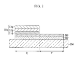
Referring to FIGS. 1-2, an organic light emitting diode (OLED) display according to a first exemplary embodiment will be described in detail. FIG. 1 is an equivalent circuit diagram of the OLED display, and FIG. 2 is a cross-sectional view of the OLED display.
As shown in FIG. 1, the OLED display includes a plurality of signal lines 121, 171, and 172, and a plurality of pixels PX connected to the plurality of signal lines and substantially arranged in a matrix format. The signal lines 121, 171, and 172 include a plurality of gate lines 121 for transmitting a gate signal (or scan signal), a plurality of data lines 171 for transmitting a data signal, and a plurality of driving voltage lines 172 for transmitting a driving voltage. The gate lines 121 are extended in a row direction and are substantially parallel with each other, and the data lines 171 and the driving voltage lines 172 are substantially arranged in a column direction and are substantially parallel with each other.
Each pixel PX includes a switching thin film transistor Qs, a driving thin film transistor Qd, a storage capacitor Cst, and an organic light emitting diode (OLED) LD. The switching thin film transistor Qs includes a control terminal, an input terminal, and an output terminal. The control terminal is connected to the gate line 121, the input terminal is connected to the data line 171, and the output terminal is connected to the driving thin film transistor Qd. The switching thin film transistor Qs transmits a data signal applied to the data line 171 to the driving thin film transistor Qd in response to a scan signal applied to the gate line 121.
The driving thin film transistor Qd includes a control terminal, an input terminal, and an output terminal. The control terminal is connected to the switching thin film transistor Qs, the input terminal is connected to the driving voltage line 172, and the output terminal is connected to the OLED LD. The driving thin film transistor Qd flows an output current ILD whose magnitude varies depending on a voltage between the control terminal and the output terminal thereof.
The storage capacitor Cst is connected between the control terminal and the input terminal of the driving thin film transistor Qd. The storage capacitor Cst charges the data signal applied to the control terminal of the driving thin film transistor Qd and maintains the charge of the data signal after the switching thin film transistor Qs is turned off.
The OLED LD includes an anode connected to the output terminal of the driving thin film transistor Qd and a cathode connected to a common voltage Vss. The OLED LD emits light that is varied in intensity depending on the output current ILD of the thin film transistor Qd to display an image.
In FIG. 1, the switching thin film transistor Qs and the driving thin film transistor Qd are depicted as n-channel field effect transistors (FETs). However, in other embodiments, at least one of the switching thin film transistor Qs or the driving thin film transistor Qd may be a p-channel field effect transistor. Further, in other embodiments, the connection relationship among the thin film transistors Qs and Qd, the storage capacitor Cst, and the OLED LD may vary.
A structure of the OLED display of FIG. 1 will now be described in further detail with reference to FIGS. 1-2.
As shown in FIG. 2, an organic emission layer 210 is disposed on a substrate 100 including a pixel area Q and a peripheral area P. The organic emission layer 210 includes the switching thin film transistor Qs, the driving thin film transistor Qd, and the OLED LD (including the anode connected to the output terminal of the driving thin film transistor Qd, and the cathode connected to the common voltage Vss).
A thin film encapsulation layer 220 is disposed on the organic emission layer 210 to encapsulate the organic emission layer 210 by covering the same. A pixel laminating film 10 q is disposed on a pixel area Q of the thin film encapsulation layer 220. Here, the pixel area Q of the thin film encapsulation layer 220 corresponds to the pixel area Q of the substrate 100. The pixel laminating film 10 q includes a plurality of pixel adhesive layers 11 q, 12 q, and 13 q, each of which may contain an acryl-based adhesive, a di-functional ultraviolet (UV) oligomer, and a hexa-functional UV oligomer. In the first exemplary embodiment shown in FIG. 2, three pixel adhesive layers 11 q, 12 q, and 13 q are exemplarily illustrated, but in other embodiments, four or more pixel adhesive layers may be provided, while in still other embodiments, two pixel adhesive layers may be provided.
The plurality of pixel adhesive layers 11 q, 12 q, and 13 q are cured such that they protect the OLED display from the external environment. The plurality of pixel adhesive layers 11 q, 12 q, and 13 q includes a lower pixel adhesive layer 11 q, a middle pixel adhesive layer 12 q, and an upper pixel adhesive layer 13 q. The lower pixel adhesive layer 11 q directly contacts the thin film encapsulation layer 220.
The upper pixel adhesive layer 13 q and the lower pixel adhesive layer 11 q are different from each other in the concentration (content) of the di-functional UV oligomer and the concentration (content) of the hexa-functional UV oligomer. That is, the upper pixel adhesive layer 13 q contains much more di-functional UV oligomer than the lower pixel adhesive layer 11 q, and the sum of the di-functional UV oligomer concentration and the hexa-functional UV oligomer concentration of the upper pixel adhesive layer 13 q is less than the sum of the di-functional UV oligomer concentration and the hexa-functional UV oligomer concentration of the lower pixel adhesive layer 11 q. The same relationship may exist with the other pixel adhesive layers (for example, the middle pixel adhesive layer 12 q) and the lower pixel adhesive layer 11 q.
In this case, the di-functional UV oligomer has a stronger adhesive force than the hexa-functional UV oligomer, and the adhesive force is increased as the sum of the di-functional UV oligomer concentration and the hexa-functional UV oligomer concentration is decreased (for example, as the concentration of hexa-functional UV oligomer is decreased). Thus, when UV light is radiated to a peripheral laminating film 10 p (refer to FIG. 5) disposed in the peripheral area P to manufacture the OLED display of FIGS. 1-2, the adhesive force of a lower peripheral adhesive layer 11 p containing much more of the hexa-functional UV oligomer than the di-functional UV oligomer (relative to those of upper peripheral adhesive layer 13 p) is weakened because the adhesive force of the hexa-functional UV oligomer becomes weaker (e.g., significantly weaker) after the UV light irradiation compared to that of the di-functional UV oligomer. Accordingly, the lower peripheral adhesive layer 11 p disposed in the peripheral area P can be easily peeled from the thin film encapsulation layer 220.
The manufacturing method of the OLED display according to the first exemplary embodiment will now be described in further detail with reference to FIGS. 3-6. FIG. 3 is a cross-sectional view of a laminating film of the OLED display of FIGS. 1-2, and FIGS. 4-6 are cross-sectional views illustrating a manufacturing method of the OLED display of FIGS. 1-3.
First, as shown in FIG. 3, a laminating film 30 that includes an adhesive layer 10, an upper protective layer 22, and a lower protective layer 21 is provided. The adhesive layer 10 includes a lower adhesive layer 11, a middle adhesive layer 12, and an upper adhesive layer 13. The upper protective layer 22 covers the upper adhesive layer 13, and the lower protective layer 21 covers the lower adhesive layer 11. The adhesive layer 10 (for example, each of the lower adhesive layer 11, middle adhesive layer 12, and upper adhesive layer 13) contains an acryl-based adhesive, a di-functional UV oligomer, and a hexa-functional UV oligomer.
Next, as shown in FIG. 4, the organic emission layer 210 and the thin film encapsulation layer 220 covering the organic emission layer 210 are disposed on the substrate 100 that includes the pixel area Q and the peripheral area P (see FIG. 6). In addition, the lower protective layer 21 is peeled from the laminating film 30 (see FIG. 3) to expose the lower adhesive layer 11. Then, the lower adhesive layer 11 of the laminating film 30 is adhered to the thin film encapsulation layer 220.
Next, as shown in FIG. 5, UV light is radiated to a peripheral laminating film 10 p that corresponds to the peripheral area P of the substrate 100 to change the adhesive force of peripheral adhesive layers 11 p, 12 p, and 13 p. The peripheral adhesive layers include lower peripheral adhesive layer 11 p, middle peripheral adhesive layer 12 p, and upper peripheral adhesive layer 13 p.
FIG. 7 is a graph illustrating the change of the adhesive force according to the concentration of the di-functional UV oligomer before and after UV light irradiation. FIG. 8 is a graph illustrating the change of the adhesive force according to the concentration of hexa-functional UV oligomer before and after UV light irradiation.
As shown in FIGS. 7-8, the adhesive force of the di-functional UV oligomer is increased relative to that of the hexa-functional UV oligomer after UV light irradiation. Accordingly, the adhesive force of an adhesive layer is decreased after UV light irradiation as the concentration of the di-functional UV oligomer is decreased relative to the concentration of the hexa-functional UV oligomer.
Thus, since the UV-irradiated lower peripheral adhesive layer 11 p contains less of the di-functional UV oligomer than the UV-irradiated upper peripheral adhesive layer 13 p, the adhesive force of the lower peripheral adhesive layer 11 p becomes weaker than that of the upper peripheral adhesive layer 13 p. Accordingly, adhesion between the lower peripheral adhesive layer 11 p of the laminating film 30 and the thin film encapsulation layer 220 is decreased.
Further, when the sum of the di-functional UV oligomer concentration and the hexa-functional UV oligomer concentration of the upper peripheral adhesive layer 13 p is less than that of the lower peripheral adhesive layer 11 p, it follows that the lower peripheral adhesive layer 11 p has a significantly higher concentration of the hexa-functional UV oligomer than the upper peripheral adhesive layer 13 p. Accordingly, the adhesion between the lower peripheral adhesive layer 11 p of the laminating film 30 and the thin film encapsulation layer 220 is further decreased after UV light irradiation.
Next, as shown in FIG. 6, the peripheral laminating film 10 p is peeled from the thin film encapsulation layer 220 and the pixel laminating film 10 q remains. In this case, since the adhesion between the lower peripheral adhesive layer 11 p of the peripheral laminating film 10 p and the thin film encapsulation layer 220 is decreased, the lower peripheral adhesive layer 11 p of the peripheral laminating film 10 p can be easily peeled from the thin film encapsulation layer 220.
Further, the adhesive force of the upper peripheral adhesive layer 13 p is stronger than that of the lower peripheral adhesive layer 11 p, and therefore the upper peripheral adhesive layer 13 p and the upper protective layer 22 remain adhered to each other. In addition, the upper protective layer 22 at a location corresponding to the pixel area Q of the substrate 100 is peeled from the upper pixel adhesive layer 13 q while the peripheral laminating film 10 p is peeled from the thin film encapsulation layer 220 at the same time.
Finally, the pixel laminating film 10 q corresponding to the pixel area Q of the substrate 100 is cured.
As described, the di-functional UV oligomer concentration of the upper adhesive layer 13 of the laminating film 30 is larger than that of the lower adhesive layer 11, the sum of the di-functional UV oligomer concentration and the hexa-functional UV oligomer concentration of the upper adhesive layer 13 is less than that of the lower adhesive layer 11, and the adhesive force of the lower peripheral adhesive layer 11 p disposed in the peripheral area P is weakened by the UV irradiation. Consequently, the pixel laminating film 10 q can be patterned by easily peeling the lower peripheral adhesive layer 11 p from the thin film encapsulation layer 220.
Accordingly, when the OLED display model is changed, the pattern of the pixel laminating film 10 q can be easily changed using the peeling process of the peripheral laminating film 10 p. Further, the process time and the process cost can be reduced because an additional cutting device or press device is not required.
It should be noted that in the first exemplary embodiment (illustrated in FIGS. 1-6), only the laminating film is patterned. In other embodiments, the laminating film 30 and the thin film encapsulation layer 220 may be simultaneously patterned. Hereinafter, an OLED display according to a second exemplary embodiment will be described in further detail with reference to FIG. 9.
FIG. 9 is a cross-sectional view of the OLED display according to the second exemplary embodiment.
The second exemplary embodiment is substantially the same as the first exemplary embodiment shown in FIG. 2 except that a thin film encapsulation layer is patterned, such that repeated description will not be provided.
As shown in FIG. 9, an organic emission layer 210 is disposed on a substrate 100 including a pixel area Q and a peripheral area P. A pixel thin film encapsulation layer 220 q encapsulates the organic emission layer 210 by covering the same. The pixel thin film encapsulation layer 220 q is disposed in the pixel area Q, and contains a di-functional UV oligomer and a hexa-functional UV oligomer.
A pixel laminating film 10 q is disposed on the pixel thin film encapsulation layer 220 q. The pixel laminating film 10 q includes a plurality of pixel adhesive layers 11 q, 12 q, and 13 q, each of which may contain an acryl-based adhesive, a di-functional UV oligomer, and a hexa-functional UV oligomer. The plurality of pixel adhesive layers 11 q, 12 q, and 13 q are cured such that they protect the OLED display from the external environment. The number of pixel adhesive layers in the pixel laminating film 10 q is not limited to three. In other embodiments, one or more pixel adhesive layers may be used.
The plurality of pixel adhesive layers 11 q, 12 q, and 13 q include a lower pixel adhesive layer 11 q, a middle pixel adhesive layer 12 q, and an upper pixel adhesive layer 13 q. The upper pixel adhesive layer 13 q and the pixel thin film encapsulation layer 220 q are different from each other in the concentration of the di-functional UV oligomer and the concentration of the hexa-functional UV oligomer. That is, the di-functional UV oligomer concentration of the upper pixel adhesive layer 13 q is larger than that of the pixel thin film encapsulation layer 220 q, and the sum of the di-functional UV oligomer concentration and the hexa-functional UV oligomer concentration of the upper pixel adhesive layer 13 q is less than that of the pixel thin film encapsulation layer 220 q. The same relationship may exist with the other pixel adhesive layers (for example, the lower pixel adhesive layer 11 q and the middle pixel adhesive layer 12 q) and the pixel thin film encapsulation layer 220 q.
Here, the di-functional UV oligomer has a stronger adhesive force than the hexa-functional UV oligomer. Further, the adhesive force is increased as the sum of the di-functional UV oligomer concentration and the hexa-functional UV oligomer concentration is decreased.
Thus, when UV light is radiated to a peripheral laminating film 10 p (refer to FIG. 10) and a peripheral thin film encapsulation layer 220 p (refer to FIG. 10) disposed in the peripheral area P to manufacture the OLED display of FIG. 9, the adhesive force of the peripheral thin film encapsulation layer 220 p that contains much more of the hexa-functional UV oligomer than the di-functional UV oligomer (relative to those of the upper peripheral adhesive layer 13 p) is weakened because the adhesive force of the hexa-functional UV oligomer is weakened more than that of the di-functional UV oligomer after the UV light irradiation. Accordingly, the peripheral thin film encapsulation layer 220 p disposed in the peripheral area P can be easily peeled from the organic emission layer 210.
A manufacturing method of the OLED display according to the second exemplary embodiment will now be described in further detail with reference to FIGS. 10-11.
FIGS. 10-11 are cross-sectional views of the manufacturing method of the OLED display of FIG. 9.
First, as shown in FIG. 10, the organic emission layer 210 and the thin film encapsulation layers 220 p and 220 q covering the organic emission layer 210 are disposed on the substrate 100 including the pixel area Q and the peripheral area P. Referring back to FIG. 3, a lower protective layer 21 is peeled off a laminating film 30 and a lower adhesive layer 11 is exposed. Then, the lower adhesive layer 11 of the laminating film 30 is adhered to the thin film encapsulation layers 220 p and 220 q. In this case, the thin film encapsulation layers 220 p and 220 q each contain a di-functional UV oligomer and a hexa-functional UV oligomer.
In addition, the adhesive force of the peripheral adhesive layers 11 p, 12 p, and 13 p, and the adhesive force of the peripheral thin film encapsulation layer 220 p are changed by radiating UV light on the peripheral laminating film 10 p and the peripheral thin film encapsulation layer 220 p that correspond to the peripheral area P of the substrate 100.
Since the UV-irradiated peripheral thin film encapsulation layer 220 p contains less of the di-functional UV oligomer than the UV-irradiated upper peripheral adhesive layer 13 p, the adhesive force of the peripheral thin film encapsulation layer 220 p becomes weaker than that of the upper peripheral adhesive layer 13 p. Accordingly, adhesion between the peripheral thin film encapsulation layer 220 p and the organic emission layer 210 is decreased. In addition, since the sum of the di-functional UV oligomer concentration and the hexa-functional UV oligomer concentration of the upper peripheral adhesive layer 13 p is less than that of the peripheral thin film encapsulation layer 220 p, the adhesion between the peripheral thin film encapsulation layer 220 p and the organic emission layer 210 is further decreased.
Next, as shown in FIG. 11, the peripheral laminating film 10 p and the peripheral thin film encapsulation layer 220 p are peeled from the organic emission layer 210 and the pixel laminating film 10 q and the pixel thin film encapsulation layer 220 q remain. In this case, since the adhesion between the peripheral thin film encapsulation layer 220 p and the organic emission layer 210 is decreased, the peripheral thin film encapsulation layer 220 p can be easily peeled from the organic emission layer 210.
Further, the adhesive force of the upper peripheral adhesive layer 13 p is stronger than that of the peripheral thin film encapsulation layer 220 p. Accordingly, the upper peripheral adhesive layer 13 p and the upper protective layer 22 remain adhered to each other. In addition, the upper protective layer 22 at a location corresponding to the pixel area Q of the substrate 100 is peeled from the upper pixel adhesive layer 13 q concurrently with the peeling of the peripheral laminating film 10 p and the peripheral thin film encapsulation layer 220 p from the organic emission layer 210.
Finally, the pixel laminating film 10 q that corresponds to the pixel area Q of the substrate 100 is cured.
As described, (1) the di-functional UV oligomer concentration of the upper adhesive layer 13 of the laminating film 30 is larger than that of the thin film encapsulation layers 220 p and 220 q, (2) the sum of the di-functional UV oligomer concentration and the hexa-functional UV oligomer concentration of the upper adhesive layer 13 is less than that of the thin film encapsulation layers 220 p and 220 q, and (3) the adhesive force of the peripheral thin film encapsulation layer 220 disposed in the peripheral area P is weakened by the UV light irradiation. Accordingly, the pixel laminating film 10 q and the pixel thin film encapsulation layer 220 q can be concurrently (for example, simultaneously or concurrently) patterned by easily peeling the peripheral thin film encapsulation layer 220 p from the organic emission layer 210.
Accordingly, as described, process time and manufacturing cost can be reduced by simultaneously patterning the laminating film 30 and the thin film encapsulation layers 220 p and 220 q. Further, an additional cutting device or press device is not required for patterning of the laminating film 30 and the thin film encapsulation layers 220 p and 220 q, so that the process time can be shortened and the process cost can be reduced.
While the present invention has been described in connection with what is presently considered to be practical exemplary embodiments, it is to be understood that the invention is not limited to the disclosed embodiments, but, on the contrary, is intended to cover various modifications and equivalent arrangements included within the spirit and scope of the appended claims, and equivalents thereof.
Description of Selected Symbols
10p: peripheral laminating film 10q: pixel laminating film
11p: lower peripheral adhesive layer 11q: lower pixel adhesive layer
13p: upper peripheral adhesive layer 13q: upper pixel adhesive layer
210: organic emission layer 220: thin film encapsulation layer
220p: peripheral thin film 220q: pixel thin film encapsulation
encapsulation layer layer

Claims (19)

What is claimed is:
1. An organic light emitting diode (OLED) display comprising:
an organic emission layer on a substrate including a pixel area and a peripheral area;
a thin film encapsulation layer covering the organic emission layer corresponding to the pixel area of the substrate; and
a pixel laminating film covering the thin film encapsulation layer corresponding to the pixel area of the substrate, and including one or more pixel adhesive layers that each comprise an acryl-based adhesive, a di-functional ultraviolet (UV) oligomer, and a hexa-functional UV oligomer, wherein an upper pixel adhesive layer and a lower pixel adhesive layer from among the pixel adhesive layers have different di-functional UV oligomer concentrations and different hexa-functional UV oligomer concentrations.
2. The OLED display of claim 1, wherein a di-functional UV oligomer concentration of the upper pixel adhesive layer is larger than a di-functional UV oligomer concentration of the lower pixel adhesive layer.
3. The OLED display of claim 1, wherein a sum of the di-functional UV oligomer concentration and a hexa-functional UV oligomer concentration of the upper pixel adhesive layer is less than a sum of the di-functional UV oligomer concentration and a hexa-functional UV oligomer concentration of the lower pixel adhesive layer.
4. The OLED display of claim 1, wherein the thin film encapsulation layer corresponds to the pixel area of the substrate, and
comprises the di-functional UV oligomer and the hexa-functional UV oligomer.
5. The OLED display of claim 4, wherein an upper pixel adhesive layer from among the pixel adhesive layers and the thin film encapsulation layer have different di-functional UV oligomer concentrations and different hexa-functional UV oligomer concentrations.
6. The OLED display of claim 5, wherein a di-functional UV oligomer concentration of the thin film encapsulation layer is less than a di-functional UV oligomer concentration of the upper pixel adhesive layer.
7. The OLED display of claim 5, wherein a sum of the di-functional UV oligomer concentration and a hexa-functional UV oligomer concentration of the thin film encapsulation layer is larger than a sum of the di-functional UV oligomer concentration and a hexa-functional UV oligomer concentration of the upper pixel adhesive layer.
8. A manufacturing method of an organic light emitting diode (OLED) display, comprising:
forming an organic emission layer and a thin film encapsulation layer covering the organic emission layer on a substrate including a pixel area and a peripheral area;
adhering a laminating film comprising a plurality of adhesive layers and an upper protective layer that covers an upper adhesive layer from among the plurality of adhesive layers on the thin film encapsulation layer, a lower adhesive layer from among the plurality of adhesive layers contacting the thin film encapsulation layer;
radiating ultraviolet (UV) light on the laminating film that corresponds to the peripheral area of the substrate to decrease adhesion between the lower adhesive layer and the thin film encapsulation layer corresponding to the peripheral area of the substrate; and
peeling the laminating film corresponding to the peripheral area of the substrate from the thin film encapsulation layer to maintain the laminating film that corresponds to the pixel area of the substrate.
9. The manufacturing method of claim 8, wherein each of the plurality of adhesive layers contains an acryl-based adhesive, a di-functional UV oligomer, and a hexa-functional UV oligomer.
10. The manufacturing method of claim 9, wherein a di-functional UV oligomer concentration of the upper adhesive layer is larger than a di-functional UV oligomer concentration of the lower adhesive layer.
11. The manufacturing method of claim 10, wherein a sum of the di-functional UV oligomer concentration and a hexa-functional UV oligomer concentration of the upper adhesive layer is less than a sum of the di-functional UV oligomer concentration and a hexa-functional UV oligomer concentration of the lower adhesive layer.
12. The manufacturing method of claim 8, wherein the peeling of the laminating film corresponding to the peripheral area of the substrate comprises peeling the upper protective layer that corresponds to the pixel area of the substrate from the upper adhesive layer.
13. The manufacturing method of claim 8, further comprising curing the laminating film that corresponds to the pixel area of the substrate after the peeling of the laminating film corresponding to the peripheral area of the substrate.
14. A manufacturing method of an organic light emitting diode (OLED) display, comprising:
forming an organic emission layer and a thin film encapsulation layer that covers the organic emission layer and contains a di-functional ultraviolet (UV) oligomer and a hexa-functional UV oligomer on a substrate including a pixel area and a peripheral area;
adhering a laminating film comprising one or more adhesive layers and an upper protective layer covering an upper adhesive layer from among the adhesive layers on the thin film encapsulation layer;
radiating ultraviolet (UV) light on the laminating film and the thin film encapsulation layer that corresponds to the peripheral area of the substrate to decrease adhesion between the thin film encapsulation layer and the organic emission layer corresponding to the peripheral area of the substrate; and
peeling the laminating film and the thin film encapsulation layer corresponding to the peripheral area of the substrate from the organic emission layer to maintain the laminating film and the thin film encapsulation layer corresponding to the pixel area of the substrate.
15. The manufacturing method of claim 14, wherein each of the adhesive layers contain an acryl-based adhesive, a di-functional UV oligomer, and a hexa-functional UV oligomer.
16. The manufacturing method of claim 15, wherein a di-functional UV oligomer concentration of the thin film encapsulation layer is less than a di-functional UV oligomer concentration of the upper adhesive layer.
17. The manufacturing method of claim 16, wherein a sum of the di-functional UV oligomer concentration and a hexa-functional UV oligomer concentration of the thin film encapsulation layer is larger than a sum of the di-functional UV oligomer concentration and a hexa-functional UV oligomer concentration of the upper adhesive layer.
18. The manufacturing method of claim 14, wherein the peeling of the laminating film and the thin film encapsulation layer corresponding to the peripheral area of the substrate comprises peeling the upper protective layer that corresponds to the pixel area of the substrate from the upper adhesive layer.
19. The manufacturing method of claim 14, further comprising curing the laminating film that corresponds to the pixel area of the substrate after the peeling of the laminating film and the thin film encapsulation layer corresponding to the peripheral area of the substrate.
US13/302,321 2011-04-11 2011-11-22 Organic light emitting diode display and manufacturing method thereof Active 2032-11-05 US8729797B2 (en)

Applications Claiming Priority (2)

Application Number Priority Date Filing Date Title
KR1020110033397A KR20120115842A (en) 2011-04-11 2011-04-11 Organic light emitting diode display and manufacturing method thereof
KR10-2011-0033397 2011-04-11

Publications (2)

Publication Number Publication Date
US20120256534A1 US20120256534A1 (en) 2012-10-11
US8729797B2 true US8729797B2 (en) 2014-05-20

Family

ID=46965557

Family Applications (1)

Application Number Title Priority Date Filing Date
US13/302,321 Active 2032-11-05 US8729797B2 (en) 2011-04-11 2011-11-22 Organic light emitting diode display and manufacturing method thereof

Country Status (2)

Country Link
US (1) US8729797B2 (en)
KR (1) KR20120115842A (en)

Cited By (3)

* Cited by examiner, † Cited by third party
Publication number Priority date Publication date Assignee Title
US20130285064A1 (en) * 2012-04-27 2013-10-31 Kabushiki Kaisha Toshiba Semiconductor light emitting device
US9812667B2 (en) 2015-11-04 2017-11-07 Microsoft Technology Licensing, Llc Patterning of OLED display stacks
US11732077B2 (en) 2020-11-09 2023-08-22 Samsung Display Co., Ltd. Resin composition, adhesive member, and display device

Families Citing this family (7)

* Cited by examiner, † Cited by third party
Publication number Priority date Publication date Assignee Title
KR102092706B1 (en) 2013-09-02 2020-04-16 삼성디스플레이 주식회사 Composition, organic light-emitting display apparatus comprising the composition and the manufacturing method of the organic light-emitting display apparatus
KR102104334B1 (en) * 2013-09-04 2020-04-27 삼성디스플레이 주식회사 Method for manufacturing organic light emitting diode display
US9626145B1 (en) 2014-06-27 2017-04-18 X Development Llc Tileable display with pixel-tape
US10354577B1 (en) 2015-06-02 2019-07-16 X Development Llc Masking non-functioning pixels in a display
US10310314B2 (en) 2015-08-14 2019-06-04 X Development Llc Bright edge display for seamless tileable display panels
DE102016108195A1 (en) * 2016-05-03 2017-11-09 Osram Oled Gmbh METHOD FOR PRODUCING AN ORGANIC OPTOELECTRONIC COMPONENT AND ORGANIC OPTOELECTRONIC COMPONENT
CN111063824B (en) * 2019-12-09 2022-12-27 昆山国显光电有限公司 Display panel and display device

Citations (5)

* Cited by examiner, † Cited by third party
Publication number Priority date Publication date Assignee Title
KR20060020051A (en) 2004-08-30 2006-03-06 삼성에스디아이 주식회사 Method for forming organic layer and method for fabricating oled
KR20070060689A (en) 2005-12-09 2007-06-13 (주)에스티아이 Apparatus and method for laminating film with means for patterning film
KR20100019650A (en) 2008-08-11 2010-02-19 주식회사 세코닉스 Method of manufacturing an multifunction optical filter as plasma display panel using roll stamper
KR20100110173A (en) * 2009-04-02 2010-10-12 (주)유비스재료기술 Uv curing composition and keypad using the same and the manufacturing method thereof
US20120043126A1 (en) * 2010-08-20 2012-02-23 Samsung Electro-Mechanics Co., Ltd. Printed circuit board and method of manufacturing the same

Patent Citations (5)

* Cited by examiner, † Cited by third party
Publication number Priority date Publication date Assignee Title
KR20060020051A (en) 2004-08-30 2006-03-06 삼성에스디아이 주식회사 Method for forming organic layer and method for fabricating oled
KR20070060689A (en) 2005-12-09 2007-06-13 (주)에스티아이 Apparatus and method for laminating film with means for patterning film
KR20100019650A (en) 2008-08-11 2010-02-19 주식회사 세코닉스 Method of manufacturing an multifunction optical filter as plasma display panel using roll stamper
KR20100110173A (en) * 2009-04-02 2010-10-12 (주)유비스재료기술 Uv curing composition and keypad using the same and the manufacturing method thereof
US20120043126A1 (en) * 2010-08-20 2012-02-23 Samsung Electro-Mechanics Co., Ltd. Printed circuit board and method of manufacturing the same

Non-Patent Citations (1)

* Cited by examiner, † Cited by third party
Title
Kim, In Beom, et al., "Adhesive and Removable Characteristics of UV Curable Adhesive", Korean Chem. Eng. Res., vol. 46, No. 1, Feb. 2008, pp. 76-81.

Cited By (4)

* Cited by examiner, † Cited by third party
Publication number Priority date Publication date Assignee Title
US20130285064A1 (en) * 2012-04-27 2013-10-31 Kabushiki Kaisha Toshiba Semiconductor light emitting device
US8994030B2 (en) * 2012-04-27 2015-03-31 Kabushiki Kaisha Toshiba Semiconductor light emitting device
US9812667B2 (en) 2015-11-04 2017-11-07 Microsoft Technology Licensing, Llc Patterning of OLED display stacks
US11732077B2 (en) 2020-11-09 2023-08-22 Samsung Display Co., Ltd. Resin composition, adhesive member, and display device

Also Published As

Publication number Publication date
US20120256534A1 (en) 2012-10-11
KR20120115842A (en) 2012-10-19

Similar Documents

Publication Publication Date Title
US8729797B2 (en) Organic light emitting diode display and manufacturing method thereof
US20200119116A1 (en) Flexible organic electroluminescent device and method for fabricating the same
US9000428B2 (en) Organic light emitting diode display
US7595854B2 (en) Organic light emitting display device
KR20200036839A (en) Organic light emitting device and manufacturing method thereof
US20170069271A1 (en) Display apparatus
US20090026932A1 (en) Organic light emitting display and method of manufacturing the same
US9455304B2 (en) Organic light-emitting diode display with white and blue diodes
US6965361B1 (en) Method of manufacture of active matrix addressed polymer LED display
KR101080353B1 (en) Thin film transistor array panel
KR101808300B1 (en) Organic light emitting diode display
CN106066729B (en) Organic light emitting diode display and method of manufacturing the same
US20170047391A1 (en) Organic light emitting diode display and manufacturing method thereof
CN111564481B (en) Display substrate, manufacturing method thereof and display device
CN109285964B (en) Flexible display panel, preparation method thereof and flexible display device
US8841761B2 (en) Organic light emitting diode display
US9178002B2 (en) Organic light-emitting diode (OLED) display
KR102280777B1 (en) Display device and manufacturing method thereof
US11348991B2 (en) Display device having opening in protective substrate at bending area and method of fabricating the same
US11374067B2 (en) Display device
US8987773B2 (en) Organic light emitting diode display
US20130020967A1 (en) Organic light emitting diode display
CN114497124A (en) Display device
CN106098729B (en) Organic light emitting diode display
US9276044B2 (en) Display device and method for manufacturing display device

Legal Events

Date Code Title Description
AS Assignment

Owner name: SAMSUNG MOBILE DISPLAY CO., LTD., KOREA, REPUBLIC

Free format text: ASSIGNMENT OF ASSIGNORS INTEREST;ASSIGNORS:LEE, SO-YOUNG;CHO, YOON-HYEUNG;OH, MIN-HO;AND OTHERS;REEL/FRAME:027277/0150

Effective date: 20111114

AS Assignment

Owner name: SAMSUNG DISPLAY CO., LTD., KOREA, REPUBLIC OF

Free format text: MERGER;ASSIGNOR:SAMSUNG MOBILE DISPLAY CO., LTD.;REEL/FRAME:028840/0224

Effective date: 20120702

FEPP Fee payment procedure

Free format text: PAYOR NUMBER ASSIGNED (ORIGINAL EVENT CODE: ASPN); ENTITY STATUS OF PATENT OWNER: LARGE ENTITY

STCF Information on status: patent grant

Free format text: PATENTED CASE

MAFP Maintenance fee payment

Free format text: PAYMENT OF MAINTENANCE FEE, 4TH YEAR, LARGE ENTITY (ORIGINAL EVENT CODE: M1551)

Year of fee payment: 4

MAFP Maintenance fee payment

Free format text: PAYMENT OF MAINTENANCE FEE, 8TH YEAR, LARGE ENTITY (ORIGINAL EVENT CODE: M1552); ENTITY STATUS OF PATENT OWNER: LARGE ENTITY

Year of fee payment: 8