US8670243B2 - Semiconductor memory device - Google Patents
Semiconductor memory device Download PDFInfo
- Publication number
- US8670243B2 US8670243B2 US13/046,896 US201113046896A US8670243B2 US 8670243 B2 US8670243 B2 US 8670243B2 US 201113046896 A US201113046896 A US 201113046896A US 8670243 B2 US8670243 B2 US 8670243B2
- Authority
- US
- United States
- Prior art keywords
- semiconductor memory
- controller
- memory device
- housing
- substrate
- Prior art date
- Legal status (The legal status is an assumption and is not a legal conclusion. Google has not performed a legal analysis and makes no representation as to the accuracy of the status listed.)
- Active, expires
Links
Images


Classifications
-
- H—ELECTRICITY
- H05—ELECTRIC TECHNIQUES NOT OTHERWISE PROVIDED FOR
- H05K—PRINTED CIRCUITS; CASINGS OR CONSTRUCTIONAL DETAILS OF ELECTRIC APPARATUS; MANUFACTURE OF ASSEMBLAGES OF ELECTRICAL COMPONENTS
- H05K7/00—Constructional details common to different types of electric apparatus
- H05K7/02—Arrangements of circuit components or wiring on supporting structure
- H05K7/06—Arrangements of circuit components or wiring on supporting structure on insulating boards, e.g. wiring harnesses
-
- H—ELECTRICITY
- H05—ELECTRIC TECHNIQUES NOT OTHERWISE PROVIDED FOR
- H05K—PRINTED CIRCUITS; CASINGS OR CONSTRUCTIONAL DETAILS OF ELECTRIC APPARATUS; MANUFACTURE OF ASSEMBLAGES OF ELECTRICAL COMPONENTS
- H05K1/00—Printed circuits
- H05K1/02—Details
- H05K1/11—Printed elements for providing electric connections to or between printed circuits
- H05K1/117—Pads along the edge of rigid circuit boards, e.g. for pluggable connectors
-
- H—ELECTRICITY
- H05—ELECTRIC TECHNIQUES NOT OTHERWISE PROVIDED FOR
- H05K—PRINTED CIRCUITS; CASINGS OR CONSTRUCTIONAL DETAILS OF ELECTRIC APPARATUS; MANUFACTURE OF ASSEMBLAGES OF ELECTRICAL COMPONENTS
- H05K7/00—Constructional details common to different types of electric apparatus
- H05K7/20—Modifications to facilitate cooling, ventilating, or heating
- H05K7/2039—Modifications to facilitate cooling, ventilating, or heating characterised by the heat transfer by conduction from the heat generating element to a dissipating body
-
- H—ELECTRICITY
- H05—ELECTRIC TECHNIQUES NOT OTHERWISE PROVIDED FOR
- H05K—PRINTED CIRCUITS; CASINGS OR CONSTRUCTIONAL DETAILS OF ELECTRIC APPARATUS; MANUFACTURE OF ASSEMBLAGES OF ELECTRICAL COMPONENTS
- H05K1/00—Printed circuits
- H05K1/18—Printed circuits structurally associated with non-printed electric components
- H05K1/181—Printed circuits structurally associated with non-printed electric components associated with surface mounted components
-
- H—ELECTRICITY
- H05—ELECTRIC TECHNIQUES NOT OTHERWISE PROVIDED FOR
- H05K—PRINTED CIRCUITS; CASINGS OR CONSTRUCTIONAL DETAILS OF ELECTRIC APPARATUS; MANUFACTURE OF ASSEMBLAGES OF ELECTRICAL COMPONENTS
- H05K2201/00—Indexing scheme relating to printed circuits covered by H05K1/00
- H05K2201/10—Details of components or other objects attached to or integrated in a printed circuit board
- H05K2201/10007—Types of components
- H05K2201/10159—Memory
-
- H—ELECTRICITY
- H05—ELECTRIC TECHNIQUES NOT OTHERWISE PROVIDED FOR
- H05K—PRINTED CIRCUITS; CASINGS OR CONSTRUCTIONAL DETAILS OF ELECTRIC APPARATUS; MANUFACTURE OF ASSEMBLAGES OF ELECTRICAL COMPONENTS
- H05K2201/00—Indexing scheme relating to printed circuits covered by H05K1/00
- H05K2201/10—Details of components or other objects attached to or integrated in a printed circuit board
- H05K2201/10007—Types of components
- H05K2201/10189—Non-printed connector
Definitions
- Embodiments described herein relate generally to a semiconductor memory device.
- USB Universal Serial Bus
- USB1.1 to USB3.0 are of backward compatibility and required to correctly operate when connecting a lower standard product and an upper standard product to each other except that its function and performance are restricted by the lower standard.
- USB memory As one of the peripheral devices to be connected to the information processing device via the USB socket, a memory device in which a nonvolatile flash memory and a controller are mounted to a printed substrate together with a USB connector (Standard-A) and housed in a casing, which is a so-called USB memory, has been known (see Japanese Patent Application Laid-Open No. 2007-156682).
- USB memory products complying with USB2.0 having a maximum transfer speed of 480 Mbits/s are currently predominant.
- USB memory capacity of a USB memory has been steadily increasing. Also, there is a tendency that an amount of data per file handled by an information processing device is increased. Therefore, in order to realize higher speed data transfer between the information processing device and the USB memory, there is a demand for development of a USB memory complying with USB3.0 having a maximum transfer speed of 5 Gbits/s.
- USB memory complying with USB3.0 is required to transfer data at a speed prescribed in the standard in both of the cases of data transfers at USB 3.0 or USB 2.0.
- any specific configuration for realizing the data transfer has not been proposed.
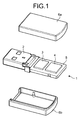
- FIG. 1 is an exploded perspective view showing a USB memory according to a first embodiment
- FIG. 2 is a diagram showing arrangement of terminals of a USB connector complying with USB3.0;
- FIGS. 3A to 3D are diagrams showing a configuration of the USB memory according to the first embodiment in a state where an upper casing and a lower casing are not mounted;
- FIG. 4 is a diagram showing one example of connection between terminals of a USB connector and pins of a controller in a USB memory complying with USB2.0;
- FIG. 5 is a diagram showing one example of connection between terminals of a USB connector and pins of a controller in a substrate of the USB memory according to the first embodiment
- FIG. 6A and FIG. 6B are diagrams showing a configuration of a USB memory according to a second embodiment in a state where an upper casing and a lower casing are not mounted;
- FIG. 7 is a diagram showing one example of connection between terminals of a USB connector and pins of a controller in a substrate of the USB memory according to the second embodiment
- FIG. 8A to FIG. 8D are diagrams showing a configuration of a USB memory according to a third embodiment in a state where an upper casing and a lower casing are not mounted;
- FIG. 9 is a diagram showing one example of connection in the case where any pin for data transfer at USB2.0 is not allocated at a peripheral part of the controller and a side where the USB connector are mounted;
- FIG. 10A and FIG. 10B are diagrams showing a configuration of a USB memory according to a fourth embodiment in a state where an upper casing and a lower casing are not mounted;
- FIG. 11A to FIG. 11C are diagrams showing a configuration of a USB memory according to a fifth embodiment
- FIG. 12A to FIG. 12F are diagrams showing a configuration of a USB memory according to a sixth embodiment
- FIG. 13A to FIG. 13C are diagrams showing a configuration of a USB memory according to a seventh embodiment
- FIG. 14A to FIG. 14C are diagrams showing a configuration of a USB memory according to an eighth embodiment
- FIG. 15A to FIG. 15C are diagrams showing a configuration of a USB memory according to a ninth embodiment
- FIG. 16A to FIG. 16C are diagrams showing a configuration of a USB memory according to a tenth embodiment.
- FIG. 17A and FIG. 17B are diagrams showing temperature simulation results of the USB memories according to fifth to tenth embodiments.
- semiconductor memory device is capable of operating at a first mode and a second mode which is higher in speed than the first mode.
- the semiconductor memory device comprising: a semiconductor memory; a controller which controls the semiconductor memory; a connector which is provided with terminals for sending and receiving data to and from an external device; and a substrate on which the semiconductor memory, the controller, and the connector are mounted, the substrate comprising a plurality of wiring layers.
- the controller and the connector are mounted on an identical surface of the substrate.
- the substrate comprises a wiring which connects a mounting pad for the terminal for data transfer at the second mode of the connector and a mounting pad for a pin for data transfer at the second mode of the controller to each other on the wiring layer on a mounting surface for the connector and the controller.
- FIG. 1 is an exploded perspective view showing a USB memory according to a first embodiment.
- a USB memory 1 according to the present embodiment complies with USB3.0 and compatible with USB2.0 due to backward compatibility.
- the USB memory 1 has a configuration in which a substrate 5 on which a USB connector 2 , a controller 3 , a memory package 4 , and the like are mounted is housed in a housing including an upper casing 6 a and a lower casing 6 b .
- the memory package 4 is a nonvolatile semiconductor memory such as a NAND flash memory.
- the controller 3 controls the memory package 4 to perform data reading and data writing.
- the USB connector 2 is an interface for connection with a host device provided with a USB socket and provided with both of a terminal for data transfer at USB3.0 and a terminal for data transfer at USB2.0.
- FIG. 2 is a diagram showing arrangement of terminals of the USB connector 2 complying with USB3.0.
- the USB connector 2 is provided with a GND terminal 81 , D+ terminal 82 , a D ⁇ terminal 83 , and a VBUS terminal 84 as terminals for data transfer at USB 2.0 at a leading end side in a direction of insertion into USB socket.
- the USB connector 2 is provided with a SSRX+ terminal 91 , a SSRX ⁇ terminal 92 , a GND terminal 93 , a SSTX ⁇ terminal 94 , and a SSTX+ terminal 95 as terminals for data transfer at USB 3.0 at a tail end side in the direction of insertion into USB socket.
- FIGS. 3A to 3D are diagrams showing a configuration of the USB memory 1 in a state where the upper casing 6 a and the lower casing 6 b are not mounted.
- FIG. 3A is a top view
- FIG. 3B is a side sectional view taken along a line IIIB-IIIB of FIG. 3A
- FIG. 3C is a side view
- FIG. 3D is a bottom view.
- the controller 3 is a QFP (Quad Flat Package) and mounted to the substrate 5 via pins projected from four sides.
- the substrate 5 is a multilayer substrate provided with wiring layers including two layers provided respectively on top and bottom surfaces thereof and two layers inside.
- the layers are referred to as a first wiring layer, a second wiring layer, a third wiring layer, and a fourth wiring layer from the top surface side as required to distinguish the wiring layers from one another.
- the USB connector 2 and the controller 3 are mounted on the first wiring layer on the top surface of the substrate 5 .
- the memory package 4 is provided on each of the top surface and the bottom surface (i.e. the first wiring layer and the fourth wiring layer).
- the memory package 4 may be mounted only on one of the surfaces of the substrate 5 , or two or more memory packages may be provided on at least one of the surfaces of the substrate 5 .
- the memory package 4 has a plurality of internal memory chips.
- the controller 3 is capable of partially using the memory package 4 by dividing the memory package 4 by the unit of chip by controlling a ready/busy pin or a chip enable pin of the memory package 4 .
- the controller 3 is capable of simultaneously operating the plurality of chips inside the memory package 4 by the unit of chip or operating a plurality of packages by the unit of package by using an interleave function and a parallel mode function.
- the controller 3 is capable of sending and receiving data at a high speed to and from the memory package 4 by simultaneously driving the plurality of memory packages 4 and the plurality of memory chips inside the memory packages 4 .
- USB memory 1 Since the USB memory 1 according to the present embodiment is compatible with USB2.0 by the backward compatibility, a wiring between terminals of a USB connector of USB2.0 standard and pins of a controller will be described first as a reference example gathered by the inventor.
- FIG. 4 is a diagram showing one example of connection between terminals of a USB connector and pins of a controller in a USB memory complying with USB2.0.
- a connector mounting pad 51 of the USB2.0 memory is formed of a VBUS pad 51 a , a D ⁇ pad 51 b , a D+ pad 51 c , and a GND pad 51 d corresponding to four terminals of the USB2.0 (VBUS terminal, D ⁇ terminal, D+ terminal, GND terminal).
- a controller mounting pad 52 is provided with pads corresponding to the terminals.
- a D+ pad 52 c and a D ⁇ pad 52 b on which a D+ terminal and a D ⁇ terminal required for data transfer are mounted are specifically shown for brevity of description.
- differential wirings (D+ wiring 53 c , D ⁇ wiring 53 b ) are amplified at 400 mV to transfer data when transferring data of 480 Mbps.
- switching noise, signal skew, electromagnetic wave, and the like are generated to induce adverse influences such as transfer speed reduction, unstable operation, data reliability degradation, and the like.
- FIG. 5 is a diagram showing one example of connection between the terminals of the USB connector 2 and the pins of the controller 3 in the substrate 5 of the USB memory 1 .
- USB3.0 four differential signals to be used for data control and transfer at 5 Gbps are added with the signal lines (VBUS, D ⁇ , D+, GND) used at USB2.0 being left as they are in order to ensure the backward compatibility with USB2.0.
- the signal lines are parallel to one another and equal in length which is the shortest possible length.
- a USB connector mounting pad 12 of the USB memory 1 are formed of nine pads including four pads which are a VBUS pad 12 a , a D ⁇ pad 12 b , a D+ pad 12 c , and a GND pad 12 d corresponding to the terminals (VBUS terminal 84 , D ⁇ terminal 83 , D+ terminal 82 , GND terminal 81 ) used for USB2.0 and five pads which are a SSRX+ pad 12 i , a SSRX ⁇ pad 12 h , a GND pad 12 g , a SSTX ⁇ pad 12 f , a SSTX+ pad 12 e corresponding to five terminals (SSRX+ terminal 91 , SSRX ⁇ terminal 92 , GND terminal 93 , SSTX ⁇ terminal 94 , and SSTX+ terminal 95 ) added for USB3.0.
- a SSTX+ wiring 32 e and a SSTX ⁇ wiring 32 f are data sending side differential pair signals (super speed transmitter differential), and a SSRX+ wiring 32 i and a SSRX ⁇ wiring 32 h are data receiving side differential pair signals (super speed receiver differential).
- the USB memory 1 realizes data transfer at 5 Gbps by these two pairs of differential signal lines.
- the controller mounting pad 22 is provided with pads corresponding to these terminals. However, only the pads connecting the terminals directly involved in the data transfer operation are specifically shown for brevity of description.
- the controller mounding pad 22 is provided with a D+ pad 22 c , a D ⁇ pad 22 b , a SSTX+ pad 22 e , a SSTX ⁇ pad 22 f , a SSRX+ pad 22 i , and a SSRX ⁇ pad 22 h on which differential pair signal pins for D+, D ⁇ , SSTX+, SSTX ⁇ , SSRX+ and SSRX ⁇ are mounted for data transfer.
- the pads for the identical signal are connected.
- the differential signal pair lines of the SSTX+ wiring 32 e and the SSTX ⁇ wiring 32 f and the differential pair signal lines of the SSRX+ wiring 32 i and the SSRX ⁇ wiring 32 h are disposed on the first wiring layer on the top surface of the substrate 5 in such a fashion that the lines are parallel to each other and equal in length.
- differential pair wirings of a D+ wiring 32 c and a D ⁇ wiring 32 b are guided via through-holes 42 to the second wiring layer which is different from the first wiring layer serving as the component mounting wiring layer and connected to each other via the second wiring layer. Since the wirings for data transfer at USB2.0 are provided on the second wiring layer which is different from the component mounting surface, it is possible to ensure degree of freedom in arrangement of other components on the substrate.
- the D+ wiring 32 c and the D ⁇ wiring 32 b are parallel to each other and equal in length which is the shortest possible length.
- the USB connector 2 and the controller 3 are mounted on the identical surface of the substrate 5 in the present embodiment. With such configuration, it is no longer necessary to form the wirings connecting the USB connector 2 and the controller 3 over a plurality of wiring layers.
- the wirings to be used for connecting the terminals for data transfer at USB3.0 of the USB connector 2 to the pins for data transfer at USB3.0 of the controller 3 are provided on the first wiring layer on the top surface of the substrate 5
- the wirings to be used for connecting the terminals for data transfer at USB2.0 of the USB connector 2 to the pins for data transfer at USB2.0 of the controller 3 are provided on the second wiring layer inside the substrate 5 .
- the six wirings including the two differential signal lines for the USB2.0 and the four differential signal lines for USB3.0 only the four wirings for the data transfer at USB3.0 are provided on the first wiring layer, thereby making it possible to reduce an area to be occupied by the wirings between the USB connector 2 and the controller 3 on the top surface of the substrate 5 .
- the same effect is attained when the D+ wiring 32 c and the D ⁇ wiring 32 b are provided on the third wiring layer or the fourth wiring layer.
- the differential wiring pair for data transfer at USB3.0 which is capable of higher data transfer than USB2.0 is provided on the top surface of the first wiring layer and connected without using any through-hole, it is possible to suppress signal degradation which is otherwise caused by influence of the through-hole at the high speed transfer at USB3.0. Since the data transfer at USB2.0 is performed at a speed lower than the data transfer at USB3.0, realization of the transfer speed prescribed in the standard is hardly prevented when a signal is somewhat degraded by the through-holes 42 .
- the configuration in which the arrangement of the pads of the USB connector mounting pad 12 is the same as the arrangement of the terminals is exemplified, but the pad arrangement and the terminal arrangement are not necessarily the same. More specifically, since what is prescribed as the USB standard is the arrangement of terminals, it is possible to dispose the pads at arbitrary positions.
- the pads forming the connector mounting pad 12 may be disposed in arrangement different from that of the terminals by sterically intersecting the terminals inside the USB connector 2 .
- FIG. 6A and FIG. 6B are diagrams showing a configuration of a USB memory 1 according to a second embodiment in a state where an upper casing and a lower casing are not mounted.
- FIG. 6A is a top view
- FIG. 6B is a side sectional view taken along a line VIB-VIB of FIG. 6A .
- Lateral surfaces and a bottom surface are the same as those of the first embodiment.
- the USB memory 1 according to the second embodiment has a configuration in which a substrate 5 on which a USB connector 2 , a controller 3 , a memory package 4 , and the like are mounted is housed in a housing formed of an upper casing and a lower casing.
- FIG. 7 is a diagram showing one example of connection between terminals of the USB connector 2 and pins of the controller 3 in the substrate 5 of the USB memory 1 .
- wirings for data transfer at USB2.0 (D+ wiring 32 c , D ⁇ wiring 32 b ) are formed on a first wiring layer.
- the D+ wiring 32 c and the D ⁇ wiring 32 b are parallel to each other and equal in length which is the shortest possible length.
- the wirings for data transfer at USB2.0 are formed on the first wiring layer and parallel to each other and equal in length which is the shortest possible length, it is possible to reduce signal degradation in the data transfer at USB2.0 as compared to the configuration of the first embodiment. In short, an error hardly occurs during the data transfer at USB2.0 in the USB memory 1 according to the present embodiment. Since other features are the same as those of the first embodiment, the overlapping description is not repeated.
- FIG. 8A to FIG. 8D are diagrams showing a configuration of a USB memory 1 according to a third embodiment in a state where an upper casing and a lower casing are not mounted.
- FIG. 8A is a top view
- FIG. 8B is a side-sectional view taken along a line VIIIB-VIIIB of FIG. 8A
- FIG. 8C is a side view
- FIG. 8D is a bottom view.
- the USB memory 1 according to the third embodiment has a configuration in which a substrate 5 on which a USB connector 2 , a controller 3 , a memory package 4 , and the like are mounted is housed in a housing formed of an upper casing and a lower casing.
- the controller 3 is a BGA (Ball Grid Array) and mounted to the substrate 5 via bumps 6 aligned on a bottom surface of the package. Since BGA is used for the controller 3 , signal degradation due to electrical connection to the substrate 5 is suppressed, and high speed data transfer is more smoothly realized.
- BGA All Grid Array
- Pins (SSTX+, SSTX ⁇ , SSRX+, SSRX ⁇ ) to be used for data transfer at USB3.0 are disposed at a peripheral part of the controller 3 and a side where the USB connector 2 is mounted. With such configuration, it is possible to provide wirings for data transfer at USB3.0 on a first wiring layer on a top surface of the substrate 5 in a substantially shortest distance without the necessity of avoiding other pins.
- pins (D+, D ⁇ ) to be used for data transfer at USB2.0 are also disposed on the peripheral part of the controller 3 and the side on which the USB connector 2 is mounted, and wirings for data transfer are guided by through-holes to a second wiring layer inside the substrate 5 via short wirings from a D+ pad and a D ⁇ pad on the first wiring layer.
- the present embodiment among six wirings including two differential signal lines for USB2.0 and four differential signal lines for USB3.0, only the four lines for data transfer at USB3.0 are wired on the first wiring layer, and, therefore, it is possible to reduce a space to be occupied by the wirings between the USB connector 2 and the controller 3 on the top surface of the substrate 5 .
- optimum component arrangement is easily attained.
- a differential wiring pair for data transfer at USB3.0 at which data are transferred at a higher speed is provided on the first wiring layer on the top surface of the substrate 5 and connected without using any through-hole, it is possible to suppress signal deterioration which can be caused by influence of the through-hole during high speed transfer at USB3.0. Since the data transfer at USB2.0 is performed at a speed lower than the data transfer at USB3.0, the signal deterioration which can be caused by the through-hole is hardly be a problem.
- FIG. 9 is a diagram showing one example of connection in the case where any pin for data transfer at USB2.0 is not allocated at a peripheral part of the controller 3 and a side where the USB connector 2 are mounted.
- the pins (SSTX+, SSTX ⁇ , SSRX+, SSRX ⁇ ) to be used for data transfer at USB3.0 are mounted on the peripheral part of the controller 3 and the side where the USB connector 2 is mounted.
- the pins (D+, D ⁇ ) to be used for data transfer at USB2.0 are disposed at a central portion of the controller 3 .
- the wirings for data transfer at USB2.0 are guided to a second, third, or fourth wiring layer directly or via through-holes via shortest possible wirings and connected in such a manner as to avoid (in other words, to sterically intersect) the wirings for data transfer at USB3.0 in a direction of thickness of the substrate 5 .
- the wirings which are so provided as to pass the second, third, or fourth wiring layer via through-holes hardly prevent the realization of the data transfer speed prescribed in the standard.
- FIG. 10A and FIG. 10B are diagrams showing a configuration of a USB memory 1 according to a fourth embodiment in a state where an upper casing and a lower casing are not mounted.
- the USB memory 1 according to the present embodiment has a configuration in which a substrate 5 on which a USB connector 2 , a controller 3 , a memory package 4 , and the like are mounted is housed in a housing formed of an upper casing and a lower casing.
- FIG. 10A is a top view
- FIG. 10B is a side sectional view taken along a line XB-XB of FIG. 10A .
- Lateral surfaces and a bottom surface are the same as those of the third embodiment.
- controller 3 is a BGA and mounted to the substrate 5 via bumps 6 aligned on a bottom surface of the package is the same as the third embodiment. Since the BGA is used for the controller 3 , signal degradation due to electrical connection to the substrate 5 is suppressed, and high speed data transfer is more smoothly realized.
- the feature that wirings for data transfer at USB2.0 are provided on a first wiring layer is the same as the second embodiment. Since the wirings for data transfer at USB2.0 are formed on the first wiring layer and parallel to each other and equal in length which is the shortest possible length, it is possible to reduce signal degradation in the data transfer at USB2.0 as compared to the configuration of the first embodiment. In short, an error hardly occurs during the data transfer at USB2.0 in the USB memory 1 according to the present embodiment.
- FIG. 11A to FIG. 11C are diagrams showing a configuration of a USB memory 1 according to a fifth embodiment.
- FIG. 11A is a top view of the USB memory 1 ;
- FIG. 11B is a sectional view taken along a line XIB-XIB of FIG. 11A ;
- FIG. 11C is a perspective view of the USB memory 1 .
- a housing 7 is formed by using aluminum as a material.
- a substrate 5 and a USB connector 2 , a controller 3 , a memory package 4 , and the like mounted to the substrate 5 housed inside the housing 7 are the same as the first embodiment.
- the configuration of the USB memory 1 in a state where the housing 7 is not attached is the same as the configuration shown in FIG. 3A to FIG. 3D .
- a width of the housing in the present embodiment is the same as that of a resin housing of a USB memory dedicated to USB2.0.
- the resin housing of the USB memory dedicated to USB2.0 has a surface temperature of 60° C. or lower when the USB memory operates at USB2.0 under the atmosphere of 25° C.
- the housing 7 is formed by using aluminum having high heat conductivity as the material, heat generated from the controller 3 , the memory package 4 , the passive element on the substrate 5 , and the like is easily discharged to the outside when performing data transfer by connecting the USB connector 2 to an external device. Therefore, it is possible to prevent unstable operation which can be caused by excessive heating of the controller 3 and the memory package 4 . Also, it is possible to prevent degradation of mechanical strength which can e caused by a heat stress exerted on the components to be mounted on the substrate 5 such as the USB connector 2 , the controller 3 and the memory package 4 . Further, since it is possible to suppress the surface temperature of the housing 7 , it is possible to enhance safety.
- FIG. 12A to FIG. 12F are diagrams showing a configuration of a USB memory 1 according to a sixth embodiment.
- FIG. 12A is a top view showing the USB memory 1 in a state where a housing 7 is not attached;
- FIG. 12B is a side view showing the USB memory 1 in the state where the housing 7 is not attached;
- FIG. 12C is a bottom view showing the USB memory 1 in the state where the housing 7 is not attached;
- FIG. 12D is a top view showing the USB memory 1 ;
- FIG. 12E is a sectional view taken along a line XIIE-XIIE of FIG. 12D ; and
- FIG. 12F is a perspective view showing the USB memory 1 .
- a heat discharge sheet 8 used as a heat discharge member is disposed on a controller 3 , a memory package 4 , and components mounted on a substrate 5 .
- Other features and a width of the housing 7 are the same as those of the fifth embodiment.
- the heat discharge sheet 8 thermally connects the controller 3 , the memory package 4 , the components mounted on the substrate 5 , and the like to the housing 7 .
- a silicone rubber for example, may be used as a material for the heat discharge sheet 8 .
- a material obtained by mixing a metal oxide having relatively high heat conductivity, boron nitride, or the like as an inorganic filler with a base material such as the silicone rubber may be used.
- the configuration of disposing the heat discharge sheet 8 over the controller 3 and the memory package 4 is exemplified herein, but the heat discharge sheet 8 may be partially disposed only on a component which is a heat generation source such as the controller 3 and the memory package 4 . Also, by increasing an area of the heat discharge sheet 8 to be larger than an area occupied by the controller 3 and the memory package 4 on the substrate 5 , it is possible to improve a heat discharge property by increasing heat capacity of the heat discharge sheet 8 .
- the heat discharge sheet 8 may be attached by attaching the heat discharge sheet 8 to a side of the controller 3 and the memory package 4 and then covering the substrate 5 with the housing 7 or by covering the substrate 5 with the housing 7 to which the heat discharge sheet 8 is attached in advance of the covering.
- FIG. 13A to FIG. 13C are diagrams showing a configuration of a USB memory 1 according to a seventh embodiment.
- FIG. 13A is a top view showing the USB memory 1 ;
- FIG. 13B is a sectional view taken along a line XIIIB-XIIIB of FIG. 13A ; and
- FIG. 13C is a perspective view showing the USB memory 1 .
- the USB memory 1 in a state where a housing 7 is not attached is the same as that of the sixth embodiment.
- the hosing 7 is provided with slit openings 7 a on a surface. More specifically, the present embodiment has a configuration that a heat discharge effect is improved by discharging heat inside the housing 7 from the slit openings 7 a .
- the configuration of the USB memory 1 is the same as that of the sixth embodiment except for the slit openings 7 a provided on the housing 7 .
- a section of the housing 7 is exposed around each of the slit openings 7 a though a surface of the housing 7 is partially removed. Therefore, it is possible to increase a surface area of the housing 7 by reducing a width of the slit opening 7 a to be smaller than about a half of a plate thickness of the housing 7 . Also, since a heat discharge sheet 8 is exposed at an opening portion of the slit opening 7 a , heat is discharge to an outside of the housing 7 directly from the heat discharge sheet 8 .
- FIG. 14A to FIG. 14C are diagrams showing a configuration of a USB memory 1 according to an eighth embodiment.
- FIG. 14A is a top view showing the USB memory 1 ;
- FIG. 14B is a sectional view taken along a line XIVB-XIVB of FIG. 14A ;
- FIG. 14C is a perspective view showing the USB memory 1 .
- the USB memory 1 in a state where a housing 7 is not attached is the same as that of the sixth embodiment.
- fins 7 b in the form of ribs are formed on an outer surface of the housing 7 , and a surface area of the outer surface of the housing 7 is increased as compared to the case where the fins 7 b are not formed.
- Other features are the same as those of the sixth embodiment.
- the surface area of the housing 7 is increased by the fins 7 b formed on the outer surface of the housing 7 , heat generated from the controller 3 , the memory package 4 , and the like is efficiently discharged from the housing 7 .
- the configuration of providing the fins 7 b in the form of ribs on the outer surface of the housing 7 is exemplified herein, but it is possible to increase the surface area of the outer surface of the housing 7 by providing a plurality of projections.
- FIG. 15A to FIG. 15C are diagrams showing a configuration of a USB memory 1 according to a ninth embodiment.
- FIG. 15A is a top view showing the USB memory 1 ;
- FIG. 15B is a sectional view taken along a line XVB-XVB of FIG. 15A ;
- FIG. 15C is a perspective view showing the USB memory 1 .
- the USB memory 1 in a state where a housing 7 is not attached is the same as that of the sixth embodiment.
- the housing has a wider width as compared to that of the sixth embodiment. More specifically, the width is wider than that of the resin housing of the USB memory dedicated to USB2.0. Other features are the same as those of the sixth embodiment.
- a surface area of the housing 7 is increase by increasing the width of the housing 7 , heat generated from the controller 3 , the memory package 4 , and the like is efficiently discharged from the housing 7 .
- FIG. 16A to FIG. 16C are diagrams showing a configuration of a USB memory 1 according to a tenth embodiment.
- FIG. 16A is a top view showing the USB memory 1 ;
- FIG. 16B is a sectional view taken along a line XVIB-XVIB of FIG. 16A ;
- FIG. 16C is a perspective view showing the USB memory 1 .
- the USB memory 1 in a state where a housing 7 is not attached is the same as that of the sixth embodiment.
- fins 7 b in the form of ribs are formed on an outer surface of the housing 7 . Therefore, a surface area of the housing 7 in the present embodiment is increased as compared to those of the eighth embodiment and the ninth embodiment.
- the housing 7 may have an integral structure (in other words, in the form of a cap), not the divided structure including an upper casing and a lower casing.
- a substrate 5 is not sandwiched between the upper and lower casings, but the substrate 5 may be covered with the housing 7 in such a manner that the substrate 5 is inserted into the housing 7 .
- FIG. 17A and FIG. 17B are diagrams showing temperature simulation results of the USB memories 1 according to the fifth to tenth embodiments, wherein Conditions 2 to Conditions 7 correspond to the fifth to tenth embodiments.
- FIG. 17A and FIG. 17B Shown in FIG. 17A and FIG. 17B are temperatures of the housing 7 (upper casing side), the controller 3 , and the memory package 4 when the USB memory 1 is in a stationary state by natural air cooling when disposed in a sufficiently wide space (ambient temperature is 25° C.) in a state where the USB connector 2 is not covered with any cap under an assumption that heat equivalent to a heat generation amount during operation at the maximum current (operation at the maximum power consumption) is generated in a state where the controller 3 continuously writes data to the memory package 4 .
- a driving voltage of the memory package 4 is 3.3 V
- a driving voltage of the controller 3 is 5 V.
- the maximum power consumption of each of the memory packages 4 on upper and lower surfaces of the substrate 5 is 150 mA; the maximum current of the controller 3 is 300 mA; and a current of 600 mA is supplied to the USB memory 1 as a whole at the maximum.
- the maximum power consumption of each of the memory packages 4 on upper and lower surfaces of the substrate 5 is 0.495 W; the maximum power consumption of the controller 3 is 1.5 W; and the maximum power consumption of the USB memory 1 as a whole is 2.49 W.
- the housing 7 of each of the embodiments is formed from pure aluminum (heat conductivity: 240 W/mk, emissivity: 0.8). It is assumed that the discharge sheet 8 is formed from a silicone rubber (heat conductivity: 15 W/mk, emissivity: 0.8).
- the housing 7 of the USB memory 1 has a width which is 1.3 times of the width of the resin housing for the USB memory for USB2.0.
- the resin housing of the USB memory for USB2.0 has a surface temperature of 60° C. or lower during operation.
- temperature simulation results of a USB memory having a housing formed from an ABS resin are shown as Conditions 1 .
- a shape of the housing of the USB memory is the same as that of the USB memory according to the fifth embodiment.
- the temperatures are lower than those of Conditions 1 at the housing 7 , the controller 3 , and the memory package 4 , and, therefore, it is confirmed that the USB memories 1 according to the embodiments are excellent in heat discharge property.
- a surface temperature of the housing 7 is 70° C. or lower and that the USB memory 1 has an excellent heat discharge property in the configuration that: the width of the housing 7 made from aluminum is increased; the fins 7 b are provided; and the heat discharge sheet 8 is deposed inside the housing 7 to thermally connect the controller 3 and the memory package 4 to the housing 7 as in the tenth embodiment.
- the configuration that the substrate 5 housed inside the housing 7 and the USB connector 2 , the controller 3 , and the memory package 4 mounted on the substrate 5 are the same as those of the first embodiment is exemplified, but such components may be the same as those of each of the second to fourth embodiments.
Landscapes
- Engineering & Computer Science (AREA)
- Microelectronics & Electronic Packaging (AREA)
- Physics & Mathematics (AREA)
- Thermal Sciences (AREA)
- Dram (AREA)
- Production Of Multi-Layered Print Wiring Board (AREA)
- Coupling Device And Connection With Printed Circuit (AREA)
- Combinations Of Printed Boards (AREA)
Abstract
Description
Claims (17)
Priority Applications (1)
| Application Number | Priority Date | Filing Date | Title |
|---|---|---|---|
| US14/153,824 US9351418B2 (en) | 2010-03-16 | 2014-01-13 | Semiconductor memory device |
Applications Claiming Priority (2)
| Application Number | Priority Date | Filing Date | Title |
|---|---|---|---|
| JP2010-059354 | 2010-03-16 | ||
| JP2010059354 | 2010-03-16 |
Related Child Applications (1)
| Application Number | Title | Priority Date | Filing Date |
|---|---|---|---|
| US14/153,824 Continuation US9351418B2 (en) | 2010-03-16 | 2014-01-13 | Semiconductor memory device |
Publications (2)
| Publication Number | Publication Date |
|---|---|
| US20110228467A1 US20110228467A1 (en) | 2011-09-22 |
| US8670243B2 true US8670243B2 (en) | 2014-03-11 |
Family
ID=44647095
Family Applications (2)
| Application Number | Title | Priority Date | Filing Date |
|---|---|---|---|
| US13/046,896 Active 2032-04-05 US8670243B2 (en) | 2010-03-16 | 2011-03-14 | Semiconductor memory device |
| US14/153,824 Active 2031-09-18 US9351418B2 (en) | 2010-03-16 | 2014-01-13 | Semiconductor memory device |
Family Applications After (1)
| Application Number | Title | Priority Date | Filing Date |
|---|---|---|---|
| US14/153,824 Active 2031-09-18 US9351418B2 (en) | 2010-03-16 | 2014-01-13 | Semiconductor memory device |
Country Status (3)
| Country | Link |
|---|---|
| US (2) | US8670243B2 (en) |
| JP (1) | JP5542716B2 (en) |
| TW (1) | TWI483195B (en) |
Cited By (6)
| Publication number | Priority date | Publication date | Assignee | Title |
|---|---|---|---|---|
| US20170071075A1 (en) * | 2015-09-04 | 2017-03-09 | Kabushiki Kaisha Toshiba | Semiconductor storage device |
| US20170347454A1 (en) * | 2016-05-31 | 2017-11-30 | Toshiba Memory Corporation | Electronic device |
| US9980365B1 (en) * | 2016-12-27 | 2018-05-22 | Msi Computer (Shenzhen) Co., Ltd. | Electronic device |
| US20190050311A1 (en) * | 2017-08-11 | 2019-02-14 | Seagate Technology Llc | Routing of conductive traces in a printed circuit board |
| US10411422B1 (en) * | 2018-03-15 | 2019-09-10 | Toshiba Memory Corporation | Semiconductor memory device |
| US10916878B2 (en) * | 2018-06-22 | 2021-02-09 | Western Digital Technologies, Inc. | Unitary molded USB device |
Families Citing this family (11)
| Publication number | Priority date | Publication date | Assignee | Title |
|---|---|---|---|---|
| JP5456000B2 (en) * | 2011-10-12 | 2014-03-26 | シャープ株式会社 | Image processing system and image processing apparatus |
| US20140055940A1 (en) * | 2012-08-21 | 2014-02-27 | Skymedi Corporation | Memory device |
| CN103714854B (en) * | 2012-09-28 | 2017-08-25 | 群联电子股份有限公司 | Storage device and manufacturing method thereof |
| WO2014122867A1 (en) * | 2013-02-08 | 2014-08-14 | 株式会社ケーヒン | Electronic circuit device and method for manufacturing same |
| TWM461136U (en) * | 2013-05-15 | 2013-09-01 | Pny Technologies Asia Pacific Ltd | USB disk |
| US20150359111A1 (en) * | 2014-06-10 | 2015-12-10 | Kabushiki Kaisha Toshiba | Memory device |
| JP2016085670A (en) * | 2014-10-28 | 2016-05-19 | 株式会社東芝 | Semiconductor memory device |
| CN105657452B (en) * | 2016-01-22 | 2017-05-10 | 天津瑞发科半导体技术有限公司 | Hybrid transmission system and method for USB data and video data |
| US10503685B2 (en) * | 2016-03-04 | 2019-12-10 | Toshiba Memory Corporation | Semiconductor memory device |
| CN106027724B (en) * | 2016-07-28 | 2019-07-19 | Oppo广东移动通信有限公司 | Mobile Terminals and Cell Phones |
| CN116667026A (en) * | 2023-07-12 | 2023-08-29 | 昆山联滔电子有限公司 | Data line and manufacturing method thereof |
Citations (28)
| Publication number | Priority date | Publication date | Assignee | Title |
|---|---|---|---|---|
| JPH047175U (en) | 1990-05-09 | 1992-01-22 | ||
| JPH1076783A (en) | 1996-09-06 | 1998-03-24 | Matsushita Electric Ind Co Ltd | PC card |
| JP2001209773A (en) | 2000-01-25 | 2001-08-03 | Hitachi Ltd | IC card |
| JP2002525720A (en) | 1998-09-11 | 2002-08-13 | シュラムバーガー システムズ | Data transmission method and card for data transmission |
| US6781846B1 (en) * | 1996-01-17 | 2004-08-24 | Fujitsu Limited | IC card and IC card cooling tray |
| US20050164532A1 (en) * | 2003-09-11 | 2005-07-28 | Super Talent Electronics Inc. | Universal-Serial-Bus (USB) Flash-Memory Device with Metal Wrap Formed over Plastic Housing |
| US20050180101A1 (en) * | 2004-02-14 | 2005-08-18 | Gordon Yu | Portable storage device with interchangeable connector |
| WO2006082793A1 (en) | 2005-02-07 | 2006-08-10 | Matsushita Electric Industrial Co., Ltd. | SD (Secure Digital) CARD AND HOST CONTROLLER |
| US7172460B2 (en) * | 2004-12-28 | 2007-02-06 | Hon Hai Precision Ind. Co., Ltd. | Universal serial bus connector with integral shell |
| US20070127223A1 (en) * | 2005-12-02 | 2007-06-07 | Kabushiki Kaisha Toshiba | Portable storage device |
| JP2007172630A (en) | 2005-12-22 | 2007-07-05 | Asustek Computer Inc | Detachable electronic card interface |
| JP2008003820A (en) | 2006-06-22 | 2008-01-10 | Matsushita Electric Ind Co Ltd | Nonvolatile storage device and adapter device |
| JP2008506192A (en) | 2004-07-08 | 2008-02-28 | サンディスク コーポレイション | Portable memory device having a removable cap that allows operation of the device when installed |
| JP2008097306A (en) | 2006-10-11 | 2008-04-24 | Canon Inc | Memory card and digital camera |
| US20080123282A1 (en) * | 2006-07-27 | 2008-05-29 | Huan-Hui Chiang | Expresscard Solid-State Storage Device |
| US20080151487A1 (en) * | 2004-09-29 | 2008-06-26 | Super Talent Electronics, Inc. | Memory Module Assembly Including Heat-Sink Plates With Heat-Exchange Fins Attached To Integrated Circuits By Adhesive |
| US7440286B2 (en) * | 2005-04-21 | 2008-10-21 | Super Talent Electronics, Inc. | Extended USB dual-personality card reader |
| JP2009037646A (en) | 2008-10-23 | 2009-02-19 | Renesas Technology Corp | Ic card |
| JP2009048542A (en) | 2007-08-22 | 2009-03-05 | Toshiba Corp | Semiconductor memory device |
| JP2009212009A (en) | 2008-03-05 | 2009-09-17 | Canon Inc | Electronic device |
| US20100091469A1 (en) * | 2008-10-13 | 2010-04-15 | Phison Electronics Corp. | Storage apparatus |
| US20100193583A1 (en) * | 2006-07-04 | 2010-08-05 | Oberthur Technologies | Casing for electronic key and system comprising such a casing |
| US7802997B2 (en) * | 2008-07-18 | 2010-09-28 | Vencer Co., Ltd. | Structure for USB bluetooth wireless connectors |
| US20100259882A1 (en) * | 2009-04-10 | 2010-10-14 | Samsung Electronics Co., Ltd. | Solid state drive, structure for supporting solid state drives and scalable information processing system including a plurality of solid state drives |
| US7909654B2 (en) * | 2009-06-02 | 2011-03-22 | Hon Hai Precision Ind. Co., Ltd. | Plug connector having an improved shell |
| US20110188193A1 (en) * | 2010-01-29 | 2011-08-04 | Samsung Electronics Co., Ltd. | Pin module and chip on board type use device |
| US8102657B2 (en) * | 2003-12-02 | 2012-01-24 | Super Talent Electronics, Inc. | Single shot molding method for COB USB/EUSB devices with contact pad ribs |
| US8297987B2 (en) * | 2004-02-12 | 2012-10-30 | Super Talent Electronics, Inc. | Extended USB plug, USB PCBA, and USB flash drive with dual-personality for embedded application with mother boards |
Family Cites Families (3)
| Publication number | Priority date | Publication date | Assignee | Title |
|---|---|---|---|---|
| US6890188B1 (en) * | 2004-02-27 | 2005-05-10 | Imation Corp. | Memory card compatible with device connector and host connector standards |
| WO2008021741A1 (en) * | 2006-08-16 | 2008-02-21 | Sandisk Corporation | Connector with esd protection |
| JP2011095961A (en) * | 2009-10-29 | 2011-05-12 | Sony Corp | Card-type peripheral apparatus |
-
2011
- 2011-02-10 TW TW100104481A patent/TWI483195B/en active
- 2011-02-21 JP JP2011034749A patent/JP5542716B2/en not_active Expired - Fee Related
- 2011-03-14 US US13/046,896 patent/US8670243B2/en active Active
-
2014
- 2014-01-13 US US14/153,824 patent/US9351418B2/en active Active
Patent Citations (32)
| Publication number | Priority date | Publication date | Assignee | Title |
|---|---|---|---|---|
| JPH047175U (en) | 1990-05-09 | 1992-01-22 | ||
| US6781846B1 (en) * | 1996-01-17 | 2004-08-24 | Fujitsu Limited | IC card and IC card cooling tray |
| JPH1076783A (en) | 1996-09-06 | 1998-03-24 | Matsushita Electric Ind Co Ltd | PC card |
| JP2002525720A (en) | 1998-09-11 | 2002-08-13 | シュラムバーガー システムズ | Data transmission method and card for data transmission |
| US6840454B1 (en) | 1998-09-11 | 2005-01-11 | Schlumberger Systemes | Data transmission method and card therefor |
| US20050029360A1 (en) | 1998-09-11 | 2005-02-10 | Axalto Sa | Method of transmitting data and a card for such transmission |
| JP2001209773A (en) | 2000-01-25 | 2001-08-03 | Hitachi Ltd | IC card |
| US20050164532A1 (en) * | 2003-09-11 | 2005-07-28 | Super Talent Electronics Inc. | Universal-Serial-Bus (USB) Flash-Memory Device with Metal Wrap Formed over Plastic Housing |
| US8102657B2 (en) * | 2003-12-02 | 2012-01-24 | Super Talent Electronics, Inc. | Single shot molding method for COB USB/EUSB devices with contact pad ribs |
| US8297987B2 (en) * | 2004-02-12 | 2012-10-30 | Super Talent Electronics, Inc. | Extended USB plug, USB PCBA, and USB flash drive with dual-personality for embedded application with mother boards |
| US20050180101A1 (en) * | 2004-02-14 | 2005-08-18 | Gordon Yu | Portable storage device with interchangeable connector |
| JP2008506192A (en) | 2004-07-08 | 2008-02-28 | サンディスク コーポレイション | Portable memory device having a removable cap that allows operation of the device when installed |
| US7768785B2 (en) * | 2004-09-29 | 2010-08-03 | Super Talent Electronics, Inc. | Memory module assembly including heat-sink plates with heat-exchange fins attached to integrated circuits by adhesive |
| US20080151487A1 (en) * | 2004-09-29 | 2008-06-26 | Super Talent Electronics, Inc. | Memory Module Assembly Including Heat-Sink Plates With Heat-Exchange Fins Attached To Integrated Circuits By Adhesive |
| US7172460B2 (en) * | 2004-12-28 | 2007-02-06 | Hon Hai Precision Ind. Co., Ltd. | Universal serial bus connector with integral shell |
| WO2006082793A1 (en) | 2005-02-07 | 2006-08-10 | Matsushita Electric Industrial Co., Ltd. | SD (Secure Digital) CARD AND HOST CONTROLLER |
| US7440286B2 (en) * | 2005-04-21 | 2008-10-21 | Super Talent Electronics, Inc. | Extended USB dual-personality card reader |
| US20070127223A1 (en) * | 2005-12-02 | 2007-06-07 | Kabushiki Kaisha Toshiba | Portable storage device |
| JP2007156682A (en) | 2005-12-02 | 2007-06-21 | Toshiba Corp | Portable storage device |
| JP2007172630A (en) | 2005-12-22 | 2007-07-05 | Asustek Computer Inc | Detachable electronic card interface |
| JP2008003820A (en) | 2006-06-22 | 2008-01-10 | Matsushita Electric Ind Co Ltd | Nonvolatile storage device and adapter device |
| US20100193583A1 (en) * | 2006-07-04 | 2010-08-05 | Oberthur Technologies | Casing for electronic key and system comprising such a casing |
| US20080123282A1 (en) * | 2006-07-27 | 2008-05-29 | Huan-Hui Chiang | Expresscard Solid-State Storage Device |
| JP2008097306A (en) | 2006-10-11 | 2008-04-24 | Canon Inc | Memory card and digital camera |
| JP2009048542A (en) | 2007-08-22 | 2009-03-05 | Toshiba Corp | Semiconductor memory device |
| JP2009212009A (en) | 2008-03-05 | 2009-09-17 | Canon Inc | Electronic device |
| US7802997B2 (en) * | 2008-07-18 | 2010-09-28 | Vencer Co., Ltd. | Structure for USB bluetooth wireless connectors |
| US20100091469A1 (en) * | 2008-10-13 | 2010-04-15 | Phison Electronics Corp. | Storage apparatus |
| JP2009037646A (en) | 2008-10-23 | 2009-02-19 | Renesas Technology Corp | Ic card |
| US20100259882A1 (en) * | 2009-04-10 | 2010-10-14 | Samsung Electronics Co., Ltd. | Solid state drive, structure for supporting solid state drives and scalable information processing system including a plurality of solid state drives |
| US7909654B2 (en) * | 2009-06-02 | 2011-03-22 | Hon Hai Precision Ind. Co., Ltd. | Plug connector having an improved shell |
| US20110188193A1 (en) * | 2010-01-29 | 2011-08-04 | Samsung Electronics Co., Ltd. | Pin module and chip on board type use device |
Non-Patent Citations (4)
| Title |
|---|
| "muPD720200 Product Overview", , RENESAS, May 18, 2009, 4 pages (with English Translation). |
| "μPD720200 Product Overview", <URL:http://www.necel.com/usb/ja/product/upd720200.html>, RENESAS, May 18, 2009, 4 pages (with English Translation). |
| Kamiguchi Shoko, Event Report, What will change besides speeding-up with USB 3.0? Comparison with 2.0, EE Times Japan, May 26, 2009, URL:http://ednjapan.com/edn/articles/0905/26/news095.html. |
| Office Action issued Sep. 10, 2013 in Japanese Office Action No. 2011-034749 (with English translation). |
Cited By (10)
| Publication number | Priority date | Publication date | Assignee | Title |
|---|---|---|---|---|
| US20170071075A1 (en) * | 2015-09-04 | 2017-03-09 | Kabushiki Kaisha Toshiba | Semiconductor storage device |
| TWI632557B (en) * | 2015-09-04 | 2018-08-11 | Toshiba Memory Corporation | Semiconductor memory device |
| US10104806B2 (en) * | 2015-09-04 | 2018-10-16 | Toshiba Memory Corporation | Semiconductor storage device |
| US20170347454A1 (en) * | 2016-05-31 | 2017-11-30 | Toshiba Memory Corporation | Electronic device |
| US9918385B2 (en) * | 2016-05-31 | 2018-03-13 | Toshiba Memory Corporation | Electronic device |
| US9980365B1 (en) * | 2016-12-27 | 2018-05-22 | Msi Computer (Shenzhen) Co., Ltd. | Electronic device |
| US20190050311A1 (en) * | 2017-08-11 | 2019-02-14 | Seagate Technology Llc | Routing of conductive traces in a printed circuit board |
| US10638601B2 (en) * | 2017-08-11 | 2020-04-28 | Seagate Technology Llc | Apparatus comprising conductive traces configured to transmit differential signals in printed circuit boards |
| US10411422B1 (en) * | 2018-03-15 | 2019-09-10 | Toshiba Memory Corporation | Semiconductor memory device |
| US10916878B2 (en) * | 2018-06-22 | 2021-02-09 | Western Digital Technologies, Inc. | Unitary molded USB device |
Also Published As
| Publication number | Publication date |
|---|---|
| US9351418B2 (en) | 2016-05-24 |
| TW201201110A (en) | 2012-01-01 |
| US20110228467A1 (en) | 2011-09-22 |
| TWI483195B (en) | 2015-05-01 |
| JP5542716B2 (en) | 2014-07-09 |
| JP2011216077A (en) | 2011-10-27 |
| US20140126153A1 (en) | 2014-05-08 |
Similar Documents
| Publication | Publication Date | Title |
|---|---|---|
| US8670243B2 (en) | Semiconductor memory device | |
| US8547703B2 (en) | Card-type peripheral apparatus | |
| KR101994931B1 (en) | Storage device | |
| CN105552041B (en) | Semiconductor package including heat sink | |
| CN105453255A (en) | Thermal interface material layer and package-on-package device including thermal interface material layer | |
| CN107134667A (en) | E-machine | |
| US9536861B2 (en) | Semiconductor package including a plurality of stacked chips | |
| CN103545270B (en) | Semiconductor device and the Stacked semiconductor package with semiconductor device | |
| US8422236B2 (en) | Pin module and chip on board type use device | |
| CN106503783B (en) | semiconductor storage device | |
| US10123441B2 (en) | Memory device with daughter board fastening structure | |
| TWM343230U (en) | Space minimized flash drive | |
| US9831150B2 (en) | Semiconductor device and electronic device | |
| CN102117784A (en) | Heat sink and integrated circuit assembly | |
| CN112786543B (en) | Semiconductor packages | |
| CN110120387A (en) | Semiconductor packages | |
| US20170077020A1 (en) | Semiconductor device | |
| JP2017135322A (en) | Electronic equipment and semiconductor storage device | |
| US11330701B2 (en) | Module board and printed board | |
| TW201409245A (en) | Memory device | |
| US12169644B2 (en) | Memory system | |
| US20140327156A1 (en) | Semiconductor package and method of manufacturing the same | |
| CN204011407U (en) | The New type of S OP structure of chip package | |
| KR101118237B1 (en) | Portable memory device using of superspeed usb protocol | |
| US12136606B2 (en) | Memory card and memory system |
Legal Events
| Date | Code | Title | Description |
|---|---|---|---|
| AS | Assignment |
Owner name: KABUSHIKI KAISHA TOSHIBA, JAPAN Free format text: ASSIGNMENT OF ASSIGNORS INTEREST;ASSIGNORS:MITSUHASHI, TAKESHI;KATAMI, HIROFUMI;REEL/FRAME:025947/0964 Effective date: 20110308 |
|
| STCF | Information on status: patent grant |
Free format text: PATENTED CASE |
|
| FEPP | Fee payment procedure |
Free format text: PAYOR NUMBER ASSIGNED (ORIGINAL EVENT CODE: ASPN); ENTITY STATUS OF PATENT OWNER: LARGE ENTITY |
|
| AS | Assignment |
Owner name: TOSHIBA MEMORY CORPORATION, JAPAN Free format text: ASSIGNMENT OF ASSIGNORS INTEREST;ASSIGNOR:KABUSHIKI KAISHA TOSHIBA;REEL/FRAME:043709/0035 Effective date: 20170706 |
|
| MAFP | Maintenance fee payment |
Free format text: PAYMENT OF MAINTENANCE FEE, 4TH YEAR, LARGE ENTITY (ORIGINAL EVENT CODE: M1551) Year of fee payment: 4 |
|
| AS | Assignment |
Owner name: K.K. PANGEA, JAPAN Free format text: MERGER;ASSIGNOR:TOSHIBA MEMORY CORPORATION;REEL/FRAME:055659/0471 Effective date: 20180801 Owner name: TOSHIBA MEMORY CORPORATION, JAPAN Free format text: CHANGE OF NAME AND ADDRESS;ASSIGNOR:K.K. PANGEA;REEL/FRAME:055669/0401 Effective date: 20180801 Owner name: KIOXIA CORPORATION, JAPAN Free format text: CHANGE OF NAME AND ADDRESS;ASSIGNOR:TOSHIBA MEMORY CORPORATION;REEL/FRAME:055669/0001 Effective date: 20191001 |
|
| MAFP | Maintenance fee payment |
Free format text: PAYMENT OF MAINTENANCE FEE, 8TH YEAR, LARGE ENTITY (ORIGINAL EVENT CODE: M1552); ENTITY STATUS OF PATENT OWNER: LARGE ENTITY Year of fee payment: 8 |
|
| MAFP | Maintenance fee payment |
Free format text: PAYMENT OF MAINTENANCE FEE, 12TH YEAR, LARGE ENTITY (ORIGINAL EVENT CODE: M1553); ENTITY STATUS OF PATENT OWNER: LARGE ENTITY Year of fee payment: 12 |