US8569151B2 - Method of formation of nanowires and method of manufacture of associated optical component - Google Patents
Method of formation of nanowires and method of manufacture of associated optical component Download PDFInfo
- Publication number
- US8569151B2 US8569151B2 US13/147,081 US201013147081A US8569151B2 US 8569151 B2 US8569151 B2 US 8569151B2 US 201013147081 A US201013147081 A US 201013147081A US 8569151 B2 US8569151 B2 US 8569151B2
- Authority
- US
- United States
- Prior art keywords
- substrate
- nanowires
- formation
- tank
- metal nanoparticle
- Prior art date
- Legal status (The legal status is an assumption and is not a legal conclusion. Google has not performed a legal analysis and makes no representation as to the accuracy of the status listed.)
- Expired - Fee Related, expires
Links
- 238000000034 method Methods 0.000 title claims abstract description 87
- 239000002070 nanowire Substances 0.000 title claims abstract description 83
- 230000015572 biosynthetic process Effects 0.000 title claims abstract description 24
- 230000003287 optical effect Effects 0.000 title claims description 40
- 238000004519 manufacturing process Methods 0.000 title claims description 9
- 239000000758 substrate Substances 0.000 claims abstract description 72
- 239000007787 solid Substances 0.000 claims abstract description 27
- 238000007654 immersion Methods 0.000 claims abstract description 24
- 239000002082 metal nanoparticle Substances 0.000 claims abstract description 24
- 239000003054 catalyst Substances 0.000 claims abstract description 21
- 238000004381 surface treatment Methods 0.000 claims description 17
- 239000012530 fluid Substances 0.000 claims description 11
- 239000007788 liquid Substances 0.000 claims description 11
- 229920000729 poly(L-lysine) polymer Polymers 0.000 claims description 10
- 238000001035 drying Methods 0.000 claims description 5
- 230000004927 fusion Effects 0.000 claims description 3
- FZHAPNGMFPVSLP-UHFFFAOYSA-N silanamine Chemical compound [SiH3]N FZHAPNGMFPVSLP-UHFFFAOYSA-N 0.000 claims description 3
- 239000010410 layer Substances 0.000 description 35
- 239000002245 particle Substances 0.000 description 33
- 229910052751 metal Inorganic materials 0.000 description 21
- 239000002184 metal Substances 0.000 description 21
- 239000004065 semiconductor Substances 0.000 description 21
- 239000002105 nanoparticle Substances 0.000 description 19
- 239000000084 colloidal system Substances 0.000 description 14
- 239000010931 gold Substances 0.000 description 14
- PCHJSUWPFVWCPO-UHFFFAOYSA-N gold Chemical group [Au] PCHJSUWPFVWCPO-UHFFFAOYSA-N 0.000 description 13
- 229910052737 gold Inorganic materials 0.000 description 13
- 239000000463 material Substances 0.000 description 10
- XUIMIQQOPSSXEZ-UHFFFAOYSA-N Silicon Chemical compound [Si] XUIMIQQOPSSXEZ-UHFFFAOYSA-N 0.000 description 9
- XLOMVQKBTHCTTD-UHFFFAOYSA-N Zinc monoxide Chemical compound [Zn]=O XLOMVQKBTHCTTD-UHFFFAOYSA-N 0.000 description 9
- 229910052710 silicon Inorganic materials 0.000 description 9
- 239000010703 silicon Substances 0.000 description 9
- 239000002923 metal particle Substances 0.000 description 7
- 239000011347 resin Substances 0.000 description 7
- 229920005989 resin Polymers 0.000 description 7
- LFQSCWFLJHTTHZ-UHFFFAOYSA-N Ethanol Chemical compound CCO LFQSCWFLJHTTHZ-UHFFFAOYSA-N 0.000 description 6
- 210000001624 hip Anatomy 0.000 description 6
- 239000000523 sample Substances 0.000 description 6
- BQCADISMDOOEFD-UHFFFAOYSA-N Silver Chemical compound [Ag] BQCADISMDOOEFD-UHFFFAOYSA-N 0.000 description 5
- 238000004630 atomic force microscopy Methods 0.000 description 5
- 239000004205 dimethyl polysiloxane Substances 0.000 description 5
- 238000005530 etching Methods 0.000 description 5
- 229920000435 poly(dimethylsiloxane) Polymers 0.000 description 5
- 229910052709 silver Inorganic materials 0.000 description 5
- 239000004332 silver Substances 0.000 description 5
- VEXZGXHMUGYJMC-UHFFFAOYSA-N Hydrochloric acid Chemical compound Cl VEXZGXHMUGYJMC-UHFFFAOYSA-N 0.000 description 4
- PXHVJJICTQNCMI-UHFFFAOYSA-N Nickel Chemical compound [Ni] PXHVJJICTQNCMI-UHFFFAOYSA-N 0.000 description 4
- GQPLMRYTRLFLPF-UHFFFAOYSA-N Nitrous Oxide Chemical compound [O-][N+]#N GQPLMRYTRLFLPF-UHFFFAOYSA-N 0.000 description 4
- BLRPTPMANUNPDV-UHFFFAOYSA-N Silane Chemical compound [SiH4] BLRPTPMANUNPDV-UHFFFAOYSA-N 0.000 description 4
- 239000000443 aerosol Substances 0.000 description 4
- 239000011324 bead Substances 0.000 description 4
- 238000009792 diffusion process Methods 0.000 description 4
- 238000000609 electron-beam lithography Methods 0.000 description 4
- 238000001704 evaporation Methods 0.000 description 4
- 238000001020 plasma etching Methods 0.000 description 4
- 239000002243 precursor Substances 0.000 description 4
- 239000002904 solvent Substances 0.000 description 4
- 239000011787 zinc oxide Substances 0.000 description 4
- 238000010521 absorption reaction Methods 0.000 description 3
- QVGXLLKOCUKJST-UHFFFAOYSA-N atomic oxygen Chemical compound [O] QVGXLLKOCUKJST-UHFFFAOYSA-N 0.000 description 3
- 230000008020 evaporation Effects 0.000 description 3
- 239000007789 gas Substances 0.000 description 3
- 239000001301 oxygen Substances 0.000 description 3
- 229910052760 oxygen Inorganic materials 0.000 description 3
- 238000000206 photolithography Methods 0.000 description 3
- -1 polydimethylsiloxane Polymers 0.000 description 3
- KDLHZDBZIXYQEI-UHFFFAOYSA-N Palladium Chemical compound [Pd] KDLHZDBZIXYQEI-UHFFFAOYSA-N 0.000 description 2
- 239000004411 aluminium Substances 0.000 description 2
- 229910052782 aluminium Inorganic materials 0.000 description 2
- XAGFODPZIPBFFR-UHFFFAOYSA-N aluminium Chemical compound [Al] XAGFODPZIPBFFR-UHFFFAOYSA-N 0.000 description 2
- 238000005516 engineering process Methods 0.000 description 2
- 238000001459 lithography Methods 0.000 description 2
- 238000004518 low pressure chemical vapour deposition Methods 0.000 description 2
- 239000012528 membrane Substances 0.000 description 2
- 229910052759 nickel Inorganic materials 0.000 description 2
- BASFCYQUMIYNBI-UHFFFAOYSA-N platinum Chemical compound [Pt] BASFCYQUMIYNBI-UHFFFAOYSA-N 0.000 description 2
- 230000005855 radiation Effects 0.000 description 2
- 229910000077 silane Inorganic materials 0.000 description 2
- 239000002356 single layer Substances 0.000 description 2
- RYGMFSIKBFXOCR-UHFFFAOYSA-N Copper Chemical compound [Cu] RYGMFSIKBFXOCR-UHFFFAOYSA-N 0.000 description 1
- 239000004793 Polystyrene Substances 0.000 description 1
- RTAQQCXQSZGOHL-UHFFFAOYSA-N Titanium Chemical compound [Ti] RTAQQCXQSZGOHL-UHFFFAOYSA-N 0.000 description 1
- 238000005411 Van der Waals force Methods 0.000 description 1
- OFLYIWITHZJFLS-UHFFFAOYSA-N [Si].[Au] Chemical compound [Si].[Au] OFLYIWITHZJFLS-UHFFFAOYSA-N 0.000 description 1
- 229910045601 alloy Inorganic materials 0.000 description 1
- 239000000956 alloy Substances 0.000 description 1
- 238000000137 annealing Methods 0.000 description 1
- 238000002048 anodisation reaction Methods 0.000 description 1
- 238000003486 chemical etching Methods 0.000 description 1
- 238000004891 communication Methods 0.000 description 1
- 238000004883 computer application Methods 0.000 description 1
- 238000011109 contamination Methods 0.000 description 1
- 229910052802 copper Inorganic materials 0.000 description 1
- 239000010949 copper Substances 0.000 description 1
- 239000006059 cover glass Substances 0.000 description 1
- 239000008367 deionised water Substances 0.000 description 1
- 238000000151 deposition Methods 0.000 description 1
- 238000001514 detection method Methods 0.000 description 1
- HQWPLXHWEZZGKY-UHFFFAOYSA-N diethylzinc Chemical compound CC[Zn]CC HQWPLXHWEZZGKY-UHFFFAOYSA-N 0.000 description 1
- 239000006185 dispersion Substances 0.000 description 1
- 238000006073 displacement reaction Methods 0.000 description 1
- 230000005496 eutectics Effects 0.000 description 1
- 230000004907 flux Effects 0.000 description 1
- QZQVBEXLDFYHSR-UHFFFAOYSA-N gallium(III) oxide Inorganic materials O=[Ga]O[Ga]=O QZQVBEXLDFYHSR-UHFFFAOYSA-N 0.000 description 1
- 230000008018 melting Effects 0.000 description 1
- 238000002844 melting Methods 0.000 description 1
- 150000002739 metals Chemical class 0.000 description 1
- 229910021424 microcrystalline silicon Inorganic materials 0.000 description 1
- 238000004377 microelectronic Methods 0.000 description 1
- 239000000203 mixture Substances 0.000 description 1
- 239000002078 nanoshell Substances 0.000 description 1
- NICDRCVJGXLKSF-UHFFFAOYSA-N nitric acid;trihydrochloride Chemical compound Cl.Cl.Cl.O[N+]([O-])=O NICDRCVJGXLKSF-UHFFFAOYSA-N 0.000 description 1
- 239000001272 nitrous oxide Substances 0.000 description 1
- 229910052763 palladium Inorganic materials 0.000 description 1
- 238000009832 plasma treatment Methods 0.000 description 1
- 229910052697 platinum Inorganic materials 0.000 description 1
- 229920002223 polystyrene Polymers 0.000 description 1
- 239000000843 powder Substances 0.000 description 1
- 238000001556 precipitation Methods 0.000 description 1
- 230000000717 retained effect Effects 0.000 description 1
- 239000002335 surface treatment layer Substances 0.000 description 1
- 238000002207 thermal evaporation Methods 0.000 description 1
- 239000010936 titanium Substances 0.000 description 1
- 229910052719 titanium Inorganic materials 0.000 description 1
- 238000012876 topography Methods 0.000 description 1
- 238000002604 ultrasonography Methods 0.000 description 1
- XLYOFNOQVPJJNP-UHFFFAOYSA-N water Substances O XLYOFNOQVPJJNP-UHFFFAOYSA-N 0.000 description 1
Images


Classifications
-
- C—CHEMISTRY; METALLURGY
- C30—CRYSTAL GROWTH
- C30B—SINGLE-CRYSTAL GROWTH; UNIDIRECTIONAL SOLIDIFICATION OF EUTECTIC MATERIAL OR UNIDIRECTIONAL DEMIXING OF EUTECTOID MATERIAL; REFINING BY ZONE-MELTING OF MATERIAL; PRODUCTION OF A HOMOGENEOUS POLYCRYSTALLINE MATERIAL WITH DEFINED STRUCTURE; SINGLE CRYSTALS OR HOMOGENEOUS POLYCRYSTALLINE MATERIAL WITH DEFINED STRUCTURE; AFTER-TREATMENT OF SINGLE CRYSTALS OR A HOMOGENEOUS POLYCRYSTALLINE MATERIAL WITH DEFINED STRUCTURE; APPARATUS THEREFOR
- C30B29/00—Single crystals or homogeneous polycrystalline material with defined structure characterised by the material or by their shape
- C30B29/60—Single crystals or homogeneous polycrystalline material with defined structure characterised by the material or by their shape characterised by shape
-
- C—CHEMISTRY; METALLURGY
- C30—CRYSTAL GROWTH
- C30B—SINGLE-CRYSTAL GROWTH; UNIDIRECTIONAL SOLIDIFICATION OF EUTECTIC MATERIAL OR UNIDIRECTIONAL DEMIXING OF EUTECTOID MATERIAL; REFINING BY ZONE-MELTING OF MATERIAL; PRODUCTION OF A HOMOGENEOUS POLYCRYSTALLINE MATERIAL WITH DEFINED STRUCTURE; SINGLE CRYSTALS OR HOMOGENEOUS POLYCRYSTALLINE MATERIAL WITH DEFINED STRUCTURE; AFTER-TREATMENT OF SINGLE CRYSTALS OR A HOMOGENEOUS POLYCRYSTALLINE MATERIAL WITH DEFINED STRUCTURE; APPARATUS THEREFOR
- C30B11/00—Single-crystal growth by normal freezing or freezing under temperature gradient, e.g. Bridgman-Stockbarger method
- C30B11/04—Single-crystal growth by normal freezing or freezing under temperature gradient, e.g. Bridgman-Stockbarger method adding crystallising materials or reactants forming it in situ to the melt
- C30B11/08—Single-crystal growth by normal freezing or freezing under temperature gradient, e.g. Bridgman-Stockbarger method adding crystallising materials or reactants forming it in situ to the melt every component of the crystal composition being added during the crystallisation
- C30B11/12—Vaporous components, e.g. vapour-liquid-solid-growth
Definitions
- the invention concerns a method of formation of nanowires at the surface of a substrate and, more particularly, a method of formation of nanowires at the surface of a substrate attached to the flat face of a solid immersion lens.
- the invention also concerns a method of manufacture of an optical component which includes a step of formation of nanowire in accordance with the method of formation of nanowire of the invention.
- the invention applies to nanowire manufacturing technologies such as, for example, bottom-up technology.
- the fields concerned by the invention are those of microelectronics, lighting, photovoltaics, etc.
- VLS VLS for “Vapour-Liquid-Solid”
- VLS VLS for “Vapour-Liquid-Solid”
- the metal most commonly used as a catalyst is gold, due to the low eutectic temperature of the gold-silicon blend, which is only 363° C. Gold therefore allows growth at relatively low temperature.
- nickel, copper, platinum, silver or palladium it is also possible to use, for example, nickel, copper, platinum, silver or palladium. However, these metals require the use of much higher temperatures. It is also possible to use nickel, titanium or aluminium.
- the VLS method uses metal islands, generally gold, as catalysts for the growth of the nanowires.
- the islands are obtained by depositing metal colloids on a substrate or by dewetting of a thin metal layer.
- Gold colloids particles of diameter less than 100 nm are deposited on the surface of a semiconductor wafer.
- the substrates are placed in an apparatus, where the colloids are heated to their melting point.
- Precursor gases are introduced into the apparatus, causing semiconductor saturation in the metal drop.
- Crystalline growth occurs at the liquid-solid interface by precipitation.
- the diameter of the nanowires is determined by the size of the drop of metal-semiconductor alloy, which is itself determined by the original size of the gold colloids.
- Use of gold colloids allows better control of the diameter of the wires than use of a thin metal layer.
- Dewetting of a thin metal layer consists of evaporating a thin metal film having a thickness of several nanometers, followed by annealing to form the metal islands of nanometric size.
- the growth mechanism is the same as with colloids.
- the size dispersion of the drops is substantial, which influences the diameter of the wires after growth.
- the positions of the drops are random.
- Certain nanowires such as nanowires made of ZnO or Ga 2 O 3 , can grow without any metal catalyst.
- the growth method is then the VS (“Vapour-Solid”) method.
- VS Volt-Solid
- growth of the nanowires is obtained by thermal evaporation of a ZnO metal powder.
- Certain methods of growing nanowires also involve precise positioning of them.
- a layer of resin deposited on a semiconductor substrate is imaged by photolithography or by electron-beam lithography (commonly called e-beam lithography).
- a thin layer of gold is then deposited on the sample, and the resin is then removed. This leaves a pattern consisting of a network of gold studs.
- Growth of the wires is then accomplished traditionally by the abovementioned VLS method.
- the wires produced in this manner are completely perpendicular to the substrate, and have great regularity in terms of size, diameter, position and uniformity.
- the imaged zones can be as large as several square centimeters.
- Positioning accuracy is approximately 8 to 10 nm in the case of electron-beam lithography, and depends on the wavelength used in the case of optical lithography.
- the advantages of such a method are that accuracy of positioning of the nanowires is obtained, and it is possible to produce any type of pattern.
- a resin layer is deposited on a silicon substrate.
- a pattern consisting of a network of holes is imaged in the resin by electron-beam lithography.
- the silicon is etched, in the holes in the resin, by reactive-ion etching.
- a metal layer is then deposited on the sample by evaporation. The metal layer is therefore deposited on top of the resin and at the bottom of the hole.
- the metal layer above the resin is then removed.
- the growth of the nanowires is accomplished by a traditional VLS method, as mentioned above, with the metal island located at the bottom of the hole acting as a catalyst.
- the wires produced using this method have uniform diameter and length, but also have several crystallographic faults.
- the advantage of this other method also lies in the satisfactory accuracy obtained in positioning the nanowires.
- the cost and complexity of the equipment are, however, real disadvantages, as is the situation occupied by the nanowires, which are located in holes.
- a single layer of polystyrene beads is deposited on a silicon substrate, and self-organises into a regular pattern.
- RIE etching Reactive Ion Etching”, i.e. plasma etching
- a layer of silver is deposited on the assembly formed by the beads and the substrate.
- Etching in hydrochloric acid and H 2 O 2 enables the silicon to be etched under the layer of silver.
- the silver is then removed by an etching in nitrohydrochloric acid and the beads are removed by an etching in hydrochloric acid.
- a set of wires distributed according to an organised pattern is then obtained.
- the advantage of this third method is that satisfactory regularity of the pattern is obtained; the disadvantage lies in the inability to produce random patterns.
- a fourth method consists in using AFM (Atomic Force Microscopy) points or microscope points with atomic force for producing the nanowires.
- Gold colloids are firstly deposited on a silicon substrate using an aerosol.
- An AFM point in contact mode is then used to push the colloids and move them to the desired positions.
- the growth of the nanowires is then accomplished by traditional methods.
- the advantages of this method are very great positioning accuracy (of the order of one nanometer) and the fact that any pattern can be produced.
- the disadvantages are the slow speed of movement of the AFM point, the fact that a single colloid is manipulated at once, and the fact that the method cannot be used if the surface of the silicon substrate has substantial changes of topography.
- a fifth method uses nanopores.
- the nanopores are formed by anodisation of an aluminium membrane.
- the nanopores obtained are self-organised into a network of uniform diameter and depth.
- the membrane is deposited on a semiconductor substrate.
- a metal layer is deposited by evaporation on the substrate. The metal at the surface is removed.
- a network of metal studs therefore remains at the bottom of the nanopores.
- the growth of the nanowires then occurs by the VLS method.
- One advantage is the regularity of the pattern. The disadvantages are that random patterns cannot be produced, and that the nanowires are in holes.
- a sixth method concerns lithography by nano-imprinting.
- a mould made from polydimethylsiloxane (PDMS) covered with an “ink” made of poly-L-lysine is applied to the surface of a silicon substrate. In the contact zones the poly-L-lysine is transferred to the silicon. The substrate is then immersed in a solution containing gold colloids. The colloids are attached only to the zones covered with poly-L-lysine and not to the bare substrate. The growth of the wires is then accomplished by the VLS method.
- a major disadvantage of such a method is the cost of the mould.
- the solid immersion lens is firstly produced. On the flat part of the lens a twin layer of semiconductor material (for example Si or ZnO) and of precursors (for example Au) is then deposited. The twin layer is etched such that it remains only in the centre of the lens. The etching width is somewhere between ten and one hundred nanometers Using any one of the abovementioned techniques, a catalyst element is then formed at the surface of the etched twin layer, and a nanowire is grown from the catalyst element.
- This method of manufacturing an optical component has a major difficulty, namely the centring of the etched twin layer on the lens.
- the method of the invention does not have the abovementioned disadvantages of the methods of the prior art.
- the invention concerns a method for forming nanowires on the surface of a substrate attached to a flat face of a solid immersion lens, where the method includes a step of formation of at least one catalyst element at the surface of the substrate, and a step of growth of nanowires from each catalyst element formed at the surface of the substrate. Since the catalyst element is a metal nanoparticle, and since the substrate is transparent at an operating wavelength, the step of formation of a catalyst element at the surface of the substrate includes the following successive steps:
- the fluid is a liquid which fills the tank, once the metal nanoparticle is attached to the substrate the tank is disassembled and the substrate is dried during a drying step.
- the nanoparticles are introduced into the tank using an atomiser and, once the nanoparticle is attached to the substrate the tank is disassembled.
- the metal nanoparticle is attached by fusion to the surface of the substrate.
- the substrate is firstly covered with a surface treatment able to facilitate the attachment of the nanoparticle to the substrate.
- the surface treatment is a treatment using poly-L-lysine or a treatment by aminosilane.
- the surface treatment is removed before the step of growth of the nanowires.
- the surface treatment is removed after the step of growth of the nanowires.
- the invention also concerns a method of manufacture of an optical component including a solid immersion lens and at least one nanowire coupled to the solid immersion lens.
- the formation of the nanowire on the solid immersion lens is accomplished using the nanowire formation method of the invention.
- the optical component obtained by the method of manufacture of the invention can, for example, be incorporated in a close-field detection device intended to irradiate an object with radiation, and to collect the radiation reflected by this object.
- the optical component obtained by the method of the invention can be, for example, a head for reading or writing optical data onto an optical data medium, or again a close-field optical microscope probe.
- the method of formation of nanowires of the invention uses an optical trap to convey and deposit metal particles (generally nanoshells) on the surface of a semiconductor substrate attached on a solid immersion lens.
- the metal particles are then used as catalysts for the growth of nanowires by the known methods such as, for example, the VLS method.
- the metal particles, and consequently the nanowires are advantageously positioned with an accuracy of the order of some ten nanometers.
- the solid immersion lens forming part of the optical component participates in the formation of the nanowire. The problem of centring of the nanowire is substantially improved by this means.
- the optical trap is produced using a refractive optics device which creates, from a light beam, a highly concentrated light beam.
- the light beam may be, for example, a laser beam.
- a particle located in the area of the highly concentrated light beam is subjected to forces called “gradient forces” which attract the particle to the maximum intensity of the light beam, which maximum is located in the most confined zone of the beam.
- the diameters of the trapped particles range from some ten microns to some ten nanometers.
- the particles which it is possible to move using an optical clip are of very different natures, namely dielectric, metal, semiconductor, biological, polymeric, etc. particles. In the context of the invention the particles are metal particles.
- the particles are generally dissolved in deionised water, but it is also possible to use other solvents such as, for example, ethanol.
- the solvent must have a refraction index less than that of the particle, a viscosity close to that of water, and it must not modify the surface condition of the particle.
- the light beam is preferentially a laser beam.
- the choice of the wavelength of the laser used to form the optical clip depends on the nature of the particles to be trapped. Indeed, the particles placed in the laser flux are subjected to two types of optical forces: the gradient forces, which are attractive, and convey the particles to the most concentrated zone of the laser beam, and the absorption and diffusion forces, which are repulsive and which push the particles in the laser beam's direction of propagation, which tends to destabilise the clip.
- the gradient forces must be very much greater than the absorption and diffusion forces.
- the wavelength of the laser must correspond to a minimum of absorption and of diffusion by the particle. In the case of gold particles, use of a 532 nm laser is avoided since this wavelength corresponds to a diffusion maximum by gold.
- the metal particles used are gold particles of diameter typically ranging from some ten nanometers to approximately 250 nm or silver particles of diameter typically ranging from approximately 20 nm to 275 nm.
- FIGS. 1A-1F represent successive steps of a method for positioned growth of nanowires on a substrate
- FIGS. 3A-3B represent two steps of a variant of the method of positioned growth of nanowires represented in FIGS. 1A-1F ;
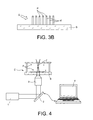
- FIG. 4 represents a first example of a device which implements the method of positioned growth of nanowires described in FIGS. 1A-1F ;
- FIG. 5 represents a second example of a device which implements the method of positioned growth of nanowires described in FIGS. 1A-1F ;
- FIGS. 6A-6C represent an example of positioned growth of nanowires on a solid immersion lens in accordance with the invention.
- FIG. 7 represents, as an example, a particular step of the method of positioned growth of nanowires on a solid immersion lens in accordance with the invention.
- FIGS. 1A-1F represent successive steps of a method for positioned growth of nanowires on a substrate.
- the optical clip is a light beam waist formed using a microscope objective the numerical aperture of which is greater than 1.
- the light beam from which the waist is formed is preferentially a laser beam.
- Metal nanoparticles P are placed in a tank C containing a fluid, for example a liquid L.
- the bottom of the tank C consists of a semiconductor substrate S.
- An cover glass La constitutes, for example, a lid closing the tank.
- the face of the semiconductor substrate intended to be in contact with the liquid L has preferentially previously been cleaned by a known method, for example a method of the oxygen plasma treatment type.
- a surface treatment T for example a treatment using poly-L-lysine or treatment by aminosilane, covers the face of the semiconductor substrate which is in contact with the liquid in order to facilitate attachment of the particles.
- the optical clip is accomplished by the waist W of a highly concentrated light beam F.
- the optical clip enables the nanoparticles to be moved, one by one, as far as the surface of the substrate (cf. FIG. 1B ).
- a nanoparticle When a nanoparticle is positioned on the substrate it attaches to it due to the electrostatic forces present at the surface of the substrate (Van der Waals forces). If present, the surface treatment T facilitates this attachment.
- the nanoparticles then remain attached to the substrate even when there is no light beam.
- the step of displacement of nanoparticles is repeated for as many times as required in order to attach, in the desired spatial configuration, the desired quantity of particles (cf. FIG. 1C ).
- the tank C is then removed and the residues of liquid L are evaporated, by drying, whilst controlling the temperature and pressure conditions (cf. FIG. 1D ).
- the drying temperature may thus be equal to 35° C., and the pressure equal to 1 atmosphere.
- the semiconductor substrate S is then positioned in a growth apparatus (not represented in figures) and precursor gases G are introduced into the apparatus in order to initiate a process, known per se, for growth of the nanowires.
- the precursor gases are, for example, nitrous oxide N 2 O, or diethylzinc in the case of zinc oxide (Z n O) nanowires, and silane SiH 4 in the case of silicon nanowires (Si).
- the metal nanoparticles P and the surface treatment T are removed, for example by chemical etching (cf. FIG. 1F ).
- the abovementioned surface treatment T designates a single layer of organic molecules of a thickness of a few nanometers.
- the choice of organic molecules is appropriate for the nature of the nano-objects to be created, and for the nature of the substrate S.
- the surface treatment is a treatment using poly-L-lysine.
- FIG. 2 represents an example of a device which implements the method of growth of nanowires illustrated in FIGS. 1A-1F .
- the fluid which fills the tank C is not a liquid but air A.
- the metal nanoparticles P are suspended in the air which fills the tank C using an aerosol.
- an atomiser N is used, for example, fitted with a network R of holes, agitated by ultrasound.
- the nanoparticles P are suspended in a solvent, for example ethanol, which fills the atomiser's tank.
- the nanoparticles P have a diameter less than the size of the holes, in order that they are able to traverse the network.
- An aperture in the exterior Ov is made in the tank C.
- the Ov aperture allows rapid evaporation of the solvent before a nanoparticle P which has entered into the tank arrives in the waist W of the beam F.
- the nanoparticles are thereby trapped in the air.
- the method of growth of nanowires is in accordance with the previously described method, except for the step of drying of the substrate, which in this case is advantageously unnecessary, as was mentioned above.
- FIGS. 3A-3B represent two steps of a variant of the method illustrated in FIGS. 1A-1F .
- the surface treatment T layer is removed before the growth of the nanowires, for example with a treatment under oxygen plasma PX.
- the surface treatment layer T is, in fact, a potentially contaminating layer between the substrate S and the metal nanoparticles P. Removal of the treatment layer T thus prevents all contamination and also allows a more uniform growth of the nanowires. It is thus possible to obtain nanowires the verticality of which relative to the substrate is very appreciably improved compared to a situation in which the layer T is retained during the growth of the nanowires (cf. FIG. 3B ).
- FIG. 4 represents a first example of a device which implements the method of positioned growth of nanowires.
- the multi-beam optical clip is created, in a manner known per se, by inserting an optical component 2 between the single light beam delivered by an optical source 1 and the tank C.
- the optical component 2 is, for example, a diffractive component, a holographic component or a component consisting of one or more spatial light modulators.
- the optical component 2 may be controlled, for example by a computer 4 .
- FIG. 5 illustrates a second example of a device which implements the method of positioned growth of nanowires.
- Gold colloids P of diameter 50 nm are dissolved in ethanol.
- the colloids solution is placed in the tank of an atomiser N which enables the metal particles to be diffused in aerosol form.
- a thin layer T of poly-L-lysine is deposited on the surface of a microcrystalline silicon wafer S, to facilitate satisfactory attachment of the colloids to the surface.
- the walls of the tank C made of PDMS (Polydimethylsiloxane) are attached to the face of the wafer covered with the thin layer T.
- the tank is transparent at the wavelength of the laser used to produce the optical clip.
- the tank has a first aperture 01 in one side, in which is inserted the end of the fluid channel K.
- the fluid channel K connects the tank to the atomiser.
- the tank also has a second aperture 0 v which establishes a communication between the air present inside the tank and the outside air.
- the “tank+substrate” assembly is placed in the sample-holder of an inverted microscope.
- the microscope includes an immersion lens 3 having a numerical aperture of 1.25. This lens is used both for producing the optical clip and for observing the sample.
- a CCD camera 11 is placed behind the microscope lens for viewing the sample.
- the optical clip is produced by injecting in the lens 3 the light derived from a YAG laser 1 emitting, at wavelength 1064 nm, a power rating of 100 mW.
- the optical clip is first positioned, inside the tank, in the area of the output of the fluid channel, to await the arrival of a particle originating from the channel.
- the operator moves the optical clip and/or the tank in such a way as to place the particle at the desired position on the surface of the wafer.
- the particle remains attached to the surface, due to the poly-L-lysine.
- the process is repeated for as many times as required.
- the PDMS tank is then separated from the sample.
- the substrate is cleaned under oxygen plasma, and then placed in the chamber of an LPCVD (Low Pressure Chemical Vapour Deposition) apparatus.
- LPCVD Low Pressure Chemical Vapour Deposition
- the growth of the nanowires takes place by the VLS (Vapour-Liquid-Solid) method, by introducing silane (SiH 4 ) into the apparatus, at a rate of between 10 and 30 sccm and with a growth temperature of between 400 and 650° C.
- VLS Volt-Liquid-Solid
- FIGS. 6A-6C represent steps of an example of method for positioned growth of nanowires according to the invention.
- an optical clip is produced using a light beam which is highly focused by a solid immersion lens.
- a solid immersion lens is a lens, preferentially of hemispherical shape, which is manufactured using a material with a high refraction index n (2 ⁇ n). Use of such a lens enables the numerical aperture of the optical system to be increased and, by this means, the size of the focusing point to be reduced by a factor 1/n compared to the resolution limit in air.
- the device which implements the method of the invention thus includes a solid immersion lens 7 on the flat face of which a layer of a semiconductor material 9 is deposited.
- the layer of semiconductor material 9 is transparent at the operating wavelength and has a thickness which is small compared to this wavelength.
- the lens/layer assembly of semiconductor material is partially placed in a tank 8 filled with a liquid L which contains the metal particles P.
- the flat face of the lens 7 covered with the semiconductor layer is brought into contact with the liquid, with the remainder of the lens located outside the tank.
- the face of the semiconductor material in contact with the liquid L can be covered with the same surface treatment T (poly-L-lysine) as that described above.
- the lens is lit, on the hemispherical side, using a focused light beam I emanating from a microscope lens 5 with a low numerical aperture.
- a support 6 enables the lens 7 to be kept in contact with the liquid L.
- the tank 8 is moved until a particle P is positioned close to the centre of the lens 7 .
- the light focused around the lens/layer assembly of semiconductor material is used in this case as an optical clip to trap the particle in the same way as the abovementioned optical clip's laser beam waist.
- the particle P is attached to the layer 9 by electrostatic force. This attachment by electrostatic force depends on the surface condition of the particle and on the surface condition of the substrate.
- reference 10 represents, symbolically, the light intensity at the focus of the lens 7 .
- a step of growth of nanowire of then follows the attachment of the particle P to the substrate (cf. FIG. 6C ).
- FIG. 7 represents, as an example, a particular step of a variant of the method of positioned growth of nanowire of the invention.
- the metal nanoparticles are attached by fusion to the surface of the layer of semiconductor material 9 .
- a laser beam F 2 for example a laser beam of the Ultra Violet (UV) pulse type, is also focused on the layer of semiconductor material 9 .
- Beams F 1 and F 2 are then injected, via a semi-reflective blade 11 , in the same microscope objective Ob with high numerical aperture.
- a metal nanoparticle P which is conveyed and deposited on the layer of semiconductor material 9 using the optical clip, is then welded on this same layer using the focused pulse UV laser beam.
- a single nanoparticle P is attached to layer 9 .
- the invention concerns, however, other embodiments in which several nanoparticles are attached on layer 9 . Several nanoparticles are then trapped in the same focused beam.
- nanoparticle is used to designate, generally, all particles of small dimensions, able to be positioned, as a catalyst, on the substrate.
- the term “nanoparticle” must not, of course, be understood as an object with dimensions exclusively of the order of a few nanometers. The dimensions of the “nanoparticles” can thus be between several nanometers and several tens of micrometers.
Landscapes
- Chemical & Material Sciences (AREA)
- Engineering & Computer Science (AREA)
- Crystallography & Structural Chemistry (AREA)
- Materials Engineering (AREA)
- Metallurgy (AREA)
- Organic Chemistry (AREA)
- Silicon Compounds (AREA)
- Crystals, And After-Treatments Of Crystals (AREA)
Applications Claiming Priority (3)
| Application Number | Priority Date | Filing Date | Title |
|---|---|---|---|
| FR0950573A FR2941688B1 (fr) | 2009-01-30 | 2009-01-30 | Procede de formation de nano-fils |
| FR0950573 | 2009-01-30 | ||
| PCT/EP2010/051012 WO2010086378A1 (fr) | 2009-01-30 | 2010-01-28 | Procede de formation de nano-fils et procede de fabrication de composant optique associe |
Publications (2)
| Publication Number | Publication Date |
|---|---|
| US20120021554A1 US20120021554A1 (en) | 2012-01-26 |
| US8569151B2 true US8569151B2 (en) | 2013-10-29 |
Family
ID=40792591
Family Applications (1)
| Application Number | Title | Priority Date | Filing Date |
|---|---|---|---|
| US13/147,081 Expired - Fee Related US8569151B2 (en) | 2009-01-30 | 2010-01-28 | Method of formation of nanowires and method of manufacture of associated optical component |
Country Status (5)
| Country | Link |
|---|---|
| US (1) | US8569151B2 (ja) |
| EP (1) | EP2391578B1 (ja) |
| JP (1) | JP5680552B2 (ja) |
| FR (1) | FR2941688B1 (ja) |
| WO (1) | WO2010086378A1 (ja) |
Families Citing this family (11)
| Publication number | Priority date | Publication date | Assignee | Title |
|---|---|---|---|---|
| GB201021112D0 (en) | 2010-12-13 | 2011-01-26 | Ntnu Technology Transfer As | Nanowires |
| GB201200355D0 (en) * | 2012-01-10 | 2012-02-22 | Norwegian Univ Sci & Tech Ntnu | Nanowires |
| GB201211038D0 (en) | 2012-06-21 | 2012-08-01 | Norwegian Univ Sci & Tech Ntnu | Solar cells |
| US10179952B2 (en) * | 2013-03-08 | 2019-01-15 | Rutgers, The State University Of New Jersey | Patterned thin films by thermally induced mass displacement |
| GB201311101D0 (en) | 2013-06-21 | 2013-08-07 | Norwegian Univ Sci & Tech Ntnu | Semiconducting Films |
| KR102564288B1 (ko) | 2015-07-13 | 2023-08-04 | 크래요나노 에이에스 | 그라파이트 기판상에서 성장한 나노와이어 또는 나노피라미드 |
| KR20180055803A (ko) | 2015-07-13 | 2018-05-25 | 크래요나노 에이에스 | 나노와이어/나노피라미드 형상 발광 다이오드 및 광검출기 |
| EA201890238A1 (ru) | 2015-07-31 | 2018-08-31 | Крайонано Ас | Способ выращивания нанопроволок или нанопирамидок на графитовых подложках |
| GB201705755D0 (en) | 2017-04-10 | 2017-05-24 | Norwegian Univ Of Science And Tech (Ntnu) | Nanostructure |
| US10203938B2 (en) * | 2017-04-21 | 2019-02-12 | Accenture Global Solutions Limited | Application engineering platform |
| GB201913701D0 (en) | 2019-09-23 | 2019-11-06 | Crayonano As | Composition of matter |
Citations (13)
| Publication number | Priority date | Publication date | Assignee | Title |
|---|---|---|---|---|
| WO2004004927A2 (en) | 2002-07-08 | 2004-01-15 | Btg International Limited | Nanostructures and methods for manufacturing the same |
| US20040036976A1 (en) * | 2001-04-27 | 2004-02-26 | University Of Chicago | Apparatus for using optical tweezers to manipulate materials |
| US20040082178A1 (en) | 2002-10-28 | 2004-04-29 | Kamins Theodore I. | Method of forming catalyst nanoparticles for nanowire growth and other applications |
| US20050112048A1 (en) * | 2003-11-25 | 2005-05-26 | Loucas Tsakalakos | Elongated nano-structures and related devices |
| US20050122550A1 (en) | 2003-10-28 | 2005-06-09 | Joseph Plewa | System and method for manipulating and processing materials using holographic optical trapping |
| US20050151126A1 (en) | 2003-12-31 | 2005-07-14 | Intel Corporation | Methods of producing carbon nanotubes using peptide or nucleic acid micropatterning |
| US20060286023A1 (en) * | 2004-08-02 | 2006-12-21 | Houjin Huang | Carbon nanotube, method for positioning the same, field-effect transistor made using the carbon nanotube, method for making the field-effect transistor, and semiconductor device |
| US20070069119A1 (en) * | 2005-09-23 | 2007-03-29 | Massachusetts Institute Of Technology | Optical trapping with a semiconductor |
| GB2436449A (en) | 2003-11-25 | 2007-09-26 | Gen Electric | Method of making a field emission device |
| US20080190756A1 (en) * | 2003-12-04 | 2008-08-14 | Commissariat A L'energie Atomique | Object Separation Device Using Optical Method |
| US20080191317A1 (en) | 2007-02-13 | 2008-08-14 | International Business Machines Corporation | Self-aligned epitaxial growth of semiconductor nanowires |
| US20080315175A1 (en) * | 2005-12-30 | 2008-12-25 | The Regents Of The University Of California | Alignment, transportation and integration of nanowires using optical trapping |
| FR2924855A1 (fr) * | 2008-05-26 | 2009-06-12 | Commissariat Energie Atomique | Procede de positionnement de particule dans une zone cible et dispositif associe |
Family Cites Families (1)
| Publication number | Priority date | Publication date | Assignee | Title |
|---|---|---|---|---|
| US8183566B2 (en) * | 2007-03-01 | 2012-05-22 | Hewlett-Packard Development Company, L.P. | Hetero-crystalline semiconductor device and method of making same |
-
2009
- 2009-01-30 FR FR0950573A patent/FR2941688B1/fr not_active Expired - Fee Related
-
2010
- 2010-01-28 WO PCT/EP2010/051012 patent/WO2010086378A1/fr not_active Ceased
- 2010-01-28 US US13/147,081 patent/US8569151B2/en not_active Expired - Fee Related
- 2010-01-28 EP EP10701373A patent/EP2391578B1/fr not_active Not-in-force
- 2010-01-28 JP JP2011546846A patent/JP5680552B2/ja not_active Expired - Fee Related
Patent Citations (16)
| Publication number | Priority date | Publication date | Assignee | Title |
|---|---|---|---|---|
| US20040036976A1 (en) * | 2001-04-27 | 2004-02-26 | University Of Chicago | Apparatus for using optical tweezers to manipulate materials |
| WO2004004927A2 (en) | 2002-07-08 | 2004-01-15 | Btg International Limited | Nanostructures and methods for manufacturing the same |
| US7335908B2 (en) * | 2002-07-08 | 2008-02-26 | Qunano Ab | Nanostructures and methods for manufacturing the same |
| US20080296785A1 (en) | 2002-10-28 | 2008-12-04 | Kamins Theodore I | Method of forming catalyst nanoparticles for nanowire growth and other applications |
| US20040082178A1 (en) | 2002-10-28 | 2004-04-29 | Kamins Theodore I. | Method of forming catalyst nanoparticles for nanowire growth and other applications |
| US20040079278A1 (en) | 2002-10-28 | 2004-04-29 | Kamins Theodore I. | Method of forming three-dimensional nanocrystal array |
| US20050122550A1 (en) | 2003-10-28 | 2005-06-09 | Joseph Plewa | System and method for manipulating and processing materials using holographic optical trapping |
| US20050112048A1 (en) * | 2003-11-25 | 2005-05-26 | Loucas Tsakalakos | Elongated nano-structures and related devices |
| GB2436449A (en) | 2003-11-25 | 2007-09-26 | Gen Electric | Method of making a field emission device |
| US20080190756A1 (en) * | 2003-12-04 | 2008-08-14 | Commissariat A L'energie Atomique | Object Separation Device Using Optical Method |
| US20050151126A1 (en) | 2003-12-31 | 2005-07-14 | Intel Corporation | Methods of producing carbon nanotubes using peptide or nucleic acid micropatterning |
| US20060286023A1 (en) * | 2004-08-02 | 2006-12-21 | Houjin Huang | Carbon nanotube, method for positioning the same, field-effect transistor made using the carbon nanotube, method for making the field-effect transistor, and semiconductor device |
| US20070069119A1 (en) * | 2005-09-23 | 2007-03-29 | Massachusetts Institute Of Technology | Optical trapping with a semiconductor |
| US20080315175A1 (en) * | 2005-12-30 | 2008-12-25 | The Regents Of The University Of California | Alignment, transportation and integration of nanowires using optical trapping |
| US20080191317A1 (en) | 2007-02-13 | 2008-08-14 | International Business Machines Corporation | Self-aligned epitaxial growth of semiconductor nanowires |
| FR2924855A1 (fr) * | 2008-05-26 | 2009-06-12 | Commissariat Energie Atomique | Procede de positionnement de particule dans une zone cible et dispositif associe |
Non-Patent Citations (3)
| Title |
|---|
| French Preliminary Search Report issued Jul. 3, 2009, in Patent Application No. 0950573. |
| Maria Dienerowitz, et al., "Optical manipulation of nanoparticles: a review", Journal of Nanophotonics, vol. 2, No. 021875, XP 40447263, Sep. 10, 2008, pp. 1-31. |
| Yi Cui, et al., "Diameter-controlled synthesis of single-crystal silicon nanowires", Applied Physics Letters, vol. 78, No. 15, XP 2535075, Apr. 9, 2011, pp. 2214-2216. |
Also Published As
| Publication number | Publication date |
|---|---|
| FR2941688B1 (fr) | 2011-04-01 |
| WO2010086378A1 (fr) | 2010-08-05 |
| EP2391578A1 (fr) | 2011-12-07 |
| FR2941688A1 (fr) | 2010-08-06 |
| EP2391578B1 (fr) | 2013-01-02 |
| US20120021554A1 (en) | 2012-01-26 |
| JP5680552B2 (ja) | 2015-03-04 |
| JP2012516242A (ja) | 2012-07-19 |
Similar Documents
| Publication | Publication Date | Title |
|---|---|---|
| US8569151B2 (en) | Method of formation of nanowires and method of manufacture of associated optical component | |
| EP1613549B1 (en) | Precisely positioned nanowhisker structures and method for preparing them | |
| Kojima et al. | Nanoparticle formation in Au thin films by electron-beam-induced dewetting | |
| JP2012516242A5 (ja) | ||
| Li et al. | Large-area well-ordered nanodot array pattern fabricated with self-assembled nanosphere template | |
| CN113649584B (zh) | 一种激光诱导形貌可控的金或金复合纳米结构的生长方法及其应用 | |
| Zhao et al. | Laser additive nano-manufacturing under ambient conditions | |
| US20030143327A1 (en) | Method for producing a carbon nanotube | |
| CN109119332B (zh) | 一种采用退火方法制备图案化有序双金属纳米粒子阵列的方法 | |
| Yoshimoto et al. | In-process sintering of Au nanoparticles deposited in laser-assisted electrophoretic deposition | |
| WO2008045114A9 (en) | Method for fabricating nanostructures | |
| US20110101211A1 (en) | Device for trapping particles | |
| Lewandowski et al. | Nanostructures of cysteine-coated CdS nanoparticles produced with “two-particle” lithography | |
| EP2024768B1 (de) | Verfahren zur herstellung eines photonischen kristalls | |
| CN101975976B (zh) | 基于金属纳米颗粒的光子晶体微纳结构直写方法 | |
| Sachan et al. | Laser‐induced self‐assembled nanostructures on electron‐transparent substrates | |
| JP4024532B2 (ja) | 微粒子配列膜形成方法 | |
| KR100803053B1 (ko) | 주기적인 패턴을 갖는 산화아연 나노막대 어레이의제조방법 | |
| JP2010208925A (ja) | 半導体ナノワイヤの製造方法及び半導体装置 | |
| Zywietz et al. | Laser printing of nanoparticles | |
| US20090269495A1 (en) | Method for Producing Nanostructures on a Substrate | |
| Farzinpour | Dynamic templating: A new pathway for the assembly of large-area arrays of plasmonic, magnetic and semiconductor nanomaterials | |
| Delaporte et al. | The surface nanostructurations by means of near field enhancement with nanospheres | |
| Zacharias et al. | From Ordered Arrays of Nanowires to Controlled Solid State Reactions | |
| Gheorghe et al. | INTELLIGENT MICRO-NANO-FABRICATION |
Legal Events
| Date | Code | Title | Description |
|---|---|---|---|
| AS | Assignment |
Owner name: COMMISSARIAT A L'ENERGIE ATOMIQUE ET AUX ENERGIES Free format text: ASSIGNMENT OF ASSIGNORS INTEREST;ASSIGNORS:NEEL, DELPHINE;FERRET, PIERRE;GETIN, STEPHANE;REEL/FRAME:027048/0282 Effective date: 20110929 |
|
| STCF | Information on status: patent grant |
Free format text: PATENTED CASE |
|
| FPAY | Fee payment |
Year of fee payment: 4 |
|
| FEPP | Fee payment procedure |
Free format text: MAINTENANCE FEE REMINDER MAILED (ORIGINAL EVENT CODE: REM.); ENTITY STATUS OF PATENT OWNER: LARGE ENTITY |
|
| LAPS | Lapse for failure to pay maintenance fees |
Free format text: PATENT EXPIRED FOR FAILURE TO PAY MAINTENANCE FEES (ORIGINAL EVENT CODE: EXP.); ENTITY STATUS OF PATENT OWNER: LARGE ENTITY |
|
| STCH | Information on status: patent discontinuation |
Free format text: PATENT EXPIRED DUE TO NONPAYMENT OF MAINTENANCE FEES UNDER 37 CFR 1.362 |
|
| FP | Lapsed due to failure to pay maintenance fee |
Effective date: 20211029 |