US8410485B2 - Pixel structure - Google Patents
Pixel structure Download PDFInfo
- Publication number
- US8410485B2 US8410485B2 US13/080,664 US201113080664A US8410485B2 US 8410485 B2 US8410485 B2 US 8410485B2 US 201113080664 A US201113080664 A US 201113080664A US 8410485 B2 US8410485 B2 US 8410485B2
- Authority
- US
- United States
- Prior art keywords
- gate
- drain
- pixel electrode
- source
- pixel structure
- Prior art date
- Legal status (The legal status is an assumption and is not a legal conclusion. Google has not performed a legal analysis and makes no representation as to the accuracy of the status listed.)
- Expired - Fee Related, expires
Links
- 239000004065 semiconductor Substances 0.000 claims abstract description 20
- 239000012212 insulator Substances 0.000 claims description 9
- 239000000463 material Substances 0.000 claims description 5
- 239000004020 conductor Substances 0.000 claims description 3
- 101100489584 Solanum lycopersicum TFT1 gene Proteins 0.000 description 11
- 101100214488 Solanum lycopersicum TFT2 gene Proteins 0.000 description 10
- 239000004973 liquid crystal related substance Substances 0.000 description 5
- 230000009977 dual effect Effects 0.000 description 4
- 239000010408 film Substances 0.000 description 4
- 239000000758 substrate Substances 0.000 description 4
- 238000005516 engineering process Methods 0.000 description 3
- 238000004519 manufacturing process Methods 0.000 description 3
- 230000008901 benefit Effects 0.000 description 2
- 239000010409 thin film Substances 0.000 description 2
- 230000015572 biosynthetic process Effects 0.000 description 1
- 230000005684 electric field Effects 0.000 description 1
- 238000000034 method Methods 0.000 description 1
- 238000012986 modification Methods 0.000 description 1
- 230000004048 modification Effects 0.000 description 1
- OFIYHXOOOISSDN-UHFFFAOYSA-N tellanylidenegallium Chemical compound [Te]=[Ga] OFIYHXOOOISSDN-UHFFFAOYSA-N 0.000 description 1
Images


Classifications
-
- G—PHYSICS
- G02—OPTICS
- G02F—OPTICAL DEVICES OR ARRANGEMENTS FOR THE CONTROL OF LIGHT BY MODIFICATION OF THE OPTICAL PROPERTIES OF THE MEDIA OF THE ELEMENTS INVOLVED THEREIN; NON-LINEAR OPTICS; FREQUENCY-CHANGING OF LIGHT; OPTICAL LOGIC ELEMENTS; OPTICAL ANALOGUE/DIGITAL CONVERTERS
- G02F1/00—Devices or arrangements for the control of the intensity, colour, phase, polarisation or direction of light arriving from an independent light source, e.g. switching, gating or modulating; Non-linear optics
- G02F1/01—Devices or arrangements for the control of the intensity, colour, phase, polarisation or direction of light arriving from an independent light source, e.g. switching, gating or modulating; Non-linear optics for the control of the intensity, phase, polarisation or colour
- G02F1/13—Devices or arrangements for the control of the intensity, colour, phase, polarisation or direction of light arriving from an independent light source, e.g. switching, gating or modulating; Non-linear optics for the control of the intensity, phase, polarisation or colour based on liquid crystals, e.g. single liquid crystal display cells
- G02F1/133—Constructional arrangements; Operation of liquid crystal cells; Circuit arrangements
- G02F1/136—Liquid crystal cells structurally associated with a semi-conducting layer or substrate, e.g. cells forming part of an integrated circuit
- G02F1/1362—Active matrix addressed cells
- G02F1/1368—Active matrix addressed cells in which the switching element is a three-electrode device
-
- H—ELECTRICITY
- H01—ELECTRIC ELEMENTS
- H01L—SEMICONDUCTOR DEVICES NOT COVERED BY CLASS H10
- H01L27/00—Devices consisting of a plurality of semiconductor or other solid-state components formed in or on a common substrate
- H01L27/02—Devices consisting of a plurality of semiconductor or other solid-state components formed in or on a common substrate including semiconductor components specially adapted for rectifying, oscillating, amplifying or switching and having potential barriers; including integrated passive circuit elements having potential barriers
- H01L27/12—Devices consisting of a plurality of semiconductor or other solid-state components formed in or on a common substrate including semiconductor components specially adapted for rectifying, oscillating, amplifying or switching and having potential barriers; including integrated passive circuit elements having potential barriers the substrate being other than a semiconductor body, e.g. an insulating body
- H01L27/1214—Devices consisting of a plurality of semiconductor or other solid-state components formed in or on a common substrate including semiconductor components specially adapted for rectifying, oscillating, amplifying or switching and having potential barriers; including integrated passive circuit elements having potential barriers the substrate being other than a semiconductor body, e.g. an insulating body comprising a plurality of TFTs formed on a non-semiconducting substrate, e.g. driving circuits for AMLCDs
- H01L27/124—Devices consisting of a plurality of semiconductor or other solid-state components formed in or on a common substrate including semiconductor components specially adapted for rectifying, oscillating, amplifying or switching and having potential barriers; including integrated passive circuit elements having potential barriers the substrate being other than a semiconductor body, e.g. an insulating body comprising a plurality of TFTs formed on a non-semiconducting substrate, e.g. driving circuits for AMLCDs with a particular composition, shape or layout of the wiring layers specially adapted to the circuit arrangement, e.g. scanning lines in LCD pixel circuits
Definitions
- the invention relates to a pixel structure, and more particularly to a pixel structure having dual active devices.
- the technologies that have been developed to satisfy the requirement of wide viewing angle include: twisted nematic (TN) LCD equipped with wide viewing films, in-plane switching (IPS) LCD, fringe field switching (FFS) LCD and multi-domain vertically alignment (MVA) LCD.
- TN twisted nematic
- IPS in-plane switching
- FFS fringe field switching
- MVA multi-domain vertically alignment
- the MVA-LCD since the alignment protrusions or slits formed on the color filter substrate or the thin film transistor (TFT) array substrate render the liquid crystal molecules arranged in multi-direction thereby obtaining a plurality of different aligned domains, the MVA-LCD meets the requirement of wide viewing angle.
- the MVA-LCD facilitates the requirement of wide viewing angle through the design of multi-domains
- the image brightness displayed by the MVA-LCD may not be uniformed if the viewing angle changes. Therefore, the problem such as color shift and the like is caused in the MVA-LCD.
- the technologies are mainly stands at the formation of different electric fields in two pixel electrodes of a single pixel unit. Accordingly, the liquid crystal molecules located above different pixel electrodes are arranged in different alignments to mitigate the color shift.
- the invention directed to a pixel structure to solve the color shift problem in an MVA-LCD.
- the invention provides a pixel structure including a scan line, a data line, a first gate, a second gate, a third gate, a semiconductor layer, a source, a first drain, a second drain, a first pixel electrode, and a second pixel electrode.
- the scan line has a mainline and a branch.
- the data line is intersected with the mainline.
- the semiconductor layer is disposed on the mainline and the branch to respectively define a first gate and a second gate.
- the source is directly connected to the data line.
- the source is disposed on the semiconductor layer and located between the first gate and the second gate.
- the first drain contacts the semiconductor layer, and the first gate is located between the first drain and the source.
- the second drain contacts the semiconductor layer, and the second gate is located between the second drain and the source.
- the third gate is electrically connected to the scan line.
- the first pixel electrode is electrically connected to the first drain.
- the second pixel electrode is electrically connected to the second drain.
- the pixel structure of the invention is configured with two active devices, wherein one of the active devices has two gates so that the two active devices have different property. Accordingly, under a same driving signal, a single pixel can be provided with different voltages. Therefore, when the pixel structure of the invention is applied in an MVA-LCD, the problem of color shift is eliminated.
- the dual gates active device is manufactured by the conventional process so that the manufacturing process and the material cost are not increased in the invention.
- FIG. 1A illustrates a schematic top view of a pixel structure according to an embodiment of the invention.
- FIG. 1B is a cross-sectional view taken along a section line I-I′ depicted in FIG. 1A .
- FIG. 1C is a cross-sectional view taken along a sectional line II-II′ depicted in FIG. 1A .
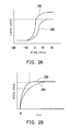
- FIG. 2A shows relationships between the driving voltage and the channel current of the first active device and the second active device in the pixel structure according to an embodiment of the invention.
- FIG. 2B shows relationships between the turn-on time and the writing voltages of the first active device and the second active device in the pixel structure according to an embodiment of the invention.
- FIG. 1A illustrates a schematic top view of a pixel structure according to an embodiment of the invention.
- a pixel structure 100 includes a scan line 110 , a first gate 116 , a second gate 118 , a data line 122 , a source 124 , a first drain 126 , a second drain 128 , a semiconductor layer 130 , a third gate 142 , a first pixel electrode 144 , and a second pixel electrode 146 .
- the scan line 110 has a mainline 112 and a branch 114 substantially parallel to the mainline 112 .
- the data line 122 is intersected with the mainline 112 .
- the semiconductor layer 130 crosses over the mainline 112 and the branch 114 to respectively define the first gate 116 and the second gate 118 . That is to say, the first gate 116 and the second gate 118 are the extension portions of the scan line 110 .
- the first gate 116 is disposed between the first drain 126 and the source 124 .
- the second gate 118 is disposed between the second drain 128 and the source 124 .
- the scan line 110 in the present embodiment has a protruding portion B connected between the branch 114 and the mainline 112 so that the first gate 116 and the second gate 118 are electrically connected.
- the scan line 116 is not restricted in the pattern design depicted herein. In other embodiments, the scan line 110 can have other pattern designs to define the corresponding first gate 116 and the corresponding second gate 118 .
- the source 124 is directly connected to the data line 122 , and located between the first gate 116 and the second gate 118 .
- the source 124 is an extension of the data line 122 and is exemplified located between the protruding portion B and the data line 120 . Nevertheless, the pattern of the source 124 is not restricted and the pattern of the source 124 can be designed and modified based on different requirements in other embodiments.
- the third gate 142 is located between the source 124 and the first drain 126 .
- the first pixel electrode 144 and the second pixel electrode 146 are respectively located at two opposite sides of the mainline 112 .
- FIG. 1B is a cross-sectional view taken along a section line I-I′ depicted in FIG. 1A .
- the pixel structure 100 is formed by a plurality of film layers sequentially disposed on a substrate 10 , wherein the film layers includes a first conductive layer (not shown), a first insulator layer 12 , the semiconductor layer 130 , a second conductive layer (not shown), a second insulator layer 14 , and a third conductive layer (not shown) in sequence.
- the first conductive layer (not shown) forms the scan line 110 , the first gate 116 , and the second gate 118 .
- the second conductive layer (not shown) forms the data line 122 , the source 124 , the first drain 126 , and the second drain 128 .
- the third conductive layer (not shown) forms the third gate 142 , the first pixel electrode 144 , and the second pixel electrode 146 .
- the third gate 142 is formed by one of the film layers most away from the substrate 10 , and thus a part of the semiconductor layer 130 is sandwiched between the first gate 116 and the third gate 142 in the cross sectional view. It is noted that the third gate 142 , the first pixel electrode 144 , and the second pixel electrode 146 are formed by the same material such as a transparent conductive material or other conductive materials. Hence, no additional cost or manufacturing process is needed for facilitating the disposition of the third gate 142 . In addition, the source 124 , the first drain 126 , and the second drain 128 all directly contact the semiconductor layer 130 .
- the first gate 116 , the third gate 142 , the semiconductor layer 130 , the source 124 , and the first drain 126 form a first active device TFT 1 .
- the second gate 118 , the semiconductor layer 130 , the source 124 , and the second drain 128 form a second active device TFT 2 .
- FIG. 1C is a cross-sectional view taken along a sectional line II-II′ depicted in FIG. 1A .
- the first insulator layer 12 in the present embodiment has a first gate contacting opening C 1 to partially expose the scan line 112 .
- the second insulator layer 14 has a second gate contacting opening C 2 , a first drain contacting opening C 3 , and a second drain contacting opening C 4 .
- the second gate contacting opening C 2 is disposed aligned to the first gate contacting opening C 1 such that the third gate 142 is electrically connected to the scan line 110 through the first gate contacting opening C 1 and the second gate contacting opening C 2 .
- first drain contacting opening C 3 partially expose the first drain 126 and the second drain contacting opening C 4 partially expose the second drain 128 . Therefore, the first pixel electrode 144 is electrically connected to the first drain 126 through the first drain contacting opening C 3 . Similarly, the second pixel electrode 146 is electrically connected to the second drain 128 through the second drain contacting opening C 4 .
- the third gate 142 is electrically connected to the scan line 110 so that the third gate 142 has a voltage the same as the voltage of the first gate 116 and the second gate 118 . Accordingly, the first active device TFT 1 is a dual gates thin film transistor and the second active device TFT 2 is a single gate thin film transistor. Under the disposition layout, the first active device TFT 1 and the second active device TFT 2 have different properties.
- FIG. 2A shows relationships between the driving voltage and the channel current of the first active device and the second active device in the pixel structure according to an embodiment of the invention
- FIG. 2B shows relationships between the turn-on time and the writing voltages of the first active device and the second active device in the pixel structure according to an embodiment of the invention.
- the curve 210 shows a relationship between the driving voltage and the channel current of the first active device TFT 1
- the curve 220 shows a relationship between the driving voltage and the channel current of the second active device TFT 2
- the curve 230 shows a relationship between the turn-on time and the writing voltages of the first active device TFT 1
- the curve 240 shows a relationship between the turn-on time and the writing voltages of the second active device TFT 2 .
- the first active device TFT 1 having dual gates has higher channel current.
- the second active device TFT 220 requires relative long time to completely write the predetermined voltage into the second pixel electrode 146 .
- the writing efficiency of the first active device TFT 1 is higher than that of the second active device TFT 2 .
- the pixel structure 100 can make the first pixel electrode 144 and the second pixel electrode 146 be written by different voltages under the same driving signal through properly control the turn-on time. Therefore, when the pixel structure 100 of the invention is applied in an MVA-LCD, the problem of color shift is eliminated.
- the scan line 110 transmits a turn-on voltage to turn on the first active device TFT 1 and the second active device TFT 2 when the pixel structure 100 is driven. Meanwhile, a data voltage transmitted by the data line 122 can be written into the first pixel electrode 144 and the second pixel electrode 146 respectively through the first active device TFT 1 and the second active device TFT 2 . Thereafter, the scan line 110 transmits a turn-off voltage to turn off the first active device TFT 1 and the second active device TFT 2 so that the writing action is terminated. Based on the relationships shown in FIG. 2B , the writing efficiency of the first active device TFT 1 differs from that of the second active device TFT 2 .
- the first pixel electrode 144 can be written in a higher voltage than that of the second pixel electrode 146 by properly controlling the turn-on time.
- the liquid crystal molecules located above the first pixel electrode 144 are arranged in the alignment different than the liquid crystal molecules located above the second pixel electrode 146 , thereby the problem of color shift is mitigated.
- the pixel structure of the invention makes the first pixel electrode and the second pixel electrode be written in different voltages by using the disposition of the third gate to solve the problem of color shift in an MVA-LCD.
- the third gate, the first pixel electrode, and the second pixel electrode are made by the same conductive layer without increasing the manufacturing process or the material cost.
- the disposition of the third gate would not decrease the aperture ratio of the pixel structure so that the pixel structure has quite good display quality.
Landscapes
- Physics & Mathematics (AREA)
- Engineering & Computer Science (AREA)
- Power Engineering (AREA)
- Microelectronics & Electronic Packaging (AREA)
- General Physics & Mathematics (AREA)
- Computer Hardware Design (AREA)
- Condensed Matter Physics & Semiconductors (AREA)
- Nonlinear Science (AREA)
- Mathematical Physics (AREA)
- Chemical & Material Sciences (AREA)
- Crystallography & Structural Chemistry (AREA)
- Optics & Photonics (AREA)
- Liquid Crystal (AREA)
- Thin Film Transistor (AREA)
Applications Claiming Priority (3)
| Application Number | Priority Date | Filing Date | Title |
|---|---|---|---|
| TW99110570A | 2010-04-06 | ||
| TW099110570A TWI402592B (zh) | 2010-04-06 | 2010-04-06 | 畫素結構 |
| TW99110570 | 2010-04-06 |
Publications (2)
| Publication Number | Publication Date |
|---|---|
| US20110241015A1 US20110241015A1 (en) | 2011-10-06 |
| US8410485B2 true US8410485B2 (en) | 2013-04-02 |
Family
ID=44708600
Family Applications (1)
| Application Number | Title | Priority Date | Filing Date |
|---|---|---|---|
| US13/080,664 Expired - Fee Related US8410485B2 (en) | 2010-04-06 | 2011-04-06 | Pixel structure |
Country Status (2)
| Country | Link |
|---|---|
| US (1) | US8410485B2 (zh) |
| TW (1) | TWI402592B (zh) |
Citations (5)
| Publication number | Priority date | Publication date | Assignee | Title |
|---|---|---|---|---|
| US20040085272A1 (en) * | 2002-11-01 | 2004-05-06 | Chin-Lung Ting | Multi-domain vertical alignment liquid crystal display and driving method thereof |
| US20070200989A1 (en) * | 2005-12-28 | 2007-08-30 | Lg.Philips Lcd Co., Ltd. | Liquid crystal display device and the method thereof |
| US20090096734A1 (en) * | 2007-10-12 | 2009-04-16 | Chi Mei Optoelectronics Corp. | Liquid crystal display and method of driving the same |
| US20090231505A1 (en) * | 2008-03-12 | 2009-09-17 | Chunghwa Picture Tubes, Ltd. | Multi-domain vertical alignment (mva) pixel structure |
| US20110049521A1 (en) * | 2009-09-01 | 2011-03-03 | Au Optronics Corporation | Active device array mother substrate and method of fabricating display panel |
Family Cites Families (2)
| Publication number | Priority date | Publication date | Assignee | Title |
|---|---|---|---|---|
| TWI364611B (en) * | 2007-10-05 | 2012-05-21 | Chimei Innolux Corp | Liquid crystal display |
| US8294840B2 (en) * | 2008-03-19 | 2012-10-23 | Chimei Innolux Corporation | Liquid crystal display device with fringe field switching mode |
-
2010
- 2010-04-06 TW TW099110570A patent/TWI402592B/zh not_active IP Right Cessation
-
2011
- 2011-04-06 US US13/080,664 patent/US8410485B2/en not_active Expired - Fee Related
Patent Citations (5)
| Publication number | Priority date | Publication date | Assignee | Title |
|---|---|---|---|---|
| US20040085272A1 (en) * | 2002-11-01 | 2004-05-06 | Chin-Lung Ting | Multi-domain vertical alignment liquid crystal display and driving method thereof |
| US20070200989A1 (en) * | 2005-12-28 | 2007-08-30 | Lg.Philips Lcd Co., Ltd. | Liquid crystal display device and the method thereof |
| US20090096734A1 (en) * | 2007-10-12 | 2009-04-16 | Chi Mei Optoelectronics Corp. | Liquid crystal display and method of driving the same |
| US20090231505A1 (en) * | 2008-03-12 | 2009-09-17 | Chunghwa Picture Tubes, Ltd. | Multi-domain vertical alignment (mva) pixel structure |
| US20110049521A1 (en) * | 2009-09-01 | 2011-03-03 | Au Optronics Corporation | Active device array mother substrate and method of fabricating display panel |
Also Published As
| Publication number | Publication date |
|---|---|
| US20110241015A1 (en) | 2011-10-06 |
| TWI402592B (zh) | 2013-07-21 |
| TW201135332A (en) | 2011-10-16 |
Similar Documents
| Publication | Publication Date | Title |
|---|---|---|
| JP5246782B2 (ja) | 液晶装置および電子機器 | |
| US10663806B2 (en) | Curved liquid crystal display | |
| US8174636B2 (en) | Thin film transistor substrate and liquid crystal display having the same comprising a coupling capacitor as a voltage divider between a TFT and a data line | |
| US9329440B2 (en) | Pixel structure | |
| US9151994B2 (en) | Display panel | |
| US7782432B2 (en) | Liquid crystal display device having a pixel electrode structure and an alignment layer causing pixel regions to operate in both twisted nematic and vertical alignment modes | |
| US8576365B2 (en) | Display panel | |
| US7898624B2 (en) | Pixel array substrate and liquid crystal display | |
| TW200819836A (en) | Liquid crystal display panel | |
| US7884912B2 (en) | Liquid crystal display device | |
| US9423659B2 (en) | Array substrate, liquid crystal display panel, and display device | |
| US7782415B2 (en) | Active matrix subtrate, liquid crystal display panel and method of manufacturing the same | |
| JP5551553B2 (ja) | 液晶表示装置 | |
| US8610856B2 (en) | Liquid crystal display device | |
| KR100603829B1 (ko) | 프린지 필드 스위칭 모드 액정표시장치 | |
| JP2015138233A (ja) | 液晶表示装置 | |
| US8502947B2 (en) | Liquid crystal display device | |
| US8085354B2 (en) | Pixel structure with semiconductor of top-gate TFT extended over electrodes and liquid crystal display panel | |
| US7667805B2 (en) | Array substrate and display panel having the same | |
| KR100794892B1 (ko) | 수직배열형 액정 디스플레이 | |
| KR20050058105A (ko) | 프린지 필드 스위칭 모드 액정표시장치 및 그 제조방법 | |
| US8410485B2 (en) | Pixel structure | |
| KR20020044282A (ko) | 프린지 필드 구동 모드 액정 표시 장치 | |
| US20060250562A1 (en) | Liquid crystal display panel, active matrix substrate and fabricating mehod | |
| JP2008065212A (ja) | 液晶表示パネル |
Legal Events
| Date | Code | Title | Description |
|---|---|---|---|
| AS | Assignment |
Owner name: WINTEK CORPORATION, TAIWAN Free format text: ASSIGNMENT OF ASSIGNORS INTEREST;ASSIGNORS:LIU, CHIN-CHANG;CHAN, CHIEN-TING;SU, KUO-CHANG;REEL/FRAME:026098/0142 Effective date: 20110329 |
|
| STCF | Information on status: patent grant |
Free format text: PATENTED CASE |
|
| FEPP | Fee payment procedure |
Free format text: PAT HOLDER CLAIMS SMALL ENTITY STATUS, ENTITY STATUS SET TO SMALL (ORIGINAL EVENT CODE: LTOS); ENTITY STATUS OF PATENT OWNER: SMALL ENTITY |
|
| REMI | Maintenance fee reminder mailed | ||
| FPAY | Fee payment |
Year of fee payment: 4 |
|
| SULP | Surcharge for late payment | ||
| FEPP | Fee payment procedure |
Free format text: MAINTENANCE FEE REMINDER MAILED (ORIGINAL EVENT CODE: REM.); ENTITY STATUS OF PATENT OWNER: SMALL ENTITY |
|
| LAPS | Lapse for failure to pay maintenance fees |
Free format text: PATENT EXPIRED FOR FAILURE TO PAY MAINTENANCE FEES (ORIGINAL EVENT CODE: EXP.); ENTITY STATUS OF PATENT OWNER: SMALL ENTITY |
|
| STCH | Information on status: patent discontinuation |
Free format text: PATENT EXPIRED DUE TO NONPAYMENT OF MAINTENANCE FEES UNDER 37 CFR 1.362 |
|
| FP | Lapsed due to failure to pay maintenance fee |
Effective date: 20210402 |