US8334820B2 - Plasma display panel - Google Patents
Plasma display panel Download PDFInfo
- Publication number
- US8334820B2 US8334820B2 US11/931,735 US93173507A US8334820B2 US 8334820 B2 US8334820 B2 US 8334820B2 US 93173507 A US93173507 A US 93173507A US 8334820 B2 US8334820 B2 US 8334820B2
- Authority
- US
- United States
- Prior art keywords
- electrode
- display panel
- plasma display
- scan electrode
- sustain
- Prior art date
- Legal status (The legal status is an assumption and is not a legal conclusion. Google has not performed a legal analysis and makes no representation as to the accuracy of the status listed.)
- Expired - Fee Related, expires
Links
Images


Classifications
-
- H—ELECTRICITY
- H01—ELECTRIC ELEMENTS
- H01J—ELECTRIC DISCHARGE TUBES OR DISCHARGE LAMPS
- H01J11/00—Gas-filled discharge tubes with alternating current induction of the discharge, e.g. alternating current plasma display panels [AC-PDP]; Gas-filled discharge tubes without any main electrode inside the vessel; Gas-filled discharge tubes with at least one main electrode outside the vessel
- H01J11/20—Constructional details
- H01J11/50—Filling, e.g. selection of gas mixture
-
- H—ELECTRICITY
- H01—ELECTRIC ELEMENTS
- H01J—ELECTRIC DISCHARGE TUBES OR DISCHARGE LAMPS
- H01J11/00—Gas-filled discharge tubes with alternating current induction of the discharge, e.g. alternating current plasma display panels [AC-PDP]; Gas-filled discharge tubes without any main electrode inside the vessel; Gas-filled discharge tubes with at least one main electrode outside the vessel
- H01J11/20—Constructional details
- H01J11/34—Vessels, containers or parts thereof, e.g. substrates
-
- H—ELECTRICITY
- H01—ELECTRIC ELEMENTS
- H01J—ELECTRIC DISCHARGE TUBES OR DISCHARGE LAMPS
- H01J11/00—Gas-filled discharge tubes with alternating current induction of the discharge, e.g. alternating current plasma display panels [AC-PDP]; Gas-filled discharge tubes without any main electrode inside the vessel; Gas-filled discharge tubes with at least one main electrode outside the vessel
- H01J11/10—AC-PDPs with at least one main electrode being out of contact with the plasma
- H01J11/12—AC-PDPs with at least one main electrode being out of contact with the plasma with main electrodes provided on both sides of the discharge space
-
- H—ELECTRICITY
- H01—ELECTRIC ELEMENTS
- H01J—ELECTRIC DISCHARGE TUBES OR DISCHARGE LAMPS
- H01J11/00—Gas-filled discharge tubes with alternating current induction of the discharge, e.g. alternating current plasma display panels [AC-PDP]; Gas-filled discharge tubes without any main electrode inside the vessel; Gas-filled discharge tubes with at least one main electrode outside the vessel
- H01J11/20—Constructional details
- H01J11/22—Electrodes, e.g. special shape, material or configuration
-
- H—ELECTRICITY
- H01—ELECTRIC ELEMENTS
- H01J—ELECTRIC DISCHARGE TUBES OR DISCHARGE LAMPS
- H01J2211/00—Plasma display panels with alternate current induction of the discharge, e.g. AC-PDPs
- H01J2211/20—Constructional details
- H01J2211/22—Electrodes
- H01J2211/24—Sustain electrodes or scan electrodes
- H01J2211/245—Shape, e.g. cross section or pattern
-
- H—ELECTRICITY
- H01—ELECTRIC ELEMENTS
- H01J—ELECTRIC DISCHARGE TUBES OR DISCHARGE LAMPS
- H01J2211/00—Plasma display panels with alternate current induction of the discharge, e.g. AC-PDPs
- H01J2211/20—Constructional details
- H01J2211/22—Electrodes
- H01J2211/26—Address electrodes
-
- H—ELECTRICITY
- H01—ELECTRIC ELEMENTS
- H01J—ELECTRIC DISCHARGE TUBES OR DISCHARGE LAMPS
- H01J2211/00—Plasma display panels with alternate current induction of the discharge, e.g. AC-PDPs
- H01J2211/20—Constructional details
- H01J2211/34—Vessels, containers or parts thereof, e.g. substrates
- H01J2211/36—Spacers, barriers, ribs, partitions or the like
- H01J2211/366—Spacers, barriers, ribs, partitions or the like characterized by the material
-
- H—ELECTRICITY
- H01—ELECTRIC ELEMENTS
- H01J—ELECTRIC DISCHARGE TUBES OR DISCHARGE LAMPS
- H01J2211/00—Plasma display panels with alternate current induction of the discharge, e.g. AC-PDPs
- H01J2211/20—Constructional details
- H01J2211/34—Vessels, containers or parts thereof, e.g. substrates
- H01J2211/38—Dielectric or insulating layers
Definitions
- This document relates to a plasma display panel.
- the plasma display panel includes a phosphor layer inside discharge cells partitioned by barrier ribs and a plurality of electrodes.
- a driving signal is supplied to the electrodes, thereby generating a discharge inside the discharge cells.
- the driving signal generates a discharge inside the discharge cells
- a discharge gas filled inside the discharge cells generates vacuum ultraviolet rays, which thereby cause phosphors formed inside the discharge cells to emit light, thus displaying an image on the screen of the plasma display panel.
- a plasma display panel comprises a front substrate, a scan electrode and a sustain electrode that are positioned parallel to each other on the front substrate, an upper dielectric layer positioned on the scan electrode and the sustain electrode, a rear substrate on which an address electrode is positioned to intersect the scan electrode and the sustain electrode, a lower dielectric layer positioned on the address electrode, and a barrier rib that is positioned between the front substrate and the rear substrate and partitions a discharge cell, the barrier rib including lead (Pb) equal to or less than 1,000 ppm (parts per million), wherein a discharge gas is filled between the front substrate and the rear substrate and includes helium (He) of 9% to 42%.
- Pb lead
- He helium
- a plasma display panel comprises a front substrate, a scan electrode and a sustain electrode that are positioned parallel to each other on the front substrate, the scan electrode and the sustain electrode each having a single-layered structure, an upper dielectric layer positioned on the scan electrode and the sustain electrode, a rear substrate on which an address electrode is positioned to intersect the scan electrode and the sustain electrode, a lower dielectric layer positioned on the address electrode, and a barrier rib that is positioned between the front substrate and the rear substrate and partitions a discharge cell, the barrier rib including lead (Pb) equal to or less than 1,000 ppm, wherein a discharge gas is filled between the front substrate and the rear substrate arid includes helium (He) of 9% to 42%.
- Pb lead
- He helium
- a plasma display panel comprises a front substrate, a scan electrode and a sustain electrode that are positioned parallel to each other on the front substrate, an interval between the scan electrode and the sustain electrode ranging from 80 ⁇ m to 250 ⁇ m, an upper dielectric layer positioned on the scan electrode and the sustain electrode, a rear substrate on which an address electrode is positioned to intersect the scan electrode and the sustain electrode, a lower dielectric layer positioned on the address electrode, and a barrier rib that is positioned between the front substrate and the rear substrate and partitions a discharge cell, the barrier rib including lead equal to or less than 1,000 ppm, wherein a discharge gas is filled between the front substrate and the rear substrate and includes helium (He) of 9% to 42%.
- He helium
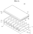
- FIGS. 1A to 1C illustrate a structure of a plasma display panel according to an exemplary embodiment
- FIG. 2 illustrates an operation of the plasma display panel according to the exemplary embodiment
- FIG. 3 illustrates a characteristic of the plasma display panel including helium (He);
- FIG. 4 illustrates a characteristic of the plasma display panel depending on a Pb content
- FIGS. 5A and 5B are graphs showing a consumption power and a luminance depending on a content of helium (He);
- FIGS. 6A and 6B are graphs showing a luminance and a firing voltage depending on a content of xenon (Xe);
- FIGS. 7A and 7B illustrate a scan electrode and a sustain electrode each having a single-layered structure
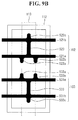
- FIG. 8A illustrates a scan electrode and a sustain electrode each having a multi-layered structure
- FIG. 8B illustrates a scan electrode and a sustain electrode each having a single-layered structure
- FIGS. 9A and 9B illustrate a structure of a scan electrode and a sustain electrode
- FIG. 10A illustrates a scan electrode and a sustain electrode each having a multi-layered structure
- FIG. 10B illustrates a scan electrode and a sustain electrode each having a single-layered structure:
- FIG. 11 is a diagram for explaining an interval between a scan electrode and a sustain electrode.
- FIG. 12 is a graph showing a luminance and a firing voltage depending on an interval between a scan electrode and a sustain electrode.
- FIGS. 1A to 1C illustrate a structure of a plasma display panel according to an exemplary embodiment.
- a plasma display panel 100 includes a front substrate 101 and a rear substrate 111 which coalesce with each other using a seal layer (not shown) to be opposite to each other.
- a scan electrode 102 and a sustain electrode 103 are positioned parallel to each other.
- an address electrode 113 is positioned to intersect the scan electrode 102 and the sustain electrode 103 .
- An upper dielectric layer 104 for covering the scan electrode 102 and the sustain electrode 103 is positioned on the front substrate 101 on which the scan electrode 102 and the sustain electrode 103 are positioned.
- the upper dielectric layer 104 limits discharge currents of the scan electrode 102 and the sustain electrode 103 , and provides electrical insulation between the scan electrode 102 and the sustain electrode 103 .
- a protective layer 105 is positioned on the upper dielectric layer 104 to facilitate discharge conditions.
- the protective layer 105 may include a material having a high secondary electron emission coefficient, for example, magnesium oxide (MgO).
- a lower dielectric layer 115 for covering the address electrode 113 is positioned on the rear substrate 111 on which the address electrode 113 is positioned.
- the lower dielectric layer 115 provides electrical insulation of the address electrodes 113 .
- Barrier ribs 112 of a stripe type, a well type, a delta type, a honeycomb type, and the like, are positioned on the lower dielectric layer 115 to partition discharge spaces (i.e., discharge cells).
- a red (R) discharge cell, a green (G) discharge cell, and a blue (B) discharge cell, and the like, may be positioned between the front substrate 101 and the rear substrate 111 .
- a white (W) discharge cell or a yellow (Y) discharge cell may be positioned.
- Each discharge cell partitioned by the barrier ribs 112 is filled with a discharge gas.
- a phosphor layer 114 is positioned inside the discharge cells to emit visible light for an image display during the generation of an address discharge.
- first, second and third phosphor layer respectively emitting red (R), green (G) and blue (B) light may be positioned inside the discharge cells.
- a phosphor layer emitting white (W) or yellow (Y) light may be positioned.
- a thickness of at least one of the phosphor layers 114 formed inside the red (R), green (G) and blue (B) discharge cells may be different from thicknesses of the other phosphor layers.
- thicknesses of the second and third phosphor layers inside the green (G) and blue (B) discharge cells may be larger than a thickness of the first phosphor layer inside the red (R) discharge cell.
- the thickness of the second phosphor layer may be substantially equal or different from the thickness of the third phosphor layer.
- Widths of the red (R), green (G), and blue (B) discharge cells may be substantially equal to one another. Further, a width of at least one of the red (R), green (G), or blue (B) discharge cells may be different from widths of the other discharge cells. For instance, a width of the red (R) discharge cell may be the smallest, and widths of the green (G) and blue (B) discharge cells may be larger than the width of the red (R) discharge cell. The width of the green (G) discharge cell may be substantially equal or different from the width of the blue (B) discharge cell.
- a width of the phosphor layer 114 positioned inside the discharge cell changes depending on the width of the discharge cell. For instance, a width of the second phosphor layer inside the green (G) discharge cell may be larger than a width of the first phosphor layer inside the red (R) discharge cell. Further, a width of the third phosphor layer inside the blue (B) discharge cell may be larger than the width of the first phosphor layer. Hence, a color temperature of an image displayed on the plasma display panel can be improved.
- the plasma display panel 100 may have various forms of barrier rib structures as well as a structure of the barrier rib 112 illustrated in FIG. 1A .
- the barrier rib 112 includes a first barrier rib 112 b and a second barrier rib 112 a .
- the barrier rib 112 may have a differential type barrier rib structure in which heights of the first and second barrier ribs 112 b and 112 a are different from each other.
- the height of the first barrier rib 112 b may be smaller than the height of the second barrier rib 112 a.
- FIG. 1A has been illustrated and described the case where the red (R), green (G) and blue (B) discharge cells are arranged on the same line
- the red (R), green (G) and blue (B) discharge cells may be arranged in a different pattern.
- a delta type arrangement in which the red (R), green (G), and blue (B) discharge cells are arranged in a triangle shape may be applicable.
- the discharge cells may have a variety of polygonal shapes such as pentagonal and hexagonal shapes as well as a rectangular shape.
- FIG. 1A has illustrated and described the case where the barrier rib 112 is formed on the rear substrate 111
- the barrier rib 112 may be formed on at least one of the front substrate 101 or the rear substrate 111 .
- the exemplary embodiment is not limited to the plasma display panel with the above-described structure.
- the above description illustrates a case where the upper dielectric layer 104 and the lower dielectric layer 115 each have a sing-layered structure, at least one of the upper dielectric layer 104 or the lower dielectric layer 115 may have a multi-layered structure.
- a width or thickness of the address electrode 113 inside the discharge cell may be different from a width or thickness of the address electrode 113 outside the discharge cell.
- a width or thickness of the address electrode 113 inside the discharge cell may be larger than a width or thickness of the address electrode 113 outside the discharge cell.
- the plasma display panel 100 may be divided into a first area 140 and a second area 150 .
- first address electrodes Xa 1 , Xa 1 , . . . Xam are positioned parallel to one another.
- second area 150 a plurality of second address electrodes Xb 1 , Xb 1 , . . . Xbm are positioned parallel to one another to be opposite to the plurality of first address electrodes Xa 1 , Xa 1 , . . . , Xam.
- FIG. 1C illustrates in detail an area A where the first address electrodes and the second address electrodes are opposite to each other.
- the first address electrodes Xa(m- 2 ), Xa(m- 1 ) and Xam are opposite to the second address electrodes Xb(m- 2 ), Xb(m- 1 ) and Xbm with a distance d therebetween, respectively.
- the distance d may range from about 50 ⁇ m to 300 ⁇ m. Further, the distance d may range from about 70 ⁇ m to 220 ⁇ m.
- FIG. 2 illustrates an operation of the plasma display panel according to the exemplary embodiment.
- the exemplary embodiment is not limited to FIG. 2 , and an operation method of the plasma display can be variously changed.
- a reset signal is supplied to the scan electrode.
- the reset signal includes a rising signal and a falling signal.
- the reset period is further divided into a setup period and a set-down period.
- the rising signal is supplied to the scan electrode.
- the rising signal sharply rises from a first voltage V 1 to a second voltage V 2 , and then gradually rises from the second voltage V 2 to a third voltage V 3 .
- the first voltage V 1 may be a ground level voltage GND.
- the rising signal generates a weak dark discharge (i.e., a setup discharge) inside the discharge cell during the setup period, thereby accumulating a proper amount of wall charges inside the discharge cell.
- a weak dark discharge i.e., a setup discharge
- a falling signal of a polarity direction opposite a polarity direction of the rising signal is supplied to the scan electrode.
- the falling signal gradually falls from a fourth voltage V 4 lower than a peak voltage (i.e., the third voltage V 3 ) of the rising signal to a fifth voltage V 5 .
- the falling signal generates a weak erase discharge (i.e., a set-down discharge) inside the discharge cell. Furthermore, the remaining wall charges are uniform inside the discharge cells to the extent that an address discharge can be stably performed.
- a scan bias signal which is maintained at a sixth voltage V 6 higher than a lowest voltage (i.e., the fifth voltage V 5 ) of the falling signal, is supplied to the scan electrode.
- a scan signal which falls from the scan bias signal by a scan voltage magnitude ⁇ Vy, is supplied to the scan electrode.
- a width of a scan signal supplied during an address period of at least one subfield may be different from a width of a scan signal supplied during address periods of the other subfields.
- a width of a scan signal in a subfield may be larger than a width of a scan signal in the next subfield in time order.
- a width of the scan signal may be gradually reduced in the order of 2.6 ⁇ s, 2.3 ⁇ s, 2.1 ⁇ s, 1.9 ⁇ s, etc., or in the order of 2.6 ⁇ s, 2.3 ⁇ s, 2.3 ⁇ s, 2.1 ⁇ s, . . . , 1.9 ⁇ s, 1.9 ⁇ s, etc.
- a data signal corresponding to the scan signal is supplied to the address electrode.
- the data signal rises from a ground level voltage GND by a data voltage magnitude ⁇ Vd.
- the address discharge occurs within the discharge cell to which the data signal is supplied.
- a sustain bias signal is supplied to the sustain electrode during the address period to prevent the generation of the unstable address discharge by interference of the sustain electrode Z.
- the sustain bias signal is substantially maintained at a sustain bias voltage Vz.
- the sustain bias voltage Vz is lower than a voltage Vs of a sustain signal and is higher than the ground level voltage GND.
- a sustain signal is alternately supplied to the scan electrode and the sustain electrode.
- the sustain signal has a voltage magnitude corresponding to the sustain voltage Vs.
- the sustain discharge i.e., a display discharge occurs between the scan electrode and the sustain electrode.
- a plurality of sustain signals are supplied during a sustain period of at least one subfield, and a width of at least one of the plurality of sustain signals may be different from widths of the other sustain signals. For instance, a width of a first supplied sustain signal among the plurality of sustain signals may be larger than widths of the other sustain signals. Hence, a sustain discharge can be more stable.
- a discharge gas filled inside the plasma display panel includes helium (He).
- the discharge gas may further include xenon (Xe) and neon (Ne).
- Helium (He) can lower a firing voltage, thereby improving the driving efficiency.
- FIG. 3 illustrates a characteristic of the plasma display panel including helium (He).
- FIG. 3 illustrates a consumption power, an efficiency, and a luminance of a displayed image of each of a case 1 of the plasma display panel including Ne of 85% and Xe of 15% as a discharge gas, a case 2 of the plasma display panel including Ne of 60%, Xe of 15% and He of 25% as a discharge gas, a case 3 of the plasma display panel including Ne of 90% and Xe of 10% as a discharge gas, and a case 4 of the plasma display panel including Ne of 65%m Xe of 10% and He of 25% as a discharge gas.
- a barrier rib in the cases 1 to 4 is formed of PbO—B 2 O 3 -SiO 2 glass.
- the barrier rib in the cases 1 to 4 includes lead (Pb) exceeding 1,000 ppm (parts per million), and is called an A-type barrier rib.
- FIG. 3 illustrates a consumption power, an efficiency, and a luminance of a displayed image of each of a case 5 having the same composition as the case 1 , a case 6 having the same composition as the case 2 , a case 7 having the same composition as the case 3 , and a case 8 having the same composition as the case 4 .
- a barrier rib in the cases 5 to 8 includes Pb equal to or less than 1,000 ppm, and is called a B-type barrier rib.
- a consumption power is 272 W
- an efficiency is 1.108 lm/W
- a luminance is 142 cd/m 2
- a consumption power is 257 W
- an efficiency is 1.33 lm/W
- a luminance is 125 cd/m 2 .
- the case 2 including He of 25% has the lower consumption power and the higher efficiency compared with the case 1 not including He.
- a consumption power is 215.2 W
- an efficiency is 0.997 lm/W
- a luminance is 140 cd/m 2
- a consumption power is 193 W
- an efficiency is 1.21 lm/W
- a luminance is 120 cd/m 2 .
- the case 4 including He of 25% has the lower consumption power and the higher efficiency compared with the case 3 not including He.
- helium reduces the consumption power and increases the efficiency regardless of the content of Xe.
- helium gas acts as a catalyst for a discharge generated inside the discharge cell, the discharge can occur at a relatively low voltage. Hence, in the plasma display panel including helium, the consumption power is reduced and the efficiency increases.
- helium improves the consumption power and the efficiency, helium reduces the luminance. For instance, the cases 2 and 4 including helium of 25% have the lower luminance compared with the cases 1 and 3 not including He.
- a reduction in the luminance caused by helium can be prevented by setting a content of Pb in the barrier rib to be equal to or less than 1,000 ppm.
- a consumption power is 269 W
- an efficiency is 1.121 lm/W
- a luminance is 143 cd/m 2 .
- a consumption power is 252 W
- an efficiency is 1.352 lm/W
- a luminance is 130 cd/m 2 .
- a consumption power is 210.5 W
- an efficiency is 1.02 lm/W
- a luminance is 142 cd/m 2 .
- a consumption power is 189.2 W
- an efficiency is 1.28 lm/W
- a luminance is 128 cd/m 2 .
- the cases 5 to 8 including the B-type barrier rib have the higher efficiency and the higher luminance compared with the cases 1 to 4 including the A-type barrier rib.
- the B-type barrier rib of the cases 5 to 8 includes a smaller amount of Pb than the A-type barrier rib of the cases 1 to 4 , capacitance of the B-type barrier rib is less than capacitance of the A-type barrier rib.
- a discharge current decreases and an intensity of a discharge generated by an equal voltage level increases.
- the Pb content of the barrier rib is equal to or less than 1,000 ppm, a reduction in a luminance of a displayed image can be prevented even if the discharge gas includes He.
- At least one of the barrier rib, the address electrode or the lower dielectric layer may include Pb equal to or less than 1,000 ppm. In this case, a total content of Pb in the plasma display panel is equal to or less than 1,000 ppm.
- FIG. 4 illustrates a characteristic of the plasma display panel depending on a Pb content.
- At least one of the barrier rib, the address electrode or the lower dielectric layer may include Pb equal to or less than 1,000 ppm.
- Pb equal to or less than 1,000 ppm.
- At least one of the upper dielectric layer, the scan electrode, the sustain electrode, the front substrate or the rear substrate may include Pb equal to or less than 1,000 ppm. In this case, a total content of Pb in the plasma display panel is equal to or less than 1,000 ppm.
- Pb is a toxic material capable of adversely affecting the human body. Accordingly, when the barrier rib includes Pb equal to or less than 1,000 ppm in the plasma display panel according to the exemplary embodiment, an influence of Pb on the human body can be reduced.
- FIGS. 5A and 5B are graphs showing a consumption power and a luminance depending on a content of helium (He).
- FIGS. 5A and 5B illustrate a consumption power and a luminance.
- Pb content in the barrier rib is equal to or less than 1,000 ppm.
- a consumption power when a helium content is 0%, a consumption power is about 275 W. When a helium content is 5%, a consumption power is about 273 W.
- a consumption power ranges from about 230 W to 265 W.
- a consumption power ranges from about 178 W to 230 W.
- a consumption power ranges from about 1660 W to 178 W.
- a consumption power is about 164 W.
- the consumption power gradually decreases as the helium content increases.
- the helium content is equal to or more than 50%, a decrease effect in the consumption power is small.
- a luminance of a displayed image ranges from 137 cd/m 2 to 140 cd/m 2 .
- a luminance of a displayed image ranges from 133 cd/m 2 to 137 cd/m 2 .
- a luminance of a displayed image ranges from 129 cd/m 2 to 133 cd/m 2 and is sufficiently high.
- a luminance of a displayed image ranges from 124 cd/m 2 to 129 cd/m 2 .
- a luminance of a displayed image is sharply reduced to about 112 cd/m 2 .
- the luminance ranges from about 137 cd/m 2 to 140 cd/m 2 and is sufficiently high.
- the consumption power ranges from about 265 W to 275 W and is excessively high.
- the consumption power is equal to or less than 164 W and is sufficiently low.
- the luminance is equal to or less than 112 cd/m 2 and is excessively low.
- the helium content may range from 9% to 42% so as to maintain the consumption power at a low level and to increase the luminance.
- the helium content may range from 18% to 29%.
- Xe increases the generation amount of vacuum ultraviolet rays inside the discharge cell, Xe can increase a luminance. Accordingly, a reduction in the luminance caused by helium can be compensated due to the control of a Xe content.
- FIGS. 6A and 6B are graphs showing a luminance and a firing voltage depending on a content of xenon (Xe).
- FIG. 6A is a graph showing a relationship between a luminance and a Xe content
- FIG. 6B is a graph showing a relationship between a firing voltage between the scan and sustain electrodes and a Xe content.
- a luminance of a displayed image is 329 cd/m 2 .
- a luminance is 346 cd/m 2 and is relatively low.
- a luminance increases to about 353 cd/m 2 . Since Xe increases the generation amount of vacuum ultraviolet rays during the generation of a discharge, the quantity of light generated in the discharge cell increases due to an increase in the Xe content increases. Hence, the luminance increases.
- a luminance is about 359 cd/m 2 .
- a luminance has a high value ranging from 373 cd/m 2 to 390 cd/m 2 .
- a luminance is about 396 cd/m 2 .
- a firing voltage between the scan and sustain electrodes is about 135V.
- a firing voltage is about 136V.
- a firing voltage increases to about 137V.
- a firing voltage is about 137V.
- a firing voltage ranges from about 138V to 140V.
- a firing voltage ranges from about 141V to 143V.
- a firing voltage sharply increases to a value equal to or more about 153V.
- the luminance can increase due to the control of the Xe content.
- the firing voltage between the scan and sustain electrodes rises.
- the discharge gas includes Xe of 10 to 20% so as to maintain a luminance of a displayed image at a sufficiently high level and to prevent an excessive rise in a firing voltage between the scan and sustain electrodes in the structure in which the transparent electrode is omitted.
- the discharge gas may include Xe of 12 to 15%.
- FIGS. 7A and 7B illustrate a scan electrode and a sustain electrode each having a single-layered structure.
- a scan electrode 102 and a sustain electrode 103 are positioned parallel to each other and have a single-layered structure.
- Black layers 120 and 130 are positioned between the scan and sustain electrodes 102 and 103 and a front substrate 101 .
- the scan electrode 102 and the sustain electrode 103 may be formed of a metal material, which has excellent conductivity and is easy to mold, for instance, silver (Ag), gold (An), copper (Cu) and aluminum (Al).
- the scan and sustain electrodes 102 and 103 having the single-layered structure may be called an ITO-less electrode in which a transparent electrode is omitted.
- FIG. 8A illustrates a scan electrode 402 and a sustain electrode 403 each having a multi-layered structure
- FIG. 8B illustrates a scan electrode 102 and a sustain electrode 103 each having a single-layered structure.
- the scan electrode 402 and the sustain electrode 403 each include transparent electrodes 402 a and 403 a and bus electrodes 402 b and 403 b.
- the bus electrodes 402 b and 403 b may include a substantially opaque material, for instance, at least one of Ag, Au, Cu or Al.
- the transparent electrodes 402 a and 403 a may include a substantially transparent material, for instance, indium-tin-oxide (ITO).
- Black layers 402 a and 403 a are formed between the transparent electrodes 402 a and 403 a and the bus electrodes 402 b and 403 b to prevent the reflection of external light caused by the bus electrodes 402 b and 403 b.
- a manufacturing method of the scan electrode 402 and the sustain electrode 403 of FIG. 8A is as follows. First, a transparent electrode layer is formed on a front substrate 401 . Then, the transparent electrode layer is patterned to form the transparent electrodes 402 a and 403 a.
- a bus electrode layer is formed on the transparent electrodes 402 a and 403 a . Then, the bus electrode layer is patterned to form the bus electrodes 402 b and 403 b.
- the scan electrode 102 and the sustain electrode 103 of FIG. 8B is formed by forming an electrode layer on a front substrate 101 and patterning the electrode layer.
- the manufacturing method of FIG. 8B is simpler than the manufacturing method of FIG. 8A , manufacturing time and the manufacturing cost in FIG. 8B are reduced.
- the transparent electrodes 402 a and 403 a are formed of relatively expensive ITO, the transparent electrodes 402 a and 403 a provide a cause of a rise in the manufacturing cost.
- FIGS. 9A and 9B illustrates structure of a scan electrode and a sustain electrode.
- the scan electrode 102 includes a plurality of line portions 521 a and 521 b intersecting the address electrode 113 , and projecting portions 522 a , 522 b and 522 c projecting from at least one of the line portions 521 a and 521 b .
- the sustain electrode 103 includes a plurality of line portions 531 a and 531 b intersecting the address electrode 113 , and projecting portions 532 a , 532 b and 532 c projecting from at the line portions 521 a , 521 b , 531 a and 531 b.
- the scan electrode 102 and the sustain electrode 103 each include three projecting portions.
- the number of projecting portions is not limited thereto.
- the projecting portions 522 c and 532 c may be omitted from the scan electrode 102 and the sustain electrode 103 , respectively.
- the line portions 521 a , 521 b , 531 a and 531 b have a predetermined width, respectively.
- the first and second line portions 521 a and 521 b of the scan electrode 102 have widths of W 1 and W 2 , respectively.
- the first and second line portions 531 a and 531 b of the sustain electrode 103 have widths of W 3 and W 4 , respectively.
- the widths W 1 , W 2 , W 3 and W 4 may have a substantially equal value. At least one of the widths W 1 , W 2 , W 3 or W 4 may have a different value. For instance, the widths W 1 and W 3 may be about 35 ⁇ m, and the widths W 2 and W 4 may be about 45 ⁇ m larger than the widths W 1 and W 3 .
- interval g 3 between the first and second line portions 521 a and 521 b of the scan electrode 102 and an interval g 4 between the first and second line portions 531 a and 531 b of the sustain electrode 103 are excessively large, it is difficult to diffuse a discharge generated between the scan electrode 102 and the sustain electrode 103 into the second line portion 521 b of the scan electrode 102 and the second line portion 531 b of the sustain electrode 103 .
- the intervals g 3 and g 4 are excessively small, it is difficult to diffuse the discharge into the rear of the discharge cell. Accordingly, the intervals g 3 and g 4 may ranges from about 170 ⁇ m to 210 ⁇ m, respectively.
- a shortest interval g 5 between the second line portion 521 b of the scan electrode 102 and the barrier rib 112 in a direction parallel to the address electrode 113 and a shortest interval g 6 between the second line portion 531 b of the sustain electrode 103 and the barrier rib 112 in a direction parallel to the address electrode 113 may ranges from about 120 ⁇ m to 150 ⁇ m, respectively.
- At least one of the projecting portions 522 a , 522 b , 522 c , 532 a , 532 b and 532 c projects from the line portions 521 a , 521 b , 531 a and 531 b toward a central direction of the discharge cell.
- the projecting portions 522 a and 522 b of the scan electrode 102 project from the first line portion 521 a toward the central direction of the discharge cell.
- the projecting portions 532 a and 532 b of the sustain electrode 103 project from the first line portion 531 a toward the central direction of the discharge cell.
- the projecting portions 522 a , 522 b , 522 c , 532 a , 532 b and 532 c are spaced apart from each other at a predetermined interval therebetween.
- the projecting portions 522 a and 522 b of the scan electrode 102 are spaced apart from each other at an interval of g 1 .
- the projecting portions 532 a and 532 b of the sustain electrode 103 are spaced apart from each other at an interval of g 2 .
- the intervals g 1 and g 2 may ranges from about 75 ⁇ m to 110 ⁇ m, respectively, so as to secure the discharge efficiency.
- a length of at least one of the projecting portions 522 a , 522 b , 522 c , 532 a , 532 b and 532 c may be different from a length of the other projecting portions. Lengths of the projecting portions each having a different projecting direction may be different from each other. For instance, lengths of the projecting portions 522 a and 522 b may be different from a length of the projecting portion 522 c , and lengths of the projecting portions 532 a and 532 b may be different from a length of the projecting portion 532 c.
- the scan electrode 102 and the sustain electrode 103 each include a connection portion for connecting at least two line portions.
- the scan electrode 102 includes a connection portion 523 for connecting the first and second line portions 521 a and 521 b
- the sustain electrode 103 includes a connection portion 533 for connecting the first and second line portions 531 a and 531 b.
- a discharge starts to occur the between the projecting portions 522 a and 522 b projecting from the first line portion 521 a of the scan electrode 102 and the projecting portions 532 a and 532 b projecting from the first line portion 531 a of the sustain electrode 103 .
- the discharge is diffused into the first line portion 521 a of the scan electrode 102 and the first line portion 531 a of the sustain electrode 103 , and then is diffused into the second line portion 521 b of the scan electrode 102 and the second line portion 531 b of the sustain electrode 103 through the connection portions 523 and 533 .
- the discharge diffused into the second line portions 521 b and 531 b is diffused into the rear of the discharge cell through the projecting portion 522 c of the scan electrode 102 and the projecting portion 532 c of the sustain electrode 103 .
- At least one of the projecting portions 521 a , 521 b , 521 c, 531 a , 531 b and 531 c may have a portion with the curvature. At least one of the projecting portions 521 a , 521 b , 521 c , 531 a , 531 b and 531 c may have an end portion with the curvature.
- a portion connecting the projecting portions 521 a , 521 b , 521 c , 531 a , 531 b and 531 c to the line portions 521 a , 521 b , 531 a and 531 b may have a curvature.
- a portion connecting the line portions 521 a , 521 b , 531 a and 531 b to the connection portions 523 and 533 may have a curvature.
- the scan electrode 102 and the sustain electrode 103 each have the portion with the curvature, the scan electrode 102 and the sustain electrode 103 can be manufactured more easily. Further, the excessive accumulation of wall charges on a predetermined portion of the scan electrode 102 and the sustain electrode 103 can be prevented during a driving of the panel, and thus the panel can be stably driven.
- FIG. 10A illustrates a scan electrode 701 and a sustain electrode 702 each having a multi-layered structure in the same way as FIG. 8A
- FIG. 10B illustrates a scan electrode 703 and a sustain electrode 704 each having a single-layered structure in the same way as FIG. 8B .
- the scan electrode 701 and the sustain electrode 702 each include transparent electrodes 701 a and 702 a and bus electrodes 701 b and 702 b.
- the scan electrode 701 and the sustain electrode 702 each include the transparent electrodes 701 a and 702 a in FIG. 10A , it does not matter that the entire area of the panel increases. On the other hand, because a transparent electrode is omitted in FIG. 10B , an excessive increase in areas of the scan electrode 703 and the sustain electrode 704 excessively reduces an aperture ratio of the panel and thus a luminance of a displayed image may be excessively reduced.
- the scan electrode 701 and the sustain electrode 702 each include the transparent electrodes 701 a and 702 a in FIG. 10A .
- areas of the scan electrode 701 and the sustain electrode 702 can increase by increasing areas of the transparent electrodes 701 a and 702 a in FIG. 10A .
- a driving voltage is reduced and thus the driving efficiency can be improved.
- an aperture ratio of the panel is not reduced.
- the areas of the scan electrode 703 and the sustain electrode 704 increase in FIG. 10B , a driving voltage is reduced but an aperture ratio of the panel is excessively reduced.
- a luminance of a displayed image may be excessively reduced.
- a firing voltage between the scan electrode 703 and the sustain electrode 704 in FIG. 10B may be higher than a firing voltage in FIG. 10A .
- helium acts as a catalyst for a discharge. Accordingly, helium can prevent an excessive rise in the firing voltage between the scan electrode 703 and the sustain electrode 704 .
- the discharge gas includes helium in the plasma display panel in which the scan electrode and the sustain electrode each have the single-layered structure.
- FIG. 11 is a diagram for explaining an interval between a scan electrode and a sustain electrode.
- the scan electrode 102 and the sustain electrode 103 are spaced apart from each other at an interval of d, and a discharge occurs between the scan electrode 102 and the sustain electrode 103 .
- the interval d When the interval d is sufficiently large, the quantity of light can increase because the discharge between the scan electrode 102 and the sustain electrode 103 sufficiently uses positive column. On the other hand, when the interval d is sufficiently large, a firing voltage between the scan electrode 102 and the sustain electrode 103 excessively rises.
- the discharge between the scan electrode 102 and the sustain electrode 103 sufficiently uses positive column due to helium of the discharge gas. Accordingly, the luminance can be improved and helium can prevent an excessive rise in the firing voltage between the scan electrode 102 and the sustain electrode 103 .
- FIG. 12 is a graph showing a luminance and a firing voltage depending on an interval between a scan electrode and a sustain electrode.
- FIG. 12 is a graph measuring a luminance of a displayed image and a firing voltage between the scan electrode and the sustain electrode when an interval between the scan electrode and the sustain electrode changes from 50 ⁇ m to 350 ⁇ m on condition that a discharge gas includes helium of 15.5% and Xe of 15%.
- a sign ⁇ indicates an excellent state (i.e., the luminance is very high or the firing voltage is sufficiently low).
- a sign ⁇ indicates a relatively good state.
- a sign X indicates a bad state (i.e., the luminance is very low or the firing voltage is excessively high).
- the luminance is a good state of ⁇ .
- the luminance may be reduced.
- a reduction level in the luminance may be small.
- the interval d is equal to or more than 100 ⁇ m, a discharge between the scan electrode and the sustain electrode sufficiently use positive column because the interval d is sufficiently wide. Hence, the luminance is very high (i.e., an excellent slate of).
- the firing voltage is sufficiently low because the interval d is sufficiently small. Hence, the firing voltage is a excellent state of.
- the firing voltage is a relatively good state of ⁇ .
- the firing voltage is excessively high because the interval d is excessively wide.
- the firing voltage is a bad slate of X.
- the interval between the scan electrode and the sustain electrode may range from 80 ⁇ m to 250 ⁇ m. Further, the interval may range from 100 ⁇ m to 200 ⁇ m.
- the discharge gas includes helium
- the efficiency and the consumption power are improved, but the luminance may be reduced.
- a pressure of the discharge gas is adjusted to prevent a reduction in the luminance.
- the pressure of the discharge gas When the pressure of the discharge gas is relatively low, there is a small amount of particles in the discharge gas inside the discharge cell may be relatively small. Accordingly, the amount of ultraviolet rays emitted by the discharge gas during a discharge is relatively small, and thus the luminance may be reduced.
- a reduction in the luminance caused by helium can be compensated by setting the pressure of the discharge gas including helium to a relatively high value ranging from 400 torr to 500 torr.
Landscapes
- Engineering & Computer Science (AREA)
- Physics & Mathematics (AREA)
- Plasma & Fusion (AREA)
- Chemical & Material Sciences (AREA)
- Materials Engineering (AREA)
- Gas-Filled Discharge Tubes (AREA)
Applications Claiming Priority (2)
| Application Number | Priority Date | Filing Date | Title |
|---|---|---|---|
| KR10-2007-0067213 | 2007-07-04 | ||
| KR1020070067213A KR20090002873A (ko) | 2007-07-04 | 2007-07-04 | 플라즈마 디스플레이 패널 |
Publications (2)
| Publication Number | Publication Date |
|---|---|
| US20090009433A1 US20090009433A1 (en) | 2009-01-08 |
| US8334820B2 true US8334820B2 (en) | 2012-12-18 |
Family
ID=40221031
Family Applications (1)
| Application Number | Title | Priority Date | Filing Date |
|---|---|---|---|
| US11/931,735 Expired - Fee Related US8334820B2 (en) | 2007-07-04 | 2007-10-31 | Plasma display panel |
Country Status (4)
| Country | Link |
|---|---|
| US (1) | US8334820B2 (ko) |
| KR (1) | KR20090002873A (ko) |
| CN (1) | CN101438371A (ko) |
| WO (1) | WO2009005191A1 (ko) |
Citations (13)
| Publication number | Priority date | Publication date | Assignee | Title |
|---|---|---|---|---|
| US4081712A (en) * | 1974-04-08 | 1978-03-28 | Owens-Illinois, Inc. | Addition of helium to gaseous medium of gas discharge device |
| JP2003346660A (ja) | 2002-05-27 | 2003-12-05 | Hitachi Ltd | プラズマディスプレイパネル及びそれを用いた画像表示装置 |
| CN1470064A (zh) | 2000-08-18 | 2004-01-21 | 松下电器产业株式会社 | 气体放电屏 |
| US20050029938A1 (en) | 2003-08-04 | 2005-02-10 | Lg Electronics Inc. | Composition of glass for plasma display panel and fabrication method thereof |
| US20050082976A1 (en) * | 2003-10-20 | 2005-04-21 | Po-Cheng Chen | Plasma display panel performing high luminance and luminous efficiency |
| JP2005142073A (ja) | 2003-11-07 | 2005-06-02 | Noritake Co Ltd | プラズマディスプレイパネルの隔壁及びその製造方法 |
| CN1705044A (zh) | 2004-06-01 | 2005-12-07 | 东进世美肯株式会社 | 用于pdp寻址电极的无铅的银糊浆组合物 |
| WO2006038621A1 (ja) * | 2004-10-07 | 2006-04-13 | Matsushita Electric Industrial Co., Ltd. | プラズマディスプレイパネル |
| US20060276322A1 (en) * | 2005-04-04 | 2006-12-07 | Matsushita Electric Industrial Co., Ltd. | Glass composition for covering electrodes and glass paste containing the same |
| US20060290279A1 (en) * | 2005-06-27 | 2006-12-28 | Min Hur | Plasma display panel |
| US20070052361A1 (en) * | 2005-04-04 | 2007-03-08 | Matsushita Electric Industrial Co., Ltd. | Plasma display panel and method of producing the same |
| KR20070039203A (ko) | 2005-10-07 | 2007-04-11 | 삼성에스디아이 주식회사 | 플라즈마 디스플레이 패널용 전극 형성용 조성물, 이로부터제조되는 전극 및 상기 전극을 포함하는 플라즈마디스플레이 패널 |
| US20080150838A1 (en) * | 1998-09-04 | 2008-06-26 | Nobuaki Nagao | Plasma display panel driving method and plasma display panel apparatus capable of displaying high-quality images with high luminous efficiency |
-
2007
- 2007-07-04 KR KR1020070067213A patent/KR20090002873A/ko not_active Application Discontinuation
- 2007-10-31 US US11/931,735 patent/US8334820B2/en not_active Expired - Fee Related
- 2007-12-31 CN CNA2007800066793A patent/CN101438371A/zh active Pending
- 2007-12-31 WO PCT/KR2007/007045 patent/WO2009005191A1/en active Application Filing
Patent Citations (17)
| Publication number | Priority date | Publication date | Assignee | Title |
|---|---|---|---|---|
| US4081712A (en) * | 1974-04-08 | 1978-03-28 | Owens-Illinois, Inc. | Addition of helium to gaseous medium of gas discharge device |
| US20080150838A1 (en) * | 1998-09-04 | 2008-06-26 | Nobuaki Nagao | Plasma display panel driving method and plasma display panel apparatus capable of displaying high-quality images with high luminous efficiency |
| CN1470064A (zh) | 2000-08-18 | 2004-01-21 | 松下电器产业株式会社 | 气体放电屏 |
| US20040032215A1 (en) * | 2000-08-18 | 2004-02-19 | Masaki Nishimura | Gas dischargeable panel |
| US7009587B2 (en) * | 2000-08-18 | 2006-03-07 | Matsushita Electric Industrial Co., Ltd. | Gas dischargeable panel |
| JP2003346660A (ja) | 2002-05-27 | 2003-12-05 | Hitachi Ltd | プラズマディスプレイパネル及びそれを用いた画像表示装置 |
| US20050029938A1 (en) | 2003-08-04 | 2005-02-10 | Lg Electronics Inc. | Composition of glass for plasma display panel and fabrication method thereof |
| JP2005053770A (ja) | 2003-08-04 | 2005-03-03 | Lg Electron Inc | プラズマディスプレーパネル用ガラス組成物及びその製造方法 |
| US20050082976A1 (en) * | 2003-10-20 | 2005-04-21 | Po-Cheng Chen | Plasma display panel performing high luminance and luminous efficiency |
| JP2005142073A (ja) | 2003-11-07 | 2005-06-02 | Noritake Co Ltd | プラズマディスプレイパネルの隔壁及びその製造方法 |
| CN1705044A (zh) | 2004-06-01 | 2005-12-07 | 东进世美肯株式会社 | 用于pdp寻址电极的无铅的银糊浆组合物 |
| US20070172672A1 (en) * | 2004-10-07 | 2007-07-26 | Matsushita Electric Industrial Co., Ltd. | Plasma display panel |
| WO2006038621A1 (ja) * | 2004-10-07 | 2006-04-13 | Matsushita Electric Industrial Co., Ltd. | プラズマディスプレイパネル |
| US20060276322A1 (en) * | 2005-04-04 | 2006-12-07 | Matsushita Electric Industrial Co., Ltd. | Glass composition for covering electrodes and glass paste containing the same |
| US20070052361A1 (en) * | 2005-04-04 | 2007-03-08 | Matsushita Electric Industrial Co., Ltd. | Plasma display panel and method of producing the same |
| US20060290279A1 (en) * | 2005-06-27 | 2006-12-28 | Min Hur | Plasma display panel |
| KR20070039203A (ko) | 2005-10-07 | 2007-04-11 | 삼성에스디아이 주식회사 | 플라즈마 디스플레이 패널용 전극 형성용 조성물, 이로부터제조되는 전극 및 상기 전극을 포함하는 플라즈마디스플레이 패널 |
Non-Patent Citations (2)
| Title |
|---|
| Chinese Office Action dated Mar. 5, 2010. |
| International Search Report and Written Opinion dated Apr. 18, 2008. |
Also Published As
| Publication number | Publication date |
|---|---|
| KR20090002873A (ko) | 2009-01-09 |
| CN101438371A (zh) | 2009-05-20 |
| US20090009433A1 (en) | 2009-01-08 |
| WO2009005191A1 (en) | 2009-01-08 |
Similar Documents
| Publication | Publication Date | Title |
|---|---|---|
| US7196470B2 (en) | Plasma display panel having sustain electrode arrangement | |
| US7535177B2 (en) | Plasma display panel having electrodes arranged within barrier ribs | |
| US7327084B2 (en) | Plasma display panel | |
| US8076849B2 (en) | Plasma display panel having a bus electrode | |
| US20080030136A1 (en) | Plasma display panel | |
| US8334820B2 (en) | Plasma display panel | |
| US6411031B1 (en) | Discharge electrodes for a color plasma display panel capable of lowering a discharge voltage | |
| US7652427B2 (en) | Plasma display panel | |
| US8259036B2 (en) | Plasma display apparatus | |
| US7576495B2 (en) | Plasma display panel | |
| KR20050113533A (ko) | 플라즈마 디스플레이 패널 | |
| US20090009431A1 (en) | Plasma display panel and plasma display apparatus | |
| US8072144B2 (en) | Plasma display panel with improved contrast characteristics | |
| KR100670297B1 (ko) | 플라즈마 디스플레이 패널 | |
| US20090009432A1 (en) | Plasma display panel | |
| US7781970B2 (en) | Plasma display panel | |
| KR100872366B1 (ko) | 플라즈마 디스플레이 패널 | |
| US20080100537A1 (en) | Plasma display apparatus and method of driving the same | |
| KR100667942B1 (ko) | 플라즈마 디스플레이 패널 및 그 구동방법 | |
| KR100836556B1 (ko) | 플라즈마 디스플레이 패널 | |
| US20070029909A1 (en) | Plasma display panel | |
| US8304992B2 (en) | Plasma display panel including a black layer | |
| US20080297057A1 (en) | Plasma display panel and method of driving the same | |
| WO2009005198A1 (en) | Plasma display panel | |
| KR20090076386A (ko) | 플라즈마 디스플레이 패널 |
Legal Events
| Date | Code | Title | Description |
|---|---|---|---|
| AS | Assignment |
Owner name: LE ELECTRONICS INC., KOREA, REPUBLIC OF Free format text: ASSIGNMENT OF ASSIGNORS INTEREST;ASSIGNORS:RYU, SEONGNAM;LEE, GIBUM;YANG, JONGMUN;AND OTHERS;REEL/FRAME:020088/0194 Effective date: 20071022 |
|
| FEPP | Fee payment procedure |
Free format text: PAYOR NUMBER ASSIGNED (ORIGINAL EVENT CODE: ASPN); ENTITY STATUS OF PATENT OWNER: LARGE ENTITY |
|
| REMI | Maintenance fee reminder mailed | ||
| LAPS | Lapse for failure to pay maintenance fees | ||
| STCH | Information on status: patent discontinuation |
Free format text: PATENT EXPIRED DUE TO NONPAYMENT OF MAINTENANCE FEES UNDER 37 CFR 1.362 |
|
| FP | Lapsed due to failure to pay maintenance fee |
Effective date: 20161218 |