US8330154B2 - Piezoelectric and semiconducting coupled nanogenerators - Google Patents
Piezoelectric and semiconducting coupled nanogenerators Download PDFInfo
- Publication number
- US8330154B2 US8330154B2 US11/608,865 US60886506A US8330154B2 US 8330154 B2 US8330154 B2 US 8330154B2 US 60886506 A US60886506 A US 60886506A US 8330154 B2 US8330154 B2 US 8330154B2
- Authority
- US
- United States
- Prior art keywords
- electrical generator
- conductive contact
- nanorods
- nano
- substrate
- Prior art date
- Legal status (The legal status is an assumption and is not a legal conclusion. Google has not performed a legal analysis and makes no representation as to the accuracy of the status listed.)
- Expired - Fee Related, expires
Links
Images




Classifications
-
- H—ELECTRICITY
- H02—GENERATION; CONVERSION OR DISTRIBUTION OF ELECTRIC POWER
- H02N—ELECTRIC MACHINES NOT OTHERWISE PROVIDED FOR
- H02N2/00—Electric machines in general using piezoelectric effect, electrostriction or magnetostriction
- H02N2/18—Electric machines in general using piezoelectric effect, electrostriction or magnetostriction producing electrical output from mechanical input, e.g. generators
-
- H—ELECTRICITY
- H10—SEMICONDUCTOR DEVICES; ELECTRIC SOLID-STATE DEVICES NOT OTHERWISE PROVIDED FOR
- H10N—ELECTRIC SOLID-STATE DEVICES NOT OTHERWISE PROVIDED FOR
- H10N30/00—Piezoelectric or electrostrictive devices
- H10N30/01—Manufacture or treatment
-
- H—ELECTRICITY
- H10—SEMICONDUCTOR DEVICES; ELECTRIC SOLID-STATE DEVICES NOT OTHERWISE PROVIDED FOR
- H10N—ELECTRIC SOLID-STATE DEVICES NOT OTHERWISE PROVIDED FOR
- H10N30/00—Piezoelectric or electrostrictive devices
- H10N30/30—Piezoelectric or electrostrictive devices with mechanical input and electrical output, e.g. functioning as generators or sensors
- H10N30/304—Beam type
- H10N30/306—Cantilevers
-
- Y—GENERAL TAGGING OF NEW TECHNOLOGICAL DEVELOPMENTS; GENERAL TAGGING OF CROSS-SECTIONAL TECHNOLOGIES SPANNING OVER SEVERAL SECTIONS OF THE IPC; TECHNICAL SUBJECTS COVERED BY FORMER USPC CROSS-REFERENCE ART COLLECTIONS [XRACs] AND DIGESTS
- Y10—TECHNICAL SUBJECTS COVERED BY FORMER USPC
- Y10T—TECHNICAL SUBJECTS COVERED BY FORMER US CLASSIFICATION
- Y10T29/00—Metal working
- Y10T29/42—Piezoelectric device making
Definitions
- the present invention relates to electrical generators and, more specifically, to an electrical generator that employs a piezoelectric semiconducting structure to convert mechanical energy into electrical energy.
- a Schottky barrier is a metal-semiconductor junction that rectifies current and, thus, may be used as a diode.
- a metal-semiconductor junction that does not rectify current is called an Ohmic contact.
- the rectifying properties of a metal-semiconductor junction depend on the metal's work function, the band gap of the intrinsic semiconductor, and the type and concentration of dopants in the semiconductor.
- a piezoelectric material is one that forms an electrical potential difference between two regions of the material when the material is subjected to uneven mechanical forces. For example, when certain piezoelectric materials are bent, they develop a positive voltage in one region and a negative voltage in another region.
- an electrical generator that includes a first substrate, a semiconductor piezoelectric structure, a first conductive contact and a second conductive contact.
- the semiconductor piezoelectric structure has a first end and an opposite second end. The second end is disposed adjacent to the first substrate.
- the structure has a flexibility so that the structure bends when a force is applied adjacent to the first end, thereby causing an electrical potential difference to exist between a first side of the semiconductor piezoelectric structure and a second side of the semiconductor piezoelectric structure at a portion of the first end.
- the first conductive contact is disposed so as to be in electrical communication with the first end and consists essentially of a material that creates a Schottky barrier between a portion of the first end of the structure and the first conductive contact.
- the first conductive contact is also disposed relative to the structure in a position so that the Schottky barrier is forward biased when the structure is deformed thereby allowing current to flow from the first conductive contact into the first end.
- the second conductive contact is disposed so as to be in electrical communication with the second end.
- the invention is a method of making an electrical generator, in which a semiconductor piezoelectric structure is grown from a first substrate. A first conductive contact is placed in a position relative to the semiconductor piezoelectric structure so that when the semiconductor piezoelectric structure bends, the first conductive contact becomes in electrical communication with a portion of the semiconductor piezoelectric structure so as to form a forward-biased Schottky barrier therebetween.
- the invention is a method of making a sheet electrical generator, in which a plurality of semiconductor piezoelectric structures are grown upwardly from a conductive substrate.
- a first deformable insulating layer is deposited onto the substrate to a level so that the deformable insulating layer surrounds each of the plurality of semiconductor piezoelectric structures to a predetermined level.
- a conductive layer is deposited on top of the deformable insulating layer so that the conductive layer is in electrical communication with each of the plurality of semiconductor piezoelectric structures.
- FIGS. 1A-1B are schematic diagrams of a first embodiment.
- FIGS. 2A-2B are schematic diagrams of a second embodiment.
- FIGS. 3A-3D are schematic diagrams of a third embodiment.
- FIG. 4A is an energy band gap diagram showing the relative energy bands in a forward-biased device.
- FIG. 4B is an energy band gap diagram showing the relative energy bands in a reverse-biased device.
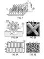
- FIG. 5A is a schematic diagram of one embodiment.
- FIG. 5B is a micrograph of a plurality of nanostructures of a type that may be employed in the embodiment shown in FIG. 5A .
- FIG. 6A is a schematic diagram of an embodiment employing nano-bowls.
- FIG. 6B is a micrograph of a plurality of nano-bowls of a type that may be employed in the embodiment shown in FIG. 6A .
- FIG. 7 is a schematic diagram of an embodiment that employs a reciprocating blade.
- FIG. 8A is a schematic diagram of a rotational embodiment.
- FIG. 8B is a micrograph of radially-disposed nanostructures of a type that may be employed in the embodiment shown in FIG. 8A .
- FIG. 9A is a schematic diagram of an embodiment employing two sets of nano-wires.
- FIG. 9B is a micrograph of a plurality of nano-wires of a type that may be employed in the embodiment shown in FIG. 9A .
- FIGS. 10A-10D are a series of schematic diagrams that demonstrate a method of making a sheet embodiment.
- FIG. 11 is a schematic diagram showing operation of an embodiment in response to acoustic wave energy.
- FIG. 12 is a top perspective view of a first patterned nanostructure embodiment.
- FIG. 13 is a top perspective view of a second patterned nanostructure embodiment.
- FIG. 14 is a top perspective view of a pyramidal conductive contact embodiment.
- a semiconductor piezoelectric structure 120 in one embodiment of a generator 100 , extends from a substrate 100 .
- the semiconductor piezoelectric structure 120 could include a nanostructure, such as a nano-wire, a nano-rod, a nano-belt or a nano-tube.
- One representative nanostructure could include a zinc oxide structure, as a zinc oxide crystal exhibits both the property of being piezoelectric and of acting as a semiconductor.
- a conductive contact 130 e.g., a probe tip of an atomic force microscope
- the semiconductor piezoelectric structure 120 bends, thereby creating a potential difference is created between a first side 126 (which is on the compressed side of the semiconductor piezoelectric structure 120 ) and a second side 128 (which is on the decompressed side).
- a reverse-biased Schottky barrier is formed between the conductive contact 130 and the second side 128 . Because the Schottky barrier is reverse-biased, no current flows between the conductive contact 130 and the semiconductor piezoelectric structure 120 .
- the Schottky barrier between the conductive contact 130 and the semiconductor piezoelectric structure 120 becomes forward-biased and current is allowed to flow through the Schottky barrier.
- Zinc oxide exhibits both semiconducting and piezoelectric properties.
- One embodiment of an electric generator employs aligned ZnO nano-wire arrays for converting nano-scale mechanical energy into electric energy.
- the operating mechanism of the electric generator relies on the coupling of piezoelectric and semiconducting dual properties of ZnO as well as the rectifying function of the Schottky barrier formed between the metal tip 130 and the nano-wire 120 .
- This approach has the potential of converting biological mechanical energy, acoustic or ultrasonic vibration energy, and biofluid hydraulic energy into electricity, which may result in self-powering of wireless nanodevices and nanosystems.
- NWs nano-wires
- NBs nano-belts
- wurtzite structured materials such as ZnO, GaN and ZnS
- One experimental embodiment employed mechanical manipulation of a single ZnO wire/belt 120 by a probe 130 coupled to an atomic force microscope (AFM).
- AFM atomic force microscope
- the measurements were performed by an AFM using a Silicon tip coated with Platinum film, which had a tetrahedral shape with an apex angle of 70°, was 14 ⁇ m in height, and had a spring constant of 1.42 N/m.
- the measurements were done in AFM contact mode under a constant normal force of 5 nN between the tip and the sample surface with a scan area of 70 ⁇ 70 ⁇ m 2 .
- Both the topography (feed back signal from the scanner) and the corresponding output voltage (V) images across a load were recorded simultaneously when the AFM tip was scanned across a wire or a belt.
- the topography image reflected the change in normal force perpendicular to the substrate, which showed a bump only when the tip scans over the wire.
- the output voltage between the conductive tip and the ground was continuously monitored as the tip scanned over the wire or the belt. No external voltage was applied in any stage of the experiment.
- the AFM tip 130 was scanned line-by-line at a speed of 105.57 ⁇ m/s perpendicular to the wire either from above the top end to the lower part of the wire or from the lower part towards the top end. For a wire with a hexagonal cross-section, three characteristic features were observed. When the tip scanned above the top end of the wire without touching the wire, the output voltage signal was nothing but noise. When the tip scanned until it touched the top end of the wire, a spark output voltage signal was observed. The output voltage is negative for the load R L , for almost all of the observed cases, indicating the tip has a lower potential than the grounded silver paste. When the tip 130 scanned down along the wire 120 , it deflected the wire but could not go over it, and the output voltage showed no peak but noise.
- ⁇ max is the maximum deflection angle at the top of the wire. Since:
- V ⁇ ⁇ TFL 2 4 ⁇ ⁇ d ⁇ ⁇ YI
- V ⁇ ⁇ 3 ⁇ ⁇ Ty m / 4 ⁇ ⁇ Ld
- the Pt metal-ZnO semiconductor (M-S) interface in this case is a reversely biased Schottky diode, resulting in little current flowing across the interface.
- the piezoelectric static charges mainly due to Zn 2+ and O 2 ⁇ ions, are accumulated and preserved, but without creating a current flow through the belt. This is a key process that prevents the slow “leakage” of the current as the deformation is being built up by the tip, otherwise, no observable output electric signal in the next step.
- the interface is thus a positively biased Schottky diode, and it is possible to have current flow from the tip through the belt 120 .
- the flow of electrons is to neutralize the piezoelectric ionic charges distributed in volume, resulting in a sudden increase in the output electric current.
- the output voltage measured on the load is negative in reference to the grounded root of the belt with consideration the flowing direction of the current.
- the elastic deformation energy as created by the displacement force F is mainly dissipated in three ways: creating mechanical resonance/vibration after releasing the belt 120 , generating piezoelectric discharge energy for each cycle of the vibration, and overcoming the friction and viscosity, if any, from the environmental and substrate.
- the mechanical resonance of the belt 120 may continue for many cycles, but it is eventually damped by the viscosity of the medium.
- the piezoelectric voltage output is generated in each cycle of the vibration, but the AFM tip 130 in the experimental design may be too slow to collect the electric signal output from each cycle of the belt vibration. It was found that the discharge signal can sometimes be collected for an extensive period of time, during which the belt may have resonated for over 10 cycles, producing a continuous and constant output DC voltage.
- the resonance frequency of the wire was about 10 KHz, and the scanning speed of the tip was about 10 ⁇ m/s, it is feasible that the wire 120 had contacted the AFM probe tip 130 over 100 times before it departed to the point that it was too far away to make contact. It was observed that a piezoelectric output voltage is created in each cycle of vibration. Thus a DC power source can be created by continuously collecting the output voltage.
- the energy was first created by the deflection force and stored by piezoelectric potential, and later converted into piezo-electric energy.
- the mechanism of the generator is the result of coupled semiconducting and piezoelectric properties of ZnO.
- the piezoelectric effect is required to create electric potential of ionic charges from elastic deformation; the semiconducting property is required to preserve the charges and then release the potential via the rectifying behavior of the Schottky barrier at the metal-ZnO interface, which serves as a switch in the entire process.
- the good conductivity of ZnO makes current flow possible. This process may also be possible for wurtzite structured materials such as GaN and ZnS.
- FIGS. 2A and 2B A second embodiment of a generator is shown in FIGS. 2A and 2B , in which a first conductive contact 210 is disposed at the first end 122 and a second conductive contact 212 is disposed at the second end 124 .
- the second conductive contact 212 could be either placed against the semiconductor piezoelectric structure 120 or placed against the substrate 110 if the substrate 110 is made of a conductive material.
- a load 214 is coupled between the first conductive contact 210 and the second conductive contact 212 so that when a force is applied to the first end 122 in direction F, a current I flows through the load 214 .
- FIGS. 3A-3D A third embodiment is shown in FIGS. 3A-3D .
- the first conductive contact 310 has an uneven surface.
- part of the semiconductor piezoelectric structure 120 makes contact with the first conductive contact 310 .
- This causes the semiconductor piezoelectric structure 120 to bend and a potential difference forms between the two sides of the semiconductor piezoelectric structure 120 .
- FIG. 3C only the positive side of the semiconductor piezoelectric structure 120 is in contact with the first conductive contact 310 , which creates a reverse-biased Schottky barrier through which no current flows.
- the negative side of the semiconductor piezoelectric structure 120 makes contact with the first conductive contact 310 , thereby forming a forward-biased Schottky barrier and allowing current to flow through the load 214 .
- the fact that the positive side of the semiconductor piezoelectric structure 120 may still be touching the first conductive contact 310 makes no difference since the Schottky barrier between the positive side and the first conductive contact 310 is still reverse-biased and, therefore, no current will flow through the positive side.
- the device in the forward-biased state has an energy band gap diagram 402 as shown in FIG. 4A , in which the conduction energy level (E c ) of the compressed side of the semiconductor piezoelectric structure (which is ZnO in the example presented) is greater than the Fermi energy (E f ) of the metal.
- E c conduction energy level
- E f Fermi energy
- the conduction energy level (E c ) of the compressed side is not greater than the Fermi energy (E f ) of the metal and, since the stretched side has a positive potential relative to the potential of the metal, current is not allowed to flow across the Schottky barrier 406 .
- FIG. 5A employs an array 520 of zinc oxide (ZnO) nanostructures 522 with a corrugated conductor 510 placed above the nanostructures 522 .
- a load 214 is coupled to the base of the nanostructure array 520 (forming an Ohmic contact therebetween) and to the corrugated conductor 510 .
- a micrograph of suitable ZnO nanostructures 522 is shown in FIG. 5B .
- a sheet 610 defining a plurality of nano-bowls 612 is used as the conductive contact.
- a micrograph of a plurality of nano-bowls 612 is shown in FIG. 6A .
- Suitable nano-bowls may be fabricated according to a method disclosed in detail in U.S. Patent Application Publication No. US-2005-0224779-A1 (Ser. No. 11/010,178, filed on Dec. 10, 2004), the entirety of which is incorporated by reference herein.
- This embodiment could be employed in generating electricity from body movement.
- this embodiment could be applied to the soles of a pair of shoes to generated electricity while the person wearing the shoes walks.
- FIG. 7 An embodiment that employs an array of nano-wires 520 that are activated by a reciprocating contact 710 is shown in FIG. 7 .
- the reciprocating contact 710 includes a metal contact blade 712 that is driven by an actuator 714 , such as a piston-type actuator.
- FIG. 8A A rotating generator is shown in FIG. 8A , in which a semiconductor piezoelectric structure 820 includes a plurality of nanorods 822 extending radially from a core 824 and that is capable of rotating about an axis in rotational direction R.
- the conductive contact 810 defines an opening 812 that is disposed so that as the nanorods 822 are drawn against edges of the contact 810 as the semiconductor piezoelectric structure 820 rotates.
- flowing fluid can cause the semiconductor piezoelectric structure 820 to rotate much in the way that a windmill rotates.
- This embodiment could be used as a generator within fluid flow structures, such as a blood vessel or a water pipe.
- FIG. 9A An embodiment for converting vibrational energy into electrical energy is shown in FIG. 9A , in which an array 920 of semiconductor piezoelectric nanostructures 922 is placed in an opposing relationship to an array 910 of conductive nanorods 912 .
- a first end 924 of at least some of the semiconductor piezoelectric nanorods 922 is adjacent to a first end 914 of at least some of a set of the conductive nanorods so that as the conductive nanorods 912 vibrate laterally (in directions V and V′) with respect to the semiconductor piezoelectric nanorods 922 , a forward-biased Schottky barrier is formed by contact of at least one of the conductive nanorods 912 and at least one of the semiconductor piezoelectric nanorods 922 , thereby generating an electrical current.
- FIG. 9B A micrograph of an array 920 of semiconductor piezoelectric nanorods 922 is shown in FIG. 9B .
- a plurality of catalyst particles 1022 (such as gold particles) is placed on a substrate 1010 .
- Zinc oxide nano-wires 120 are then grown from the catalyst particles 1022 using a process of the type disclosed in U.S. Patent Application Publication No. US-2005-0224779-A1.
- a deformable layer 1030 such as a layer of an organic polymer, is deposited onto the substrate 1010 to a level so that the deformable layer 1030 surrounds each of the plurality of zinc oxide semiconductor piezoelectric structures 120 to a predetermined level.
- An uneven conductive contact layer 1040 is placed above the nano-wires 120 so that as a downward force (in the direction of the arrows) is applied to the conductive contact layer 1040 , forward-biased Schottky barriers are formed (in the manner discussed with reference to FIGS. 3A-3D ) and a current is applied to the load 1032 .
- the deformable layer 1030 maintains the attitude of the nano-wires 120 , keeps them separated and prevents them from peeling off of the substrate 1010 .
- This embodiment may be subjected to extremely large deformation, so that they can be used for flexible electronics as a flexible or foldable power source.
- One reason for choosing zinc oxide in this embodiment is that it is a biocompatible and bio-safe material and, thus, it has a potential for being implanted as a power source in the human body.
- the flexibility of the polymer substrate used for growing zinc oxide nano-wires makes it feasible to accommodate the flexibility of human muscles so that it can use mechanical energy (body movement, muscle stretching) in the human body to generate electricity.
- FIGS. 10A-10D may also respond to acoustic wave or ultrasonic wave energy, as shown in FIG. 11 .
- Resonance of the nano-wires 120 as a one-end free beam can also generate electricity.
- the principles and technology demonstrated here have the potential of converting mechanical movement energy (such as body movement, muscle stretching, blood pressure), vibration energy (such as acoustic/ultrasonic wave), and hydraulic energy (such as flow of body fluid, blood flow, contraction of blood vessel, dynamic fluid in nature) into electric energy that may be sufficient for self-powering nanodevices and nanosystems.
- the technology could have important applications in wireless self-powered nanodevices by harvesting energy from the environment. It may also provide a method for indirectly charging of a battery.
- nano-generator could be the basis for using self-powering technology for in-situ, real-time and implantable biosensing, biomedical monitoring and biodetection. It could have the potential of solving key energy requirement for remote sensing and actuating.
- the nanostructures could be patterned in clusters 1220 or, as shown in FIG. 13 , individual nanostructures 1320 arranged in a pattern.
- the conductive contact could include an array of conductive pyramids 1440 .
Landscapes
- Engineering & Computer Science (AREA)
- Manufacturing & Machinery (AREA)
- General Electrical Machinery Utilizing Piezoelectricity, Electrostriction Or Magnetostriction (AREA)
- Electrodes Of Semiconductors (AREA)
Priority Applications (6)
| Application Number | Priority Date | Filing Date | Title |
|---|---|---|---|
| US11/608,865 US8330154B2 (en) | 2005-12-20 | 2006-12-11 | Piezoelectric and semiconducting coupled nanogenerators |
| EP06846573A EP1964161A4 (de) | 2005-12-20 | 2006-12-12 | Piezoelektrische und halbleitende gekoppelte nanogeneratoren |
| PCT/US2006/061933 WO2007076254A2 (en) | 2005-12-20 | 2006-12-12 | Piezoelectric and semiconducting coupled nanogenerators |
| JP2008547684A JP5026436B2 (ja) | 2005-12-20 | 2006-12-12 | 結合型の圧電半導体ナノ発電機 |
| US11/760,002 US8039834B2 (en) | 2006-06-13 | 2007-06-08 | Nanogenerator comprising piezoelectric semiconducting nanostructures and Schottky conductive contacts |
| US12/338,131 US8003982B2 (en) | 2005-12-20 | 2008-12-18 | Stacked mechanical nanogenerator comprising piezoelectric semiconducting nanostructures and Schottky conductive contacts |
Applications Claiming Priority (5)
| Application Number | Priority Date | Filing Date | Title |
|---|---|---|---|
| US75255805P | 2005-12-20 | 2005-12-20 | |
| US75963706P | 2006-01-18 | 2006-01-18 | |
| US79573406P | 2006-04-28 | 2006-04-28 | |
| US79644206P | 2006-05-01 | 2006-05-01 | |
| US11/608,865 US8330154B2 (en) | 2005-12-20 | 2006-12-11 | Piezoelectric and semiconducting coupled nanogenerators |
Related Child Applications (2)
| Application Number | Title | Priority Date | Filing Date |
|---|---|---|---|
| US11/760,002 Continuation-In-Part US8039834B2 (en) | 2006-06-13 | 2007-06-08 | Nanogenerator comprising piezoelectric semiconducting nanostructures and Schottky conductive contacts |
| US12/338,131 Continuation-In-Part US8003982B2 (en) | 2005-12-20 | 2008-12-18 | Stacked mechanical nanogenerator comprising piezoelectric semiconducting nanostructures and Schottky conductive contacts |
Publications (2)
| Publication Number | Publication Date |
|---|---|
| US20100117488A1 US20100117488A1 (en) | 2010-05-13 |
| US8330154B2 true US8330154B2 (en) | 2012-12-11 |
Family
ID=38218760
Family Applications (1)
| Application Number | Title | Priority Date | Filing Date |
|---|---|---|---|
| US11/608,865 Expired - Fee Related US8330154B2 (en) | 2005-12-20 | 2006-12-11 | Piezoelectric and semiconducting coupled nanogenerators |
Country Status (4)
| Country | Link |
|---|---|
| US (1) | US8330154B2 (de) |
| EP (1) | EP1964161A4 (de) |
| JP (1) | JP5026436B2 (de) |
| WO (1) | WO2007076254A2 (de) |
Cited By (4)
| Publication number | Priority date | Publication date | Assignee | Title |
|---|---|---|---|---|
| US20140313141A1 (en) * | 2013-04-23 | 2014-10-23 | Samsung Electronics Co., Ltd. | Smart apparatus having touch input module and energy generating device, and operating method of the smart apparatus |
| US9312468B2 (en) | 2012-02-23 | 2016-04-12 | Samsung Electronics Co., Ltd. | Nano-piezoelectric generator and method of manufacturing the same |
| US20170363486A1 (en) * | 2014-12-10 | 2017-12-21 | Paul D OKULOV | Micro electro-mechanical strain displacement sensor and usage monitoring system |
| US11594574B2 (en) | 2018-02-16 | 2023-02-28 | International Business Machines Corporation | Piezo-junction device |
Families Citing this family (53)
| Publication number | Priority date | Publication date | Assignee | Title |
|---|---|---|---|---|
| US7557433B2 (en) | 2004-10-25 | 2009-07-07 | Mccain Joseph H | Microelectronic device with integrated energy source |
| US20100312129A1 (en) | 2005-01-26 | 2010-12-09 | Schecter Stuart O | Cardiovascular haptic handle system |
| CN101587223A (zh) * | 2008-05-21 | 2009-11-25 | 鸿富锦精密工业(深圳)有限公司 | 氧化锌纳米线驱动器及采用其的镜头模组、相机模组 |
| KR101524766B1 (ko) * | 2008-08-07 | 2015-06-02 | 삼성전자주식회사 | 전기 에너지 발생 장치 및 그 제조 방법 |
| US7936111B2 (en) * | 2008-08-07 | 2011-05-03 | Samsung Electronics Co., Ltd. | Apparatus for generating electrical energy and method for manufacturing the same |
| US8278800B2 (en) * | 2008-08-21 | 2012-10-02 | Innowattech Ltd. | Multi-layer piezoelectric generator |
| US8758217B2 (en) * | 2008-09-02 | 2014-06-24 | Georgia Tech Research Corporation | Piezoelectric nanowire vibration sensors |
| KR101454686B1 (ko) * | 2008-09-17 | 2014-10-28 | 삼성전자주식회사 | 에너지 변환 장치 및 방법 |
| US9059397B2 (en) | 2008-12-08 | 2015-06-16 | Electronics And Telecommunications Research Institute | Nano piezoelectric device having a nanowire and method of forming the same |
| JP4971393B2 (ja) * | 2008-12-08 | 2012-07-11 | 韓國電子通信研究院 | ナノ圧電素子及びその形成方法 |
| US8354776B2 (en) * | 2008-12-22 | 2013-01-15 | Samsung Electronics Co., Ltd. | Apparatus for generating electrical energy and method for manufacturing the same |
| EP2410649B1 (de) * | 2009-03-18 | 2017-05-17 | Fujitsu Limited | Piezoelektrische stromerzeugungseinrichtung |
| KR101562060B1 (ko) | 2009-04-06 | 2015-10-21 | 삼성전자주식회사 | 전기 에너지 발생 장치 및 그 제조 방법 |
| US20100317978A1 (en) * | 2009-06-10 | 2010-12-16 | Maile Keith R | Implantable medical device housing modified for piezoelectric energy harvesting |
| US8283840B2 (en) * | 2009-06-15 | 2012-10-09 | Farrokh Mohamadi | High-efficiency compact miniaturized energy harvesting and storage device |
| KR100989410B1 (ko) * | 2009-10-06 | 2010-10-25 | 전남대학교산학협력단 | 전기활성 고분자 변환기 및 이를 이용한 에너지 포집장치 |
| US8415859B2 (en) * | 2009-10-27 | 2013-04-09 | Korea University Research And Business Foundation | Piezoelectric nanodevices |
| US8623451B2 (en) * | 2009-11-10 | 2014-01-07 | Georgia Tech Research Corporation | Large-scale lateral nanowire arrays nanogenerators |
| US8558329B2 (en) | 2009-11-13 | 2013-10-15 | Georgia Tech Research Corporation | Piezo-phototronic sensor |
| KR101588318B1 (ko) * | 2009-11-23 | 2016-01-25 | 삼성전자주식회사 | 튜브형 압전 에너지 발생 장치 및 그 제조방법 |
| US8367462B2 (en) | 2010-04-21 | 2013-02-05 | Georgia Tech Research Corporation | Large-scale fabrication of vertically aligned ZnO nanowire arrays |
| KR101205346B1 (ko) * | 2010-07-21 | 2012-11-28 | 삼성중공업 주식회사 | 슬로싱 현상을 이용하는 나노발전기를 구비한 선박 |
| JP5353865B2 (ja) * | 2010-11-19 | 2013-11-27 | 株式会社豊田中央研究所 | 発電装置及び発電方法 |
| US8865574B2 (en) * | 2010-11-30 | 2014-10-21 | Michael Haag | Method for deposition of nanoparticles onto substrates |
| US8680751B2 (en) | 2010-12-02 | 2014-03-25 | Georgia Tech Research Corporation | Hybrid nanogenerator for harvesting chemical and mechanical energy |
| US8518736B2 (en) | 2010-12-29 | 2013-08-27 | Georgia Tech Research Corporation | Growth and transfer of monolithic horizontal nanowire superstructures onto flexible substrates |
| KR101713280B1 (ko) * | 2011-03-03 | 2017-03-08 | 삼성전자주식회사 | 전기 에너지 발생장치 |
| US8942828B1 (en) | 2011-04-13 | 2015-01-27 | Stuart Schecter, LLC | Minimally invasive cardiovascular support system with true haptic coupling |
| WO2012158914A1 (en) | 2011-05-17 | 2012-11-22 | Georgia Tech Research Corporation | Nanogenerator for self-powered system with wireless data transmission |
| US9368710B2 (en) | 2011-05-17 | 2016-06-14 | Georgia Tech Research Corporation | Transparent flexible nanogenerator as self-powered sensor for transportation monitoring |
| KR101781551B1 (ko) * | 2011-07-20 | 2017-09-27 | 삼성전자주식회사 | 전기에너지 발생 소자 및 그 구동방법 |
| KR101769459B1 (ko) * | 2011-08-10 | 2017-08-21 | 삼성전자주식회사 | 나노 발전 소자 및 그 제조 방법 |
| WO2013040137A1 (en) | 2011-09-13 | 2013-03-21 | Georgia Tech Research Corporation | Self-charging power pack |
| KR101624430B1 (ko) * | 2011-10-28 | 2016-05-25 | 시안 지아오통 유니버시티 | 나노-압전 센서들의 어레이에 동작가능하게 커플링된 플렉서블 마이크로 범프들 |
| US8778731B2 (en) | 2011-11-03 | 2014-07-15 | Samsung Electronics Co., Ltd. | Method of manufacturing P-type ZnO nanowires and method of manufacturing energy conversion device |
| KR101313620B1 (ko) | 2011-11-03 | 2013-10-02 | 삼성중공업 주식회사 | 압전소자가 설치된 선박용 저장탱크 및 이를 포함하는 선박 |
| KR20130069035A (ko) * | 2011-12-16 | 2013-06-26 | 삼성전자주식회사 | 그래핀상의 하이브리드 나노구조체 형성 방법 |
| CN103356326B (zh) * | 2012-04-01 | 2016-08-03 | 创新神经科技有限公司 | 眼部植入装置及眼部植入装置升级系统 |
| US10013082B2 (en) | 2012-06-05 | 2018-07-03 | Stuart Schecter, LLC | Operating system with haptic interface for minimally invasive, hand-held surgical instrument |
| US9024395B2 (en) | 2012-09-07 | 2015-05-05 | Georgia Tech Research Corporation | Taxel-addressable matrix of vertical nanowire piezotronic transistors |
| US9455399B2 (en) | 2012-09-12 | 2016-09-27 | Georgia Tech Research Corporation | Growth of antimony doped P-type zinc oxide nanowires for optoelectronics |
| US9774277B2 (en) * | 2012-11-13 | 2017-09-26 | The Board Of Trustees Of The Leland Stanford Junior University | Energy harvesting |
| US9112432B2 (en) | 2012-12-14 | 2015-08-18 | Samsung Electronics Co., Ltd. | Piezoelectric generator and method of manufacturing the same |
| US20140174496A1 (en) | 2012-12-21 | 2014-06-26 | Georgia Tech Research Corporation | Hybrid generator using thermoelectric generation and piezoelectric generation |
| KR102051518B1 (ko) | 2013-01-28 | 2019-12-03 | 삼성전자주식회사 | 자가 동력 터치 센서 겸용 에너지 수확 장치 |
| US9147845B2 (en) | 2013-04-26 | 2015-09-29 | Samsung Electronics Co., Ltd. | Single walled carbon nanotube-based planar photodector |
| US9444031B2 (en) | 2013-06-28 | 2016-09-13 | Samsung Electronics Co., Ltd. | Energy harvester using mass and mobile device including the energy harvester |
| US9837933B2 (en) * | 2013-06-28 | 2017-12-05 | Samsung Electronics Co., Ltd. | Energy harvester using mass and mobile device including the energy harvester |
| JP6044586B2 (ja) * | 2014-05-15 | 2016-12-14 | 株式会社豊田中央研究所 | 発電装置及び発電方法 |
| US10526884B2 (en) | 2014-08-01 | 2020-01-07 | William Marsh Rice University | Systems and methods for monitoring cement quality in a cased well environment with integrated chips |
| US9660470B2 (en) * | 2014-09-08 | 2017-05-23 | Nokia Technologies Oy | Flexible, hybrid energy generating and storage power cell |
| EP4252833B1 (de) | 2015-11-17 | 2026-02-11 | Inspire Medical Systems, Inc. | Vorrichtung mit mikrostimulation zur therapie von schlafatmungsstörungen |
| CN116314046B (zh) * | 2023-05-18 | 2023-07-21 | 华中科技大学 | 一种传输特性可调的压电三极管模块及其调控方法和应用 |
Citations (20)
| Publication number | Priority date | Publication date | Assignee | Title |
|---|---|---|---|---|
| US3500451A (en) | 1967-06-29 | 1970-03-10 | Gen Telephone & Elect | Piezoelectric voltage generator |
| JPS5133373A (ja) | 1974-08-31 | 1976-03-22 | Mitsubishi Metal Corp | Setsusakukogunonagasachoseijigu |
| JPH09233861A (ja) | 1996-02-22 | 1997-09-05 | Seiko Epson Corp | 発電装置およびこれを備えた携帯型電子機器 |
| JP2003073859A (ja) | 2001-09-03 | 2003-03-12 | National Institute For Materials Science | 基体上に接合して規則化配列したナノ構造体およびその製造方法 |
| US6559550B2 (en) * | 2000-11-03 | 2003-05-06 | Lockheed Martin Corporation | Nanoscale piezoelectric generation system using carbon nanotube |
| US20030205657A1 (en) | 2002-05-01 | 2003-11-06 | Voisin Ronald D. | Methods of manufacturing a lithography template |
| US20040127025A1 (en) | 2002-08-26 | 2004-07-01 | Crocker Percy Vandorn | Processes for fabricating conductive patterns using nanolithography as a patterning tool |
| WO2005006346A2 (en) | 2003-07-08 | 2005-01-20 | Qunano Ab | Probe structures incorporating nanowhiskers, production methods thereof, and methods of forming nanowhiskers |
| US20050188751A1 (en) | 1997-06-16 | 2005-09-01 | Puskas William L. | Sensing system for measuring cavitation |
| JP2005237156A (ja) | 2004-02-23 | 2005-09-02 | Taiheiyo Cement Corp | 発電装置および発電システム |
| US20050242366A1 (en) | 2001-07-23 | 2005-11-03 | Cree, Inc. | Gallium nitride based diodes with low forward voltage and low reverse current operation |
| US20090309456A1 (en) * | 2008-03-17 | 2009-12-17 | Georgia Tech Research Corporation | Piezoelectric-Coated Carbon Nanotube Generators |
| US20100033059A1 (en) * | 2008-08-07 | 2010-02-11 | Samsung Electronics Co., Ltd. | Apparatus for generating electrical energy and method for manufacturing the same |
| US20100066208A1 (en) * | 2008-09-17 | 2010-03-18 | Samsung Electronics, Co., Ltd. | Apparatus and method for converting energy |
| US20100139750A1 (en) * | 2008-12-04 | 2010-06-10 | Electronics And Telecommunications Research Institute | Flexible energy conversion device and method of manufacturing the same |
| US20100141095A1 (en) * | 2008-12-08 | 2010-06-10 | Electronics And Telecommunications Research Institute | Nano piezoelectric device and method of forming the same |
| US20100253184A1 (en) * | 2009-04-06 | 2010-10-07 | Samsung Electronics Co., Ltd. | Apparatus for generating electrical energy and method for manufacturing the same |
| US7839028B2 (en) * | 2007-04-03 | 2010-11-23 | CJP IP Holding, Ltd. | Nanoelectromechanical systems and methods for making the same |
| US8003982B2 (en) * | 2005-12-20 | 2011-08-23 | Georgia Tech Research Corporation | Stacked mechanical nanogenerator comprising piezoelectric semiconducting nanostructures and Schottky conductive contacts |
| US8039834B2 (en) * | 2006-06-13 | 2011-10-18 | Georgia Tech Research Corporation | Nanogenerator comprising piezoelectric semiconducting nanostructures and Schottky conductive contacts |
Family Cites Families (5)
| Publication number | Priority date | Publication date | Assignee | Title |
|---|---|---|---|---|
| JPS5133373U (de) * | 1974-09-02 | 1976-03-11 | ||
| US5801475A (en) * | 1993-09-30 | 1998-09-01 | Mitsuteru Kimura | Piezo-electricity generation device |
| US7371962B2 (en) * | 1999-05-04 | 2008-05-13 | Neokismet, Llc | Diode energy converter for chemical kinetic electron energy transfer |
| US6996147B2 (en) * | 2001-03-30 | 2006-02-07 | The Regents Of The University Of California | Methods of fabricating nanostructures and nanowires and devices fabricated therefrom |
| US7351607B2 (en) | 2003-12-11 | 2008-04-01 | Georgia Tech Research Corporation | Large scale patterned growth of aligned one-dimensional nanostructures |
-
2006
- 2006-12-11 US US11/608,865 patent/US8330154B2/en not_active Expired - Fee Related
- 2006-12-12 JP JP2008547684A patent/JP5026436B2/ja not_active Expired - Fee Related
- 2006-12-12 WO PCT/US2006/061933 patent/WO2007076254A2/en not_active Ceased
- 2006-12-12 EP EP06846573A patent/EP1964161A4/de not_active Withdrawn
Patent Citations (20)
| Publication number | Priority date | Publication date | Assignee | Title |
|---|---|---|---|---|
| US3500451A (en) | 1967-06-29 | 1970-03-10 | Gen Telephone & Elect | Piezoelectric voltage generator |
| JPS5133373A (ja) | 1974-08-31 | 1976-03-22 | Mitsubishi Metal Corp | Setsusakukogunonagasachoseijigu |
| JPH09233861A (ja) | 1996-02-22 | 1997-09-05 | Seiko Epson Corp | 発電装置およびこれを備えた携帯型電子機器 |
| US20050188751A1 (en) | 1997-06-16 | 2005-09-01 | Puskas William L. | Sensing system for measuring cavitation |
| US6559550B2 (en) * | 2000-11-03 | 2003-05-06 | Lockheed Martin Corporation | Nanoscale piezoelectric generation system using carbon nanotube |
| US20050242366A1 (en) | 2001-07-23 | 2005-11-03 | Cree, Inc. | Gallium nitride based diodes with low forward voltage and low reverse current operation |
| JP2003073859A (ja) | 2001-09-03 | 2003-03-12 | National Institute For Materials Science | 基体上に接合して規則化配列したナノ構造体およびその製造方法 |
| US20030205657A1 (en) | 2002-05-01 | 2003-11-06 | Voisin Ronald D. | Methods of manufacturing a lithography template |
| US20040127025A1 (en) | 2002-08-26 | 2004-07-01 | Crocker Percy Vandorn | Processes for fabricating conductive patterns using nanolithography as a patterning tool |
| WO2005006346A2 (en) | 2003-07-08 | 2005-01-20 | Qunano Ab | Probe structures incorporating nanowhiskers, production methods thereof, and methods of forming nanowhiskers |
| JP2005237156A (ja) | 2004-02-23 | 2005-09-02 | Taiheiyo Cement Corp | 発電装置および発電システム |
| US8003982B2 (en) * | 2005-12-20 | 2011-08-23 | Georgia Tech Research Corporation | Stacked mechanical nanogenerator comprising piezoelectric semiconducting nanostructures and Schottky conductive contacts |
| US8039834B2 (en) * | 2006-06-13 | 2011-10-18 | Georgia Tech Research Corporation | Nanogenerator comprising piezoelectric semiconducting nanostructures and Schottky conductive contacts |
| US7839028B2 (en) * | 2007-04-03 | 2010-11-23 | CJP IP Holding, Ltd. | Nanoelectromechanical systems and methods for making the same |
| US20090309456A1 (en) * | 2008-03-17 | 2009-12-17 | Georgia Tech Research Corporation | Piezoelectric-Coated Carbon Nanotube Generators |
| US20100033059A1 (en) * | 2008-08-07 | 2010-02-11 | Samsung Electronics Co., Ltd. | Apparatus for generating electrical energy and method for manufacturing the same |
| US20100066208A1 (en) * | 2008-09-17 | 2010-03-18 | Samsung Electronics, Co., Ltd. | Apparatus and method for converting energy |
| US20100139750A1 (en) * | 2008-12-04 | 2010-06-10 | Electronics And Telecommunications Research Institute | Flexible energy conversion device and method of manufacturing the same |
| US20100141095A1 (en) * | 2008-12-08 | 2010-06-10 | Electronics And Telecommunications Research Institute | Nano piezoelectric device and method of forming the same |
| US20100253184A1 (en) * | 2009-04-06 | 2010-10-07 | Samsung Electronics Co., Ltd. | Apparatus for generating electrical energy and method for manufacturing the same |
Non-Patent Citations (8)
| Title |
|---|
| Gao et al., Nanoarchitectures of semiconducting and piezoelectric zinc oxide, J. Applied Physics 97, 044304 (2005). |
| Jeon et al., "MEMS power generator with transverse mode thin film PZT", Sensors and Actuators A: Physical, vol. 122, No. 1, p. 16-22, Jul. 29, 1005. * |
| Lao et al., "Formation of double-side teethed nanocombs of ZnO and self-calalysis of Zn-terminated polar surface," Chemical Physics Letters (Science Direct), (Abstract), 2007. |
| Lao et al., "Formation of double-side teethed nanocombs of ZnO and self-catalysis of Zn-terminated polar surface," Chemical Physics Letters, Elsevier B.V., 2005. |
| Peck-Radosavjevic et al., "Thrombopoietin induces rapid resolution of thrombocytopenia after orthotopic liver transplantation through increased platelet production," Blood, vol. 95, No. 3, (2000). |
| Wang et al., "Large-Size Liftable Inverted-Nanobowl Sheets as REusable Masks for Nanolithography," Nano Letters, vol. 5, (Abstract), 2005. |
| Wang et al., "Large-Size Liftable Inverted-Nanobowl Sheets as Reusable Masks for Nanolithography," Nano Letters, vol. 5, No. 9, 2005, 1748-1788. |
| Wang et al., "Piezoelectric Nanogenerators Based on Zinc Oxide Nanowire Arrays," Science, vol. 312, pp. 242-245, Apr. 14, 2006. |
Cited By (6)
| Publication number | Priority date | Publication date | Assignee | Title |
|---|---|---|---|---|
| US9312468B2 (en) | 2012-02-23 | 2016-04-12 | Samsung Electronics Co., Ltd. | Nano-piezoelectric generator and method of manufacturing the same |
| US20140313141A1 (en) * | 2013-04-23 | 2014-10-23 | Samsung Electronics Co., Ltd. | Smart apparatus having touch input module and energy generating device, and operating method of the smart apparatus |
| US20170363486A1 (en) * | 2014-12-10 | 2017-12-21 | Paul D OKULOV | Micro electro-mechanical strain displacement sensor and usage monitoring system |
| US10663357B2 (en) * | 2014-12-10 | 2020-05-26 | Paul D OKULOV | Micro electro-mechanical strain displacement sensor and usage monitoring system |
| US11714012B2 (en) | 2014-12-10 | 2023-08-01 | Ipr Innovative Products Resources, Inc. | Micro electro-mechanical strain displacement sensor and system for monitoring health and usage of a structure |
| US11594574B2 (en) | 2018-02-16 | 2023-02-28 | International Business Machines Corporation | Piezo-junction device |
Also Published As
| Publication number | Publication date |
|---|---|
| JP2009521203A (ja) | 2009-05-28 |
| WO2007076254A2 (en) | 2007-07-05 |
| EP1964161A2 (de) | 2008-09-03 |
| EP1964161A4 (de) | 2011-03-09 |
| US20100117488A1 (en) | 2010-05-13 |
| WO2007076254A3 (en) | 2008-04-03 |
| JP5026436B2 (ja) | 2012-09-12 |
Similar Documents
| Publication | Publication Date | Title |
|---|---|---|
| US20100117488A1 (en) | Piezoelectric and semiconducting coupled nanogenerators | |
| US8003982B2 (en) | Stacked mechanical nanogenerator comprising piezoelectric semiconducting nanostructures and Schottky conductive contacts | |
| US8039834B2 (en) | Nanogenerator comprising piezoelectric semiconducting nanostructures and Schottky conductive contacts | |
| Wang et al. | Piezoelectric nanogenerators for self-powered nanodevices | |
| US8623451B2 (en) | Large-scale lateral nanowire arrays nanogenerators | |
| Wang | Piezoelectric nanogenerators—Harvesting ambient mechanical energy at the nanometer scale | |
| Li et al. | Recent progress on piezoelectric energy harvesting: structures and materials | |
| Gao et al. | Nanowire piezoelectric nanogenerators on plastic substrates as flexible power sources for nanodevices | |
| US9419544B2 (en) | Energy harvesting device having self-powered touch sensor | |
| Wang | The new field of nanopiezotronics | |
| Wang | Towards self‐powered nanosystems: from nanogenerators to nanopiezotronics | |
| Saravanakumar et al. | Fabrication of a ZnO nanogenerator for eco-friendly biomechanical energy harvesting | |
| US12301139B2 (en) | 1D/2D hybrid piezoelectric nanogenerator and method for making same | |
| KR101861148B1 (ko) | 나노 압전 발전 소자 및 그 제조방법 | |
| US20090309456A1 (en) | Piezoelectric-Coated Carbon Nanotube Generators | |
| EP2615656B1 (de) | Nanopiezoelektrischer Generator und Herstellungsverfahren dafür | |
| Sharov et al. | InP/Si heterostructure for high-current hybrid triboelectric/photovoltaic generation | |
| CN107799649B (zh) | 压电能量收集器件及其制造方法 | |
| Chen et al. | Anisotropic outputs of a nanogenerator from oblique-aligned ZnO nanowire arrays | |
| KR20190072086A (ko) | 스프링을 포함하는 마찰전기 발전 소자 | |
| Wang | Nanogenerators and nanopiezotronics | |
| Kong et al. | Waste mechanical energy harvesting (II): nanopiezoelectric effect | |
| KR20130063365A (ko) | 에너지 수확 소자 및 이를 제조하는 방법 | |
| Wang et al. | Mechanical Energy Harvesting Using Wurtzite Nanowires | |
| Wang et al. | for Self-Powered Nanodevices |
Legal Events
| Date | Code | Title | Description |
|---|---|---|---|
| AS | Assignment |
Owner name: GEORGIA TECH RESEARCH CORPORATION,GEORGIA Free format text: ASSIGNMENT OF ASSIGNORS INTEREST;ASSIGNORS:WANG, ZHONG L.;SONG, JINHUI;WANG, XUDONG;REEL/FRAME:018646/0698 Effective date: 20061211 Owner name: GEORGIA TECH RESEARCH CORPORATION, GEORGIA Free format text: ASSIGNMENT OF ASSIGNORS INTEREST;ASSIGNORS:WANG, ZHONG L.;SONG, JINHUI;WANG, XUDONG;REEL/FRAME:018646/0698 Effective date: 20061211 |
|
| AS | Assignment |
Owner name: NATIONAL SCIENCE FOUNDATION,VIRGINIA Free format text: EXECUTIVE ORDER 9424, CONFIRMATORY LICENSE;ASSIGNOR:TECHNOLOGY, GEORGIA INSTITUTE OF;REEL/FRAME:021734/0731 Effective date: 20080908 Owner name: NATIONAL SCIENCE FOUNDATION, VIRGINIA Free format text: EXECUTIVE ORDER 9424, CONFIRMATORY LICENSE;ASSIGNOR:TECHNOLOGY, GEORGIA INSTITUTE OF;REEL/FRAME:021734/0731 Effective date: 20080908 |
|
| AS | Assignment |
Owner name: NASA,DISTRICT OF COLUMBIA Free format text: CONFIRMATORY LICENSE;ASSIGNOR:GEORGIA TECH RESEARCH CORPORATION;REEL/FRAME:021959/0547 Effective date: 20080808 Owner name: NASA, DISTRICT OF COLUMBIA Free format text: CONFIRMATORY LICENSE;ASSIGNOR:GEORGIA TECH RESEARCH CORPORATION;REEL/FRAME:021959/0547 Effective date: 20080808 |
|
| STCF | Information on status: patent grant |
Free format text: PATENTED CASE |
|
| FPAY | Fee payment |
Year of fee payment: 4 |
|
| FEPP | Fee payment procedure |
Free format text: MAINTENANCE FEE REMINDER MAILED (ORIGINAL EVENT CODE: REM.); ENTITY STATUS OF PATENT OWNER: SMALL ENTITY |
|
| LAPS | Lapse for failure to pay maintenance fees |
Free format text: PATENT EXPIRED FOR FAILURE TO PAY MAINTENANCE FEES (ORIGINAL EVENT CODE: EXP.); ENTITY STATUS OF PATENT OWNER: SMALL ENTITY |
|
| STCH | Information on status: patent discontinuation |
Free format text: PATENT EXPIRED DUE TO NONPAYMENT OF MAINTENANCE FEES UNDER 37 CFR 1.362 |
|
| FP | Lapsed due to failure to pay maintenance fee |
Effective date: 20201211 |