US8247305B2 - Method and resulting structure for deep trench polysilicon hard mask removal - Google Patents
Method and resulting structure for deep trench polysilicon hard mask removal Download PDFInfo
- Publication number
- US8247305B2 US8247305B2 US12/960,357 US96035710A US8247305B2 US 8247305 B2 US8247305 B2 US 8247305B2 US 96035710 A US96035710 A US 96035710A US 8247305 B2 US8247305 B2 US 8247305B2
- Authority
- US
- United States
- Prior art keywords
- forming
- semiconductor substrate
- layer
- oxide layer
- etching process
- Prior art date
- Legal status (The legal status is an assumption and is not a legal conclusion. Google has not performed a legal analysis and makes no representation as to the accuracy of the status listed.)
- Active
Links
Images


Classifications
-
- H—ELECTRICITY
- H10—SEMICONDUCTOR DEVICES; ELECTRIC SOLID-STATE DEVICES NOT OTHERWISE PROVIDED FOR
- H10D—INORGANIC ELECTRIC SEMICONDUCTOR DEVICES
- H10D1/00—Resistors, capacitors or inductors
- H10D1/01—Manufacture or treatment
- H10D1/041—Manufacture or treatment of capacitors having no potential barriers
- H10D1/042—Manufacture or treatment of capacitors having no potential barriers using deposition processes to form electrode extensions
-
- H—ELECTRICITY
- H10—SEMICONDUCTOR DEVICES; ELECTRIC SOLID-STATE DEVICES NOT OTHERWISE PROVIDED FOR
- H10D—INORGANIC ELECTRIC SEMICONDUCTOR DEVICES
- H10D1/00—Resistors, capacitors or inductors
- H10D1/01—Manufacture or treatment
- H10D1/045—Manufacture or treatment of capacitors having potential barriers, e.g. varactors
- H10D1/047—Manufacture or treatment of capacitors having potential barriers, e.g. varactors of conductor-insulator-semiconductor capacitors, e.g. trench capacitors
-
- H—ELECTRICITY
- H10—SEMICONDUCTOR DEVICES; ELECTRIC SOLID-STATE DEVICES NOT OTHERWISE PROVIDED FOR
- H10D—INORGANIC ELECTRIC SEMICONDUCTOR DEVICES
- H10D1/00—Resistors, capacitors or inductors
- H10D1/60—Capacitors
- H10D1/62—Capacitors having potential barriers
- H10D1/66—Conductor-insulator-semiconductor capacitors, e.g. MOS capacitors
- H10D1/665—Trench conductor-insulator-semiconductor capacitors, e.g. trench MOS capacitors
-
- H—ELECTRICITY
- H10—SEMICONDUCTOR DEVICES; ELECTRIC SOLID-STATE DEVICES NOT OTHERWISE PROVIDED FOR
- H10D—INORGANIC ELECTRIC SEMICONDUCTOR DEVICES
- H10D1/00—Resistors, capacitors or inductors
- H10D1/60—Capacitors
- H10D1/68—Capacitors having no potential barriers
- H10D1/692—Electrodes
- H10D1/711—Electrodes having non-planar surfaces, e.g. formed by texturisation
- H10D1/716—Electrodes having non-planar surfaces, e.g. formed by texturisation having vertical extensions
-
- H—ELECTRICITY
- H10—SEMICONDUCTOR DEVICES; ELECTRIC SOLID-STATE DEVICES NOT OTHERWISE PROVIDED FOR
- H10P—GENERIC PROCESSES OR APPARATUS FOR THE MANUFACTURE OR TREATMENT OF DEVICES COVERED BY CLASS H10
- H10P50/00—Etching of wafers, substrates or parts of devices
- H10P50/69—Etching of wafers, substrates or parts of devices using masks for semiconductor materials
- H10P50/691—Etching of wafers, substrates or parts of devices using masks for semiconductor materials for Group V materials or Group III-V materials
- H10P50/692—Etching of wafers, substrates or parts of devices using masks for semiconductor materials for Group V materials or Group III-V materials characterised by their composition, e.g. multilayer masks or materials
-
- H—ELECTRICITY
- H10—SEMICONDUCTOR DEVICES; ELECTRIC SOLID-STATE DEVICES NOT OTHERWISE PROVIDED FOR
- H10P—GENERIC PROCESSES OR APPARATUS FOR THE MANUFACTURE OR TREATMENT OF DEVICES COVERED BY CLASS H10
- H10P50/00—Etching of wafers, substrates or parts of devices
- H10P50/69—Etching of wafers, substrates or parts of devices using masks for semiconductor materials
- H10P50/691—Etching of wafers, substrates or parts of devices using masks for semiconductor materials for Group V materials or Group III-V materials
- H10P50/693—Etching of wafers, substrates or parts of devices using masks for semiconductor materials for Group V materials or Group III-V materials characterised by their size, orientation, disposition, behaviour or shape, in horizontal or vertical plane
- H10P50/695—Etching of wafers, substrates or parts of devices using masks for semiconductor materials for Group V materials or Group III-V materials characterised by their size, orientation, disposition, behaviour or shape, in horizontal or vertical plane characterised by the process involved to create the mask, e.g. lift-off masks or sidewalls or to modify the mask
Definitions
- Embodiments of the present invention are directed to integrated circuits and their processing for the manufacture of semiconductor devices. More particularly, embodiments of the invention provide a method and structures for manufacturing a capacitor structure for dynamic random access memory devices, commonly called DRAMs. But it would be recognized that the invention has a much broader range of applicability.
- Integrated circuits have evolved from a handful of interconnected devices fabricated on a single chip of silicon to millions of devices.
- Conventional integrated circuits provide performance and complexity far beyond what was originally imagined.
- the size of the smallest device feature also known as the device “geometry”, has become smaller with each generation of integrated circuits.
- capacitor structures for memory devices.
- Such capacitor structures include, among others, trench designs, stack designs, and others. Although there have been significant improvements, such designs still have many limitations. As merely an example, these designs must become smaller and smaller but still provide high capacitance values and low leakage characteristics. Additionally, these capacitor designs are often difficult to manufacture and generally require complex manufacturing processes and structures.
- embodiments of the present invention techniques for processing integrated circuits for the manufacture of semiconductor devices are provided. More particularly, embodiments of the present invention provide a method and structures for manufacturing a capacitor structure for dynamic random access memory devices, commonly called DRAMs. But it would be recognized that the invention has a much broader range of applicability.
- a specific embodiment of the present invention provides a method of forming a capacitor structure for a dynamic random access memory integrated circuit.
- the method includes providing a semiconductor substrate, e.g., silicon wafer.
- the method includes forming a pad oxide layer (e.g., silicon oxide) overlying the semiconductor substrate.
- the method includes forming a nitride layer overlying the pad oxide layer and forming an interlayer dielectric layer overlying the nitride layer.
- the method includes forming a polysilicon mask layer overlying the interlayer dielectric layer and patterning the polysilicon mask layer to form an opening therein for a trench structure.
- the method includes applying a first reactive ion etching process to form a first trench region through a portion of the interlayer dielectric layer using the patterned polysilicon mask layer and maintaining the first reactive ion etching process to etch through a portion of the nitride layer and through a portion of the pad oxide layer.
- the method includes ceasing the first reactive ion etching process when a surface region of the semiconductor substrate has been exposed.
- the method also includes forming an oxide layer overlying at least the exposed surface region of the semiconductor substrate to protect the exposed surface region of the semiconductor substrate and removing the patterned polysilicon mask material while protecting the surface region of the semiconductor substrate using the oxide layer.
- the method applies a second reactive ion etching process to continue to form a second trench region by removing the oxide layer and removing a portion of the semiconductor substrate to a predetermined depth in the semiconductor substrate, wherein the second trench region is an extension of the first trench region into the semiconductor substrate.
- An alternative specific embodiment of the present invention provides a method of forming a capacitor structure for a dynamic random access memory integrated circuit.
- the method includes providing a semiconductor substrate, e.g., silicon wafer.
- the method includes forming a pad layer (e.g., silicon oxide) overlying the semiconductor substrate.
- the method includes forming a nitride layer overlying the pad layer and forming an interlayer dielectric layer overlying the nitride layer.
- the method includes forming a polysilicon mask layer overlying the interlayer dielectric layer and patterning the polysilicon mask layer to form an opening therein for a trench structure.
- the method includes applying a first reactive ion etching process to form a trench region through a portion of the interlayer dielectric layer while using the patterned polysilicon mask layer and maintaining the reactive ion etching process to etch through a portion of the nitride layer and through a portion of the pad oxide layer.
- the method includes ceasing the reactive ion etching process when a surface region of the semiconductor substrate has been exposed.
- the method includes forming an oxide layer overlying at least the exposed surface region of the semiconductor substrate to protect the surface region of the substrate.
- the oxide layer is less than 50 Angstroms or less than 30 Angstroms.
- the method includes removing the patterned polysilicon mask material while protecting the surface region of the semiconductor substrate using the oxide layer.
- the method applies a second reactive ion etching process to continue to form the trench region by removing the oxide layer and removing a portion of the semiconductor substrate to a predetermined depth in the semiconductor substrate.
- the method further includes forming a lower electrode plate overlying the trench region, forming a dielectric layer overlying the lower electrode plate, and forming an upper electrode plate overlying the dielectric layer to complete the capacitor structure.
- Embodiments of the present invention provide many benefits over conventional techniques.
- the present technique provides an easy to use process that relies upon conventional technology.
- Embodiments of the present invention provide higher device yields in dies per wafer.
- the embodiments of the present invention provide a process that is compatible with conventional process technology without substantial modifications to conventional equipment and processes.
- the invention provides for improved process integration for design rules of 0.13 microns and less.
- embodiments of the invention provide capacitor structures having improved characteristics. Depending upon the embodiment, one or more of these benefits may be achieved.
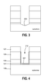
- FIGS. 1 through 6 are simplified cross-sectional view diagrams illustrating a method for forming a capacitor structure according to an embodiment of the present invention.
- Embodiments of the present invention provide techniques of processing integrated circuits for the manufacture of semiconductor devices. More particularly, embodiments of the invention provides a method and structures for manufacturing a capacitor structure for dynamic random access memory devices, commonly called DRAMs. Merely by way of example, embodiments of the invention have been applied to the formation of a capacitor structure for a dynamic random access memory device, but it would be recognized that the invention has a much broader range of applicability.
- a semiconductor substrate e.g., silicon wafer
- the above sequence of steps provides a method according to an embodiment of the present invention. As shown, the method uses a combination of steps including a way of forming a capacitor structure for a dynamic random access memory device. Other alternatives can also be provided where steps are added, one or more steps are removed, or one or more steps are provided in a different sequence without departing from the scope of the claims herein. Further details of the invention can be found throughout the present specification and more particularly below.
- FIGS. 1 through 6 are simplified cross-sectional view diagrams illustrating a method of forming a capacitor structure according to an embodiment of the present invention. These diagrams are merely examples, which should not unduly limit the scope of the claims herein. One of ordinary skill in the art would recognize many variations, alternatives, and modifications.
- the method includes providing a semiconductor substrate 100 , e.g., silicon wafer, silicon on insulator (step 1 ).
- the method includes forming a pad oxide layer 101 (e.g., silicon oxide, silicon oxide nitride) overlying the semiconductor substrate (step 2 ).
- the method includes forming a nitride layer 103 overlying the pad oxide layer (step 3 ).
- the nitride layer is silicon nitride or other suitable material.
- the method includes forming an interlayer dielectric layer 105 overlying the nitride layer (step 4 ).
- the interlayer dielectric material can be a suitable material such as PSG (phosphosilicate glass), BPSG (borophosphosilicate glass), FSG (fluorinated silicon glass), or the like.
- the method includes forming a polysilicon mask layer 107 overlying the interlayer dielectric layer (step 5 ) and patterning the polysilicon mask layer to form an opening therein 110 for a trench structure (step 6 ).
- the masking is performed using a photolithography process with a photoresist material 109 .
- the opening has a width of about 0.15 micron and less.
- the method includes applying a first reactive ion etching process to form a first trench region 210 through a portion of the interlayer dielectric layer using the patterned polysilicon mask layer (step 7 ).
- the method maintains the first reactive ion etching process to etch through a portion of the nitride layer and through a portion of the pad oxide layer.
- the etching process exposes a surface region 203 of the silicon substrate.
- the etching process may use suitable etchants such as C 4 F 8 and C 3 F 6 species, but other etchants may also be used.
- a damage 305 may occur to the silicon substrate.
- the damage is of a mechanical nature and may often lead to poorly formed trench structures that affect the reliability and performance of a device. Accordingly, the method ceases the first reactive ion etching process when a portion of the semiconductor substrate has been exposed (step 9 ).
- an end point detection process is used to signal the completion of the first etching process.
- the method further includes forming an oxide layer 401 overlying the trench 210 and the exposed portion 203 of the semiconductor substrate to protect the exposed portion of the semiconductor substrate (step 10 ), as illustrated in FIG. 4 .
- the method also includes removing the patterned polysilicon mask material while protecting the exposed portion of the semiconductor substrate using the oxide layer.
- the oxide layer is formed using an O 2 bearing gas species, which has been applied at low temperature of about 270 degrees Celsius and less.
- the oxide layer is often thin and is less than 35 Angstroms.
- the oxide layer has to be sufficiently thick to protect the silicon substrate but has also to be sufficiently thin so that it can be punched through in a subsequent etching process.
- the thickness of the oxide layer may range from about 25 Angstroms to less than 35 Angstrom, preferably, about 30 Angstroms and less. If the thickness of the oxide layer is too thick, it won't be etched through. And if it is too thin, it won't provide sufficient protection for the substrate that may be damaged during the removal of the patterned polysilicon mask (step 11 ). Thus, through the oxide layer, the silicon substrate will not be damaged and is free from imperfections or the like during the first reactive ion etching process.
- the method applies a second reactive ion etching process to continue to form a second trench region 510 by removing the oxide layer and removing a portion of the semiconductor substrate to a predetermined depth in the semiconductor substrate (step 12 ).
- the second reaction ion etching (RIE) process differs from the first reaction ion etching process as the second RIE process uses CHF 3 as an etchant.
- the second reactive ion etching process may use HF 3 and HBr bearing species or other like species. It is appreciated that the second RIE not only does not cause mechanical damage to the trench region of the semiconductor substrate, but also produces the second trench region having a hard surface and substantially vertical sidewalls 522 that are free from mechanical imperfections.
- the method further forms a lower electrode plate 610 overlying at least a portion of the first trench region and the entire second trench region including the surface area of sidewalls 522 .
- the lower electrode plate can be in-situ doped with a phosphorous species.
- the method forms an arsenic-doped polysilicon layer overlying a surface area of the first and second trench regions. The method further removes a portion of the doped polysilicon layer and performs an annealing process to allow the arsenic to diffuse.
- the method may form hemispherical grain silicon on the lower electrode plate to increase its surface area. The method then forms a dielectric layer 620 overlying the lower electrode plate.
- the dielectric layer has a high dielectric constant.
- the dielectric layer includes a silicon nitride material that has a dielectric constant of about 7.
- the high dielectric constant of the dielectric layer can increase the per area charge storage of a capacitor.
- the method then forms an upper electrode 630 overlying the dielectric layer to complete a capacitor structure (step 13 ).
- the upper capacitor plate is preferably polysilicon such as in-situ doped polysilicon or other like materials.
- the trench region within the interlayer dielectric layer may have a depth of about 2 microns and greater and a width of 0.15 micron according to an embodiment of the present invention.
- the trench region through the interlayer dielectric layer and through the portion of the semiconductor substrate may have a length of 8 microns and greater in a specific embodiment.
Landscapes
- Semiconductor Memories (AREA)
Applications Claiming Priority (3)
| Application Number | Priority Date | Filing Date | Title |
|---|---|---|---|
| CN200910200000 | 2009-12-04 | ||
| CN2009102000005A CN102087959B (zh) | 2009-12-04 | 2009-12-04 | 动态随机存取存储器及其电容器的制造方法 |
| CN200910200000.5 | 2009-12-04 |
Publications (2)
| Publication Number | Publication Date |
|---|---|
| US20120129314A1 US20120129314A1 (en) | 2012-05-24 |
| US8247305B2 true US8247305B2 (en) | 2012-08-21 |
Family
ID=44099686
Family Applications (1)
| Application Number | Title | Priority Date | Filing Date |
|---|---|---|---|
| US12/960,357 Active US8247305B2 (en) | 2009-12-04 | 2010-12-03 | Method and resulting structure for deep trench polysilicon hard mask removal |
Country Status (2)
| Country | Link |
|---|---|
| US (1) | US8247305B2 (ko) |
| CN (1) | CN102087959B (ko) |
Families Citing this family (7)
| Publication number | Priority date | Publication date | Assignee | Title |
|---|---|---|---|---|
| CN103855300B (zh) * | 2012-12-04 | 2017-03-29 | 中芯国际集成电路制造(上海)有限公司 | 相变存储器及其形成方法 |
| CN107256826B (zh) * | 2017-07-13 | 2019-09-27 | 中国电子科技集团公司第四十四研究所 | 为多层多晶硅制作层间绝缘层的方法 |
| CN111508929B (zh) * | 2020-04-17 | 2022-02-22 | 北京北方华创微电子装备有限公司 | 图形片及半导体中间产物 |
| CN112902870B (zh) * | 2021-01-25 | 2023-12-19 | 长鑫存储技术有限公司 | 蚀刻机台的刻蚀缺陷的检测方法 |
| CN114373720A (zh) * | 2022-01-19 | 2022-04-19 | 芯盟科技有限公司 | 动态随机存取存储器的形成方法 |
| CN120264780B (zh) * | 2025-06-05 | 2025-08-19 | 晶芯成(北京)科技有限公司 | 一种mim电容及其制作方法和半导体器件 |
| CN121487246A (zh) * | 2026-01-08 | 2026-02-06 | 上海邦芯半导体科技有限公司 | 一种半导体器件结构及其制备方法和半导体器件 |
Citations (2)
| Publication number | Priority date | Publication date | Assignee | Title |
|---|---|---|---|---|
| CN1229277A (zh) | 1998-03-13 | 1999-09-22 | 联诚积体电路股份有限公司 | 动态随机存取存储器的电容器的制造方法 |
| US6696365B2 (en) * | 2002-01-07 | 2004-02-24 | Applied Materials, Inc. | Process for in-situ etching a hardmask stack |
Family Cites Families (2)
| Publication number | Priority date | Publication date | Assignee | Title |
|---|---|---|---|---|
| CN1181537C (zh) * | 2002-04-28 | 2004-12-22 | 南亚科技股份有限公司 | 存储器的电容器下电极板的制造方法 |
| CN100565817C (zh) * | 2007-07-09 | 2009-12-02 | 中芯国际集成电路制造(上海)有限公司 | 一种改善深沟槽刻蚀的氧化物硬掩模轮廓的方法 |
-
2009
- 2009-12-04 CN CN2009102000005A patent/CN102087959B/zh not_active Expired - Fee Related
-
2010
- 2010-12-03 US US12/960,357 patent/US8247305B2/en active Active
Patent Citations (2)
| Publication number | Priority date | Publication date | Assignee | Title |
|---|---|---|---|---|
| CN1229277A (zh) | 1998-03-13 | 1999-09-22 | 联诚积体电路股份有限公司 | 动态随机存取存储器的电容器的制造方法 |
| US6696365B2 (en) * | 2002-01-07 | 2004-02-24 | Applied Materials, Inc. | Process for in-situ etching a hardmask stack |
Also Published As
| Publication number | Publication date |
|---|---|
| CN102087959B (zh) | 2013-07-17 |
| CN102087959A (zh) | 2011-06-08 |
| US20120129314A1 (en) | 2012-05-24 |
Similar Documents
| Publication | Publication Date | Title |
|---|---|---|
| KR100343286B1 (ko) | 웨이퍼 가장자리의 결함 요인 처리 방법 | |
| US7670901B2 (en) | Method of fabricating a bottle trench and a bottle trench capacitor | |
| US6613621B2 (en) | Methods of forming self-aligned contact pads using a damascene gate process | |
| US8247305B2 (en) | Method and resulting structure for deep trench polysilicon hard mask removal | |
| KR101831704B1 (ko) | 반도체 소자의 제조 방법 | |
| JP2011142214A (ja) | 半導体装置およびその製造方法 | |
| GB2374458A (en) | Self aligned contact holes | |
| US20080160759A1 (en) | Method for fabricating landing plug contact in semiconductor device | |
| US7928000B2 (en) | Method for forming self aligned contacts for integrated circuit devices | |
| US6352934B1 (en) | Sidewall oxide process for improved shallow junction formation in support region | |
| US8053310B2 (en) | Method for defect reduction for memory cell capacitors | |
| US7018893B1 (en) | Method for fabricating bottom electrodes of stacked capacitor memory cells | |
| US11488957B1 (en) | Semiconductor structure and method for manufacturing the same | |
| US7132368B2 (en) | Method for repairing plasma damage after spacer formation for integrated circuit devices | |
| KR100638983B1 (ko) | 금속-절연체-금속 커패시터의 제조 방법 | |
| US8129251B2 (en) | Metal-insulator-metal-structured capacitor formed with polysilicon | |
| US6329293B1 (en) | Method for cleaning a polymer | |
| US6706587B1 (en) | Method for forming buried plates | |
| US20260068136A1 (en) | Memory device and manufacturing method thereof | |
| KR100329072B1 (ko) | 반도체소자의캐패시터제조방법 | |
| US20050287757A1 (en) | Method and structure for integrated stacked capacitor formation | |
| US6218261B1 (en) | Method of fabricating bottom electrode | |
| KR100356475B1 (ko) | 반도체 소자의 트랜지스터 제조 방법 | |
| KR0165419B1 (ko) | 스페이서를 채용한 원통형 커패시터 제조방법 | |
| KR100849713B1 (ko) | 반도체 메모리소자의 스토리지노드 형성방법 |
Legal Events
| Date | Code | Title | Description |
|---|---|---|---|
| FEPP | Fee payment procedure |
Free format text: PETITION RELATED TO MAINTENANCE FEES GRANTED (ORIGINAL EVENT CODE: PTGR); ENTITY STATUS OF PATENT OWNER: LARGE ENTITY |
|
| STCF | Information on status: patent grant |
Free format text: PATENTED CASE |
|
| AS | Assignment |
Owner name: SEMICONDUCTOR MANUFACTURING INTERNATIONAL (SHANGHA Free format text: ASSIGNMENT OF ASSIGNORS INTEREST;ASSIGNORS:LIAO, KUO-CHANG;SONG, WEIJUN;LIAO, DANG QUAN;SIGNING DATES FROM 20020705 TO 20080704;REEL/FRAME:030126/0328 |
|
| AS | Assignment |
Owner name: SEMICONDUCTOR MANUFACTURING INTERNATIONAL (BEIJING Free format text: ASSIGNMENT OF ASSIGNORS INTEREST;ASSIGNOR:SEMICONDUCTOR MANUFACTURING INTERNATIONAL (SHANGHAI) CORPORATION;REEL/FRAME:030146/0243 Effective date: 20121123 Owner name: SEMICONDUCTOR MANUFACTURING INTERNATIONAL (SHANGHA Free format text: ASSIGNMENT OF ASSIGNORS INTEREST;ASSIGNOR:SEMICONDUCTOR MANUFACTURING INTERNATIONAL (SHANGHAI) CORPORATION;REEL/FRAME:030146/0243 Effective date: 20121123 |
|
| FPAY | Fee payment |
Year of fee payment: 4 |
|
| MAFP | Maintenance fee payment |
Free format text: PAYMENT OF MAINTENANCE FEE, 8TH YEAR, LARGE ENTITY (ORIGINAL EVENT CODE: M1552); ENTITY STATUS OF PATENT OWNER: LARGE ENTITY Year of fee payment: 8 |
|
| MAFP | Maintenance fee payment |
Free format text: PAYMENT OF MAINTENANCE FEE, 12TH YEAR, LARGE ENTITY (ORIGINAL EVENT CODE: M1553); ENTITY STATUS OF PATENT OWNER: LARGE ENTITY Year of fee payment: 12 |