US8081144B2 - Plasma display panel drive method and plasma display device - Google Patents
Plasma display panel drive method and plasma display device Download PDFInfo
- Publication number
- US8081144B2 US8081144B2 US12/088,762 US8876207A US8081144B2 US 8081144 B2 US8081144 B2 US 8081144B2 US 8876207 A US8876207 A US 8876207A US 8081144 B2 US8081144 B2 US 8081144B2
- Authority
- US
- United States
- Prior art keywords
- voltage
- initializing
- subfield
- discharge
- period
- Prior art date
- Legal status (The legal status is an assumption and is not a legal conclusion. Google has not performed a legal analysis and makes no representation as to the accuracy of the status listed.)
- Expired - Fee Related, expires
Links
Images


Classifications
-
- G—PHYSICS
- G09—EDUCATION; CRYPTOGRAPHY; DISPLAY; ADVERTISING; SEALS
- G09G—ARRANGEMENTS OR CIRCUITS FOR CONTROL OF INDICATING DEVICES USING STATIC MEANS TO PRESENT VARIABLE INFORMATION
- G09G3/00—Control arrangements or circuits, of interest only in connection with visual indicators other than cathode-ray tubes
- G09G3/20—Control arrangements or circuits, of interest only in connection with visual indicators other than cathode-ray tubes for presentation of an assembly of a number of characters, e.g. a page, by composing the assembly by combination of individual elements arranged in a matrix no fixed position being assigned to or needed to be assigned to the individual characters or partial characters
- G09G3/22—Control arrangements or circuits, of interest only in connection with visual indicators other than cathode-ray tubes for presentation of an assembly of a number of characters, e.g. a page, by composing the assembly by combination of individual elements arranged in a matrix no fixed position being assigned to or needed to be assigned to the individual characters or partial characters using controlled light sources
- G09G3/28—Control arrangements or circuits, of interest only in connection with visual indicators other than cathode-ray tubes for presentation of an assembly of a number of characters, e.g. a page, by composing the assembly by combination of individual elements arranged in a matrix no fixed position being assigned to or needed to be assigned to the individual characters or partial characters using controlled light sources using luminous gas-discharge panels, e.g. plasma panels
- G09G3/288—Control arrangements or circuits, of interest only in connection with visual indicators other than cathode-ray tubes for presentation of an assembly of a number of characters, e.g. a page, by composing the assembly by combination of individual elements arranged in a matrix no fixed position being assigned to or needed to be assigned to the individual characters or partial characters using controlled light sources using luminous gas-discharge panels, e.g. plasma panels using AC panels
- G09G3/296—Driving circuits for producing the waveforms applied to the driving electrodes
-
- G—PHYSICS
- G09—EDUCATION; CRYPTOGRAPHY; DISPLAY; ADVERTISING; SEALS
- G09G—ARRANGEMENTS OR CIRCUITS FOR CONTROL OF INDICATING DEVICES USING STATIC MEANS TO PRESENT VARIABLE INFORMATION
- G09G3/00—Control arrangements or circuits, of interest only in connection with visual indicators other than cathode-ray tubes
- G09G3/20—Control arrangements or circuits, of interest only in connection with visual indicators other than cathode-ray tubes for presentation of an assembly of a number of characters, e.g. a page, by composing the assembly by combination of individual elements arranged in a matrix no fixed position being assigned to or needed to be assigned to the individual characters or partial characters
- G09G3/22—Control arrangements or circuits, of interest only in connection with visual indicators other than cathode-ray tubes for presentation of an assembly of a number of characters, e.g. a page, by composing the assembly by combination of individual elements arranged in a matrix no fixed position being assigned to or needed to be assigned to the individual characters or partial characters using controlled light sources
- G09G3/28—Control arrangements or circuits, of interest only in connection with visual indicators other than cathode-ray tubes for presentation of an assembly of a number of characters, e.g. a page, by composing the assembly by combination of individual elements arranged in a matrix no fixed position being assigned to or needed to be assigned to the individual characters or partial characters using controlled light sources using luminous gas-discharge panels, e.g. plasma panels
- G09G3/288—Control arrangements or circuits, of interest only in connection with visual indicators other than cathode-ray tubes for presentation of an assembly of a number of characters, e.g. a page, by composing the assembly by combination of individual elements arranged in a matrix no fixed position being assigned to or needed to be assigned to the individual characters or partial characters using controlled light sources using luminous gas-discharge panels, e.g. plasma panels using AC panels
- G09G3/291—Control arrangements or circuits, of interest only in connection with visual indicators other than cathode-ray tubes for presentation of an assembly of a number of characters, e.g. a page, by composing the assembly by combination of individual elements arranged in a matrix no fixed position being assigned to or needed to be assigned to the individual characters or partial characters using controlled light sources using luminous gas-discharge panels, e.g. plasma panels using AC panels controlling the gas discharge to control a cell condition, e.g. by means of specific pulse shapes
- G09G3/292—Control arrangements or circuits, of interest only in connection with visual indicators other than cathode-ray tubes for presentation of an assembly of a number of characters, e.g. a page, by composing the assembly by combination of individual elements arranged in a matrix no fixed position being assigned to or needed to be assigned to the individual characters or partial characters using controlled light sources using luminous gas-discharge panels, e.g. plasma panels using AC panels controlling the gas discharge to control a cell condition, e.g. by means of specific pulse shapes for reset discharge, priming discharge or erase discharge occurring in a phase other than addressing
- G09G3/2927—Details of initialising
-
- G—PHYSICS
- G09—EDUCATION; CRYPTOGRAPHY; DISPLAY; ADVERTISING; SEALS
- G09G—ARRANGEMENTS OR CIRCUITS FOR CONTROL OF INDICATING DEVICES USING STATIC MEANS TO PRESENT VARIABLE INFORMATION
- G09G3/00—Control arrangements or circuits, of interest only in connection with visual indicators other than cathode-ray tubes
- G09G3/20—Control arrangements or circuits, of interest only in connection with visual indicators other than cathode-ray tubes for presentation of an assembly of a number of characters, e.g. a page, by composing the assembly by combination of individual elements arranged in a matrix no fixed position being assigned to or needed to be assigned to the individual characters or partial characters
- G09G3/22—Control arrangements or circuits, of interest only in connection with visual indicators other than cathode-ray tubes for presentation of an assembly of a number of characters, e.g. a page, by composing the assembly by combination of individual elements arranged in a matrix no fixed position being assigned to or needed to be assigned to the individual characters or partial characters using controlled light sources
- G09G3/28—Control arrangements or circuits, of interest only in connection with visual indicators other than cathode-ray tubes for presentation of an assembly of a number of characters, e.g. a page, by composing the assembly by combination of individual elements arranged in a matrix no fixed position being assigned to or needed to be assigned to the individual characters or partial characters using controlled light sources using luminous gas-discharge panels, e.g. plasma panels
- G09G3/288—Control arrangements or circuits, of interest only in connection with visual indicators other than cathode-ray tubes for presentation of an assembly of a number of characters, e.g. a page, by composing the assembly by combination of individual elements arranged in a matrix no fixed position being assigned to or needed to be assigned to the individual characters or partial characters using controlled light sources using luminous gas-discharge panels, e.g. plasma panels using AC panels
- G09G3/291—Control arrangements or circuits, of interest only in connection with visual indicators other than cathode-ray tubes for presentation of an assembly of a number of characters, e.g. a page, by composing the assembly by combination of individual elements arranged in a matrix no fixed position being assigned to or needed to be assigned to the individual characters or partial characters using controlled light sources using luminous gas-discharge panels, e.g. plasma panels using AC panels controlling the gas discharge to control a cell condition, e.g. by means of specific pulse shapes
- G09G3/294—Control arrangements or circuits, of interest only in connection with visual indicators other than cathode-ray tubes for presentation of an assembly of a number of characters, e.g. a page, by composing the assembly by combination of individual elements arranged in a matrix no fixed position being assigned to or needed to be assigned to the individual characters or partial characters using controlled light sources using luminous gas-discharge panels, e.g. plasma panels using AC panels controlling the gas discharge to control a cell condition, e.g. by means of specific pulse shapes for lighting or sustain discharge
-
- H—ELECTRICITY
- H01—ELECTRIC ELEMENTS
- H01J—ELECTRIC DISCHARGE TUBES OR DISCHARGE LAMPS
- H01J11/00—Gas-filled discharge tubes with alternating current induction of the discharge, e.g. alternating current plasma display panels [AC-PDP]; Gas-filled discharge tubes without any main electrode inside the vessel; Gas-filled discharge tubes with at least one main electrode outside the vessel
- H01J11/10—AC-PDPs with at least one main electrode being out of contact with the plasma
- H01J11/12—AC-PDPs with at least one main electrode being out of contact with the plasma with main electrodes provided on both sides of the discharge space
-
- G—PHYSICS
- G09—EDUCATION; CRYPTOGRAPHY; DISPLAY; ADVERTISING; SEALS
- G09G—ARRANGEMENTS OR CIRCUITS FOR CONTROL OF INDICATING DEVICES USING STATIC MEANS TO PRESENT VARIABLE INFORMATION
- G09G2310/00—Command of the display device
- G09G2310/06—Details of flat display driving waveforms
- G09G2310/066—Waveforms comprising a gently increasing or decreasing portion, e.g. ramp
-
- G—PHYSICS
- G09—EDUCATION; CRYPTOGRAPHY; DISPLAY; ADVERTISING; SEALS
- G09G—ARRANGEMENTS OR CIRCUITS FOR CONTROL OF INDICATING DEVICES USING STATIC MEANS TO PRESENT VARIABLE INFORMATION
- G09G2320/00—Control of display operating conditions
- G09G2320/02—Improving the quality of display appearance
- G09G2320/0238—Improving the black level
-
- G—PHYSICS
- G09—EDUCATION; CRYPTOGRAPHY; DISPLAY; ADVERTISING; SEALS
- G09G—ARRANGEMENTS OR CIRCUITS FOR CONTROL OF INDICATING DEVICES USING STATIC MEANS TO PRESENT VARIABLE INFORMATION
- G09G2330/00—Aspects of power supply; Aspects of display protection and defect management
- G09G2330/02—Details of power systems and of start or stop of display operation
- G09G2330/028—Generation of voltages supplied to electrode drivers in a matrix display other than LCD
-
- G—PHYSICS
- G09—EDUCATION; CRYPTOGRAPHY; DISPLAY; ADVERTISING; SEALS
- G09G—ARRANGEMENTS OR CIRCUITS FOR CONTROL OF INDICATING DEVICES USING STATIC MEANS TO PRESENT VARIABLE INFORMATION
- G09G3/00—Control arrangements or circuits, of interest only in connection with visual indicators other than cathode-ray tubes
- G09G3/20—Control arrangements or circuits, of interest only in connection with visual indicators other than cathode-ray tubes for presentation of an assembly of a number of characters, e.g. a page, by composing the assembly by combination of individual elements arranged in a matrix no fixed position being assigned to or needed to be assigned to the individual characters or partial characters
- G09G3/2007—Display of intermediate tones
- G09G3/2018—Display of intermediate tones by time modulation using two or more time intervals
- G09G3/2022—Display of intermediate tones by time modulation using two or more time intervals using sub-frames
Definitions
- the present invention relates to a plasma display panel drive method used in a wall hanging television and a large monitor and a plasma display device.
- an AC surface discharge type panel that is typical as a plasma display panel (in the following, abbreviated as a “panel”)
- a large number of discharge cells are formed between a front substrate and a rear substrate arranged facing each other.
- a plurality of display electrode pairs each consisting of one pair of a scan electrode and a sustain electrode are formed in parallel to each other on a front surface glass substrate, and a dielectric layer and a protective layer are formed to cover these display electrode pairs.
- a plurality of parallel data electrodes are formed on a back surface glass substrate, a dielectric layer is formed to cover these, and on top of it, a plurality of barrier ribs are formed in parallel to the data electrodes, and a phosphor layer is formed on the surface of the dielectric layer and a side surface of the barrier rib.
- the front substrate and the rear substrate are arranged facing each other so that the display electrode pair and the data electrode stereoscopically intersect, are sealed, and a discharge gas containing 5% of xenon at a partial pressure ratio, for example, is sealed in a discharge space in the inside.
- a discharge cell is formed in a part where the display electrode pair and the data electrode are facing each other.
- color display is performed by generating an ultraviolet ray by gas discharge in each discharge cell and exciting a phosphor each having a color of red (R), green (G), and blue (B) to emit light.
- a subfield method that is, a method of dividing one field period into a plurality of subfields and then performing display gradation by a combination of the subfields to emit light, is a general method of driving the panel.
- Each subfield has an initializing period, an address period, and a sustain period, generates an initializing discharge in the initializing period, and forms wall charges that are necessary for the subsequent writing operation on each electrode.
- address discharges are generated selectively in a discharge cell that performs a display, and the wall charges are formed.
- a sustain pulse is applied alternately on the display electrode pair consisting of the scan electrode and the sustain electrode, a sustain discharge in the discharge cell where the address discharge was generated is generated, and image display is performed by making the phosphor layer of the corresponding discharge cell emit light.
- a drive method in which the contrast ratio is improved by decreasing emission that does not relate to the display gradation as much as possible by performing the initializing discharge using a voltage waveform that changes gradually and further performing the initializing discharge selectively to the discharge cell where the sustain discharge is performed.
- the operation of initializing all cells is performed in which all discharge cells are discharged in the initializing period of one subfield among a plurality of subfields, and a selected initializing operation is performed in which only a discharge cell in which the sustain discharge is performed is initialized in the initializing period of other subfields.
- emission that is not related to a display becomes only emission accompanied by the discharge of the all cell initializing operation, and image display with high contrast becomes possible (for example, refer to Patent Document 1).
- Patent Document 1 Unexamined Japanese Patent Publication No. 2000-242224
- the present invention provides a drive method of a panel with a good image display quality that generates a stable address discharge without requiring the voltage necessary to generate the address discharge to be high even in a large screen and a high luminance panel and a plasma display device.
- the present invention is a drive method of a panel equipped with a plurality of discharge cells having a display electrode pair consisting of a scan electrode and a sustain electrode, and has a step of providing a plurality of subfields within one field period, the subfield having an initializing period in which a ramp waveform voltage that is gradually descending is applied to the scan electrode, an address period in which an address discharge is generated in a discharge cell by applying a scan pulse voltage to the scan electrode, and a sustain period in which a sustain discharge is generated in the selected discharge cell by alternately applying sustain pulse voltages to the display electrode pair by the number of times corresponding to the luminance weight, and a step of keeping a voltage for a prescribed period after the descending ramp-waveform voltage reaches to the lowest voltage in the initializing period.
- the lowest voltage of the descending ramp-waveform voltage in the subfield where the luminance weight is smallest is configured so as to become lower than the lowest voltage of the descending ramp-waveform voltage in the subfield where the luminance weight is largest, and it is desirable that a voltage is kept for a prescribed period after the descending ramp-waveform voltage reaches the lowest voltage in the initializing period of the subfield where the luminance weight is smallest.
- the drive method of a panel of the present invention has an all cell initializing subfield in which the initializing discharge is generated for all discharge cells performing image display in the initializing period and a selected initializing subfield selectively generating the initializing discharge at the discharge cell in which a sustain discharge is generated in the subfield right before in the initializing period, and it is desirable to make the subfield where the luminance weight is the smallest be the all cell initializing subfield and the subfield where the luminance weight is the largest be the selected initializing subfield.
- the plasma display device of the present invention is characterized by being equipped with a panel equipped with a plurality of discharge cells having a display electrode pair consisting of a scan electrode and a sustain electrode, and a driving circuit driving a panel by providing a plurality of subfields within one field period, the subfield having an initializing period in which a ramp-waveform voltage that is gradually descending is applied to the scan electrode, an address period in which an address discharge is generated in a discharge cell, and a sustain period in which a sustain discharge is generated in the selected discharge cell by alternately applying sustain pulse voltages to the display electrode pair by the number of times corresponding to the luminance weight, and is characterized in that the driving circuit is configured to keep a voltage for a prescribed period after the descending ramp-waveform voltage reaches to the lowest voltage in the initializing period.
- the driving circuit is configured so that the lowest voltage of the descending ramp-waveform voltage in the subfield where the luminance weight is the smallest is lower than the lowest voltage of the descending ramp-waveform voltage in the subfield where the luminance weight is the largest, and to keep a voltage for a prescribed period after the descending ramp-waveform voltage reaches the lowest voltage in the initializing period of the subfield where the luminance weight is the smallest.
- FIG. 1 is an exploded perspective view showing the structure of a panel in Embodiment 1 of the present invention.
- FIG. 2 is an electrode arrangement drawing of the panel in Embodiment 1 of the present invention.
- FIG. 3 is a circuit block diagram of the plasma display device in Embodiment 1 of the present invention.
- FIG. 4 is a waveform drawing of the driving voltage that is applied to each electrode in the panel in Embodiment 1 of the present invention.
- FIG. 5 is a drawing showing the subfield configuration in Embodiment 1 of the present invention.
- FIG. 6 is a drawing showing a driving voltage waveform applied to a data electrode and a scan electrode and a voltage change between the data electrode and the scan electrode in Embodiment 1 of the present invention.
- FIG. 7 is a drawing showing one example of a driving voltage waveform applied to the data electrode and the scan electrode and the voltage change between the data electrode and the scan electrode in Embodiment 1 of the present invention.
- FIG. 8 is a drawing showing another example of a driving voltage waveform applied to the data electrode and the scan electrode and the voltage change between the data electrode and the scan electrode in Embodiment 1 of the present invention.
- FIG. 9 is a drawing showing another example of a driving voltage waveform applied to the data electrode and the scan electrode and the voltage change between the data electrode and the scan electrode in Embodiment 1 of the present invention.
- FIG. 10A is a drawing showing the relationship between a subfield that switches initializing voltage Vi 4 and a scan pulse voltage in Embodiment 1 of the present invention.
- FIG. 10B is a drawing showing the relationship between a subfield that switches initializing voltage Vi 4 and a writing pulse voltage in Embodiment 1 of the present invention.
- FIG. 11 is a circuit drawing of a scan electrode driving circuit in Embodiment 1 of the present invention.
- FIG. 12 is a timing chart to illustrate one example of the operation of a scan electrode driving circuit of an all cell initializing period in Embodiment 1 of the present invention.
- FIG. 13 is a timing chart to illustrate another example of the operation of a scan electrode driving circuit of an all cell initializing period in Embodiment 1 of the present invention.
- FIG. 1 is an exploded perspective view showing the structure of panel 10 in Embodiment 1 of the present invention.
- a plurality of display electrode pairs 28 consisting of scan electrode 22 and sustain electrode 23 are formed on glass front substrate 21 .
- Dielectric layer 24 is formed so as to cover scan electrode 22 and sustain electrode 23
- protective layer 25 is formed on dielectric layer 24 .
- a plurality of data electrodes 32 are formed on rear substrate 31 , dielectric layer 33 is formed so as to cover data electrodes 32 , and further barrier rib 34 of a curb shape is formed on top of it.
- phosphor layer 35 that emits light of each color of red (R), green (G), and blue (B) is provided on the side surface of barrier rib 34 and dielectric layer 33 .
- front substrate 21 and rear substrate 31 are arranged facing each other so that display electrode pair 28 and data electrode 32 intersect sandwiching a very small discharge space therebetween, and the peripheral part is sealed with a sealing material such as a glass frit.
- a mixed gas of neon and xenon for example, is sealed in the discharge space as the discharge gas.
- a discharge gas in which a partial pressure of xenon is made to be 10% is used for the improvement of the luminance.
- the discharge space is partitioned into a plurality of sections by barrier rib 34 , and the discharge cell is formed in a part where display electrode pair 28 and data electrode 32 intersect. An image is displayed by these discharge cells discharging and emitting light.
- the structure of the panel is not limited to the one described above, and it may be a structure equipped with a stripe-shaped barrier rib, for example.
- FIG. 2 is an electrode arrangement drawing of panel 10 in Embodiment 1 of the present invention.
- panel 10 n pieces of scan electrodes SC 1 to SCn (scan electrode 22 in FIG. 1 ) that are long in the column direction and n pieces of sustain electrodes SU 1 to SUn (sustain electrode 23 in FIG. 1 ) are arranged, and m pieces of data electrodes D 1 to Dm (data electrode 32 in FIG. 1 ) that are long in the row direction are arranged.
- FIG. 3 is a circuit block diagram of plasma display device 1 in Embodiment 1 of the present invention.
- Plasma display device 1 is equipped with panel 10 , image signal processing circuit 51 , data electrode driving circuit 52 , scan electrode driving circuit 53 , sustain electrode driving circuit 54 , timing generating circuit 55 , and a power circuit (not shown) to supply a necessary power to each circuit block.
- Image signal processing circuit 51 converts an input image signal sig into image data showing emission and non-emission in each subfield.
- Data electrode driving circuit 52 converts the image data in each subfield into a signal corresponding to each data electrode D 1 to Dm, and drives each data electrode D 1 to Dm.
- Timing generating circuit 55 generates various timing signals that control the operation of each circuit block based on a horizontal synchronizing signal H and a vertical synchronizing signal V, and supplies the signals to each circuit block.
- Scan electrode driving circuit 53 has sustain pulse generating circuit 10 to generate a sustain pulse that is applied to scan electrodes SC 1 to SCn in the sustain period, and drives each scan electrode SC 1 to SCn respectively based on the timing signal.
- Sustain electrode driving circuit 54 has a circuit that applies a voltage Ve 1 to sustain electrodes SU 1 to SUn in the initializing period and sustain pulse generating circuit 200 to generate a sustain pulse that is applied to sustain electrodes SU 1 to SUn in the sustain period, and drives sustain electrodes SU 1 to SUn based on the timing signal.
- Plasma display device 1 performs a subfield method, that is, a method in which one field period is divided into a plurality of subfields and display gradation is performed by controlling emission and non-emission of each discharge cell in each subfield.
- Each subfield has an initializing period, an address period, and a sustain period. In the initializing period, the initializing discharge is generated and wall charges that are necessary for the subsequent address discharge are formed on each electrode.
- the initializing operation at this time is an initializing operation that generates the initializing discharge at all discharge cells (in the following, abbreviated as an “all cell initializing operation”) or an initializing operation that generates the initializing discharge at a discharge cell where the sustain discharge was performed (in the following, abbreviated as a “selected initializing operation”).
- address discharges are generated selectively in a discharge cell to emit light, and the wall charges are formed.
- sustain period a number of sustain pulses that is proportional to the luminance weight are applied alternately to the display electrode pair, and light is emitted by generating a sustain discharge in the discharge cell where the address discharge was generated.
- the proportional constant at this time is called the luminance magnification. Details of the subfield configuration are described later, and the drive voltage waveform and its operation in the subfield are described here.
- FIG. 4 is a waveform drawing of the driving voltage that is applied to each electrode in panel 10 in Embodiment 1 of the present invention.
- a subfield that performs the all cell initializing operation and a subfield that performs the selected initializing operation are shown in FIG. 4 .
- a voltage 0 V is applied on each of data electrodes D 1 to Dm and sustain electrodes SU 1 to SUn, and a ramp-waveform voltage (in the following, referred to as an “ascending ramp waveform voltage”) that is gradually ascending from voltage Vi 1 that is a discharge initial voltage or less toward voltage Vi 2 that exceeds the discharge initial voltage is applied to scan electrodes SC 1 to SCn relative to sustain electrodes SU 1 to SUn. While this ramp-waveform voltage ascends, a very weak initializing discharge occurs between each of scan electrodes SC 1 to SCn and sustain electrodes SU 1 to SUn, and data electrodes D 1 to Dm.
- the wall voltage of the top part of the electrode represents a voltage generated by the wall charges accumulated on the dielectric layer, the protective layer, the phosphor layer, and the like covering the electrode.
- a positive voltage Ve 1 is applied to sustain electrodes SU 1 to SUn, and a ramp-waveform voltage (in the following, referred to as a “descending ramp waveform voltage”) that is gradually descending from voltage Vi 3 that is a discharge initial voltage or less toward voltage Vi 4 that exceeds the discharge initial voltage is applied to scan electrodes SC 1 to SCn relative to sustain electrodes SU 1 to SUn (in the following, the minimum value of the descending ramp waveform voltage applied to scan electrodes SC 1 to SCn is referred to as “initializing voltage Vi 4 ”).
- the initializing discharge generated by applying the descending ramp waveform voltage to scan electrodes SC 1 to SCn has the function of weakening the wall voltage on the top part or data electrodes D 1 to Dm. Therefore, the wall voltage on the top part of data electrodes D 1 to Dm changes corresponding to the voltage value of initializing voltage Vi 4 at which the descending ramp waveform voltage is the lowest, and when the voltage value of initializing voltage Vi 4 is increased, the function of weakening the wall voltage is weakened and the wall voltage on the top part of data electrodes D 1 to Dm becomes high, and when the voltage value of initializing voltage Vi 4 is decreased, the function of weakening the wall voltage is strengthened and the wall voltage on the top part of data electrodes D 1 to Dm becomes low.
- the present Embodiment 1 has a configuration in which the voltage value of initializing voltage Vi 4 is switched with two different voltage values corresponding to the luminance weight.
- the higher voltage value is described as Vi 4 H and the lower voltage value is described as Vi 4 L. Moreover, details of this operation will be described later.
- voltage Ve 2 is applied to sustain electrodes SU 1 to SUn, and voltage Vc is applied to scan electrodes SC 1 to SCn.
- the address discharge occurs between data electrode Dk and scan electrode SC 1 and between sustain electrode SU 1 and scan electrode SC 1 , a positive wall voltage is accumulated on scan electrode SC 1 , a negative wall voltage is accumulated on sustain electrode SU 1 , and a negative wall voltage is also accumulated on data electrode Dk.
- the address discharge is generated at the discharge cell that has to emit light in the first column, and the writing operation that accumulates the wall voltage on each electrode is performed.
- the writing operation that accumulates the wall voltage on each electrode is performed.
- the writing voltage is not generated. The above writing operation is performed to the discharge cell in the nth column of scan electrode SCn, and the address period is finished.
- a voltage 0 V is applied to sustain electrodes SU 1 to SUn together with positive sustain pulse voltage Vs to scan electrodes SC 1 to SCn.
- the difference in the voltage on scan electrode SCi with the top of sustain electrode SUi becomes one in which the difference of the wall voltage on scan electrode SCi with the wall voltage on sustain electrode SUi is added to sustain pulse voltage Vs, and it exceeds the discharge initial voltage.
- the sustain discharge occurs between scan electrode SCi and sustain electrode SUi, and phosphor layer 35 emits light by ultraviolet rays generated at this time.
- a negative wall voltage is accumulated on scan electrode SCi, and a positive wall voltage is accumulated on sustain electrode SUi. Furthermore, a positive wall voltage is also accumulated on data electrode Dk.
- the address period in the discharge cell in which the address discharge did not occur, the sustain discharge is not generated, and the wall voltage at the completion of the initializing period is kept.
- a voltage 0 V is applied to scan electrodes SC 1 to SCn and sustain pulse voltage Vs is applied to sustain electrodes SU 1 to Sun, respectively.
- the sustain discharge occurs again between sustain electrode SUi and scan electrode SCi, and a negative wall voltage is accumulated on sustain electrode SUi and a positive wall voltage is accumulated on scan electrode SCi.
- the sustain discharge is continuously performed in the discharge cell in which the address discharge occurs in the address period by alternately applying a number of sustain pulses in which the luminance weight is multiplied by the luminance magnification to scan electrode SC 1 to SCn and sustain electrodes SU 1 to SUn and by giving a voltage difference between electrodes of the display electrode pair.
- the wall voltage on scan electrode SCi and sustain electrode SUi is eliminated by giving a so-called narrow width pulse form voltage difference between scan electrodes SC 1 to SCn and sustain electrodes SU 1 to SUn while a positive wall voltage remains on data electrode Dk.
- sustain pulse voltage Vs is applied to scan electrodes SC 1 to SCn.
- the sustain discharge occurs between sustain electrode SUi of the discharge cell in which the sustain discharge occurs and scan electrode SCi.
- voltage Ve 1 is applied to sustain electrodes SU 1 to SUn.
- voltage Vs to generate the last sustain discharge that is, an elimination discharge is applied to scan electrodes SC 1 to SCn, and after a prescribed time interval (in the following, referred to as “elimination phase difference Th 1 ”), voltage Ve 1 to relax the difference in the voltage between the electrodes of the display electrode pair is applied to sustain electrodes SU 1 to SUn. In this way, the sustain operation in the sustain period is finished.
- the selected initializing operation is an operation of performing the initializing discharge selectively to the discharge cell in which the sustain operation was performed in the sustain period of the subfield right before.
- the initializing discharge generated by applying the descending ramp waveform voltage to scan electrodes SC 1 to SCn has the function of weakening the wall voltage on the top part of data electrodes D 1 to Dm. Therefore, the wall voltage on the top part of data electrodes D 1 to Dm changes corresponding to the voltage value of initializing voltage Vi 4 at which the descending ramp waveform voltage is the lowest, when the voltage value of initializing voltage Vi 4 is increased, the function of weakening the wall voltage is weakened and the wall voltage on the top part of data electrodes D 1 to Dm becomes high, and when the voltage value of initializing voltage Vi 4 is decreased, the function of weakening the wall voltage is strengthened and the wall voltage on the top part of data electrodes D 1 to Dm becomes low.
- the present Embodiment 1 has a configuration in which the voltage value of initializing voltage Vi 4 is switched between two different voltage values, Vi 4 H of the higher voltage value and Vi 4 L of the lower voltage value, corresponding to the luminance weight similarly to the descending ramp waveform voltage in the all cell initializing operation.
- FIG. 5 is a drawing showing the subfield configuration in Embodiment 1 of the present invention.
- FIG. 5 briefly shows a driving waveform within one field in the subfield method, and the driving waveform of each subfield is equivalent to the driving waveform in FIG. 4 .
- one field is divided into 10 subfields (first SF, second SF, . . . , and tenth SF), and each subfield has the luminance weight of (1, 2, 3, 6, 11, 18, 30, 44, 60, and 80) respectively, for example.
- a number of the sustain pulses in which the luminance weight of each subfield is multiplied by a prescribed luminance magnification is applied to each electrode of the display electrode pair.
- the all cell initializing operation is performed in the initializing period of first SF, and the selected initializing operation is performed in the initializing period of second SF to tenth SF.
- the number of the subfields and the luminance weight of each subfield are not limited to the above-described values in the present invention.
- a configuration of switching the subfield configuration based on the image signal or the like is also possible.
- a stable address discharge is realized by setting the lowest voltage of the descending ramp waveform voltage in the subfield in which the luminance weight is the smallest lower than the lowest voltage of the descending ramp waveform voltage in the subfield in which the luminance weight is the largest.
- initializing voltage Vi 4 of the descending ramp waveform voltage in second SF in which the luminance weight is the second smallest to first SF in which the luminance weight is the smallest is set to be Vi 4 L
- initializing voltage Vi 4 of the descending ramp waveform voltage in third SF to tenth SF other than the above is set to be Vi 4 H that is higher than Vi 4 L.
- the address discharge is described. However, because the address discharge is generated from the discharge between data electrode 32 and scan electrode 22 , the discharge between data electrode 32 and scan electrode 22 is mainly described.
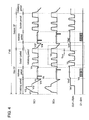
- FIG. 6 is a drawing showing a driving voltage waveform applied to data electrode 32 and scan electrode 22 and the voltage difference between data electrode 32 and scan electrode 22 , that is, (driving voltage waveform applied to the data electrode)-(driving voltage waveform applied to the scan electrode), in Embodiment 1 of the present invention.
- initializing voltage Vi 4 is set to be voltage value Vi 4 H
- the amplitude of the scan pulse voltage (Vc ⁇ Va) is abbreviated as Vscn in the following.
- the voltage applied to data electrode 32 is 0 V, and the voltage applied to scan electrode 22 is Vi 4 H. Therefore, the voltage difference between data electrode 32 and scan electrode 22 is equal to ( ⁇ Vi 4 H).
- the voltage in which the wall voltage is added to this voltage difference is almost equal to the discharge initial voltage. This is obvious also from that a weak initializing discharge is generated between data electrode 32 and scan electrode 22 in the initializing period till time tA. Therefore, the voltage difference between data electrode 32 and scan electrode 22 ( ⁇ Vi 4 H) is a voltage difference at the very limit of whether the discharge is initiated or not (in the following, this voltage difference is described as a “discharge lowest voltage”).
- the voltage difference between data electrode 32 and scan electrode 22 must exceed a voltage higher than the discharge lowest voltage ( ⁇ Vi 4 H) by prescribed voltage difference (in the following, this voltage difference is described as a “discharge stable voltage”) VA. That is, Vd ⁇ Vi 4 H+Vset 2 > ⁇ Vi 4 H+VA. That is, writing pulse voltage Vd must be Vd>VA ⁇ Vset 2 (Formula 1).
- the voltage difference between data electrode 32 and scan electrode 22 becomes (Vd ⁇ Vc) because voltage Vc is applied to scan electrode 22 and writing pulse voltage Vd is applied to data electrode 32 .
- the voltage difference between data electrode 32 and scan electrode 22 must be lower than the discharge lowest voltage ( ⁇ Vi 4 H) so that an unnecessary discharge is not generated. That is, Vd ⁇ Vc ⁇ Vi 4 H.
- the wall charges decrease by the influence of priming, an apparent dark current flows, and the wall voltage may decrease.
- the time during which writing pulse voltage Vd is applied to data electrode 32 becomes long when the ratio of the discharge cell that generates emission to all discharge cells (in the following, described as a “lighting ratio”) is high, the time during which the dark current flows becomes long. Therefore, in order to suppress this decrease in the wall charge, there is a necessity of making the dark current itself small.
- the voltage difference between data electrode 32 and scan electrode 22 must be lower by prescribed voltage (in the following, this voltage is described as a “non-discharge voltage”) VB than the discharge lowest voltage ( ⁇ Vi 4 H) even when writing pulse voltage Vd is applied to data electrode 32 . That is, Vd ⁇ Vc ⁇ Vi 4 H ⁇ VB. Therefore, Vd ⁇ Vc ⁇ (Va+Vset 2 ) ⁇ VB, that is, it must be Vscn>Vset 2+ VB+Vd (Formula 2).
- Vd>VA ⁇ Vset 2 (Formula 1) and Vscn>Vd+Vset 2+ VB (Formula 2) must be satisfied. Therefore, in order to make amplitude Vd of the writing pulse voltage small, it is favorable to set Vset 2 somewhat large. However, it must be at a level in which the address discharge is not generated in the case that scan pulse voltage Va is applied to scan electrode 22 and that writing pulse voltage Vd is not applied to data electrode 32 .
- FIG. 7 is a drawing showing one example of a driving voltage waveform applied to data electrode 32 and scan electrode 22 and the voltage difference between data electrode 32 and scan electrode 22 in the case that first SF can discharge more easily than second SF in Embodiment 1 of the present invention.
- discharge stable voltage VA ( 1 ) that is necessary to generate the stable address discharge in first SF becomes smaller than discharge stable voltage VA ( 2 ) in second SF, and non-discharge voltage VB ( 1 ) in first SF becomes larger than non-discharge voltage VB ( 2 ) in second SF.
- writing pulse voltage Vd ( 1 ) in first SF can be set lower than writing pulse voltage Vd ( 2 ) in second SF.
- writing pulse voltage Vd is set to higher writing pulse voltage Vd ( 2 ).
- Vd ( 1 ) is substituted for Vd ( 2 ) in (Formula 4) in (Formula 4)
- voltage Vc may be Vc ( 1 ) in which voltage Vc is increased by (Vd ( 2 ) ⁇ Vd ( 1 )) as shown in FIG. 8 .
- FIG. 8 is a drawing showing one example of a driving voltage waveform applied to data electrode 32 and scan electrode 22 and the voltage change between data electrode 32 and scan electrode 22 in the case that first SF can discharge more easily than second SF in Embodiment 1 of the present invention.
- Vscn of the scan pulse voltage becomes (Vc ( 1 ) ⁇ Va) and large, the driving power increases and there is a case that it leads to a cost increase such as to improve voltage resistance of a part used in the driving circuit.
- Vset 2 ( 1 ) in first SF is set to be small and initializing voltage Vi 4 is made to be voltage Vi 4 L.
- writing pulse voltage Vd can be set to be small without changing potential Vc of scan electrode 22 .
- FIG. 9 is a drawing showing another example of a driving voltage waveform applied to data electrode 32 and scan electrode 22 and the voltage change between data electrode 32 and scan electrode 22 in the case that first SF can discharge more easily than second SF in Embodiment 1 of the present invention.
- Vset 2 ( 1 ) >VB ( 2 ) and Vset 2 ( 1 ) ⁇ Vset 2 ( 2 ).
- Vscn ( 1 ) Vscn ( 2 )
- both amplitude Vd of the writing pulse voltage and amplitude Vscn of the scan pulse voltage can be made to be small as shown in FIG. 9 .
- both first SF and second SF generate a stable address discharge with the voltage between data electrode 32 and scan electrode 22 exceeding discharge stable voltages VA ( 1 ) and VA ( 2 ) at time tB, the voltage between data electrode 32 and scan electrode 22 is less than non-discharge voltages VB ( 1 ) and VB ( 2 ) at time tC, and an unnecessary discharge is not generated.
- each of writing pulse voltage Vd that is actually applied and amplitude Vscn of the scan pulse voltage can be set to be the minimum by adjusting the voltage of Vset 2 corresponding to the ease of the discharge as described above and by making the ease of the discharge of each subfield uniform.
- first SF is the all cell initializing subfield and sufficient priming is supplied in the address period of first SF
- first SF is considered to be the subfield where the discharge occurs the most easily. Therefore, from the reason described above, writing pulse voltage Vd and scan pulse voltage Va is considered to be set low by setting Vset 2 small in such subfield.
- the present Embodiment 1 is made to have a configuration of switching initializing voltage Vi 4 with Vi 4 L and Vi 4 H that is higher than Vi 4 L by switching Vset 2 corresponding to the luminance weight of the subfield, and stable writing is realized. That is, in the subfield with a small luminance weight (in the present Embodiment 1, first SF and second SF), as shown in FIG. 9 , the voltage of initializing voltage Vi 4 is decreased by making Vset 2 the voltage 0 V, the descending ramp waveform voltage is made to be a deep waveform, and the discharge period of the initializing discharge is made long.
- the wall voltage is decreased by strengthening the function of weakening the wall voltage on the top part of data electrodes D 1 to Dm, the deprivation of the wall charges of the discharge cell in the column that is not selected is decreased, and a stable writing operation is made to be performed.
- the voltage of initializing voltage Vi 4 is increased by making Vset 2 a prescribed voltage (in the present Embodiment 1, 10 V), the descending ramp waveform voltage is made to be a shallow waveform, and the discharge period of the initializing discharge is made short.
- the wall voltage is increased by increasing the remaining amount of the wall charges on the top part of data electrodes D 1 to Dm, the relative value of writing pulse voltage Vd to the discharge initial voltage is increased, and a stable address discharge is generated.
- the subfield in which a voltage of initializing voltage Vi 4 is Vi 4 L is defined as first SF and second SF and that the subfield in which a voltage of initializing voltage Vi 4 is Vi 4 H is defined as third SF to tenth SF.
- subfield Vset 2 In order to investigate in which subfield Vset 2 should be set low, that is, what subfield configuration is appropriate for performing the switching of initializing voltage Vi 4 the most suitably, the present inventor performed an experiment to investigate scan pulse voltage Va and writing pulse voltage Vd that are necessary to perform the stable writing while changing the subfield in which the switching of initializing voltage Vi 4 is performed.
- this experiment one field is divided into 10 subfields (first SF to tenth SF), and the luminance weights of (1, 2, 3, 6, 11, 18, 30, 44, 60, 80) are given to each subfield.
- Vi 4 L is made to be a voltage equal to scan pulse voltage Va by making Vset 2 to a voltage 0 V
- Vi 4 H is made to be a voltage higher than Vi 4 L by 10 V by making Vset 2 to a prescribed voltage (10 V in the present Embodiment 1).
- FIGS. 10A and 10B are drawings in which the results of this experiment are summarized, and are drawings showing the relationship between a subfield that switches initializing voltage Vi 4 and scan pulse voltage Va, and writing pulse voltage Vd.
- the x-axis shows an initializing voltage Vi 4 switching subfield
- the y-axis in FIG. 10A shows scan pulse voltage Va
- the y-axis in FIG. 10B shows writing pulse voltage Vd.
- Initializing voltage Vi 4 switching subfield here represents the subfield in which initializing voltage Vi 4 is switched from Vi 4 L to Vi 4 H, and for example, “2” of initializing voltage Vi 4 switching subfield shows that initializing voltage Vi 4 is made to be Vi 4 L in first SF and second SF and that initializing voltage Vi 4 is made to be Vi 4 H in third SF to tenth SF.
- initializing voltage Vi 4 switching subfield is “0” (initializing voltage Vi 4 is made to be Vi 4 H in all subfields), “1”, or “2”, scan pulse voltage Va that is necessary to perform the stable writing operation hardly changes. However, on and after that, as initializing voltage Vi 4 switching subfield is made larger, scan pulse voltage Va that is necessary to perform a stable writing operation gradually becomes high. Then, at initializing voltage Vi 4 switching subfield “10” (initializing voltage Vi 4 is made to be Vi 4 L in all subfields), scan pulse voltage Va that is necessary to perform a stable writing operation is about 20 V higher compared to initializing voltage Vi 4 switching subfield “2”.
- Vi 4 L is made to be a voltage equal to scan pulse voltage Va
- Vi 4 H is made to be a voltage higher than Vi 4 L by 10 V
- initializing voltage Vi 4 switching subfield is made to be “2”, that is, initializing voltage Vi 4 is made to be Vi 4 L in first SF that is a subfield with the smallest luminance weight and second SF that is a subfield with the second smallest luminance weight
- initializing voltage Vi 4 is made to be Vi 4 H in third SF to tenth SF including tenth SF that is a subfield with the largest luminance weight.
- scan pulse voltage Va actually applied to scan electrodes SC 1 to SCn and writing pulse voltage Vd actually applied to data electrodes D 1 to Dm are increased relative to scan pulse voltage Va and writing pulse voltage Vd that are necessary to perform the stable writing, and a stable writing can be realized.
- Vi 4 L, Vi 4 H, initializing voltage Vi 4 switching subfield, the subfield configuration, and the like are not limited to the above-described values, and they are desirably set to the optimal values by adapting to characteristics of the panel, specifications of the plasma display device, and the like.
- initializing voltage Vi 4 in the all cell initializing operation is described.
- Various methods can be considered to change initializing voltage Vi 4 .
- it can be realized by making voltage Vi 4 higher and lower by controlling steepness of the descending slope from voltage Vi 3 to voltage Vi 4 in FIG. 4 .
- One example of the method of controlling initializing voltage Vi 4 in the present Embodiment 1 is described with reference to a drawing.
- a controlling method of initializing voltage Vi 4 is described using the driving waveform at the all cell initializing operation as an example here.
- initializing voltage Vi 4 can be controlled by the same controlling method in the selected initializing operation.
- FIG. 11 is a circuit drawing of scan electrode driving circuit 53 in Embodiment 1 of the present invention.
- Scan electrode driving circuit 53 is equipped with sustain pulse generating circuit 100 that generates the sustain pulse, initializing waveform generating circuit 300 that generates the initializing waveform, and scan pulse generating circuit 400 that generates the scan pulse.
- Sustain pulse generating circuit 100 has power collecting circuit 110 to collect and reuse power when driving scan electrode 22 , switching element SW 1 to cramp scan electrode 22 to voltage Vs, and switching element SW 2 to cramp scan electrode 22 to the voltage 0 V.
- Initializing waveform generating circuit 300 is equipped with Miller integration circuits 310 and 320 , generates the above-described initializing waveform, and at the same time, perform a control of initializing voltage Vi 4 in the all cell initializing operation.
- Miller integration circuit 310 has FET 1 , capacitor C 1 , and resistance R 1 , and generates the ascending ramp waveform voltage gradually increasing in a ramp shape to voltage Vi 2 .
- Miller integration circuit 320 has FET 2 , capacitor C 2 , and resistance R 2 , and generates the descending ramp waveform voltage gradually decreasing in a ramp shape to prescribed initializing voltage Vi 4 .
- Each input terminal of Miller integration circuits 310 and 320 are shown as input terminal IN 1 and input terminal IN 2 .
- the Miller integration circuit is adopted using an FET that is practical as initializing waveform generating circuit 300 and whose configuration is relatively simple. However, it is not limited to this configuration, and may be any circuit as long as it is a circuit that is capable of generating the ascending ramp waveform voltage and the descending ramp waveform voltage.
- Scan pulse generating circuit 400 is equipped with switching elements S 31 and S 32 and Scan IC, selects one of the voltage applied to a main current line (a current line shown in a broken line in the drawing where sustain pulse generating circuit 100 , initializing waveform generating circuit 300 , and scan pulse generating circuit 400 are commonly connected) and the voltage in which voltage Vscn is superposed on the voltage of the main current line, and applies to the scan electrode.
- a main current line a current line shown in a broken line in the drawing where sustain pulse generating circuit 100 , initializing waveform generating circuit 300 , and scan pulse generating circuit 400 are commonly connected
- negative scan pulse voltage Va is generated in the address period by keeping the voltage of the main current line to negative voltage Va, switching negative voltage Va input to Scan IC with voltage Vc in which voltage Vscn is superposed on negative voltage Va, and outputting the voltage.
- Scan pulse generating circuit 400 outputs the voltage waveform of sustain pulse generating circuit 100 as it is in the sustain period.
- the above-described switching elements and Scan IC consist of an element such as a generally known MOSFET for performing a switching operation, and the switching is controlled based on the timing signal output from timing generating circuit 55 .
- scan electrode driving circuit 53 is equipped with AND gate AG that performs logic AND operation and comparator CP that compares the magnitude of the input signal that is input into two input terminals.
- Comparator CP compares the voltage (Va+Vset 2 ) in which voltage Vset 2 is superposed on voltage Va and the voltage of the main current line, outputs “0” in the case that the voltage of the main current line is higher, and “1” in other cases.
- Two input signals that is, output signal CEL 1 of comparator CP and switching signal CEL 2 , are input to AND gate AG.
- a timing signal output from timing generating circuit 55 can be used as switching signal CEL 2 .
- AND gate AG outputs “1” in the case that all of the input signals are “1”, and outputs “0” in other cases.
- the output of AND gate AG is input into scan pulse generating circuit 400 , and scan pulse generating circuit 400 outputs the voltage of the main current line if the output of AND gate AG is “0”, and outputs the voltage in which voltage Vscn is superposed on the voltage of the main current line if the output of AND gate AG is “1”.
- initializing waveform generating circuit 300 is described. First, the operation in the case that initializing voltage Vi 4 is made to be Vi 4 L is described with reference to FIG. 12 , and then the operation in the case that initializing voltage Vi 4 is made to be Vi 4 H is described with reference to FIG. 13 .
- the description about the all cell initializing period is made in FIGS. 12 and 13 . However, the descending ramp waveform voltage in the selected initializing period can be generated with the same operation as the description here. Further, in FIGS. 12 and 13 , the driving voltage waveform that performs the all cell initializing operation is divided into four periods represented by period T 1 to period T 4 , and each period is described.
- FIG. 12 is a timing chart to illustrate one example of the operation of scan electrode driving circuit 53 of the all cell initializing period in Embodiment 1 of the present invention.
- switching signal CEL 2 is kept to “0” in period T 1 to period T 4 , and the voltage waveform of initializing waveform generating circuit 300 is output as it is from scan pulse generating circuit 400 .
- switching element SW 1 in sustain pulse generating circuit 100 is made to be on. Then, voltage Vs is applied to scan electrode 22 through switching element SW 1 . After that, switching element SW 1 is made to be off.
- input terminal IN 1 of Miller integration circuit 310 is made to be a “high level”. Specifically, a voltage of 15 V is applied to input terminal IN 1 , for example. Then, a constant current flows from resistance R 1 toward capacitor C 1 , the source voltage of FET 1 rises in a ramp shape, and the output voltage of scan electrode driving circuit 53 also starts rising in a ramp shape. Then, this voltage rise sustains while input terminal IN 1 is at a “high level”.
- the ascending ramp waveform voltage gradually increasing from voltage Vs that is the discharge initial voltage or less (in the present Embodiment 1, it is equal to voltage Vi 1 , voltage Vi 3 , and voltage Vi 3 ′) toward voltage Vi 2 exceeding the discharge initial voltage is applied to scan electrode 22 .
- switching element SW 1 of sustain pulse generating circuit 100 is made to be on. Then, the voltage of scan electrode 22 decreases to voltage Vs. After that, switching element SW 1 is made to be off.
- input terminal IN 2 of Miller integration circuit 320 is made to be a “high level”. Specifically, a voltage of 15 V is applied to input terminal IN 2 , for example. Then, a constant current flows from resistance R 2 toward capacitor C 2 , the drain voltage of FET 2 falls in a ramp shape, and the output voltage of scan electrode driving circuit 53 also starts falling in a ramp shape. Then, after the output voltage reaches to prescribed negative voltage Vi 4 , input terminal IN 2 is made to be a “low level”.
- this descending ramp waveform voltage (the voltage of the main current line) is compared with the voltage (Va+Vset 2 ) in which voltage Vset 2 is added to voltage Va, and the output signal from comparator CP switches from “0” to “1” at time t 4 when the descending ramp waveform voltage becomes the voltage (Va+Vset 2 ) or less.
- switching signal CEL 2 is kept to “0” in period T 1 to period T 4 , “0” is output from AND gate AG. Therefore, this descending ramp waveform voltage is outputted as it is from scan pulse generating circuit 400 .
- the present Embodiment 1 does not switch to the subsequent address period by ending the initializing period right after the descending ramp waveform voltage has completely decreased to negative voltage Va, and period T 4 is set so that a period when it is kept to negative voltage Va, that is, period T 4 ′ when the initializing waveform is kept flat, is provided.
- period T 4 ′ is set to be about 20 ⁇ sec.
- the ascending ramp waveform voltage gradually increasing from voltage Vi 1 that is the discharge initial voltage or less toward voltage Vi 2 exceeding the discharge initial voltage is applied to scan electrode 22 , and after that, the descending ramp waveform voltage gradually decreasing from voltage Vi 3 toward initializing voltage Vi 4 L is applied.
- the voltage of the main current line is kept at negative voltage Va.
- the output signal from comparator CP is kept to “1”.
- switching signal CEL 2 is made to be “1”.
- the input of AND gate AG becomes also “1”, and “1” is output from AND gate AG.
- voltage Vc in which voltage Vscn is superposed on negative voltage Va is output from scan pulse generating circuit 400 .
- the output signal of AND gate AG becomes “0” by making switching signal CEL 2 “0” at the timing of generating the negative scan pulse voltage, and negative voltage Va is outputted from scan pulse generating circuit 400 . In such way, the negative scan pulse voltage in the address period can be generated.
- FIG. 13 is a timing chart to illustrate another example of the operation of scan electrode driving circuit 53 of an all cell initializing period in Embodiment 1 of the present invention.
- switching signal CEL 2 is made to be “1” in period T 1 to period T 4 .
- period T 4 is described here.
- input terminal IN 2 of Miller integration circuit 320 is made to be a “high level”. Specifically, a voltage of 15 V is applied to input terminal IN 2 , for example. Then, a constant current flows from resistance R 2 toward capacitor C 2 , the drain voltage of FET 2 falls in a ramp shape, and the output voltage of scan electrode driving circuit 53 also starts falling in a ramp shape. Then, after the output voltage reaches prescribed negative voltage Vi 4 , input terminal IN 2 is made to be a “low level”.
- this descending ramp waveform voltage (the voltage of the main current line) is compared with voltage (Va+Vset 2 ) in which voltage Vset 2 is added to voltage Va, and the output signal from comparator CP switches from “0” to “1” at time t 4 when the descending ramp waveform voltage becomes voltage (Va+Vset 2 ) or less. Then, because switching signal CEL 2 at this time is “1”, the input of AND gate also becomes “1”, and “1” is output from AND gate AG. With this, the voltage in which voltage Vscn is superposed on this descending ramp wave form voltage is output from scan pulse generating circuit 400 . Therefore, the lowest voltage in this descending ramp waveform voltage can be made to be (Va+Vset 2 ), that is, Vi 4 H.
- the lowest voltage of the gradually decreasing descending ramp waveform voltage that is, a value of initializing voltage Vi 4
- the lowest voltage of the gradually decreasing descending ramp waveform voltage that is, a value of initializing voltage Vi 4
- initializing voltage Vi 4 in the all cell initializing operation is described in the present Embodiment 1.
- the generation of the descending ramp waveform voltage in the selected initializing operation is the same operation as described above only with a different point that the ascending ramp waveform voltage is not generated, and the control of initializing voltage Vi 4 can be performed in the same way.
- the xenon partial pressure of the discharge gas is made to be 10%.
- the driving voltage may be set in accordance with the panel.
- each specific value used in the present Embodiment 1 is nothing but one example, and it is desirable to appropriately set optimal values by adapting to characteristics of the panel, specifications of the plasma display device, and the like.
- the drive method of a panel and the plasma display device of the present invention can generate a stable address discharge without making a voltage necessary to generate the address discharge high even in a large screen and a high luminance panel, and are useful as a drive method of a panel with a good image display quality and a plasma display device.
Landscapes
- Engineering & Computer Science (AREA)
- Physics & Mathematics (AREA)
- Plasma & Fusion (AREA)
- Power Engineering (AREA)
- Computer Hardware Design (AREA)
- General Physics & Mathematics (AREA)
- Theoretical Computer Science (AREA)
- Control Of Indicators Other Than Cathode Ray Tubes (AREA)
- Control Of Gas Discharge Display Tubes (AREA)
Abstract
Description
-
- 1 PLASMA DISPLAY DEVICE
- 10 PANEL
- 21 GLASS FRONT SUBSTRATE
- 22 SCAN ELECTRODE
- 23 SUSTAIN ELECTRODE
- 24, 33 DIELECTRIC LAYER
- 25 PROTECTIVE LAYER
- 28 DISPLAY ELECTRODE PAIR
- 31 REAR SUBSTRATE
- 32 DATA ELECTRODE
- 34 BARRIER RIB
- 35 PHOSPHOR LAYER
- 51 IMAGE SIGNAL PROCESS CIRCUIT
- 52 DATA ELECTRODE DRIVING CIRCUIT
- 53 SCAN ELECTRODE DRIVING CIRCUIT
- 54 SUSTAIN ELECTRODE DRIVING CIRCUIT
- 55 TIMING GENERATING CIRCUIT
- 100, 200 SUSTAIN PULSE GENERATING CIRCUIT
- 110 POWER COLLECTING CIRCUIT
- 300 INITIALIZING WAVEFORM GENERATING CIRCUIT
- 310, 320 MILLER INTEGRATION CIRCUIT
- 400 SCAN PULSE GENERATING CIRCUIT
- SW1, SW2, S31, S32 SWITCHING ELEMENT
- FET1, FET2 FET
- C1, C2 CAPACITOR
- R1, R2 RESISTANCE
- IN1, IN2 INPUT TERMINAL
- CP COMPARATOR
- AG AND GATE
Vd>VA−Vset2 (Formula 1).
Vscn>Vset2+VB+Vd (Formula 2).
Vd>VA−Vset2 (Formula 1) and
Vscn>Vd+Vset2+VB (Formula 2)
must be satisfied. Therefore, in order to make amplitude Vd of the writing pulse voltage small, it is favorable to set Vset2 somewhat large. However, it must be at a level in which the address discharge is not generated in the case that scan pulse voltage Va is applied to scan
Vd(1)>VA(1)−Vset2(1) (Formula 3) and
Vscn(1)>Vd(1)+Vset2(1)+VB(1) (Formula 4),
and for second SF,
Vd(2)>VA(2)−Vset2(2) (Formula 5) and
Vscn(2)>Vd(2)+Vset2(2)+VB(2) (Formula 6).
VA(2)−VA(1)=Vset2(2)−Vset2(1) (Formula 7), from
Vd(1)>VA(1)−Vset2(1) (Formula 3) and
Vd(2)>VA(2)−Vset2(2) (Formula 5),
it is possible to establish Vd (1)=Vd (2).
VB(1)−VB(2)=Vset2(2)−Vset2(1) (Formula 8), from
Vscn(1)>Vd(1)+Vset2(1)+VB(1) (Formula 4) and
Vscn(2)>Vd(2)+Vset2(2)+VB(2) (Formula 6),
it is possible to establish Vscn (1)=Vscn (2), and both amplitude Vd of the writing pulse voltage and amplitude Vscn of the scan pulse voltage can be made to be small as shown in
Claims (2)
Applications Claiming Priority (3)
| Application Number | Priority Date | Filing Date | Title |
|---|---|---|---|
| JP2006051735 | 2006-02-28 | ||
| JP2006-051735 | 2006-02-28 | ||
| PCT/JP2007/053507 WO2007099904A1 (en) | 2006-02-28 | 2007-02-26 | Plasma display panel drive method and plasma display device |
Publications (2)
| Publication Number | Publication Date |
|---|---|
| US20090231317A1 US20090231317A1 (en) | 2009-09-17 |
| US8081144B2 true US8081144B2 (en) | 2011-12-20 |
Family
ID=38459011
Family Applications (1)
| Application Number | Title | Priority Date | Filing Date |
|---|---|---|---|
| US12/088,762 Expired - Fee Related US8081144B2 (en) | 2006-02-28 | 2007-02-26 | Plasma display panel drive method and plasma display device |
Country Status (6)
| Country | Link |
|---|---|
| US (1) | US8081144B2 (en) |
| EP (1) | EP1947631A4 (en) |
| JP (1) | JP4655150B2 (en) |
| KR (1) | KR100938313B1 (en) |
| CN (1) | CN101351833B (en) |
| WO (1) | WO2007099904A1 (en) |
Families Citing this family (6)
| Publication number | Priority date | Publication date | Assignee | Title |
|---|---|---|---|---|
| CN101454819B (en) * | 2006-12-13 | 2011-04-13 | 松下电器产业株式会社 | Plasma display device and method for driving plasma display panel |
| US8294635B2 (en) * | 2007-01-12 | 2012-10-23 | Panasonic Corporation | Plasma display device and driving method of plasma display panel |
| JP5245282B2 (en) * | 2007-04-25 | 2013-07-24 | パナソニック株式会社 | Plasma display apparatus and driving method of plasma display panel |
| WO2009031272A1 (en) * | 2007-09-03 | 2009-03-12 | Panasonic Corporation | Plasma display panel driving apparatus, driving method and plasma display device |
| KR20120053529A (en) * | 2009-10-13 | 2012-05-25 | 파나소닉 주식회사 | Plasma display device drive method, plasma display device and plasma display system |
| KR20240095740A (en) | 2022-12-19 | 2024-06-26 | 박준오 | Curved bedhead with image and sound reproduction |
Citations (12)
| Publication number | Priority date | Publication date | Assignee | Title |
|---|---|---|---|---|
| EP1022715A2 (en) * | 1999-01-22 | 2000-07-26 | Matsushita Electric Industrial Co., Ltd. | Method of driving AC plasma display panel |
| JP2000242224A (en) | 1999-02-22 | 2000-09-08 | Matsushita Electric Ind Co Ltd | Method for driving ac type plasma display panel |
| JP2000267625A (en) | 1998-11-13 | 2000-09-29 | Matsushita Electric Ind Co Ltd | Gas discharge panel display device and gas discharge panel driving method |
| JP2002014650A (en) | 2000-06-28 | 2002-01-18 | Nec Corp | Ac type plasma display driving method |
| US20030189533A1 (en) * | 2002-04-04 | 2003-10-09 | Lg Electronics Inc. | Method for driving plasma display panel |
| US20030201726A1 (en) * | 2000-03-14 | 2003-10-30 | Lg Electronics Inc. | Method and apparatus for driving plasma display panel using selective write and selective erase |
| JP2004109838A (en) | 2002-09-20 | 2004-04-08 | Nec Corp | Driving method of ac type plasma display panel |
| US20040080280A1 (en) | 1998-11-13 | 2004-04-29 | Junichi Hibino | High resolution and high luminance plasma display panel and drive method for the same |
| US20050110713A1 (en) * | 2003-11-26 | 2005-05-26 | Woo-Joon Chung | Driving method of plasma display panel and display device thereof |
| EP1550998A2 (en) | 2003-12-31 | 2005-07-06 | Lg Electronics Inc. | Method and apparatus for driving plasma display panel |
| US20060290599A1 (en) * | 2005-06-24 | 2006-12-28 | Lg Electronics Inc. | Plasma display apparatus and driving method thereof |
| US20070152916A1 (en) * | 2006-01-05 | 2007-07-05 | Lg Electronics Inc. | Plasma Display Apparatus |
Family Cites Families (3)
| Publication number | Priority date | Publication date | Assignee | Title |
|---|---|---|---|---|
| CN1319037C (en) * | 2001-05-30 | 2007-05-30 | 松下电器产业株式会社 | Plamsa display panel display device and its driving method |
| DE10224181B4 (en) * | 2001-06-04 | 2010-02-04 | Samsung SDI Co., Ltd., Suwon | Method for resetting a plasma display |
| WO2003085780A1 (en) * | 2002-04-04 | 2003-10-16 | Molex Incorporated | Tri-band antenna |
-
2007
- 2007-02-26 KR KR1020087007811A patent/KR100938313B1/en not_active IP Right Cessation
- 2007-02-26 JP JP2008502770A patent/JP4655150B2/en not_active Expired - Fee Related
- 2007-02-26 CN CN2007800010919A patent/CN101351833B/en not_active Expired - Fee Related
- 2007-02-26 EP EP07714939A patent/EP1947631A4/en not_active Withdrawn
- 2007-02-26 US US12/088,762 patent/US8081144B2/en not_active Expired - Fee Related
- 2007-02-26 WO PCT/JP2007/053507 patent/WO2007099904A1/en active Application Filing
Patent Citations (15)
| Publication number | Priority date | Publication date | Assignee | Title |
|---|---|---|---|---|
| JP2000267625A (en) | 1998-11-13 | 2000-09-29 | Matsushita Electric Ind Co Ltd | Gas discharge panel display device and gas discharge panel driving method |
| US20040080280A1 (en) | 1998-11-13 | 2004-04-29 | Junichi Hibino | High resolution and high luminance plasma display panel and drive method for the same |
| EP1022715A2 (en) * | 1999-01-22 | 2000-07-26 | Matsushita Electric Industrial Co., Ltd. | Method of driving AC plasma display panel |
| JP2000242224A (en) | 1999-02-22 | 2000-09-08 | Matsushita Electric Ind Co Ltd | Method for driving ac type plasma display panel |
| US20030201726A1 (en) * | 2000-03-14 | 2003-10-30 | Lg Electronics Inc. | Method and apparatus for driving plasma display panel using selective write and selective erase |
| JP2002014650A (en) | 2000-06-28 | 2002-01-18 | Nec Corp | Ac type plasma display driving method |
| US20020050794A1 (en) | 2000-06-28 | 2002-05-02 | Nec Corporation | Method for driving AC plama display |
| US20030189533A1 (en) * | 2002-04-04 | 2003-10-09 | Lg Electronics Inc. | Method for driving plasma display panel |
| JP2004109838A (en) | 2002-09-20 | 2004-04-08 | Nec Corp | Driving method of ac type plasma display panel |
| US20050110713A1 (en) * | 2003-11-26 | 2005-05-26 | Woo-Joon Chung | Driving method of plasma display panel and display device thereof |
| KR20050050826A (en) | 2003-11-26 | 2005-06-01 | 삼성에스디아이 주식회사 | Driving method of plasma display panel and plasma display device |
| EP1550998A2 (en) | 2003-12-31 | 2005-07-06 | Lg Electronics Inc. | Method and apparatus for driving plasma display panel |
| US20060290599A1 (en) * | 2005-06-24 | 2006-12-28 | Lg Electronics Inc. | Plasma display apparatus and driving method thereof |
| US20070152916A1 (en) * | 2006-01-05 | 2007-07-05 | Lg Electronics Inc. | Plasma Display Apparatus |
| EP1806719A2 (en) | 2006-01-05 | 2007-07-11 | LG Electronics Inc. | Plasma display apparatus |
Non-Patent Citations (2)
| Title |
|---|
| International Search Report for PCT/JP2007/053507, dated Apr. 3, 2007. |
| Supplementary European Search Report for Application No. EP 07 71 4939, Nov. 2, 2009, Panasonic Corportion. |
Also Published As
| Publication number | Publication date |
|---|---|
| WO2007099904A1 (en) | 2007-09-07 |
| EP1947631A4 (en) | 2009-12-02 |
| JP4655150B2 (en) | 2011-03-23 |
| CN101351833A (en) | 2009-01-21 |
| CN101351833B (en) | 2011-07-13 |
| KR20080042915A (en) | 2008-05-15 |
| JPWO2007099904A1 (en) | 2009-07-16 |
| EP1947631A1 (en) | 2008-07-23 |
| KR100938313B1 (en) | 2010-01-22 |
| US20090231317A1 (en) | 2009-09-17 |
Similar Documents
| Publication | Publication Date | Title |
|---|---|---|
| JP4655090B2 (en) | Plasma display panel driving method and plasma display device | |
| US8081144B2 (en) | Plasma display panel drive method and plasma display device | |
| US8400372B2 (en) | Plasma display device and method of driving plasma display panel | |
| US20110037755A1 (en) | Driving method of plasma display panel | |
| US8355017B2 (en) | Plasma display device and plasma display panel drive method | |
| US8384621B2 (en) | Plasma display device and method for driving plasma display panel | |
| CN101578646B (en) | Plasma display device, and method for driving plasma display panel | |
| JPWO2008059735A1 (en) | Plasma display panel driving method and plasma display device | |
| JP5093105B2 (en) | Plasma display apparatus and driving method of plasma display panel | |
| WO2010143404A1 (en) | Plasma display panel drive method and plasma display device | |
| WO2011052219A1 (en) | Plasma display panel driving method and plasma display device | |
| JPWO2008026436A1 (en) | Plasma display apparatus and driving method of plasma display panel | |
| WO2013046652A1 (en) | Method for driving plasma display panel and plasma display device | |
| WO2012035761A1 (en) | Method for driving plasma display device, and plasma display device | |
| JP2008122734A (en) | Method for driving plasma display panel | |
| JP2012247465A (en) | Method of driving plasma display panel, and plasma display panel | |
| JP2009251267A (en) | Plasma display device and method for driving plasma display panel | |
| JP2010266650A (en) | Driving method of plasma display panel, and plasma display device | |
| JP2011075616A (en) | Method of driving plasma display panel, and plasma display device | |
| JP2012037589A (en) | Driving method of plasma display panel, and plasma display device |
Legal Events
| Date | Code | Title | Description |
|---|---|---|---|
| AS | Assignment |
Owner name: MATSUSHITA ELECTRIC INDUSTRIAL CO., LTD., JAPAN Free format text: ASSIGNMENT OF ASSIGNORS INTEREST;ASSIGNORS:ORIGUCHI, TAKAHIKO;SHOJI, HIDEHIKO;UEDA, MITSUO;REEL/FRAME:021151/0313 Effective date: 20071213 |
|
| AS | Assignment |
Owner name: PANASONIC CORPORATION, JAPAN Free format text: CHANGE OF NAME;ASSIGNOR:MATSUSHITA ELECTRIC INDUSTRIAL CO., LTD.;REEL/FRAME:021818/0725 Effective date: 20081001 Owner name: PANASONIC CORPORATION,JAPAN Free format text: CHANGE OF NAME;ASSIGNOR:MATSUSHITA ELECTRIC INDUSTRIAL CO., LTD.;REEL/FRAME:021818/0725 Effective date: 20081001 |
|
| FEPP | Fee payment procedure |
Free format text: PAYOR NUMBER ASSIGNED (ORIGINAL EVENT CODE: ASPN); ENTITY STATUS OF PATENT OWNER: LARGE ENTITY |
|
| REMI | Maintenance fee reminder mailed | ||
| LAPS | Lapse for failure to pay maintenance fees | ||
| STCH | Information on status: patent discontinuation |
Free format text: PATENT EXPIRED DUE TO NONPAYMENT OF MAINTENANCE FEES UNDER 37 CFR 1.362 |
|
| FP | Lapsed due to failure to pay maintenance fee |
Effective date: 20151220 |