US8081035B2 - Electronic pulse generator and oscillator - Google Patents
Electronic pulse generator and oscillator Download PDFInfo
- Publication number
- US8081035B2 US8081035B2 US11/863,217 US86321707A US8081035B2 US 8081035 B2 US8081035 B2 US 8081035B2 US 86321707 A US86321707 A US 86321707A US 8081035 B2 US8081035 B2 US 8081035B2
- Authority
- US
- United States
- Prior art keywords
- signal
- path
- control
- oscillator
- phase
- Prior art date
- Legal status (The legal status is an assumption and is not a legal conclusion. Google has not performed a legal analysis and makes no representation as to the accuracy of the status listed.)
- Expired - Fee Related
Links
- 230000001902 propagating effect Effects 0.000 claims abstract description 10
- 230000005540 biological transmission Effects 0.000 claims description 71
- 239000004020 conductor Substances 0.000 claims description 57
- 238000000034 method Methods 0.000 claims description 38
- 230000010355 oscillation Effects 0.000 claims description 28
- 230000001747 exhibiting effect Effects 0.000 claims description 5
- 230000008929 regeneration Effects 0.000 claims description 5
- 238000011069 regeneration method Methods 0.000 claims description 5
- 230000002441 reversible effect Effects 0.000 claims description 2
- 230000003213 activating effect Effects 0.000 claims 3
- 229910052751 metal Inorganic materials 0.000 description 36
- 239000002184 metal Substances 0.000 description 36
- 238000010168 coupling process Methods 0.000 description 32
- 230000008878 coupling Effects 0.000 description 31
- 238000005859 coupling reaction Methods 0.000 description 31
- 239000010410 layer Substances 0.000 description 31
- 230000000694 effects Effects 0.000 description 29
- 230000001360 synchronised effect Effects 0.000 description 17
- 238000013461 design Methods 0.000 description 15
- 239000003990 capacitor Substances 0.000 description 13
- 230000008859 change Effects 0.000 description 12
- 238000011068 loading method Methods 0.000 description 12
- 230000008569 process Effects 0.000 description 11
- 238000009826 distribution Methods 0.000 description 10
- VYPSYNLAJGMNEJ-UHFFFAOYSA-N Silicium dioxide Chemical compound O=[Si]=O VYPSYNLAJGMNEJ-UHFFFAOYSA-N 0.000 description 9
- 230000001419 dependent effect Effects 0.000 description 9
- 230000006870 function Effects 0.000 description 9
- 230000009471 action Effects 0.000 description 8
- 238000006243 chemical reaction Methods 0.000 description 8
- 230000001965 increasing effect Effects 0.000 description 8
- 230000001939 inductive effect Effects 0.000 description 8
- 238000004519 manufacturing process Methods 0.000 description 8
- 238000001465 metallisation Methods 0.000 description 8
- 230000007704 transition Effects 0.000 description 8
- 230000008901 benefit Effects 0.000 description 7
- 230000015572 biosynthetic process Effects 0.000 description 7
- 238000005755 formation reaction Methods 0.000 description 7
- 230000003071 parasitic effect Effects 0.000 description 7
- 230000009467 reduction Effects 0.000 description 7
- 230000002457 bidirectional effect Effects 0.000 description 6
- 230000001427 coherent effect Effects 0.000 description 6
- 230000006872 improvement Effects 0.000 description 6
- 239000011159 matrix material Substances 0.000 description 6
- 230000001934 delay Effects 0.000 description 5
- 238000005516 engineering process Methods 0.000 description 5
- 238000012545 processing Methods 0.000 description 5
- 235000012239 silicon dioxide Nutrition 0.000 description 5
- 239000000758 substrate Substances 0.000 description 5
- 238000012546 transfer Methods 0.000 description 5
- 238000013459 approach Methods 0.000 description 4
- 239000011248 coating agent Substances 0.000 description 4
- 238000000576 coating method Methods 0.000 description 4
- 238000004891 communication Methods 0.000 description 4
- 230000002500 effect on skin Effects 0.000 description 4
- 230000008030 elimination Effects 0.000 description 4
- 238000003379 elimination reaction Methods 0.000 description 4
- 238000002347 injection Methods 0.000 description 4
- 239000007924 injection Substances 0.000 description 4
- 239000012212 insulator Substances 0.000 description 4
- 230000007246 mechanism Effects 0.000 description 4
- 238000004064 recycling Methods 0.000 description 4
- 239000004065 semiconductor Substances 0.000 description 4
- 238000000926 separation method Methods 0.000 description 4
- 230000011664 signaling Effects 0.000 description 4
- 239000000377 silicon dioxide Substances 0.000 description 4
- 238000012360 testing method Methods 0.000 description 4
- 229910000859 α-Fe Inorganic materials 0.000 description 4
- XUIMIQQOPSSXEZ-UHFFFAOYSA-N Silicon Chemical compound [Si] XUIMIQQOPSSXEZ-UHFFFAOYSA-N 0.000 description 3
- 238000010586 diagram Methods 0.000 description 3
- 230000003993 interaction Effects 0.000 description 3
- 230000010363 phase shift Effects 0.000 description 3
- 230000001172 regenerating effect Effects 0.000 description 3
- 238000012163 sequencing technique Methods 0.000 description 3
- 238000004088 simulation Methods 0.000 description 3
- 235000013290 Sagittaria latifolia Nutrition 0.000 description 2
- 238000010521 absorption reaction Methods 0.000 description 2
- 238000003491 array Methods 0.000 description 2
- 235000015246 common arrowhead Nutrition 0.000 description 2
- 238000010276 construction Methods 0.000 description 2
- 230000001276 controlling effect Effects 0.000 description 2
- 230000001808 coupling effect Effects 0.000 description 2
- 125000004122 cyclic group Chemical group 0.000 description 2
- 230000003247 decreasing effect Effects 0.000 description 2
- 239000003989 dielectric material Substances 0.000 description 2
- 238000009792 diffusion process Methods 0.000 description 2
- 230000005684 electric field Effects 0.000 description 2
- 238000003780 insertion Methods 0.000 description 2
- 230000037431 insertion Effects 0.000 description 2
- 238000009413 insulation Methods 0.000 description 2
- 238000002161 passivation Methods 0.000 description 2
- 230000035699 permeability Effects 0.000 description 2
- 230000000750 progressive effect Effects 0.000 description 2
- 230000006798 recombination Effects 0.000 description 2
- 238000005215 recombination Methods 0.000 description 2
- 238000011084 recovery Methods 0.000 description 2
- 230000001105 regulatory effect Effects 0.000 description 2
- 230000003014 reinforcing effect Effects 0.000 description 2
- 230000008054 signal transmission Effects 0.000 description 2
- 229910052710 silicon Inorganic materials 0.000 description 2
- 239000010703 silicon Substances 0.000 description 2
- 238000004513 sizing Methods 0.000 description 2
- 230000008719 thickening Effects 0.000 description 2
- 238000009966 trimming Methods 0.000 description 2
- 238000004804 winding Methods 0.000 description 2
- ZCJJIQHVZCFSGZ-UHFFFAOYSA-N 2,8-bis(diphenylphosphoryl)dibenzothiophene Chemical compound C=1C=CC=CC=1P(C=1C=C2C3=CC(=CC=C3SC2=CC=1)P(=O)(C=1C=CC=CC=1)C=1C=CC=CC=1)(=O)C1=CC=CC=C1 ZCJJIQHVZCFSGZ-UHFFFAOYSA-N 0.000 description 1
- RYGMFSIKBFXOCR-UHFFFAOYSA-N Copper Chemical compound [Cu] RYGMFSIKBFXOCR-UHFFFAOYSA-N 0.000 description 1
- 206010040844 Skin exfoliation Diseases 0.000 description 1
- 239000000654 additive Substances 0.000 description 1
- 230000000996 additive effect Effects 0.000 description 1
- 230000004075 alteration Effects 0.000 description 1
- PNEYBMLMFCGWSK-UHFFFAOYSA-N aluminium oxide Inorganic materials [O-2].[O-2].[O-2].[Al+3].[Al+3] PNEYBMLMFCGWSK-UHFFFAOYSA-N 0.000 description 1
- 230000003321 amplification Effects 0.000 description 1
- 238000004458 analytical method Methods 0.000 description 1
- 230000009286 beneficial effect Effects 0.000 description 1
- 230000033228 biological regulation Effects 0.000 description 1
- 238000009954 braiding Methods 0.000 description 1
- 230000000739 chaotic effect Effects 0.000 description 1
- 230000001447 compensatory effect Effects 0.000 description 1
- 239000002131 composite material Substances 0.000 description 1
- 239000012141 concentrate Substances 0.000 description 1
- 229910052802 copper Inorganic materials 0.000 description 1
- 239000010949 copper Substances 0.000 description 1
- 238000012937 correction Methods 0.000 description 1
- 238000006880 cross-coupling reaction Methods 0.000 description 1
- 239000013078 crystal Substances 0.000 description 1
- 230000009699 differential effect Effects 0.000 description 1
- 239000006185 dispersion Substances 0.000 description 1
- 230000009977 dual effect Effects 0.000 description 1
- 230000005288 electromagnetic effect Effects 0.000 description 1
- 230000005672 electromagnetic field Effects 0.000 description 1
- 238000005530 etching Methods 0.000 description 1
- 230000002349 favourable effect Effects 0.000 description 1
- 239000012634 fragment Substances 0.000 description 1
- 239000003574 free electron Substances 0.000 description 1
- 230000007274 generation of a signal involved in cell-cell signaling Effects 0.000 description 1
- 239000011521 glass Substances 0.000 description 1
- 230000010354 integration Effects 0.000 description 1
- 238000010884 ion-beam technique Methods 0.000 description 1
- 230000001788 irregular Effects 0.000 description 1
- 238000002955 isolation Methods 0.000 description 1
- 238000003698 laser cutting Methods 0.000 description 1
- 238000001459 lithography Methods 0.000 description 1
- 230000005415 magnetization Effects 0.000 description 1
- 238000005259 measurement Methods 0.000 description 1
- 238000004377 microelectronic Methods 0.000 description 1
- 238000003801 milling Methods 0.000 description 1
- 238000012544 monitoring process Methods 0.000 description 1
- 238000003199 nucleic acid amplification method Methods 0.000 description 1
- 230000003534 oscillatory effect Effects 0.000 description 1
- 238000013021 overheating Methods 0.000 description 1
- 238000000059 patterning Methods 0.000 description 1
- 229910021420 polycrystalline silicon Inorganic materials 0.000 description 1
- 229920000642 polymer Polymers 0.000 description 1
- 229920005591 polysilicon Polymers 0.000 description 1
- 238000002360 preparation method Methods 0.000 description 1
- 230000001737 promoting effect Effects 0.000 description 1
- 239000010453 quartz Substances 0.000 description 1
- 230000019681 resolution of meiotic recombination intermediates Effects 0.000 description 1
- 230000000630 rising effect Effects 0.000 description 1
- 238000012216 screening Methods 0.000 description 1
- 230000011218 segmentation Effects 0.000 description 1
- 229910052709 silver Inorganic materials 0.000 description 1
- 239000004332 silver Substances 0.000 description 1
- 239000002356 single layer Substances 0.000 description 1
- 239000007787 solid Substances 0.000 description 1
- 239000000243 solution Substances 0.000 description 1
- 238000001228 spectrum Methods 0.000 description 1
- 235000013599 spices Nutrition 0.000 description 1
- 238000004544 sputter deposition Methods 0.000 description 1
- 230000006641 stabilisation Effects 0.000 description 1
- 238000011105 stabilization Methods 0.000 description 1
- 230000009897 systematic effect Effects 0.000 description 1
- 230000002277 temperature effect Effects 0.000 description 1
- 230000009466 transformation Effects 0.000 description 1
- 239000002699 waste material Substances 0.000 description 1
- 230000010356 wave oscillation Effects 0.000 description 1
Images


Classifications
-
- H—ELECTRICITY
- H03—ELECTRONIC CIRCUITRY
- H03B—GENERATION OF OSCILLATIONS, DIRECTLY OR BY FREQUENCY-CHANGING, BY CIRCUITS EMPLOYING ACTIVE ELEMENTS WHICH OPERATE IN A NON-SWITCHING MANNER; GENERATION OF NOISE BY SUCH CIRCUITS
- H03B5/00—Generation of oscillations using amplifier with regenerative feedback from output to input
- H03B5/18—Generation of oscillations using amplifier with regenerative feedback from output to input with frequency-determining element comprising distributed inductance and capacitance
- H03B5/1841—Generation of oscillations using amplifier with regenerative feedback from output to input with frequency-determining element comprising distributed inductance and capacitance the frequency-determining element being a strip line resonator
- H03B5/1847—Generation of oscillations using amplifier with regenerative feedback from output to input with frequency-determining element comprising distributed inductance and capacitance the frequency-determining element being a strip line resonator the active element in the amplifier being a semiconductor device
- H03B5/1852—Generation of oscillations using amplifier with regenerative feedback from output to input with frequency-determining element comprising distributed inductance and capacitance the frequency-determining element being a strip line resonator the active element in the amplifier being a semiconductor device the semiconductor device being a field-effect device
-
- H—ELECTRICITY
- H01—ELECTRIC ELEMENTS
- H01L—SEMICONDUCTOR DEVICES NOT COVERED BY CLASS H10
- H01L2924/00—Indexing scheme for arrangements or methods for connecting or disconnecting semiconductor or solid-state bodies as covered by H01L24/00
- H01L2924/0001—Technical content checked by a classifier
- H01L2924/0002—Not covered by any one of groups H01L24/00, H01L24/00 and H01L2224/00
Definitions
- This invention concerns improvements in and relating to electronic production and use of repeating cyclic pulse signals having a repetition rate related to electrical signal path length(s).
- Suitable disclosed electronic circuitry includes composite electromagnetic/semiconductor structures for providing timing signals in integrated circuits (ICs), typically in clocking digital ICs, including VLSI (very large scale integrated) circuits.
- ICs integrated circuits
- VLSI very large scale integrated
- suitable such means includes at least one signal path exhibiting endless electromagnetic continuity and affording signal phase inversion of an electromagnetic wave type signal, and path-associated active means.
- preferred electromagnetic traveling wave recirculation of such endlessly electromagnetically continuous path can produce pulses with a repetition rate having a time constant related to and effectively defined by the electrical length of said signal path.
- Such endless signal paths are inherently unterminated so free of termination and reflection problems, and low impedance is not a problem as only “top-up” energy is required to maintain amplitude of pulse waveforms.
- Fast switching said path-associated active means is advantageous to direct production of highly square wave forms, with rise and fall times according to switching between voltage levels and spacings thus pulse duration according to transit of said signal path.
- Such operation can be viewed as effectively repeating traversal of said signal path by a voltage level transition that can be very fast, the transition being effectively inverted by its said signal path traversal.
- Suitable said signal path can be of transmission line nature, as realizable for ICs on an on-chip basis by such as microstrip, coplanar waveguide or stripline lithography using resist patterns and etching.
- Functional signal path implementation can be as substantially parallel double-loops with insulated cross-over formation, traceable as a substantially linear conductive formation of Mobius ring effect.
- Practical active means achieving signal top-up or regeneration can be as cross-coupled bidirectional amplifiers between such double-looped conductive formations, say using N-channel and P-channel mosfet transistor formations as for typical CMOS VLSI chips.
- Practical dielectric includes silicon dioxide, e.g. field oxide or inter-metal dielectrics, but substrate dielectrics are usable when of semi-insulating or SOI (semiconductor-on-insulator) nature.
- Rotary traveling wave clocking can be provided well into the plus- and plural-GHz frequency ranges even using current CMOS fabrication technology.
- the popular synchronous paradigm can be maintained, with such high frequencies available all over the chip areas by readily extendable plural frequency locked loops.
- PLL phase-lock loop
- the termination and reflection problems of conventional H-tree signal distribution do not apply; and there are predictable phases/phase relationships at all points (coherency), so clear practicality for moving away from the single-phase synchronous paradigm and its very high power spikes.
- electronic pulse generator or oscillator circuitry comprising a signal path exhibiting endless electromagnetic continuity affording signal phase inversion in setting pulse duration or half-cycles of oscillation within time of signal traverse of said signal path, and having active switching means associated with said signal path to set rise and fall times of each said pulse or said half-cycle of oscillation, is further characterized by one or more of the following:
- passivation layer say ferrite
- power supply including distribution and/or voltage charging and/or DC-AC and AC-DC conversion
- simultaneous two-way synchronous data transfer bus preferably in association with two physically separated but coherently synchronous clocks to control transmission and reception bits preferably on a two phase basis, has one or more of the following further provisions for
- varactor means associated with said signal path additionally to said active switching means say as differential mosfets with common high resistance control line—temperature and/or voltage compensator means associated with said signal path additionally to said active switching means, preferably as plural distributed compensators say as diffusion diodes—localized impedance variation for said signal path, say to counter heavy capacitance loading effects
- phase adjustment by means associated with said signal path additionally to said active switching means, say to compensate 4-phase logic timing signal components for skew from such as temperature effects
- One embodiment of the present invention is a multiphase electronic oscillator that includes a signal path, active switching means, and a control path.
- the signal path exhibits endless electric or magnetic continuity or both and includes a signal phase inversion that sets a half-cycle of oscillation of a signal traveling on the signal path according to the time the signal takes to traverse said path.
- the active switching means is associated with said signal path to set rise and fall times of each said half-cycle of oscillation.
- the control path is adjacent to and follows said signal path and propagates a control signal in a particular direction on the control path to activate each active switching means in the order of the direction of the control signal propagation, where the traveling control signal urges the signal on the signal path to travel in the direction of the propagation of the control signal.
- Another embodiment of the present invention is a method of starting a multiphase oscillator having a signal path exhibiting endless electric or magnetic continuity or both and including signal phase inversion that sets a half-cycle of oscillation of a signal traveling on the signal path according to the time the signal takes to traverse said path, active switching means associated with the signal path to set rise and fall times of each said half-cycle of oscillation, and a control path that is adjacent to and follows the signal path.
- the method includes (i) deactivating the active switching means, and (ii) then propagating a signal on the control path to activate in turn each active switching means in the order set by the direction of propagating of the signal on the control path.
- FIG. 1 is a circuit diagram for a pulse operation or oscillator
- FIG. 2 is a convenient simplified representation
- FIGS. 3 a, b indicate alternative directions of traveling wave rotation
- FIGS. 4 a, b show idealized differential waveforms and relationship between propagation delay and electrical/physical lengths of a transmission line
- FIGS. 5 a, b indicate alternatives by way of negative resistance switching means and single-ended operation, respectively;
- FIGS. 6 a - e indicate alternative coplanar loop or ring conductors
- FIGS. 7 a, b are useful regarding cross-talk with another signal path
- FIG. 8 shows tap-positions and interconnections of four loops or rings
- FIG. 9 shows symbolic representations, connections to logic, and interconnections for plural loops or rings and one rotation direction
- FIG. 10 shows further extension and interconnection between chips
- FIGS. 11 a - d show coupling correlation/reduction
- FIGS. 12 a - c show cross-conduction reduction and/or rotation direction bias
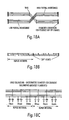
- FIGS. 13 a - d show flip-chip usage and/or rotation direction startup
- FIGS. 14 a - e show various circuit detail of latch, oscillator, counter, gating and regulator functions
- FIGS. 15 a - e show symbolic, schematic and equivalent circuitry
- FIGS. 16 a - d relate to power supply and conversion
- FIGS. 17 a - c relate to CAD layout work
- FIGS. 18 a - f concern dealing with skin, eddy and proximity effects
- FIGS. 19 a - g concern array and matrix synchronous input/output
- FIGS. 20 a & b concern capacitive compensation
- FIGS. 21 a - c concern heavy top-off loading
- FIGS. 22 a - d concern operation with reduced parasitics
- FIG. 23 concerns frequency switching
- FIG. 24 concerns phase adjustment for such as four-phase clocking of domino logic
- FIGS. 25 a - c concern frequency adjustment according to inductance and ways to increase inductance
- FIG. 26 concerns low power mode without stopping the clock/timing generation.
- FIG. 1 shows a transmission-line 15 as a structure that is physically as well as electromagnetically endless, specifically comprising a single continuous “originating” conductor formation 17 shown forming two appropriately spaced generally parallel traces as loops 15 a , 15 b with a cross-over at 19 that does not involve any local electrical connection of the conductor 17 .
- the length of the originating conductor 17 taken as S, corresponds to two ‘laps’ of the transmission-line 15 as defined between the spaced loop traces 15 a , 15 b and through the crossover 19 .
- the cross-over 19 produces a Moebius strip effect where edge traces of the loops 15 a , 15 b invert from lap to lap.
- the transmission-line 15 has associated plural spaced active means 21 conveniently of bi-directional switching/amplifying nature shown as two inverters 23 a , 23 b connected back-to-back between the conductive loop traces 15 a , 15 b .
- Alternative active regenerative means could rely on negative resistance, negative capacitance or be otherwise suitably non-linear, and regenerative (such as Gunn diodes).
- Respective input/output terminals of each circuit 21 are shown connected to the transmission-line 15 between the loops 15 a , 15 b at substantially maximum spacing apart along the effectively single conductor 17 , thus each at substantially halfway around the transmission-line 15 relative to the other.
- FIG. 2 shows convenient simplified/idealized representation that omits the active means 21 .
- These can be any odd number of cross-overs 19
- transmission line loop 15 can be any shape, including geometrically irregular, so long as they have a length appropriate to the desired operating frequency, i.e. so that a signal leaving an amplifier 21 arrives back inverted after a full ‘lap’ of the transmission-line 15 , traversed in a time Tp effectively defining a pulse width or half-cycle oscillation time of full-cycle bipolar operating frequency.
- Endless electromagnetic continuity of the transmission line 15 along with fast switching times of preferred transistors in the inverters 23 a and 23 b , leads to a strongly square wave-form containing odd harmonics of the fundamental frequency F effectively reinforced.
- the terminals of the amplifiers 21 appear substantially unloaded, due to the transmission-line 15 being ‘closed-loop’ without any form of termination, which results very desirably in low power dissipation and low drive requirements.
- the inductance and capacitance per unit length of the transmission-line 15 can be altered independently, as can also be desirable and advantageous.
- Coherent pulse/oscillation operation occurs when the signal in the transmission line meets this requirement for all connected inverters, so all inverters are working in a coordinated manner with known phase relationship between all points on the transmission line.
- This criterion is met only when there is a single rotating traveling wave in the line, i.e. rotating either clockwise or anticlockwise, see FIGS. 3A and 3B showing line current flow by arrow-heads, polarity by circled plus and minus signs, direction of rotation by full arrows, and phase from arbitrary 0/360 degree position, for a two-lap traverse of the path 15 .
- the wavefront incident a transistor overrides its previous drive direction due to low wave impedance compared to a single transistor.
- the transistors contribute to imposing the new wave polarity by reason of connecting the transmission line terminal to the correct power source polarity—which maintains ‘top-up’ energy to give constant amplitude in the presence of (mainly resistive) losses in the transmission line. Switching by the transistors also helps prevent the build-up of any counter-direction waves, effectively acting as wave gates.
- FIG. 4 a shows idealized waveforms for a switching amplifier 21 with inverters 23 a and 23 b .
- Component oscillation waveforms (D 1 , 02 appear at the input/output terminals of that amplifier 21 shortly after the ‘start-up’ phase, and continue during normal operation.
- These waveforms ( 1 i 1 and C′ 2 are substantially square and differential, i.e. two-phase inverse in being 180 degrees out-of-phase.
- These differential waveforms 01 and ' 2 cross substantially at the mid-point (V+/2) of the maximum signal amplitude (V+). This mid point (V+/2) can be considered as a ‘null’ point in a voltage level transition.
- this null point and voltage level transition effectively sweep round the transmission line 15 producing very fast rise and fall times in a very ‘clean’ square-wave form definition.
- FIG. 4 b shows relationships between the propagation delay or traverse time (Tp), electrical length in degrees, and physical length (S) of originating conductive line/trace 17 .
- Tp propagation delay or traverse time
- S physical length
- CMOS inverter symbol as used herein is a kind of shorthand.
- the number of Nch and Pch devices need not be the same, nor need they be co-located.
- the basic requirement is to distribute a number of small width devices along the path of the transmission-line connected appropriately.
- each device has an on-resistance substantially higher than the impedance of the transmission-line, while the total paralleled resistance of all devices is of the same order as the impedance of the line. This is to ensure the devices can be overridden by an incident wave and strong oscillation characteristics respectively.
- Alternatives to more common CMOS devices include Nch+ pull-ups, Pch+ pull-downs, Bipolar transistors, negative resistance devices (e.g. Gunn diode), or Mesfet etc., see FIG. 5A where there will be no cross-coupling other than by way of electromagnetic coupling.
- Single ended operation is also available between a conductor and AC ground as indicated in FIG. 513 , again showing an electromagnetically endless signal path 15 C with an inverting transmission line transformer 19 T and inverter latches, as active switching means 21 L, though their delay time is likely to affect frequency and the charge at the second inverter is not energy recycled as efficiently as above-preferred differential structure/operation.
- the transmission line 15 is readily implemented as co-planar strip by two parallel conductive traces, usually metal to those may be lower and/or upper conductive ground phase layers still allowing viable differential transmission line operation, but also affording common-mode propagation between each trace and AC ground.
- any method of signal inversion can be used, i.e. other than a cross-over, e.g. an inverting transmission line transformer.
- differential signal transmission mode coplanar strips and back-to-back inverters differential signals are output by the inverter pair with signal energy launched to the transmission line inductively and capacitively by magnetic and electric fields between the signal conductors as well as each signal conductor and ground (or two individual common-mode paths).
- FIG. 6A is a cross-section through a portion of one exemplary on-IC transmission-line formation comprising three metal layers 56 , 58 and 60 and two dielectric layers 62 and 64 .
- Middle metal layer 58 is illustrated as comprising the two transmission-line loop conductive traces 15 a and 15 b that are at least nominally parallel.
- Upper metal layer 60 could be used as an AC ‘ground’ plane and could be connected to the positive supply voltage V+, lower metal 56 being a ‘ground’ plane that could be connected to the negative supply voltage GND.
- the dielectric layers 62 and 64 between the metal transmission-line traces at 58 and ‘ground’ planes 56 and 58 are typically formed using silicon dioxide (SiO2).
- the full illustrated structure is seen as preferable, though may be not essential in practice, i.e. as to inclusion of either or both of the ‘ground’ planes and the dielectric layers 62 , 64 .
- the physical spacing 66 between the conductive traces 15 a , 15 b affects the differential and common modes of signal propagation, which should preferably have equal, or substantially equal, velocities in order to achieve minimum dispersion of the electromagnetic field from the spacing 66 . Screening properties improve with use of ‘ground planes’, as does the ability for the structure to drive non-symmetrical, i.e. unbalanced, loads applied to the conductive traces 15 a , 15 b .
- 6B-D show alternative coplanar 1 provisions believed to be largely self-evident for ground central ( 6 C) rather than flanking a signal pair ( 6 B), grounds flanking and central ( 6 D), and a multiple arrangement ( 6 E) with central ground split flanking a specific data line and flanking outer grounds, respectively.
- Non-planar layouts can be distributed between different layers of metallization with appropriate vies and straps (not shown).
- FIG. 7A shows that differential transmission line traces with a crossing signal path on another metal layer have little if any cross-talk effects as and where in co-parallel relation.
- FIG. 7B shows “twisted pair” type cross-oval in the differential transmission line traces to reduce cross-talk relative to a parallel other signal path, the cross-ovens being at intervals that relate to pulse direction between rise and fall times; with some increase in capacitance per unit length of the transmission line.
- FIGS. 8 and 9 show how multiple single rings can be ‘gridded’ to cover a large area. Each loop maintains the same frequency as when operated in isolation. Placement and locking interconnection of four rings as shown in FIG. 8 produces by default an inner ring. An arbitrary connection position code is indicated on a twenty per outer (A) and inner (B) line basis with loop suffixing (N, E, S, W). If such process is repeated, a configuration as in FIG. 9 can result in twice the area coverage because of the virtual rings formed (which as real and effective in practice as the actual rings). By virtue of the electrical connections between the rings, oscillation becomes phase-locked overall. As shown by the direction of the arrows, adjacent rings must have waves which rotate counter-clockwise to each other.
- FIG. 9 includes and uses simplified double-line loop/crossover and more generalized single-line indication with circled-X for any inverting element representation.
- FIG. 10 shows one example of coherent frequency and phase operation of two clock distribution networks of two monolithic ICs 68 1 , 68 2 each having a clock generation and distribution hereof and pairs of inter-IC connections E, F and G, FL
- the two ICs concerned will operate coherently, i.e. at the same frequency and with the same phase relationships, where each of the connections is substantially of 180-degrees electrical lengths, or a multiple satisfying 360°.n+180° where n is zero or an integer.
- a single pair of inter-IC connections (E, F or G, H) will result in frequency and phase ‘locking’.
- clock rings or loops can be passive or active, free wires cannot usefully be active and some active sections can serve to input energy. Kirchoff-like rules apply to signal or energy branching and combining.
- first and second ‘stub’ connections 82 and 83 are shown in FIG. 10 , though there could be more of either or each.
- the first stub connection 82 has a total electrical length of 90° to a short-circuit and is acceptable anywhere so long as not active.
- the second stub connection 83 is open-circuit and of 180° electrical length and can be helpful for stabilization.
- Such stubs 82 , 83 can be particularly useful for non-IC applications of the invention where conductive trace definition may be less precise than for ICs. Impedance of the pairs of connections E, F and G, II and connections 82 , 83 can have any value since, in normal operation and once these connections are energized, there will be no net power flow therein for correct phasing thereof.
- connections E, F and G, H and 82 , 83 is greater than that of oscillator transmission-lines 15 to which they are connected. These connections will support a standing EM wave rather than a traveling EM wave. Free wire interconnects can be of any characteristic impedance as no net power flows through them in normal operation at correct phasing (unlike the clock loops which circulate energy with directional rotation in normal operation).
- FIG. 10 inter-connections can be applied equally well to infra-IC, inter-IC, IC-to-PCB and/or any non-IC, i.e. PCB-to-PCB system connections.
- edge rates can be controlled in simple ways. One is to reduce the number of ‘top-up’ amplifiers keeping total transistor width constant, which gives a higher lumped-C effect at the amplifiers, larger series inductance between the amplifiers and therefore a natural distributed LC shunt tank circuit. This can be designed precisely for cut-off frequency to cut-off of the higher frequency harmonics in the otherwise square waveform, reducing the edge rate.
- Another way is to design all ‘tap’ connections from the main ring to have a return time-of-flight back to the ring of approximately the desired rise/fall times so those lines then act as frequency-selective stubs and inhibit rise/fall from occurring until the round-trip delay time of the tap has passed.
- Adjusting the thickness of the dielectric overcoat (overglass) on the wafer can adjust operating frequency, and is apposite to account for process variability. Typical thickness of ⁇ 1 u could be increased up to 5 u to increase the capacitance per unit length of the transmission lines located on top-metal Phase velocity will be slowed as more electric field lines are in dielectric (rather than in air).
- a wafer designed to run ‘too-slow’ by having maximum dielectric thickness can have the dielectric ‘etched-back’ to achieve the desired trimmed operating frequency. The amount of etch back required can be determined by pre testing the wafer to determine the change in permeability required.
- phase velocity is by ferrite coating above the top layer of passivation to alter the magnetic permeability of the medium surrounding the transmission-line conductors, say applied by sputtering.
- a subsequent mask-etch step could leave ferrite covering only those regions above clock lines. Other lines would not be greatly affected.
- Selectively switched current components such as capacitors or varactors can be used to adjust circuit parameters (e.g. capacitance) and alter oscillating frequency. Changing the operating frequency by physical alteration of the layout is another option. Effectively these methods increase/decrease the total loop electrical length, e.g. by changing inductance or capacitance or both.
- Sections of transmission line can be ‘switched-in’ or ‘switched-out’ using combinations of transistor-switching, fuse-link, anti-fuse technology, ion-beam milling, laser cutting, fusing, etc.
- Such segments can be mainly capacitive or mainly inductive or of balanced LC in nature.
- Fast signal waveforms on such as clock lines can be sources of unwanted electric and magnetic coupling to neighboring conductive signal traces, and such coupling can increase with frequency and edge rate.
- Differential clock systems hereof reduce these effects because each of clock line signals are accompanied by equal-and-opposite inverse signals, and interactions tend to cancel to zero, at least remote from the pair. Close to one line only of the pair, however, coupling may still be strong and “twisting” the pair helps to neutralize this effect, see FIG. 7 .
- FIG. 11B Simply placing other signal lines substantially registering with mid-way between the two lines of a loop hereof can be useful, see FIG. 11B , as there is no net magnetic or electric coupling provided the lines either side are balanced as to mutual capacitances and inductances, and are differential.
- FIG. 11 use is assumed of two adjacent metallization layers (M 5 , M 4 ).
- Other compensatory action can be by adding a parallel ‘transformer” trace tending to neutralize imbalance of mutual inductances between victim trace and the pair of loop inducting lines, see FIG. 11A where solid arrow heads show current flow and circled-plus and -minus show electric potentials, and the traveling wave velocity will be much less than signal trace velocity.
- coupling capacitance can be added between at net subject to interference and one or other of the clock lines, shown coupled to trace A to cancel magnetic and electric supply from trace B.
- Coupling capacitance can be created automatically by a CAD tool during the layout phase, whether of metal-insulator-metal, poly/polysilicon, depletion or enhancement types.
- the clock line whose polarity is such as to cancel the effects of unavoidable coupling is chosen.
- the size of capacitance can be chosen to cancel the effect with an equal but oppositely directed supply of energy.
- FIG. 11D shows that if supply connections are within the same magnetic field as the signals, no net coupling effect arises. Magnetic coupled is similar from trace B—the three closely spaced traces VDD, VSIG, USS so signal supplier move together without local corruption. For this to be practical, loops should be provided, and connections to VDD and VSS on the other “A” side of the line should be avoided, else circulating conduction currents would arise.
- FIG. 12 A shows a circuit including a multiplexor (MX) to select between ‘early’ or ‘late’ signals from the traveling wave line.
- MX multiplexor
- the basic aim is to have all the drive devices switch off ‘early’ and switch on ‘later’. Early and late timing is derived from the traveling-wave line. Application is shown to a single Nch device, but is obviously applicable to all four drive devices of otherwise illustrated bidirectional amplifiers hereof so that the transistors switch off before any other transistor switches on.
- FIG. 12B shows offset gate and drain connections to the transmission lines A and B for the bidirectional amplifiers to promote oscillation start-up in the “Easy Direction” as shown, since drain outputs (normally active after one loop transit time delay) have a coherent delay in the Easy Direction shown.
- Such provisions can also substantially increase the rate of rise/fall, even down to single figure pS on 0.25 u process.
- FIG. 12C shows intentional magnetic coupling, which has the effect of adding to turn-off signals to the mosfet gates and subtracting from turn-on signals, thus giving some cross-conduction elimination.
- Absorptive methods can be used to attenuate for the undesired direction, see FIG. 13D .
- the Nch transistor can assure that only the first event causes absorption and so limits possibility of start-up in the left-right direction promoting left-right.
- a full-bridge provision can be made (other than half-bridge as shown).
- Another possibility is to use the small inherent RC delay of the gate electrode to delay the turn-on of transistors in one direction. This could be achieved by orientating the mosfets with the channel length perpendicular to the transmission line and connecting one end of the gate towards one direction on the transmission-line, and connecting the drain end at the opposite side of the transistor towards the other direction of the transmission line.
- the metal traces used to form the transmission-line structure could be provided at least partially ‘off chip’ rather than on-chip.
- So-called flip-chip mounting techniques allow ‘top-up’ inverters to be pinned out to “bumps”, which then connect to a substrate on final assembly.
- the substrate typically Alumina, would have the conductor patternation to form the transmission lines of the oscillatory clock network.
- FIG. 13A shows a typical implementation. Effectively, of course, this can be seen as amounting to top layer metal having been moved ‘off-chip’.
- FIG. 13B concerns control of start-up direction by power supply sequencing, i.e. powering-up progressively round the ring/loop. Start-up will tend to be in the direction shown as, without power, there cannot be signal build-up in the other direction during start-up.
- FIG. 13C shows one way for decoupling and/or digital selection’ of clock timing rings as would be useful or required if some rings are active while others are powered down. It also indicates a way of coupling oscillators using analogue gate voltages partially to bring oscillators into phase and rotation sync during initialization.
- FIG. 14A shows a basic latch that functions as an inverter.
- the inverter using N 1 P 1 thus has a low threshold.
- P 2 is also small device and provides latching action for a logic “0” output. If NPASS does not conduct at less than 1 volt, the CLK signal is advantageously between 1 v and 3 v, rather than the usual 0 v and 3 v.
- NPASS samples the D input onto N 1 when the CLK is active high. The capacitive coupling from the CLK through NPASS for a logic 1 at D is nearly sufficient to switch N 1 ,P 2 .
- N 1 is turned off P 1 conducts and turns P 2 off.
- FIG. 14C shows a/2 counter implemented using FIG. 14A latches.
- FIGS. 14 B, D and E show how negative supply (though it could be and/or positive supply) can be gated or regulated to switch on or control the oscillator supply voltages. Also B shows waveforms in idealized form, say for nominally zero volts at Nch substrate, typically 3 volts for clock positive voltage and typically 1 volt for on-off gating whether on or off chip.
- timing hereof is inherently capable of clocking any possible synchronous logic family
- true differential logic family gates (which output both the true and compliment) can be latched using pass-transistors with no data dependent clock loading. This eliminates data dependent skew (which from simulations is still slight even on non-differential logic).
- a Nch+dummy Pch transistor can be used. This balances the data dependent capacitance seen by the clock If the data is “1” then the Pch capacitance exists strongly, if “0” the Nch capacitance is strong. With correct sizing, these capacitances can be the same.
- AC-DC converter type power supplies are needed for mains (typically 110-250 Vac) to DC (typically 3 . . . 48 volts); and DC-DC convertors are needed between DC levels, e.g. 5 Vdc ⁇ 3.3 Vdc as is a common for microprocessor applications.
- Traditional convertors include the categories of electrostatic using charge-pump switched-capacitor techniques, and magnetic using transformer or inductor energy transfer mechanisms. Typically, both use a square wave power oscillator. Low frequencies require the use of large magnetic and/or capacitive components as each must hold energy for long oscillation periods. It is usual to limit operating frequencies to 1-5 MHz because of losses associated with the switching transistors used for the power oscillator.
- This aspect of invention builds on a concept in our above PCT application regarding direct application of the rotating traveling wave systems otherwise described in connection with timing signal generation and distribution.
- This new method is electromagnetic as a combined electrostatic and magnetic energy transport and transfer mechanism combined with contained traveling wave energy supply/transfer/recovery.
- This electromagnetic method is applicable to GHz operation because of the elimination of most of the transistor switching losses and absorption of normally parasitic capacitances.
- Higher frequency reduces the sizes of the magnetic and capacitive elements so greatly that they can be integrated on-chip in common VLSI processes, basically as transmission-line networks using planar metal-insulator-metal layers.
- electromagnetically endless can mean a simple electrical closed loop continuity or a loop with physical discontinuities bridged with e.g. capacitive, inductive or combination coupling but by which a large fraction of energy flowing as a traveling wave is recycled by the closed loop through any discontinuities.
- Regions of the structure that include active transistor elements constitute distributed square wave oscillation and the distributed synchronous rectifier functions in a dual action. Feedback around the closed electromagnetic path results in start-up from inherent noise.
- a re-circulating electromagnetic square wave is the stable operating point Rotation in a clockwise or anticlockwise sense is not usually important in this application but bias can be achieved as described above.
- Nch and Pch pairs (typically, two of each type) also forms a distributed synchronous rectifier.
- the transistors which make up back-back inverter pans will always be switched by an incident wave on the transmission line to a state where the two ‘On’ transistors (one Nch and one Pch respectively) will conduct with the most negative transmission-line conductor going to the local VSS (for Nch) and the most positive transmission-line conductor going to the local VDD (for Pch).
- the two Nch/Pch pairs alternate as the incident wave signal polarity reverses (oscillation). This constitutes a bridge rectification arrangement capable of synchronous rectification and shows the bidirectionality of the DC-AC-DC conversion mode of the system.
- FIG. 15 b or 15 d illustrate the truth table below.
- the above shows that the circuit is able to extract power to the local supply rails from voltages present on A, B terminals.
- the circuit is inherently bidirectional. It supplies power to the transmission line when local voltage is greater than line voltage, and takes off power when local supply voltage is less than line voltage (effectively in the same way as a simple resistance is bid sectional).
- Impedance is a combination of the line characteristic impedance according to root(Lper_lea/Cper_len) and electrical resistance of the conductors.
- FIG. 16A shows an electrical closed loop activated to have a near-smooth variation of characteristic impedance by progressively increasing/decreasing capacitance/inductance around the line.
- the change in impedance must ramp up then down again so that an electromagnetic wave flows smoothly with low reflections up to the higher impedance then down to the lower impedance.
- Capacitance can change by using more and larger transistors in the low-impedance regions and fewer and smaller devices in the high impedance regions. In practice, high voltage transistors have lower capacitances than low voltage devices which makes this task easier. Also, the “on-resistance” of the corresponding devices match this desired impedance ratio. Additionally or alternatively, monolithic capacitors could be used. Inductance is variable adjusting the width, pitch and thickness.
- FIG. 16 C shows examples with two possible transformer types.
- FIG. 16D shows impedance changes of 4:1 (2:1 voltage transformer).
- Other transmission-line transformers are also suitable for monolithic integration on metal-insulator-metal dielectric layers as common on VLSI.
- FIG. 16 B shows a closed loop circuit which adjusts the impedance of the low Z section of the line of FIG. 16A to increase or decrease the relative amount of energy taken from the 3.54 volt supply.
- Closed loop primary impedance can be controlled capacitively to regulate power delivered to the high impedance side of the converter. This can also be useful as a method of closed loop frequency control when coupled to a phase comparator, say for phase locked loop (PLL) frequency control.
- PLL phase locked loop
- FIG. 16C shows planar transmission line 2:1 transformer and 1:1 isolating transformer elements typically with silicon dioxide dielectric and metal layers that need not be the same as for primary and secondary conductors, all devices being bidirectional and input/output terminals arbitrary.
- FIG. 16D is believed to be self-explanatory for transmission line impedance conversion.
- Power conversion is inherently bidirectional. In FIG. 16A , power can flow from the 5 v supply to the +3.54 v line when the latter is loaded.
- multi-layer and multi-turn isolated metal loops can be formed on other layers of metallisation in VLSI processing.
- Such secondary windings can be pairs, typically open-ended at one end and shorted at the other, which in combination with the rotary oscillator underneath or above would result in a power oscillator output pair using the open-ended wires.
- All options available to clock distribution networks are also available to power supply converter networks, i.e. gridding, cross-connection rules, cross-conduction elimination, frequency control, Kirchoff combination rules etc.
- Gridding infra-chip and also between chips in parallel synchronicity can increase the available power output of the converter.
- Over-coating with ferrite, whether all over or just over the transformer regions, can help increase common-mode impedance of the transformer and reduce magnetization ripple.
- the FIG. 16B concept can, of course, be carried over into clock distribution/generation methods when driven by a frequency or phase comparator error output. The closed-loop could then achieve exact frequency lock through the delay adjustment of the varicaps.
- Other variations would be to used switched capacitors driven digitally from a counter driven by “up/down” error signal from phase/frequency comparator.
- VLSI layout for designing clock generator structures hereof may or may not be on a ‘full-custom’ basis with complete freedom of place and route.
- One such design route would be by way of first laying down a clock grid structure prior to place-and-route of logic elements.
- Another design route might be by way of first placing logic elements down and then inserting clock oscillator/distribution structures based on appropriate placement algorithms.
- Suitable algorithms conclude by producing metal layout, and MOS transistor patterns as well as vies etc to meet sufficient of the following criteria applied to each route taken in view of the overall IC operation:
- phase inversion of differential signal at some if not all circulatory paths in the network to promote oscillation i.e. 180 degrees of phase change per loop
- Closed paths without phase inversion can be broken and inverting transmission-line transformer pattern inserted and connected
- any negative impedance devices can be attached by a single connection to any point on the lines
- conforming networks can be coupled by suitable techniques.
- Standard cell A common VLSI design methodology is known as “standard cell”, where layouts are made by placement of regular sized sub-circuits according to “floorplanning”. Standard cells are often from different sources but conform to accepted height and/or width sizes and multiples. Design or parts made up of interconnected standard cells allows layout with the cells abutted and arrayed. Predefined routing paths or channels are already allocated within the cell A typical cell is shown in FIG. 17 a .
- the cell has VDD (+supply) and a VSS (0 v) supply metal rail running horizontally at top and bottom, respectively, of the rectangular cell. Abutting such cells connects each to the common supply rails. Signal and clock interconnect between cells are usually routed over the top of the cells on the various metal layers available to planar processing.
- Standard cell layouts could be readily modified to incorporate compliance with relay wave clocking hereof.
- Such modified cell design could contain not just the components of the original cell but additional metallization and amplifier/switching transistors to produce the rotary clock function.
- the clock function transistors can be placed and located underneath the metal structures, see FIG. 17 b (not showing connections between transistors and metal). Abutting the cells automatically forms the pair of differential signals paths to ultimately make up sides of a closed loop at the top and bottom of the cell.
- a new cell library could be generated automatically from CAD tools for existing standard cells and as developed the rotary clock requirements using internal scripting language to insert the new clock related lines and transistors into the GDS layout file.
- Vertical column or “end-cells” can be designed and used to close the loops.
- Various inverting/cross-over and non-inverting end cells are shown in FIG. 17 c . Impedance of the bounding cells for the IC are half of the inner endcells in accordance to Kirchoff type laws. Cells can be designed with metal ‘overhangs’ to facilitate grid connection through overlap when the cells are abutted.
- the operatmg frequency of the chip is determined mainly by the long/X pitch of the vertical clock connect cells.
- the designer or automated tool has control of this pitch parameter. Fine-tuning of operating frequency can result from re-sizing of booster amplifier transistors and other methods (capacitive or inductive) mentioned above and can be under program.
- phase is cyclic allowing communication interconnects directed horizontally to be launched and received at any desired phase point to correct automatically for time-of-flight (TOF) induced delays. Communication can remain synchronous even when the TOF becomes larger than one clock period. This just introduces latency.
- TOF time-of-flight
- Placement/floorplanning algorithms can shuffle the column order of cells to produce the most favorable relative phasing.
- Cells mid-way between vertical loop links have a full 90 degrees 4 phase clock system to work with (using upper and lower pairs). Cells either side of this position have different and potentially useful phase sets for a placement algorithm to consider.
- the figures show the simplest form of gridding compatible with Standard-Cell. Variants can include full or staggered overlap of cells to merge the clock metallizations in various ways tot control impedance and eliminate duplicate traces.
- Vertical clock-connect cells can be staggered in X instead of all being in regular columns, as would allow for launch and receive phase offset for vertical interconnect to account for interconnect TOF.
- For single phase clocking (albeit not recommended on grounds of current surging), it may be possible to interpolate between the times of wave at the top and bottom of the cell at any X coordinate.
- Each standard cell design can be modified to be compatible, specifically expanded slightly, say maintaining existing connectivity by stretching interconnect, to leave room to place small inverter transistors at many points within the cell. Inverters are inserted throughout the cell in the spaces allowed by expansion, say to have a “spare” inverter density of (say) about 20 micron pitch. These modified standard cells can be placed as normal.
- the algorithm above for the second full custom design route can be used to generate the clock line layout including transistor connection.
- the routing algorithm now can then find the necessary inverters by connecting down with vies to the points of attachment to known locations according to placement coordinates of each device. So long as the e.g. 20 u inverter pitch is maintained, a 20 u wide clock conductor will be always near an inverter pair on its path.
- inverters will be unused in this approach because clock lines are quite sparse, but by modern processes transistor sizes are very much smaller than interconnects so wastage of useful area should be acceptable.
- inverters are readily available at known positions.
- Interconnect delays and signal quality are the main determinants of VLSI performance because intrinsic gate delays have been reduced very effectively with device scaling. Improvements in performance can come from interconnect performance improvement, and systematic methods of usefully including interconnect delays into pipeline operations.
- Reductions of parasitic resistance to improve performance are usually by reverse scaling i.e. thickening and widening conductive traces, but provide little improvement at very high frequencies where current crowds to the surface and the edges of the traces due to skin and proximity effects. Two farther effects become apparent as high frequencies get higher, namely eddy current losses in wide conductors and undesirable transformer-hire mutual-inductance couplings to absorptive electrical networks.
- Planar metal-insulator-metal transmission lines used in VLSI chips can be subject to losses that increase sharply with frequency, due to the resistive effects mentioned above and not previously thought to be problematic.
- paralleled paths of current carrying conductors are arranged to reduce inductance differences between connecting or intersection positions.
- FIG. 18A shows how a differential line segment with a crossover can be compensated for eddy and proximity effects. What would otherwise be two wide tracks are each broken into distinct multifilamentsi before being recombined at commoning points. Due to the crossover, for all segments there is a part of higher partial inductance and a part of lower partial inductance. The series inductance of each path between the commoning points is made about equal for all filaments, thus prevents current crowding to the inner edges as would normally occur.
- Commoning of the filaments can be arranged at intervals and positions where and between which the partial inductance of all parallel filaments concerned are substantially equal else current will concentrate more through the lower-partial inductance paths and waste potential benefit of the full total available cross-section.
- FIG. 1813 is an example of isolated, mainly co-parallel filaments jogged periodically using crossunders to make the effective electromagnetic experience the same for all filaments over a certain length and periods of that length.
- This wire is largely immune to proximity and eddy effects for wavelengths longer than the repeat interval.
- FIG. 18C is another approach to equalizing the current density of the wires by loading each wire with capacitance, conveniently loading up higher inductance tracks to raise the current density close to that in lower inductance tracks, and achieving load and current balancing amongst filaments.
- FIG. 18D shows how insulated multilayers and vias permit each filament to ‘wander-around’ various up to all cross section positions in the direction of current flow. This substantially equalizes each wire magnetically and achieves substantially even current sharing.
- An artificial weave is formed that is not dissimilar to Litz wire.
- Exemplary indication is for a 2 ⁇ 3 multilayer multifilament matrix that would have high skin, proximity and eddy loss; Litz-like path including a via; and three of likely six Litz-like paths also including vias—as substitute for plain strip in any application.
- Single-ended and differential transmission line structures can be formed using this construction instead of straightforward thick wide strips in any application to achieve low losses at high frequency. Unlike the previous known structures, this has the ability to fully eliminate skin-effects of thick metal traces.
- FIG. 18E shows a high C, low L non co-planar differential transmission line. Upper metal layer is shown above lower metal layer along with a top view with vias added. Intermetal dielectric is not shown. If wide enough, implementation could be as a differential clock plane.
- FIG. 18F shows a low-skin loss, low inductance, high capacitance, low-Z power feed which can be extended to a multilayer implementation with VDD and VSS alternating in the Z direction as well as the Y as shown.
- the measures of this aspect of invention aim to mitigate skin, eddy and proximity effects in such ways that significant changes to VLSI manufacturing methods are not required, but even long range interconnect signals can reach further, require less energy input and operate faster than simple strip line arrangements.
- the proposed metal patterns are readily formed lithographically in substantially normal ways.
- Synchronous parallel electrical data buses have long been used, including on-chip, for moving data in convenient byte (8 bit), word (16 bit) and larger or other bit-widths in main-frame computers, PC microprocessors and other data processing applications. Examples include PC/AT bus, PCI bus, FutureBus, etc.
- a simultaneous two-way synchronous data transfer bus preferably in association with two physically separated but coherently synchronous two-phase clocks to control transmission and reception bits, has one or more of the following further provisions for
- Individual conductors can be formed from multifilaments as in last preceding instance aspect concerning planar ‘Litz-like’ wire braiding/multilayering, or be as other conductor structures mentioned before.
- FIG. 19 is generally concerned with array and matrix synchronous input/output.
- FIG. 19A is a cross section of a typical 5-metal VLSI process showing lowest-loss upper metal layers having a high height/width aspect ratio.
- Such on-chip VLSI interconnects are effectively highly lossy transmission lines. Because of the freedom given to Place-and-Route CAD software, the exact patterns of most lower layers of interconnect will be unknown and must be treated as random.
- the system will have a known loss figure for traveling electrical signal components. This loss figure will increase with frequency, due to skin and proximity effects, and is principally due to resistance in the interconnect metal.
- the five top layer traces shown in FIG. 19A form a Multiconductor-Transmission line (MTL) characteristics of which are well studied and usually require a matched matrix of terminations. As now proposed, specific terminations can be avoided.
- MTL Multiconductor-Transmission line
- FIGS. 19B , C are circuit diagrams for basic drives, one (B) a bias voltage generator, the other (C) a push-pull current source controlled digitally.
- the parameter wx sets the transistor widths on the layout
- the drive current scales proportionally to the MOS transistor channel width. Effective output resistance is high, effective capacitance is low.
- FIG. 19D shows a compensating array element hereof as a useful building block for driving the multiconductor VLSI transmission lines.
- the aim is to dispense with the need to use alternate signal and ground lines in the multiconductor line.
- Each wire then carries a useful signal so halving the area occupied by the bus.
- any signal current driven to a signal line from Q is to be matched by forced currents in the two neighboring wires via outputs Y and X.
- the parameter sc1 When the subcircuit drv 3 is used, the parameter sc1 would be 0.5 if there were no other signal return current paths except the neighboring conductors (as is case in FIG. 19A ). In practice, sc1 value of 0.4 would suit where 40% of the signal current returns on each of the adjacent conductors and 20% finds alternative current paths (making 100% in total). Such return current flow through the adjacent conductors will usually suffice, but the principle hereof can be extended to other near-neighbors whose coupling to the driven lines is also non zero (see matrix later). At ultra-high frequencies the return currents follow the path of least inductance making the adjacent conductors the dominant path.
- FIG. 19F illustrates how these drivers are arrayed to drive multiconductor bus.
- FIG. 19E shows a pseudo-differential signal reception through the measurement of signals relative to the median value of the adjacent two conductors. Resistive summation is shown but capacitive is possible. There will be one circuit per bus conductor.
- a conceptual differential comparator is shown which might be realized using many alternative known techniques e.g. the receive circuit might be self-adjusting in that it nulls itself to the signal voltage at the end of the transmit phase to compare with the signal arriving at the receive phase say using switched capacitor sample/hold. In this way DC offsets and data-dependent lowpass characteristics are accommodated. This could allow two-bits per clock cycle. However, typical “one-bit transmit/one-bit receive” two phase operation is described.
- the termination When the resistance is high, and capacitance is low, the termination produces an apparent doubling of the received signal due to the sum of same-phase incoming and reflected waves.
- VLSI interconnect The inherent lossy nature of VLSI interconnect means that the new scheme hereof can dispense with complex termination requirements, so long as the loss is deliberately high. In fact this will always be the case, because short-distance low loss signaling is already well served by CMOS signal interconnect Reflections only cause a problem when they get back to the transmission-end in the two-phase signaling systems outlined previously. Even 100% reflection coefficient (perfect mis-match) is acceptable providing the one-way loss is around 6 dB-12 dB (0.5 ⁇ 0.25 ⁇ gain), meaning the 2-way loss will be 12 dB-24 dB (0.25 ⁇ 0.0625 gain.
- bus termination during the reception phase is not a perfect match and reflections will occur.
- the 2-way round-trip loss is high enough for the reflections to make up only a small part of the signals. Any receive-time reflection at one end manifests itself as an incident signal during the next transmission phase at the other-end—it does not directly affect the signal reception phase at that end and in reflecting from the transmit end adds to the intended transmit signal.
- the transmit signal normalized to value 1 will have an addition of +/ ⁇ 0.25 (for 6 dB per direction loss) depending on the polarity of the received signal and the nature of the reflection.
- knowing the type of reflection would allow the transmitter to adjust it's current drive output in accordance to the expected return signal.
- Operating with only the GHz frequency components of a signal waveform can be achieved either by generation of GHz only components in the transmitters and/or making receiver circuits only sensitive to this frequency spectrum.
- Features include extremely high speed, 2 bits transferred per wire per clock cycle, low power, low capacitance, no precompensation needed as in NRZ, quasi-differential contained fields.
- the bus is not DC terminated to a particular ground level on either side, so can be DC biased differently on either side so long as the voltages are within the supply voltage range and common mode range of the current sources on each side. Also, as a group of signals, the bus gets net positive or negative current into it and every positive current is balanced by a pair of 0.5 ⁇ negative currents and vice versa. Multiple light termination of each pin of the bus, and of either end to a convenient bias voltage, will set the quiescent voltage.
- Each line (or pair—see below) of the bus can be phased slightly different from its neighbor, as what can reduce current surging (ground/supply bounce).
- the transmit (Ix) and receive (Rx) phases of alternate lines can and should be alternated in this new drive arrangement so that all odd numbered lines [both ends for duplex] are driven during one clock phase with even numbered lines receiving [both ends for duplex]. In the other phase, all even numbered lines are driven [both ends for duplex], with odd numbered receiving [both ends for duplex].
- Alternate TX/RX/TX . . . ordering always gives a proper return current path for an outgoing signal without needing the interspaced ground lines or an external ground plane.
- grounding is an available option and can be beneficial to provide signal/noise improvement or EMI reduction or can be applied at the extents of bus strips etc.
- Systems hereof are advantageous in relation to electrical crosstalk, frequency dependent attenuation, reflections and timing uncertainty (skew).
- a may be that such multiconductor parallel data bus can function as fast (on a per-pin basic) as an individual serial data link once the timing and signal integrity issues are solved.
- frequency control uses a varactor comprising N-channel mosfet transistors N 3 , N 4 as a rotary traveling wave oscillator subcircuit N- and P-channel mosfet transistors N 1 . . . N 2 and P 1 P 2 form the back-back inverters shown between loop traces of a small section of transmission line.
- N 3 and N 4 act as voltage controllable (Vt) differential capacitors formed.
- R 1 is a high resistance to avoid AC load on the transmission-line.
- the rotary clock can be a string of such transmission line segments connected in a closed-loop with at least one cross-over (not shown).
- the differential capacitance formed by series connection N 3 , N 4 is dynamic as mosfet action, hence capacitance, switches off at a voltage determined by the control voltage (Vt).
- Vt control voltage
- N 3 ,N 4 area N 1 area, and a 7% tuning range results, which is sufficient to adjust typical initial tolerances of operating frequency due to manufacturing variability of silicon chips.
- Oscillation frequency has a weak voltage dependence. Voltage dependent capacitance couples supply voltage changes to time-of-flight changes on the transmission-line, thus phase and frequency variation. Unlike a conventional oscillator, disturbances are the average of all disturbances over the total path length over which the pulses travel. Small localized supply noise events make little difference and produce little jitter.
- Voltage compensator element(s) added between the transmission line traces, or from each to AC ground, serve(s) to cancel net change of capacitance with supply voltage for the active drive and other connected elements, by an equal and opposite change of capacitance of the compensator element(s).
- FIG. 20B shows normal and compensating capacitances C_norm, and C comp, tc being the temperature coefficient of capacitance and vc being the voltage coefficient of capacitance.
- C norm is made up of many component capacitances, but is, when properly differential, effectively a line-line capacitance with an overall temperature and voltage coefficient, the voltage being the supply voltage to the mosfets and the achieved p-p voltage usually being close to the supply voltage.
- FIG. 20 B( 2 ) shows a pair of simple diffusion diodes as readily made in bulk CMOS processing, and drawn to show capacitance variability. For bulk and semiconductor-on-insulator processes, varicaps can also be created using MOS capacitor structures (much as for FIG. 20A ).
- Temperature drift is very small. First-order compensation of temperature is possible along similar lines to voltage compensation. A temperature-sensitive capacitance can be added between the lines, or between each line and AC ground, with a coefficient and size product which negates the size and coefficient of the other temperature sensitive capacitances. Temperature and voltage dependence of inductance components can also be compensated if not operationally negligible, say also via capacitance as both L and C work equally to set the frequency.
- Rotary waves can experience reflections at impedance irregularities, and this is the basis of correction for disruption of signal waveform caused by a lumped tap load.
- a Spice simulation was performed for a ring with a multi-pF single point load compensated by reduction of capacitance around 90 degree or half a lap further round the loop, which it is convenient to call the Low-C or High-L point.
- Additive “in-phase” reflections from the Low-C/High-L point travel back towards the High-C tap-load point and help to compensate for the anti-phase reflections there.
- FIG. 21 a illustrates waveforms at and immediately proximate the high capacitance tap position on a 40 point loop.
- the a6 waveform is reasonably square without too much distortion even for heavy capacitive loading. It is clear that waveforms at the tap points nearby are heavily distorted. This is not important if a6 is the only tap point.
- reflections can help to produce desirable waveforms at some usable point(s) of the network but compromises signals at other thus unusable parts of the transmission line.
- FIG. 21B shows 16 segment rotary wave loop
- FIG. 21 c shows waveforms of a 40 point loop at the 90 degree electrical point away from a lumped capacitance.
- FIG. 22A illustrates the difference in equivalent circuit between SOI and bulk CMOS Nch device (Pch is similar).
- SOI can afford advantages for implementation circuitry hereof. Whilst basic action hereof effectively takes up stray capacitance, there may be a resistive series or parallel component which limits adiabatic energy recycling, and such will be reduced by using SOI techniques.
- FIG. 22B shows a switched inverter using SOI to enable efficient switch-in of “active capacitance” to adjust rotation period.
- Switching in and out active inverter elements can be a superior solution to simple capacitive switching.
- the inverters also compensate for attendant reduction of line impedance with a contribution to the rotary wave.
- the switchable inverter of FIG. 22B can be substituted for any or all, or be additional to, the usual inverters connecting between the transmission-lines of the oscillation loop.
- the transistor sizes can also be binary weighted so switching can digitally select a slow-down value. When the switched inverter is activated, it increases the effective capacitance, and reduces the frequency.
- FIG. 22C shows switched transmission lines as/or a “test” feature. Oscillation performance and power economy arise from endless recycling paths for rotating electromagnetic energy in transmission line structures. In some instances, it may be advantageous to ‘break the loop’ with a control signal, e.g. to support injection of a low speed conventional “test” signal which otherwise cannot override the circulating energy waves. This can be done by a switching element in the otherwise closed electromagnetic loop. For rotary wave operation, it must pass energy or induce duplicate energy flow, with low loss and square-wave pulse fidelity. Predominantly resistive, inductive and capacitive devices are all suitable as are free space or enclosed electromagnetic structures. FIG. 22C shows insertion of a switching element into a transmission-line.
- R_gate is used effectively to decouple the gate capacitance from AC ground at high frequencies and reduce power consumption. It is possible to use a small size Pch device or current source as a substitute for Rate. FIG. 22D shows that capacitive coupling still effectively closes the endless electromagnetic signal propagation path.
- both “On” resistance and “On” capacitance related to drain-gate-source contribute to the quality of coupling.
- SOI SOI
- low resistances and large coupling capacitances can be achieved without incurring an unsatisfactory loss mechanism to a common substrate.
- FIG. 23 concerns implementation hereof which can produce a 4:1 frequency variation without divide-by counters, or losing low power features.
- FIG. 23 shows upper and lower configurations of linked transmission line loops. On a VLSI chip the wiring can be largely coplanar with crossunders to isolate the sections. With FAST/*SLOW signal at 0 v, all rings function at a low frequency where pulses must traverse two rotations as applies to all the rings. With FAST/*SLOW high, the structure becomes that of an array of 1 ⁇ 4 length rings and hence 4:1 speed increase.
- Nch mosfet device can be extended to implement a “crossover” function (DPDT instead of the SPDT depicted) to aid rotation and minimize the number of non-inverting loops as allowed in small numbers in the RTWO network.
- DPDT instead of the SPDT depicted
- This rationale can be extended further to 16:1 etc.
- FIG. 24 concerns skew control by manipulating selectable line capacitances (Capsel), specifically use for dynamic phase adjustment to achieve temperature compensation control based on for 4-phase domino logic as highest speeds of operation may require.
- Capsel selectable line capacitances
- Such method and means can be applied for any other reason to modulate phase control to suit any logic family, or other action, not just domino, and not just temperature compensation.
- a microprocessor monitoring of on-die temperature results in output control signals to select distributed switchable capacitor elements in adjustment of local phase velocity, hence phasing of 4-phases clocking.
- Parallel digital output and reception is show for the CAPSEL bits, though serial output is possible using multiple 2-bit serial receivers at each switched capacitance node, say making up one large shift register and minimizing the wiring required.
- Control programming can deal with any desired compensation algorithm. Pulse diagrams show unskewed and modified phase timings.
- FIG. 25 is concerned with mutual coupling of differential line (loop) component conductors hereof, shown in full and dashed lines in fragments of FIG. 25 ; and related inductance effects, including advantageous variations and use thereof. Co-parallel extents (115 ⁇ , B) of such component conductors have low mutual coupling thus low differential inductance.
- FIGS. 25 For a cross-over 119 , FIGS.
- FIG. 25A , B show low differential inductance from mutual coupling ( 25 A) that is low by reason of conductor parts 119 A, B crossing steeply, shown substantially at right angles to minimize; and higher differential inductance mutual coupling ( 25 B) that is greater by reason of localized proximate passage, shown as side-by-side traverse of conductor components 119 X, Y to actual crossing (or away from it if preferred).
- FIG. 25C shows much higher inductance enhancement by use of spirals 1195 , T advantageously in particularly effective related geometries to maximize the required differential line action using inter-mingled opposite turning (clockwise/anticlockwise) spiral formations that have additively same current-direction part- and full-turn proximities. Indeed, two full proximated turns are shown for each spiral, and there might be more if the semiconductor process allows.
- the FIG. 25C structure can be used in a differential timing loop hereof repeatingly as many times as desired up to the maximum that can be accommodated and processed.
- differential inductance provisions include matching between parts of an intendendly coherent timing/clock network with a high multiplicity of loops hereof.
- FIG. 25C An alternative to FIG. 25C would be to form single spirals discretely in each of the differential line component conductors, say in alternating pairs appearing sequentially rather than maximally proximated by superposition.
- the spirals of such successive repeating pairs would have turn directions that are opposite for the component conductors concerned, i.e. clockwise for one and anticlockwise for the other.
- the inductance increasing effect would be less than for FIG. 25C , but may well be sufficient for many applications.
- FIG. 26 indicates such provisions by way of latching of data lines exemplified by latch 125 A shown associated with an exemplary one bit line DATA 0 of a data bus along with choke and hold provisions shown by way of FET 126 in the line DATA 0 with control by *CHOKE signal to its gate, and hold circuit 127 shown of standard inverters and resistor type to supply the D input of the latch 125 A on line DATA 0 .
- the state of the DATA- 0 line will match that of the DATA 0 line before the *CHOICE signal invokes power saving, including after such *CHOKE control signal appears.
- FIG. 26 also shows another latch 128 for each data line such as DATA- 0 out of combinational logic 130 to hold a state corresponding to the last relevant logic circuit result.
- Differential rotary timing/clock signals hereof are shown permanently applied to the latches 125 , 128 and latch outputs will remain the same until after the *CHOKE control signal changes to indicate exit from the low power mode.
- Operating voltage control is indicated at 132 , and can be adjusted downwards during the choked low power mode as there are no state transitions and high voltage gate performance is irrelevant. Capacitive clock loadings and the internal latch structure of simple pass gate type (see inset for example) will be effective.
- Power saving or “idling” mode is achieved without clock gating, specifically at issue of *CHOKE active low state to prevent further transitions on the DATA- 0 line having its state held by the hold circuit 127 .
- the rotary clock lines stay active and frequency can stay the same or be adjusted if desired.
- the combinational logic 130 can continue to evaluate the same results as all input data is choked and fixed.
- the latches 125 , 128 will be operative to supply the same state on each clock, cycle/pulse.
Landscapes
- Inductance-Capacitance Distribution Constants And Capacitance-Resistance Oscillators (AREA)
- Semiconductor Integrated Circuits (AREA)
- Stabilization Of Oscillater, Synchronisation, Frequency Synthesizers (AREA)
- Apparatuses For Generation Of Mechanical Vibrations (AREA)
- Ultra Sonic Daignosis Equipment (AREA)
- Electrophonic Musical Instruments (AREA)
Abstract
Description
| Transistors | |||
| Inputs | Pews On | Nch's On | Off |
| A = 0 v B = +Ve | P1 (B + Ve) | (A (0 v) connects to | N1, P2 |
| to local VDD) | local Gnd) | ||
| A = +Ve B 0 v | P2 (A (+Ve)N1 | (A = (0 v) connects | P1, N2 |
| connects to local | local Gnd) | ||
Claims (13)
Priority Applications (2)
| Application Number | Priority Date | Filing Date | Title |
|---|---|---|---|
| US11/863,217 US8081035B2 (en) | 2000-05-11 | 2007-09-27 | Electronic pulse generator and oscillator |
| US13/311,339 US8633774B2 (en) | 2000-05-11 | 2011-12-05 | Electronic pulse generator and oscillator |
Applications Claiming Priority (13)
| Application Number | Priority Date | Filing Date | Title |
|---|---|---|---|
| GB0011243A GB0011243D0 (en) | 2000-05-11 | 2000-05-11 | Clock generation,power,signals |
| GB0011242.3 | 2000-05-11 | ||
| GBGB0011242.3 | 2000-05-11 | ||
| GB0024522A GB0024522D0 (en) | 2000-10-06 | 2000-10-06 | Pulse turbines |
| GBGB0023522.5 | 2000-10-06 | ||
| GB0023522.5 | 2000-10-06 | ||
| GB0102700.2 | 2001-02-03 | ||
| GBGB0102700.2 | 2001-02-03 | ||
| GB0102700A GB0102700D0 (en) | 2001-02-03 | 2001-02-03 | Rotary clock |
| US10/275,461 US7236060B2 (en) | 2000-05-11 | 2001-05-11 | Electronic pulse generator and oscillator |
| PCT/GB2001/002069 WO2001089088A1 (en) | 2000-05-11 | 2001-05-11 | Electronic pulse generator and oscillator |
| US67292807A | 2007-02-08 | 2007-02-08 | |
| US11/863,217 US8081035B2 (en) | 2000-05-11 | 2007-09-27 | Electronic pulse generator and oscillator |
Related Parent Applications (1)
| Application Number | Title | Priority Date | Filing Date |
|---|---|---|---|
| US67292807A Continuation | 2000-05-11 | 2007-02-08 |
Related Child Applications (1)
| Application Number | Title | Priority Date | Filing Date |
|---|---|---|---|
| US13/311,339 Continuation US8633774B2 (en) | 2000-05-11 | 2011-12-05 | Electronic pulse generator and oscillator |
Publications (2)
| Publication Number | Publication Date |
|---|---|
| US20100225404A1 US20100225404A1 (en) | 2010-09-09 |
| US8081035B2 true US8081035B2 (en) | 2011-12-20 |
Family
ID=27255709
Family Applications (4)
| Application Number | Title | Priority Date | Filing Date |
|---|---|---|---|
| US10/275,461 Expired - Lifetime US7236060B2 (en) | 2000-05-11 | 2001-05-11 | Electronic pulse generator and oscillator |
| US11/004,613 Expired - Lifetime US7218180B2 (en) | 2000-05-11 | 2004-12-03 | Low noise oscillator |
| US11/863,217 Expired - Fee Related US8081035B2 (en) | 2000-05-11 | 2007-09-27 | Electronic pulse generator and oscillator |
| US13/311,339 Expired - Lifetime US8633774B2 (en) | 2000-05-11 | 2011-12-05 | Electronic pulse generator and oscillator |
Family Applications Before (2)
| Application Number | Title | Priority Date | Filing Date |
|---|---|---|---|
| US10/275,461 Expired - Lifetime US7236060B2 (en) | 2000-05-11 | 2001-05-11 | Electronic pulse generator and oscillator |
| US11/004,613 Expired - Lifetime US7218180B2 (en) | 2000-05-11 | 2004-12-03 | Low noise oscillator |
Family Applications After (1)
| Application Number | Title | Priority Date | Filing Date |
|---|---|---|---|
| US13/311,339 Expired - Lifetime US8633774B2 (en) | 2000-05-11 | 2011-12-05 | Electronic pulse generator and oscillator |
Country Status (8)
| Country | Link |
|---|---|
| US (4) | US7236060B2 (en) |
| EP (1) | EP1281238B1 (en) |
| AT (1) | ATE400923T1 (en) |
| AU (1) | AU2001256482A1 (en) |
| DE (1) | DE60134736D1 (en) |
| GB (1) | GB2377836B (en) |
| HK (1) | HK1072131A1 (en) |
| WO (1) | WO2001089088A1 (en) |
Cited By (10)
| Publication number | Priority date | Publication date | Assignee | Title |
|---|---|---|---|---|
| US20100148775A1 (en) * | 2008-12-17 | 2010-06-17 | Helmut Greim | Standing wave barrier for a magnetic resonance tomography device |
| US20110025139A1 (en) * | 2009-08-03 | 2011-02-03 | Schulte David J | Power generator |
| US20110127776A1 (en) * | 2009-08-03 | 2011-06-02 | Schulte David J | Power generator |
| US20130021107A1 (en) * | 2011-07-22 | 2013-01-24 | Nvidia Corporation | Via resistance analysis systems and methods |
| US8669818B2 (en) | 2007-03-29 | 2014-03-11 | Analog Devices, Inc. | Wave reversing system and method for a rotary traveling wave oscillator |
| US8952705B2 (en) | 2011-11-01 | 2015-02-10 | Nvidia Corporation | System and method for examining asymetric operations |
| US9425772B2 (en) | 2011-07-27 | 2016-08-23 | Nvidia Corporation | Coupling resistance and capacitance analysis systems and methods |
| US9448125B2 (en) | 2011-11-01 | 2016-09-20 | Nvidia Corporation | Determining on-chip voltage and temperature |
| US9835684B2 (en) | 2013-02-08 | 2017-12-05 | Nvidia Corporation | In-circuit test structure for printed circuit board |
| US20230361774A1 (en) * | 2022-05-03 | 2023-11-09 | Rockwell Collins, Inc. | Generation and shaping of electromagnetic pulses using time-varying transmission lines |
Families Citing this family (64)
| Publication number | Priority date | Publication date | Assignee | Title |
|---|---|---|---|---|
| US7545225B2 (en) * | 2000-05-11 | 2009-06-09 | Multigig Inc. | Regeneration device for rotary traveling wave oscillator |
| EP1281238B1 (en) | 2000-05-11 | 2008-07-09 | Multigig Limited | Electronic pulse generator and oscillator |
| US6693470B1 (en) * | 2002-11-27 | 2004-02-17 | Nokia Corporation | Method and arrangement for generating cyclic pulses |
| EP1678821B1 (en) * | 2003-10-28 | 2019-05-01 | Axiom Microdevices, Inc. | Multi-primary distributed active transformer amplifier power supply and control |
| US8095903B2 (en) | 2004-06-01 | 2012-01-10 | Pulsic Limited | Automatically routing nets with variable spacing |
| JP4449829B2 (en) * | 2005-06-13 | 2010-04-14 | 日産自動車株式会社 | Power supply |
| KR100725363B1 (en) * | 2005-07-25 | 2007-06-07 | 삼성전자주식회사 | Circuit board and manufacturing method for the same |
| US7319849B2 (en) * | 2005-08-25 | 2008-01-15 | Microtune (Texas), L.P. | Radio-frequency tuner with differential converter |
| US7405593B2 (en) | 2005-10-28 | 2008-07-29 | Fujitsu Limited | Systems and methods for transmitting signals across integrated circuit chips |
| US20070206643A1 (en) * | 2005-11-10 | 2007-09-06 | X-Emi, Inc. | Skew management in cables and other interconnects |
| SE529506C2 (en) | 2006-02-03 | 2007-08-28 | Pergo Europ Ab | A joint cover for panels |
| US7307483B2 (en) | 2006-02-03 | 2007-12-11 | Fujitsu Limited | Electronic oscillators having a plurality of phased outputs and such oscillators with phase-setting and phase-reversal capability |
| US7583159B2 (en) * | 2007-03-12 | 2009-09-01 | Bae Systems Information And Electronic Systems Integration Inc. | High power bipolar pulse generators with impedance transformation |
| US8913978B2 (en) | 2007-04-09 | 2014-12-16 | Analog Devices, Inc. | RTWO-based down converter |
| US7626801B2 (en) * | 2007-05-16 | 2009-12-01 | General Electric Company | Integrated inductor and capacitor components and methods of manufacture |
| US20090057579A1 (en) * | 2007-06-28 | 2009-03-05 | Immunitor Usa | Spinning infrared emitter |
| WO2009056646A1 (en) * | 2007-11-02 | 2009-05-07 | Ihp Gmbh - Innovations For High Performance Microelectronics / Institut Für Innovative Mikroelektronik | Multiphase oscillator |
| US7911253B1 (en) * | 2007-11-30 | 2011-03-22 | Marvell International Ltd. | Hybrid clock network |
| US8289086B2 (en) * | 2008-04-02 | 2012-10-16 | Qualcomm Atheros, Inc. | Fractional and integer PLL architectures |
| US8549444B2 (en) * | 2008-04-11 | 2013-10-01 | International Business Machines Corporation | Controlling impedance and thickness variations for multilayer electronic structures |
| US8863046B2 (en) * | 2008-04-11 | 2014-10-14 | International Business Machines Corporation | Controlling impedance and thickness variations for multilayer electronic structures |
| US8089322B2 (en) * | 2008-05-15 | 2012-01-03 | Stephen M Beccue | Inductance enhanced rotary traveling wave oscillator circuit and method |
| US8742857B2 (en) * | 2008-05-15 | 2014-06-03 | Analog Devices, Inc. | Inductance enhanced rotary traveling wave oscillator circuit and method |
| US20100117744A1 (en) * | 2008-11-10 | 2010-05-13 | Matsushita Electric Industrial Co., Ltd. | Phase error correction in rotary traveling wave oscillators |
| JP2010171970A (en) * | 2009-01-21 | 2010-08-05 | Korea Advanced Inst Of Science & Technology | Multi-phase ultra-wideband signal generator using differential pulse oscillators and array thereof |
| US20100200949A1 (en) | 2009-02-12 | 2010-08-12 | International Business Machines Corporation | Method for tuning the threshold voltage of a metal gate and high-k device |
| US7907023B2 (en) * | 2009-05-29 | 2011-03-15 | Panasonic Corporation | Phase lock loop with a multiphase oscillator |
| JP2011019053A (en) * | 2009-07-08 | 2011-01-27 | Sony Corp | Oscillation circuit and recording apparatus |
| CA2776042A1 (en) * | 2009-09-29 | 2011-04-07 | Telefonaktiebolaget Lm Ericsson (Publ) | An oscillator, a frequency synthesizer and a network node for use in a telecommunication network |
| WO2011055103A1 (en) * | 2009-11-06 | 2011-05-12 | John Wood | A clock arrangement in an integrated circuit |
| DE102009046881B4 (en) | 2009-11-19 | 2015-10-22 | Forschungsverbund Berlin E.V. | Apparatus and method for generating a plasma by means of a traveling wave resonator |
| JP5512498B2 (en) * | 2010-11-29 | 2014-06-04 | 株式会社東芝 | Semiconductor device |
| US8373512B2 (en) * | 2010-12-22 | 2013-02-12 | Advanced Micro Devices, Inc. | Oscillator device and methods thereof |
| US9041602B2 (en) | 2011-11-14 | 2015-05-26 | Earl W. McCune, Jr. | Phased array transmission methods and apparatus |
| US8581668B2 (en) | 2011-12-20 | 2013-11-12 | Analog Devices, Inc. | Oscillator regeneration device |
| US8866558B2 (en) * | 2012-04-17 | 2014-10-21 | Her Majesty The Queen In Right Of Canada, As Represented By The Minister Of Industry, Through The Communications Research Centre Canada | Integrated standing-wave voltage controlled oscillator with dual-mode coplanar waveguide resonator |
| EP2704339B1 (en) * | 2012-09-04 | 2017-11-22 | OCT Circuit Technologies International Limited | Built-in self-test technique for detection of imperfectly connected antenna in OFDM transceivers |
| US8664991B1 (en) | 2013-01-25 | 2014-03-04 | Analog Devices, Inc. | Apparatus and methods for phase-locked loops |
| US9209075B2 (en) * | 2013-06-25 | 2015-12-08 | Globalfoundries Inc. | Integration of optical components in integrated circuits |
| US8933737B1 (en) * | 2013-06-28 | 2015-01-13 | Stmicroelectronics International N.V. | System and method for variable frequency clock generation |
| DK2887547T3 (en) * | 2013-12-20 | 2018-07-23 | Abb Oy | Offsetting power from power semiconductors |
| US9209745B2 (en) | 2013-12-20 | 2015-12-08 | Analog Devices, Inc. | Apparatus and methods for multiphase oscillators |
| US9853680B2 (en) * | 2014-06-12 | 2017-12-26 | Skyworks Solutions, Inc. | Circuits and methods related to adjustable compensation for parasitic effects in radio-frequency switch networks |
| US9362893B2 (en) | 2014-06-23 | 2016-06-07 | Analog Devices, Inc. | Apparatus and methods for switch-coupled oscillators |
| US9838026B2 (en) | 2015-09-24 | 2017-12-05 | Analog Devices, Inc. | Apparatus and methods for fractional-N phase-locked loops with multi-phase oscillators |
| US9473069B1 (en) | 2015-10-22 | 2016-10-18 | Analog Devices, Inc. | Apparatus and methods for phase linearization and interpolation in rotary traveling wave oscillators |
| CN106027031B (en) * | 2016-06-21 | 2020-09-29 | 格科微电子(上海)有限公司 | Anti-electrostatic discharge bi-stable latch |
| CN106300946B (en) * | 2016-09-20 | 2019-05-28 | 深圳市华星光电技术有限公司 | A kind of absorbing circuit, power supply circuit and liquid crystal display |
| DE112017005105B4 (en) | 2016-10-07 | 2024-04-18 | Analog Devices, Inc. | Devices and methods for frequency tuning of rotary traveling wave oscillators |
| US10277233B2 (en) * | 2016-10-07 | 2019-04-30 | Analog Devices, Inc. | Apparatus and methods for frequency tuning of rotary traveling wave oscillators |
| US10312922B2 (en) | 2016-10-07 | 2019-06-04 | Analog Devices, Inc. | Apparatus and methods for rotary traveling wave oscillators |
| RU171907U1 (en) * | 2017-03-01 | 2017-06-20 | Акционерное общество "Научно-исследовательский институт электронной техники" | LC-AUTO GENERATOR ON MOSFET TRANSISTORS OF HIGH FREQUENCY FREQUENCY-MANIPULATED HARMONIOUS OSCILLATIONS |
| US10985699B2 (en) * | 2018-03-02 | 2021-04-20 | North Carolina A&T State University | Differential constructive wave oscillator device |
| US10630237B2 (en) | 2018-05-08 | 2020-04-21 | Huawei Technologies Co., Ltd. | High-voltage standing-wave oscillator |
| US10607982B2 (en) | 2018-07-10 | 2020-03-31 | Samsung Electronics Co., Ltd. | Layout connection isolation technique for improving immunity to jitter and voltage drop in a standard cell |
| US10659011B2 (en) | 2018-10-22 | 2020-05-19 | Delta Electronics Int'l (Singapore) Pte Ltd | Low noise amplifier |
| US11243559B2 (en) * | 2019-05-29 | 2022-02-08 | Drexel University | Flexible on-chip power and clock |
| US11527992B2 (en) | 2019-09-19 | 2022-12-13 | Analog Devices International Unlimited Company | Rotary traveling wave oscillators with distributed stubs |
| US10896271B1 (en) * | 2020-03-31 | 2021-01-19 | Mirmex Motor Sa | Optimized development of electro-mechanical devices |
| US11264949B2 (en) | 2020-06-10 | 2022-03-01 | Analog Devices International Unlimited Company | Apparatus and methods for rotary traveling wave oscillators |
| US11539353B2 (en) | 2021-02-02 | 2022-12-27 | Analog Devices International Unlimited Company | RTWO-based frequency multiplier |
| JP7554709B2 (en) * | 2021-05-28 | 2024-09-20 | ルネサスエレクトロニクス株式会社 | Wireless communication device and wireless communication system |
| CN113824437B (en) * | 2021-09-28 | 2023-05-26 | 电子科技大学 | Gate drive circuit |
| CN115563805B (en) * | 2022-10-26 | 2023-05-12 | 航科院中宇(北京)新技术发展有限公司 | High-voltage overhead power line and radio interference assessment method and device and electronic equipment |
Citations (12)
| Publication number | Priority date | Publication date | Assignee | Title |
|---|---|---|---|---|
| US4686407A (en) | 1986-08-01 | 1987-08-11 | Ceperley Peter H | Split mode traveling wave ring-resonator |
| EP0583839A1 (en) | 1992-08-20 | 1994-02-23 | Koninklijke Philips Electronics N.V. | Multiphase output oscillator |
| EP0633662A1 (en) | 1993-07-07 | 1995-01-11 | Siemens Aktiengesellschaft | Circuit arrangement for a ring oscillator |
| EP0696843A1 (en) | 1994-08-11 | 1996-02-14 | Matsushita Electric Industrial Co., Ltd. | Oscillator and frequency synthesizer and communication apparatus using the oscillator |
| US5584067A (en) | 1993-12-10 | 1996-12-10 | Motorola, Inc. | Dual traveling wave resonator filter and method |
| US5640112A (en) | 1994-02-28 | 1997-06-17 | Rikagaku Kenkyusho | Clock signal distributing system |
| US5652549A (en) | 1995-03-28 | 1997-07-29 | Siemens Aktiengesellschaft | Integrated circuit ring oscillator having line driver with double line feedback |
| US5945847A (en) | 1997-05-20 | 1999-08-31 | Lucent Technologies | Distributed amplifier logic designs |
| US6133798A (en) | 1998-06-19 | 2000-10-17 | Nec Corporation | Oscillation system |
| US6525618B2 (en) | 1999-01-22 | 2003-02-25 | Multigig Limited | Electronic circuitry |
| US6683503B2 (en) | 1997-08-28 | 2004-01-27 | Hitachi, Ltd. | Semiconductor integrated circuit having oscillators or oscillation circuits connected to a wiring line at connection points with intervals in length therebetween |
| US20050156680A1 (en) | 2000-05-11 | 2005-07-21 | John Wood | Low noise oscillator |
Family Cites Families (104)
| Publication number | Priority date | Publication date | Assignee | Title |
|---|---|---|---|---|
| US3516021A (en) * | 1967-12-05 | 1970-06-02 | Ibm | Field effect transistor microwave generator |
| CH467556A (en) | 1967-12-29 | 1969-01-15 | Ibm | Microwave generator |
| US3538450A (en) | 1968-11-04 | 1970-11-03 | Collins Radio Co | Phase locked loop with digital capacitor and varactor tuned oscillator |
| US4246550A (en) * | 1980-04-21 | 1981-01-20 | Eaton Corporation | Wideband, millimeter wave frequency Gunn oscillator |
| US4514707A (en) | 1982-06-15 | 1985-04-30 | Motorola, Inc. | Dielectric resonator controlled planar IMPATT diode oscillator |
| JPS60224205A (en) * | 1984-04-20 | 1985-11-08 | Oki Electric Ind Co Ltd | Trimming method of frequency regulating pattern of oscillator |
| US4749963A (en) * | 1985-12-11 | 1988-06-07 | Matsushita Electric Industrial Co., Ltd. | Oscillator having stripline loop resonator |
| US4875046A (en) | 1986-07-11 | 1989-10-17 | Brooktree Corporation | Centroiding algorithm for networks used in A/D and D/A converters |
| CA1301261C (en) | 1988-04-27 | 1992-05-19 | Wayne D. Grover | Method and apparatus for clock distribution and for distributed clock synchronization |
| JP3019340B2 (en) | 1989-12-05 | 2000-03-13 | セイコーエプソン株式会社 | Variable capacity device |
| DE4019046A1 (en) * | 1990-06-15 | 1991-12-19 | Philips Patentverwaltung | SURFACE COIL FOR NUCLEAR RESON EXAMS |
| US5091661A (en) | 1990-09-24 | 1992-02-25 | Altera Corporation | Methods and apparatus for reducing coupling noise in programmable logic devices |
| JPH04165809A (en) * | 1990-10-30 | 1992-06-11 | Nec Corp | Ring oscillator |
| US5235335A (en) | 1992-06-02 | 1993-08-10 | Texas Instruments Incorporated | Circuit and method for tuning capacitor arrays |
| DE69315010T2 (en) | 1992-08-20 | 1998-04-16 | Koninkl Philips Electronics Nv | Oscillator with multi-phase outputs |
| US5302920A (en) | 1992-10-13 | 1994-04-12 | Ncr Corporation | Controllable multi-phase ring oscillators with variable current sources and capacitances |
| US5517532A (en) | 1993-10-26 | 1996-05-14 | General Datacomm, Inc. | Standing sine wave clock bus for clock distribution systems |
| DE69429614T2 (en) | 1994-05-10 | 2002-09-12 | Intel Corporation, Santa Clara | Method and arrangement for synchronous data transmission between digital devices, the operating frequencies of which have a P / Q integer frequency ratio |
| US5493715A (en) | 1994-08-01 | 1996-02-20 | Motorola, Inc. | Multi-range voltage controlled resonant circuit |
| US5625549A (en) * | 1994-09-23 | 1997-04-29 | Kaman Electronics Corporation | Boost-buck rectifier bridge circuit topology with diode decoupled boost stage |
| US6002274A (en) | 1995-09-29 | 1999-12-14 | Dallas Semiconductor | Oversampled state machine for jitter tolerant pulse detection |
| US5677599A (en) | 1996-03-07 | 1997-10-14 | Harris Corporation | Circuit for driving an electroluminescent lamp |
| US5973633A (en) * | 1996-12-20 | 1999-10-26 | Texas Instruments Incorporated | Weighted capacitor array with selective grouping to form array elements |
| US6259747B1 (en) | 1997-03-20 | 2001-07-10 | Telefonaktiebolaget L M Ericsson (Publ) | IQ modulator, and associated method |
| GB2325803B (en) | 1997-05-30 | 1999-09-29 | Lsi Logic Corp | Digital frequency generation method and apparatus |
| US5900766A (en) * | 1997-07-11 | 1999-05-04 | Hewlett-Packard Company | Coupling charge compensation device for VLSI circuits |
| US5963086A (en) | 1997-08-08 | 1999-10-05 | Velodyne Acoustics, Inc. | Class D amplifier with switching control |
| US5976633A (en) * | 1998-03-26 | 1999-11-02 | Lexmark International, Inc. | Dip coating through elevated ring |
| JP4130006B2 (en) | 1998-04-28 | 2008-08-06 | 富士通株式会社 | Semiconductor device |
| US6483355B1 (en) | 1998-07-24 | 2002-11-19 | Gct Semiconductor, Inc. | Single chip CMOS transmitter/receiver and method of using same |
| JP2000124802A (en) | 1998-10-20 | 2000-04-28 | Mitsubishi Electric Corp | Pll circuit |
| US6157037A (en) | 1998-12-04 | 2000-12-05 | Photosense, Llc | Sensing device and method for measuring emission time delay during irradiation of targeted samples |
| IT1303599B1 (en) * | 1998-12-11 | 2000-11-14 | Cselt Ct Studi E Lab T | PHASE LOCK CIRCUIT. |
| JP3196750B2 (en) * | 1999-01-13 | 2001-08-06 | 日本電気株式会社 | High frequency oscillator |
| US20020190805A1 (en) * | 1999-01-22 | 2002-12-19 | Multigig Limited | Electronic circuitry |
| US6853260B1 (en) * | 1999-09-15 | 2005-02-08 | California Institute Of Technology | Tunable, distributed voltage-controlled oscillator |
| US6396359B1 (en) | 1999-09-15 | 2002-05-28 | California Institute Of Technology | Tunable, distributed, voltage-controlled oscillator |
| ATE287139T1 (en) | 1999-12-13 | 2005-01-15 | Broadcom Corp | OSCILLATOR WITH MULTIPHASE COMPLEMENTARY OUTPUTS |
| US6323737B1 (en) | 2000-01-18 | 2001-11-27 | Raytheon Company | System and method for generating a multi-phase signal with a ring oscillator |
| US7545225B2 (en) | 2000-05-11 | 2009-06-09 | Multigig Inc. | Regeneration device for rotary traveling wave oscillator |
| EP1400012B1 (en) | 2000-10-10 | 2011-08-31 | California Institute Of Technology | Distributed circular geometry power amplifier architecture |
| US7409012B2 (en) | 2001-07-06 | 2008-08-05 | Motorola, Inc. | Modulator and signaling method |
| US6426662B1 (en) | 2001-11-12 | 2002-07-30 | Pericom Semiconductor Corp. | Twisted-ring oscillator and delay line generating multiple phases using differential dividers and comparators to match delays |
| US6900699B1 (en) | 2001-11-14 | 2005-05-31 | Berkana Wireless, Inc. | Phase synchronous multiple LC tank oscillator |
| US7005930B1 (en) | 2001-11-14 | 2006-02-28 | Berkana Wireless, Inc. | Synchronously coupled oscillator |
| TW513852B (en) | 2002-01-21 | 2002-12-11 | Nat Chung Cheng Univerity | Multiphase oscillator and multiphase oscillation signal generating method |
| US7130604B1 (en) | 2002-06-06 | 2006-10-31 | National Semiconductor Corporation | Harmonic rejection mixer and method of operation |
| US6922112B2 (en) * | 2002-06-25 | 2005-07-26 | Intel Corporation | Clock signal generation and distribution via ring oscillators |
| US6973633B2 (en) | 2002-07-24 | 2005-12-06 | George Lippincott | Caching of lithography and etch simulation results |
| US20040222859A1 (en) | 2003-05-08 | 2004-11-11 | Seyed-Ali Hajimiri | Distributed oscillator architectures |
| US7091802B2 (en) * | 2003-07-23 | 2006-08-15 | President And Fellows Of Harvard College | Methods and apparatus based on coplanar striplines |
| EP1678821B1 (en) | 2003-10-28 | 2019-05-01 | Axiom Microdevices, Inc. | Multi-primary distributed active transformer amplifier power supply and control |
| EP1538752A1 (en) | 2003-11-28 | 2005-06-08 | Freescale Semiconductor, Inc. | Clock pulse generator apparatus with reduced jitter clock phase |
| US6943599B2 (en) | 2003-12-10 | 2005-09-13 | International Business Machines Corporation | Methods and arrangements for a low power phase-locked loop |
| US7508893B1 (en) | 2004-06-04 | 2009-03-24 | Integrated Device Technology, Inc. | Integrated circuits and methods with statistics-based input data signal sample timing |
| EP1608063A3 (en) | 2004-06-17 | 2006-09-13 | STMicroelectronics S.r.l. | Phase shifting coupling technique for multi-phase LC tank based ring oscillators |
| US7209065B2 (en) | 2004-07-27 | 2007-04-24 | Multigig, Inc. | Rotary flash ADC |
| US7085668B2 (en) | 2004-08-20 | 2006-08-01 | Teradyne, Inc. | Time measurement method using quadrature sine waves |
| TWI241763B (en) | 2004-09-07 | 2005-10-11 | Realtek Semiconductor Corp | Multiphase voltage controlled oscillator |
| US7513873B2 (en) | 2004-10-08 | 2009-04-07 | Supertex, Inc. | Low-noise ultrasound method and beamformer system for doppler processing |
| US7397230B2 (en) | 2004-12-10 | 2008-07-08 | Nupower Semiconductor, Inc. | Integrated FET synchronous multiphase buck converter with innovative oscillator |
| US7224235B2 (en) | 2004-12-16 | 2007-05-29 | Rf Magic, Inc. | Phase-accurate multi-phase wide-band radio frequency local oscillator generator |
| EP1679819B1 (en) | 2005-01-05 | 2008-02-27 | Axalto S.A. | Data communication device |
| WO2006088800A2 (en) | 2005-02-14 | 2006-08-24 | Bartz James C | Methods and apparatus for beamforming applications |
| EP1693965A1 (en) | 2005-02-22 | 2006-08-23 | STMicroelectronics S.r.l. | Six phases synchronous by-4 loop frequency divider |
| US7782988B2 (en) | 2005-05-02 | 2010-08-24 | Multigig Inc. | Digital frequency synthesizer |
| US7339439B2 (en) | 2005-07-18 | 2008-03-04 | Atmel Corporation | Voltage-controlled oscillator with multi-phase realignment of asymmetric stages |
| US7511588B2 (en) | 2005-07-19 | 2009-03-31 | Lctank Llc | Flux linked LC tank circuits forming distributed clock networks |
| US7577225B2 (en) | 2005-07-28 | 2009-08-18 | Agere Systems Inc. | Digital phase-looked loop |
| US7224199B1 (en) | 2005-11-04 | 2007-05-29 | National Semiconductor Corporation | Circuit and method for digital delay and circuits incorporating the same |
| US7944316B2 (en) | 2005-12-02 | 2011-05-17 | Panasonic Corporation | Multi-phase oscillator |
| WO2007120361A2 (en) | 2005-12-27 | 2007-10-25 | Multigig Inc. | Rotary clock flash analog to digital converter system and method |
| US7307483B2 (en) | 2006-02-03 | 2007-12-11 | Fujitsu Limited | Electronic oscillators having a plurality of phased outputs and such oscillators with phase-setting and phase-reversal capability |
| US7515005B2 (en) | 2006-06-30 | 2009-04-07 | O2Micro International Ltd. | Variable frequency multi-phase oscillator |
| US7924076B2 (en) | 2006-09-04 | 2011-04-12 | Mitsubishi Electric Corporation | Data recovery circuit |
| TW200822528A (en) | 2006-11-07 | 2008-05-16 | Univ Nat Taiwan Science Tech | Multi-phase voltage-control osillator |
| US7715143B2 (en) | 2006-12-31 | 2010-05-11 | Broadcom Corporation | Delta-sigma PLL using fractional divider from a multiphase ring oscillator |
| US7482884B2 (en) | 2007-01-31 | 2009-01-27 | Moai Electronics Corporation | Ring oscillator with a two-stage phase blender for generating multi-phase clock signals |
| US7885625B2 (en) | 2007-03-13 | 2011-02-08 | Texas Instruments Incorporated | RF A/D converter with phased feedback to low noise amplifier |
| TWI332320B (en) | 2007-03-20 | 2010-10-21 | Etron Technology Inc | Spread spectrum clock generator |
| JP4908284B2 (en) | 2007-03-28 | 2012-04-04 | ルネサスエレクトロニクス株式会社 | Voltage controlled oscillator |
| US7504895B2 (en) | 2007-04-10 | 2009-03-17 | Texas Instruments Incorporated | Multi-phase interleaved oscillator |
| US7936193B2 (en) | 2007-05-01 | 2011-05-03 | Nxp B.V. | Multi-phase clock system |
| US7612621B2 (en) | 2007-05-16 | 2009-11-03 | International Business Machines Corporation | System for providing open-loop quadrature clock generation |
| US7663328B2 (en) | 2007-12-12 | 2010-02-16 | The Boeing Company | Multi-phase, multi-frequency controller |
| US7741921B2 (en) | 2008-05-05 | 2010-06-22 | Waveworks, Inc. | Trigger-mode distributed wave oscillator system |
| TWI358884B (en) | 2008-06-13 | 2012-02-21 | Green Solution Tech Co Ltd | Dc/dc converter circuit and charge pump controller |
| KR100965766B1 (en) | 2008-06-30 | 2010-06-24 | 주식회사 하이닉스반도체 | Ring oscillator and multi phase clock correction circuit using the same |
| JP5106330B2 (en) | 2008-09-16 | 2012-12-26 | パナソニック株式会社 | Digitally controlled oscillator circuit, frequency synthesizer, and wireless communication device |
| US7847643B2 (en) | 2008-11-07 | 2010-12-07 | Infineon Technologies Ag | Circuit with multiphase oscillator |
| US20100117744A1 (en) | 2008-11-10 | 2010-05-13 | Matsushita Electric Industrial Co., Ltd. | Phase error correction in rotary traveling wave oscillators |
| JP2010147977A (en) | 2008-12-22 | 2010-07-01 | Panasonic Corp | Voltage controlled oscillation circuit |
| JP2010171970A (en) | 2009-01-21 | 2010-08-05 | Korea Advanced Inst Of Science & Technology | Multi-phase ultra-wideband signal generator using differential pulse oscillators and array thereof |
| ITMI20090289A1 (en) | 2009-02-27 | 2010-08-28 | Milano Politecnico | ELECTRONIC DEVICE FOR GENERATING A FRACTIONAL FREQUENCY |
| US7907023B2 (en) | 2009-05-29 | 2011-03-15 | Panasonic Corporation | Phase lock loop with a multiphase oscillator |
| US7893778B2 (en) | 2009-06-19 | 2011-02-22 | Alpha & Omega Semiconductor Incorporated | Flexible low current oscillator for multiphase operations |
| US7952439B1 (en) | 2009-11-23 | 2011-05-31 | The United States Of America As Represented By The Secretary Of The Air Force | System and method for phase locking multiple oscillators |
| US8278982B2 (en) | 2009-12-29 | 2012-10-02 | Analog Devices, Inc. | Low noise fractional divider using a multiphase oscillator |
| US8212599B2 (en) | 2009-12-30 | 2012-07-03 | Sandisk Technologies Inc. | Temperature-stable oscillator circuit having frequency-to-current feedback |
| EP2341631A1 (en) | 2009-12-30 | 2011-07-06 | Nxp B.V. | Tuner apparatus with digital-to-analog-converter mixer using single local oscillator |
| EP2408118B1 (en) | 2010-07-12 | 2013-02-13 | Nxp B.V. | Conversion system |
| US8193870B2 (en) | 2010-07-19 | 2012-06-05 | Panasonic Corporation | Method and system for compensation of frequency pulling in an all digital phase lock loop |
| US8222939B2 (en) | 2010-07-19 | 2012-07-17 | Panasonic Corporation | Method and system for a glitch correction in an all digital phase lock loop |
| US8816780B2 (en) | 2010-07-27 | 2014-08-26 | Mediatek Inc. | Apparatus and method for calibrating timing mismatch of edge rotator operating on multiple phases of oscillator |
-
2001
- 2001-05-11 EP EP01929801A patent/EP1281238B1/en not_active Expired - Lifetime
- 2001-05-11 WO PCT/GB2001/002069 patent/WO2001089088A1/en active IP Right Grant
- 2001-05-11 US US10/275,461 patent/US7236060B2/en not_active Expired - Lifetime
- 2001-05-11 GB GB0225927A patent/GB2377836B/en not_active Expired - Lifetime
- 2001-05-11 AU AU2001256482A patent/AU2001256482A1/en not_active Abandoned
- 2001-05-11 AT AT01929801T patent/ATE400923T1/en not_active IP Right Cessation
- 2001-05-11 DE DE60134736T patent/DE60134736D1/en not_active Expired - Lifetime
-
2004
- 2004-12-03 US US11/004,613 patent/US7218180B2/en not_active Expired - Lifetime
-
2005
- 2005-03-08 HK HK05102018A patent/HK1072131A1/en not_active IP Right Cessation
-
2007
- 2007-09-27 US US11/863,217 patent/US8081035B2/en not_active Expired - Fee Related
-
2011
- 2011-12-05 US US13/311,339 patent/US8633774B2/en not_active Expired - Lifetime
Patent Citations (14)
| Publication number | Priority date | Publication date | Assignee | Title |
|---|---|---|---|---|
| US4686407A (en) | 1986-08-01 | 1987-08-11 | Ceperley Peter H | Split mode traveling wave ring-resonator |
| EP0583839A1 (en) | 1992-08-20 | 1994-02-23 | Koninklijke Philips Electronics N.V. | Multiphase output oscillator |
| EP0633662A1 (en) | 1993-07-07 | 1995-01-11 | Siemens Aktiengesellschaft | Circuit arrangement for a ring oscillator |
| US5584067A (en) | 1993-12-10 | 1996-12-10 | Motorola, Inc. | Dual traveling wave resonator filter and method |
| US5640112A (en) | 1994-02-28 | 1997-06-17 | Rikagaku Kenkyusho | Clock signal distributing system |
| EP0696843A1 (en) | 1994-08-11 | 1996-02-14 | Matsushita Electric Industrial Co., Ltd. | Oscillator and frequency synthesizer and communication apparatus using the oscillator |
| US5652549A (en) | 1995-03-28 | 1997-07-29 | Siemens Aktiengesellschaft | Integrated circuit ring oscillator having line driver with double line feedback |
| US5945847A (en) | 1997-05-20 | 1999-08-31 | Lucent Technologies | Distributed amplifier logic designs |
| US6683503B2 (en) | 1997-08-28 | 2004-01-27 | Hitachi, Ltd. | Semiconductor integrated circuit having oscillators or oscillation circuits connected to a wiring line at connection points with intervals in length therebetween |
| US6133798A (en) | 1998-06-19 | 2000-10-17 | Nec Corporation | Oscillation system |
| US6525618B2 (en) | 1999-01-22 | 2003-02-25 | Multigig Limited | Electronic circuitry |
| US6556089B2 (en) | 1999-01-22 | 2003-04-29 | Multigig Limited | Electronic circuitry |
| US20050156680A1 (en) | 2000-05-11 | 2005-07-21 | John Wood | Low noise oscillator |
| US7236060B2 (en) * | 2000-05-11 | 2007-06-26 | Multigig Ltd. | Electronic pulse generator and oscillator |
Non-Patent Citations (4)
| Title |
|---|
| 25.5 Multi-Gigahertz Low-Power, Low-Skew, Rotary Clock Scheme, Wood et al. IEEE ISSCC2001, Session 25, Paper WO25.5. 2001. |
| A 40Gb/s Clock and data Recovery Circuit in 0.18um CMOS Technology, Lee, Razavi, 2003, IEEE ISSCC 2003/ Session 13, Paper 13.7. (Feb. 11, 2003). |
| Miniaturized Stripline Dual Mode Ring Resonators and Their Application to Oscillating Devices, 1995 IEEE MSS-S Digest, Yabuki at al., May 16-20, 1995. |
| Rotary Traveling-Wave Oscillator Arrays: A New Clock Technology, Wood et al. IEEE Journal Of Solid-State Circuits, vol. 36, No. 11, Nov. 2001. |
Cited By (15)
| Publication number | Priority date | Publication date | Assignee | Title |
|---|---|---|---|---|
| US8669818B2 (en) | 2007-03-29 | 2014-03-11 | Analog Devices, Inc. | Wave reversing system and method for a rotary traveling wave oscillator |
| US8207737B2 (en) * | 2008-12-17 | 2012-06-26 | Siemens Aktiengesellschaft | Standing wave barrier for a magnetic resonance tomography device |
| US20100148775A1 (en) * | 2008-12-17 | 2010-06-17 | Helmut Greim | Standing wave barrier for a magnetic resonance tomography device |
| US8508057B2 (en) * | 2009-08-03 | 2013-08-13 | David J. Schulte | Power generator |
| US8203224B2 (en) * | 2009-08-03 | 2012-06-19 | Schulte David J | Power generator |
| US20110127776A1 (en) * | 2009-08-03 | 2011-06-02 | Schulte David J | Power generator |
| US20110025139A1 (en) * | 2009-08-03 | 2011-02-03 | Schulte David J | Power generator |
| US20130021107A1 (en) * | 2011-07-22 | 2013-01-24 | Nvidia Corporation | Via resistance analysis systems and methods |
| US9496853B2 (en) * | 2011-07-22 | 2016-11-15 | Nvidia Corporation | Via resistance analysis systems and methods |
| US9425772B2 (en) | 2011-07-27 | 2016-08-23 | Nvidia Corporation | Coupling resistance and capacitance analysis systems and methods |
| US8952705B2 (en) | 2011-11-01 | 2015-02-10 | Nvidia Corporation | System and method for examining asymetric operations |
| US9448125B2 (en) | 2011-11-01 | 2016-09-20 | Nvidia Corporation | Determining on-chip voltage and temperature |
| US9835684B2 (en) | 2013-02-08 | 2017-12-05 | Nvidia Corporation | In-circuit test structure for printed circuit board |
| US20230361774A1 (en) * | 2022-05-03 | 2023-11-09 | Rockwell Collins, Inc. | Generation and shaping of electromagnetic pulses using time-varying transmission lines |
| US12074594B2 (en) * | 2022-05-03 | 2024-08-27 | Rockwell Coll ins, Inc. | Generation and shaping of electromagnetic pulses using time-varying transmission lines |
Also Published As
| Publication number | Publication date |
|---|---|
| AU2001256482A1 (en) | 2001-11-26 |
| US7236060B2 (en) | 2007-06-26 |
| US20100225404A1 (en) | 2010-09-09 |
| GB2377836B (en) | 2004-10-27 |
| US20030151465A1 (en) | 2003-08-14 |
| US20050156680A1 (en) | 2005-07-21 |
| US8633774B2 (en) | 2014-01-21 |
| GB0225927D0 (en) | 2002-12-11 |
| EP1281238A1 (en) | 2003-02-05 |
| US20120133445A1 (en) | 2012-05-31 |
| GB2377836A (en) | 2003-01-22 |
| US7218180B2 (en) | 2007-05-15 |
| WO2001089088A1 (en) | 2001-11-22 |
| DE60134736D1 (en) | 2008-08-21 |
| HK1072131A1 (en) | 2005-08-12 |
| GB2377836A8 (en) | 2004-07-22 |
| ATE400923T1 (en) | 2008-07-15 |
| EP1281238B1 (en) | 2008-07-09 |
Similar Documents
| Publication | Publication Date | Title |
|---|---|---|
| US8081035B2 (en) | Electronic pulse generator and oscillator | |
| JP4414102B2 (en) | Electronic circuit | |
| US7675371B2 (en) | Electronic circuitry | |
| US7511588B2 (en) | Flux linked LC tank circuits forming distributed clock networks | |
| US20070018739A1 (en) | Frequency adjustment techniques in coupled LC tank circuits | |
| WO2001067603A1 (en) | Electronic pulse generator and oscillator | |
| GB2399243A (en) | Sleep mode in a MOS logic circuit clocked by adiabatic energy-recycling clocks | |
| US20020190805A1 (en) | Electronic circuitry | |
| GB2358563A (en) | Bidirectional data transfer between ICs each possessing a self-oscillating clock distribution system | |
| TW496038B (en) | Electronic circuitry |
Legal Events
| Date | Code | Title | Description |
|---|---|---|---|
| AS | Assignment |
Owner name: MULTIGIG, INC., CALIFORNIA Free format text: ASSIGNMENT OF ASSIGNORS INTEREST;ASSIGNOR:WOOD, JOHN;REEL/FRAME:021260/0895 Effective date: 20080502 |
|
| ZAAA | Notice of allowance and fees due |
Free format text: ORIGINAL CODE: NOA |
|
| ZAAB | Notice of allowance mailed |
Free format text: ORIGINAL CODE: MN/=. |
|
| ZAAA | Notice of allowance and fees due |
Free format text: ORIGINAL CODE: NOA |
|
| ZAAA | Notice of allowance and fees due |
Free format text: ORIGINAL CODE: NOA |
|
| ZAAB | Notice of allowance mailed |
Free format text: ORIGINAL CODE: MN/=. |
|
| STCF | Information on status: patent grant |
Free format text: PATENTED CASE |
|
| FEPP | Fee payment procedure |
Free format text: PAT HOLDER NO LONGER CLAIMS SMALL ENTITY STATUS, ENTITY STATUS SET TO UNDISCOUNTED (ORIGINAL EVENT CODE: STOL); ENTITY STATUS OF PATENT OWNER: LARGE ENTITY |
|
| AS | Assignment |
Owner name: ANALOG DEVICES, INC., MASSACHUSETTS Free format text: ASSIGNMENT OF ASSIGNORS INTEREST;ASSIGNOR:MULTIGIG, INC.;REEL/FRAME:028126/0104 Effective date: 20120417 |
|
| AS | Assignment |
Owner name: MULTIGIG LIMITED, GREAT BRITAIN Free format text: ASSIGNMENT OF ASSIGNORS INTEREST;ASSIGNOR:WOOD, JOHN;REEL/FRAME:028188/0097 Effective date: 20021111 |
|
| AS | Assignment |
Owner name: MULTIGIG INC., CALIFORNIA Free format text: ASSIGNMENT OF ASSIGNORS INTEREST;ASSIGNOR:MULTIGIG LIMITED;REEL/FRAME:028432/0475 Effective date: 20061207 |
|
| CC | Certificate of correction | ||
| FPAY | Fee payment |
Year of fee payment: 4 |
|
| MAFP | Maintenance fee payment |
Free format text: PAYMENT OF MAINTENANCE FEE, 8TH YEAR, LARGE ENTITY (ORIGINAL EVENT CODE: M1552); ENTITY STATUS OF PATENT OWNER: LARGE ENTITY Year of fee payment: 8 |
|
| FEPP | Fee payment procedure |
Free format text: MAINTENANCE FEE REMINDER MAILED (ORIGINAL EVENT CODE: REM.); ENTITY STATUS OF PATENT OWNER: LARGE ENTITY |
|
| LAPS | Lapse for failure to pay maintenance fees |
Free format text: PATENT EXPIRED FOR FAILURE TO PAY MAINTENANCE FEES (ORIGINAL EVENT CODE: EXP.); ENTITY STATUS OF PATENT OWNER: LARGE ENTITY |
|
| STCH | Information on status: patent discontinuation |
Free format text: PATENT EXPIRED DUE TO NONPAYMENT OF MAINTENANCE FEES UNDER 37 CFR 1.362 |
|
| FP | Lapsed due to failure to pay maintenance fee |
Effective date: 20231220 |