US8072001B2 - Heterojunction bipolar transistor and method for manufacturing the same, and power amplifier using the same - Google Patents

Heterojunction bipolar transistor and method for manufacturing the same, and power amplifier using the same Download PDF

Info

Publication number
US8072001B2
US8072001B2 US12/879,205 US87920510A US8072001B2 US 8072001 B2 US8072001 B2 US 8072001B2 US 87920510 A US87920510 A US 87920510A US 8072001 B2 US8072001 B2 US 8072001B2
Authority
US
United States
Prior art keywords
layer
hbt
film thickness
emitter
concentration
Prior art date
Legal status (The legal status is an assumption and is not a legal conclusion. Google has not performed a legal analysis and makes no representation as to the accuracy of the status listed.)
Expired - Fee Related
Application number
US12/879,205
Other versions
US20100327980A1 (en
Inventor
Isao Ohbu
Chushiro Kusano
Yasunari Umemoto
Atsushi Kurokawa
Current Assignee (The listed assignees may be inaccurate. Google has not performed a legal analysis and makes no representation or warranty as to the accuracy of the list.)
Renesas Electronics Corp
Original Assignee
Renesas Electronics Corp
Priority date (The priority date is an assumption and is not a legal conclusion. Google has not performed a legal analysis and makes no representation as to the accuracy of the date listed.)
Filing date
Publication date
Application filed by Renesas Electronics Corp filed Critical Renesas Electronics Corp
Priority to US12/879,205 priority Critical patent/US8072001B2/en
Publication of US20100327980A1 publication Critical patent/US20100327980A1/en
Application granted granted Critical
Publication of US8072001B2 publication Critical patent/US8072001B2/en
Assigned to RENESAS ELECTRONICS CORPORATION reassignment RENESAS ELECTRONICS CORPORATION CHANGE OF ADDRESS Assignors: RENESAS ELECTRONICS CORPORATION
Expired - Fee Related legal-status Critical Current
Anticipated expiration legal-status Critical

Links

Images

Classifications

    • HELECTRICITY
    • H01ELECTRIC ELEMENTS
    • H01LSEMICONDUCTOR DEVICES NOT COVERED BY CLASS H10
    • H01L29/00Semiconductor devices adapted for rectifying, amplifying, oscillating or switching, or capacitors or resistors with at least one potential-jump barrier or surface barrier, e.g. PN junction depletion layer or carrier concentration layer; Details of semiconductor bodies or of electrodes thereof  ; Multistep manufacturing processes therefor
    • H01L29/66Types of semiconductor device ; Multistep manufacturing processes therefor
    • H01L29/68Types of semiconductor device ; Multistep manufacturing processes therefor controllable by only the electric current supplied, or only the electric potential applied, to an electrode which does not carry the current to be rectified, amplified or switched
    • H01L29/70Bipolar devices
    • H01L29/72Transistor-type devices, i.e. able to continuously respond to applied control signals
    • H01L29/73Bipolar junction transistors
    • H01L29/7302Bipolar junction transistors structurally associated with other devices
    • H01L29/7304Bipolar junction transistors structurally associated with other devices the device being a resistive element, e.g. ballasting resistor
    • HELECTRICITY
    • H01ELECTRIC ELEMENTS
    • H01LSEMICONDUCTOR DEVICES NOT COVERED BY CLASS H10
    • H01L27/00Devices consisting of a plurality of semiconductor or other solid-state components formed in or on a common substrate
    • H01L27/02Devices consisting of a plurality of semiconductor or other solid-state components formed in or on a common substrate including semiconductor components specially adapted for rectifying, oscillating, amplifying or switching and having at least one potential-jump barrier or surface barrier; including integrated passive circuit elements with at least one potential-jump barrier or surface barrier
    • H01L27/04Devices consisting of a plurality of semiconductor or other solid-state components formed in or on a common substrate including semiconductor components specially adapted for rectifying, oscillating, amplifying or switching and having at least one potential-jump barrier or surface barrier; including integrated passive circuit elements with at least one potential-jump barrier or surface barrier the substrate being a semiconductor body
    • H01L27/06Devices consisting of a plurality of semiconductor or other solid-state components formed in or on a common substrate including semiconductor components specially adapted for rectifying, oscillating, amplifying or switching and having at least one potential-jump barrier or surface barrier; including integrated passive circuit elements with at least one potential-jump barrier or surface barrier the substrate being a semiconductor body including a plurality of individual components in a non-repetitive configuration
    • H01L27/0605Devices consisting of a plurality of semiconductor or other solid-state components formed in or on a common substrate including semiconductor components specially adapted for rectifying, oscillating, amplifying or switching and having at least one potential-jump barrier or surface barrier; including integrated passive circuit elements with at least one potential-jump barrier or surface barrier the substrate being a semiconductor body including a plurality of individual components in a non-repetitive configuration integrated circuits made of compound material, e.g. AIIIBV
    • HELECTRICITY
    • H01ELECTRIC ELEMENTS
    • H01LSEMICONDUCTOR DEVICES NOT COVERED BY CLASS H10
    • H01L29/00Semiconductor devices adapted for rectifying, amplifying, oscillating or switching, or capacitors or resistors with at least one potential-jump barrier or surface barrier, e.g. PN junction depletion layer or carrier concentration layer; Details of semiconductor bodies or of electrodes thereof  ; Multistep manufacturing processes therefor
    • H01L29/66Types of semiconductor device ; Multistep manufacturing processes therefor
    • H01L29/68Types of semiconductor device ; Multistep manufacturing processes therefor controllable by only the electric current supplied, or only the electric potential applied, to an electrode which does not carry the current to be rectified, amplified or switched
    • H01L29/70Bipolar devices
    • H01L29/72Transistor-type devices, i.e. able to continuously respond to applied control signals
    • H01L29/73Bipolar junction transistors
    • H01L29/737Hetero-junction transistors
    • H01L29/7371Vertical transistors
    • HELECTRICITY
    • H03ELECTRONIC CIRCUITRY
    • H03FAMPLIFIERS
    • H03F2200/00Indexing scheme relating to amplifiers
    • H03F2200/444Diode used as protection means in an amplifier, e.g. as a limiter or as a switch
    • HELECTRICITY
    • H03ELECTRONIC CIRCUITRY
    • H03FAMPLIFIERS
    • H03F2203/00Indexing scheme relating to amplifiers with only discharge tubes or only semiconductor devices as amplifying elements covered by H03F3/00
    • H03F2203/20Indexing scheme relating to power amplifiers, e.g. Class B amplifiers, Class C amplifiers
    • H03F2203/21Indexing scheme relating to power amplifiers, e.g. Class B amplifiers, Class C amplifiers with semiconductor devices only
    • H03F2203/211Indexing scheme relating to power amplifiers, e.g. Class B amplifiers, Class C amplifiers with semiconductor devices only using a combination of several amplifiers
    • H03F2203/21178Power transistors are made by coupling a plurality of single transistors in parallel

Definitions

  • the present invention relates to a high reliability heterojunction bipolar transistor, a manufacturing method thereof, and further relates to a power amplifier utilizing that heterojunction bipolar transistor.
  • HBT heterojunction bipolar transistors
  • FET field effect transistors
  • SiMOS Metal-Oxide-Semiconductors
  • ballast resistor is used to stabilize the operation.
  • One means stable operation via a ballast resistance utilized an AlGaAs ballast resistor layer over the InGaP emitter layer. This technology was disclosed in the re-publication of WO98/53502, Table 1 (patent document 1).
  • WO98/53502 had the problem of reliability in electrical conduction to the device. In other words, a drastic deterioration in device characteristics occurred in HBT containing an AlGaAs ballast resistor layer on top of an InGaP emitter layer. On the other hand, the problem of unstable operation due to thermal runaway as described above occurred when this type of ballast layer was not used.
  • the present invention has a first object of providing an HBT capable of both reliable electrical conduction and thermal stability containing an InGaP layer as the emitter layer.
  • a second object of the present invention is to provide a manufacturing method for an HBT capable of both reliable electrical conduction and thermal stability containing an InGaP layer as the emitter layer.
  • a yet third object of the present invention is to provide a power amplifier utilizing an HBT containing an InGaP layer as the emitter layer and capable of both reliable electrical conduction and thermal stability.
  • the first object of the present invention is achieved by an HBT containing InGaP as the emitter layer, wherein a GaAs layer is inserted between the InGaP emitter layer and AlGaAs ballast resistance layer, to prevent holes reverse-injected from the base layer from diffusing and reaching the AlGaAs ballast resistance layer. More specifically, the object of the invention is achieved by setting the thickness of the GaAs layer inserted between the InGaP emitter layer and AlGaAs ballast resistance layer according to the actual HBT operating conditions, so that the depletion layer formed between the emitter/base does not reach the AlGaAs ballast resistance layer.
  • the object is achieved by setting the thickness of the GaAs layer inserted between the InGaP emitter layer and AlGaAs ballast resistance layer, to a thickness greater than the width of the depletion layer formed between the emitter/base, according to the actual HBT operating conditions.
  • the present invention utilizes the preferred properties (characteristics) of InGaP as an emitter, and to also obtain ballast properties, utilizes the preferred properties of the AlGaAs ballast resistance layer.
  • the present invention can provide an HBT as described above that satisfies both the need for thermal stability and reliable electrical conduction as HBT properties.
  • the actual thickness of the GaAs layer differs according to settings for conditions such as donor concentration in the GaAs layer, and the voltage across the emitter/base when actually operating the HBT.
  • the thickness is generally set in a range from about 2 to 500 nanometers when the voltage across the emitter/base is 1.2 volts or more.
  • a donor concentration range of approximately 5 ⁇ 10 16 cm ⁇ 3 to 5 ⁇ 10 18 cm ⁇ 3 is also used.
  • the voltage across the emitter/base is generally 1.2 volts or more.
  • the second object of the present invention is achieved by a process for sequentially forming an emitter electrode, forming an emitter mesa, forming a base electrode, forming a base mesa, and forming a collector electrode. Amore specific example of that process is described next.
  • the method for manufacturing an HBT on a semi-insulated substrate contains at least a process for sequentially forming a lamination of a collector semiconductor layer, a base semiconductor layer, an InGaP emitter semiconductor layer, a GaAs semiconductor layer, and an AlGaAs ballast resistance semiconductor layer; a process for forming an emitter electrode in the desired shape on the upper section of the AlGaAs ballast resistance semiconductor layer; a process for forming the AlGaAs ballast resistance layer, and the GaAs semiconductor layer into a mesa shape to form the emitter region, a process for forming the InGaP emitter semiconductor layer and the base semiconductor layer into a mesa shape to form the base region, a process for forming a base electrode in the base region, a process for processing the collector semiconductor layer into a mesa shape to form a collector region, and a process for forming a collector electrode on that collector region.
  • the third object of the present invention is achieved by a power amplifier containing multiple stages of connected amplifier circuits comprised of at least one or more basic HBTs connected in parallel.
  • the basic HBT includes an AlGaAs ballast resistance layer on an InGaP emitter layer, with a GaAs semiconductor layer inserted between the InGaP emitter layer and the AlGaAs ballast resistor layer, and the thickness of the GaAs layer is set thicker than the width of the depletion layer formed between the emitter/base under the actual HBT operating conditions.
  • the present invention is capable of providing a heterojunction bipolar transistor (HBT) capable of both reliable electrical conduction and thermal stability.
  • Another aspect of the present invention is capable of providing a heterojunction bipolar transistor (HBT) manufacturing method capable of achieving both reliable electrical conduction and thermal stability.
  • Still another aspect of the present invention is capable of providing a power amplifier capable of achieving both reliable electrical conduction and thermal stability.
  • FIG. 1 is a plan view of the heterojunction bipolar transistor of the embodiment of the present invention.
  • FIG. 2 is a cross sectional view of the heterojunction bipolar transistor of the embodiment of the present invention.
  • FIG. 3A is a plan view of the heterojunction bipolar transistor of the embodiment of the present invention.
  • FIG. 3B is a cross sectional view of the heterojunction bipolar transistor of the embodiment of the present invention.
  • FIG. 4A is a cross sectional view of the process sequence in the method for manufacturing the bipolar transistor of the embodiment of the present invention.
  • FIG. 4B is a cross sectional view of the process sequence in the method for manufacturing the bipolar transistor of the embodiment of the present invention.
  • FIG. 4C is a cross sectional view of the process sequence in the method for manufacturing the bipolar transistor of the embodiment of the present invention.
  • FIG. 5A is a cross sectional view of the process sequence continuing from FIG. 4C in the method for manufacturing the bipolar transistor of the embodiment of the present invention
  • FIG. 5B is a cross sectional view of the process sequence in the method for manufacturing the bipolar transistor of the embodiment of the present invention.
  • FIG. 5C is a cross sectional view of the process sequence in the method for manufacturing the bipolar transistor of the embodiment of the present invention.
  • FIG. 6A is a cross sectional view of the process sequence continuing from the process in FIG. 5C in the method for manufacturing the bipolar transistor of the embodiment of the present invention
  • FIG. 6B is a cross sectional view of the process sequence in the method for manufacturing the bipolar transistor of the embodiment of the present invention.
  • FIG. 6C is a cross sectional view of the process sequence in the method for manufacturing the bipolar transistor of the embodiment of the present invention.
  • FIG. 7 is a circuit diagram of the heterojunction bipolar transistor of the embodiment of the present invention.
  • FIG. 8A is a plan view of the protective circuit device utilized in the heterojunction bipolar transistor of the embodiment of the present invention.
  • FIG. 8B is a cross sectional view of the protective circuit device utilized in the heterojunction bipolar transistor of the embodiment of the present invention.
  • FIG. 9A is a plan view of the protective circuit device utilized in the heterojunction bipolar transistor of the embodiment of the present invention.
  • FIG. 9B is a cross sectional view of the protective circuit device utilized in the heterojunction bipolar transistor of the embodiment of the present invention.
  • FIG. 10A is a plan view of the protective circuit device utilized in the heterojunction bipolar transistor of the embodiment of the present invention.
  • FIG. 10B is a cross sectional view of the protective circuit device utilized in the heterojunction bipolar transistor of the embodiment of the present invention.
  • FIG. 11 is a block diagram of the power amplifier of the embodiment of the present invention.
  • FIG. 12 is a cross sectional view of a typical power amplifier module
  • FIG. 13 is a plan view of a typical power amplifier module
  • FIG. 14 is a circuit diagram of the first amplifier circuit of the power amplifier of an embodiment of the present invention.
  • FIG. 15 is a circuit diagram of the second amplifier circuit of the power amplifier of an embodiment of the present invention.
  • FIG. 16 is a circuit diagram of the heterojunction bipolar transistor utilized in the power amplifier of an embodiment of the present invention.
  • FIG. 17 is a graph showing device characteristics in the safe operating region limit of the heterojunction bipolar transistor in direct current operation.
  • FIG. 18 is a cross sectional view for evaluating comparative characteristics of the HBT including an AlGaAs ballast resistance layer
  • FIG. 19 is a cross sectional view for evaluating comparative characteristics of the HBT that does not include an AlGaAs ballast resistance layer;
  • FIG. 20A is a cross sectional view of the device of the manufacturing method of the bipolar transistor of the embodiment of the present invention.
  • FIG. 20B is a cross sectional view of the device of the manufacturing method of the bipolar transistor of the embodiment of the present invention.
  • heterojunction bipolar transistor as well as the heterojunction bipolar transistor manufacturing method and a power amplifier utilizing that heterojunction bipolar transistor are described next in detail while referring to the accompanying drawings.
  • the same reference numerals are assigned for sections having the same functions and redundant descriptions are omitted.
  • FIG. 1 is a planar (or flat) view of the HBT of the present invention.
  • a cross sectional view is shown in FIG. 2 taken along the line AA′ in FIG. 1 .
  • the emitter size is 108 ⁇ m 2 .
  • the generally used items of the related art are sufficient for other essential structural elements than the described emitter layer, GaAs layer, and the ballast resistance layer.
  • a GaAs layer may be used as the base layer and semi-insulating semiconductor substrate, and a GaAs layer as the collector layer.
  • n-type GaAs sub-collector layer (Si concentration 5 ⁇ 10 18 cm ⁇ 3 , film thickness 0.6 ⁇ m) 2 is formed on the semi-insulating GaAs substrate 1 .
  • a base electrode 12 is formed through the emitter layer 5 .
  • An emitter electrode 13 is formed on the contact layer 9 .
  • the collector electrodes 11 are formed facing both sides of the collector layer 3 on the sub-collector layer 2 .
  • the planar structure is formed so the collector region encloses the emitter region as seen in FIG. 1 .
  • the collector electrode 11 is formed from a layer of AuGe (film thickness 60 nm), Ni (film thickness 10 nm), and Au (film thickness 200 nm).
  • the base electrode 12 is formed from layers of Ti (film thickness 50 nm), Pt (film thickness 50 nm), and Au (film thickness 200 nm).
  • the emitter electrode 13 is formed from layers of WSi (Si mol ratio 0.3, film thickness 0.3 ⁇ m).
  • the reference numerals 14 , 15 , 16 in FIG. 1 respectively denote the collector wiring, base wiring, and emitter wiring.
  • the reference numerals 17 , 18 , 19 in the same figure denote the metallic pads for electrically connecting to the external sections of the HBT.
  • the AlGaAs ballast resistance layer must operate as a resistive element. Therefore, the thickness of the AlGaAs ballast resistance layer must be set to 10 nanometers or more to prevent the appearance of a quantum mechanical tunnel effect. The thickness of the AlGaAs ballast resistance layer was established to meet the need for resistive characteristics and prevent the quantum mechanical tunnel effect from appearing. A value of about 200 nanometers may be used.
  • the n-type GaAs layer 6 functions as a spacer layer between the emitter layer 5 and the n-type AlGaAs ballast resistance layer.
  • the example in the present embodiment described an AlGaAs ballast resistance layer with an AlAs mol ratio of 0.33; however, a mol ratio of 0 or more is acceptable.
  • HBT pieces as shown in the embodiment were subjected to an electrical conduction test of 300 hours under conditions of a collector current density of 40 kA/cm 2 and junction temperature of 210° C., the HBT were confirmed to have good electrical conduction reliability with no deterioration.
  • the safe operating region limit for direct current operation which is one indicator of thermal stability in the HBT shown in the embodiment, is shown in FIG. 17 .
  • the vertical axis in FIG. 17 is the safe (non-breakdown) collector current; the horizontal axis is the safe (non-breakdown) collector voltage.
  • Results from an HBT without the AlGaAs ballast resistance layer are also shown for purposes of comparison. These results show that the HBT with AlGaAs ballast resistance layer exhibited good breakdown resistance or in other words excellent thermal stability compared to the HBT without the AlGaAs ballast resistance layer.
  • the second embodiment of the HBT of the present invention is described next while referring to the drawings.
  • the present embodiment is for describing the fundamental principle of the present invention and shows a general or concept shape of each section.
  • the planar structure of the HBT is shown in FIG. 3A .
  • FIG. 3B shows the cross sectional structure taken along the line BB′ in FIG. 3A .
  • the present example is a large power multifinger HBT comprised of basic HBTs wired in parallel.
  • the emitter size of the basic HBT is 108 ⁇ m 2 .
  • n-type GaAs sub-collector layer (Si concentration 5 ⁇ 10 18 cm ⁇ 3 , film thickness 0.6 ⁇ m) 2 is formed on the semi-insulating GaAs substrate 1 .
  • Abase electrode 12 is formed through the emitter layer 5 .
  • An emitter electrode 13 is formed on the contact layer 9 .
  • the collector electrodes 11 are formed facing both sides of the collector layer 3 on the subcollector layer 2 .
  • the collector electrode 11 is formed from a layer of AuGe (film thickness 60 nm), Ni (film thickness 10 nm), and Au (film thickness 200 nm).
  • the base electrode 12 is formed from layers of Ti (film thickness 50 nm), Pt (film thickness 50 nm), and Au (film thickness 200 nm).
  • the emitter electrode 13 is formed from layers of WSi (Si mol ratio 0.3, film thickness 0.3 ⁇ m).
  • the reference numerals 14 , 15 , 16 in FIG. 3B respectively denote the collector wiring, base wiring, and emitter wiring.
  • the reference numerals 17 , 18 , 19 in the same figure denote the metallic pads for electrically connecting to the external sections of the HBT.
  • the present example is for a large power multifinger HBT so the basic HBT 70 , 71 and 72 are utilized in the example.
  • the basic HBT 70 , 71 and 72 are connected in parallel.
  • the emitter electrodes 13 are wired together.
  • the metallic pads 17 are connected for making electrical connections with external sections of the HBT.
  • the basic HBT itself is the same as the HBT shown in the first embodiment.
  • the AlGaAs resistance layer must operate as a resistive element.
  • the thickness of the AlGaAs resistance layer must therefore be set to 10 nanometers or more to prevent the appearance of the quantum mechanical tunnel effect.
  • the example in the present embodiment described an AlGaAs ballast resistance layer with an AlAs mol ratio of 0.33 however a mol ratio of 0 or more is acceptable.
  • the typical method for manufacturing the HBT of the present invention is described next while referring to the drawings.
  • the present embodiment is for describing the fundamental principle of the present invention and shows a general or concept shape of each section.
  • Cross sectional views of the device shown from FIG. 4A to FIG. 6C are described while referring to the processes in the method for manufacturing the HBT of the present invention.
  • the present example is a large power multifinger HBT comprised of the basic HBT wired in parallel.
  • An n-type GaAs subcollector layer Si concentration 5 ⁇ 10 18 cm ⁇ 3 , film thickness 0.6 ⁇ m 2 , an n-type GaAs collector layer (Si concentration 1 ⁇ 10 16 cm ⁇ 3 , film thickness 1.0 ⁇ m) 3 , a p-type GaAs base layer (C concentration 4 ⁇ 10 19 cm ⁇ 3 , film thickness 150 nm) 4 , an n-type InGaP emitter layer (InP mol ratio 0.5, Si concentration 3 ⁇ 10 17 cm ⁇ 3 , film thickness 30 nm) 5 , an n-type GaAs layer (Si concentration 3 ⁇ 10 17 cm ⁇ 3 , film thickness 90 nm) 6 , an n-type AlGaAs ballast resistance layer (AlAs mol ratio 0.33, Si concentration 1 ⁇ 10 17 cm ⁇ 3 , film thickness 120 nm) 7 , an n-type GaAs contact layer (Si concentration 1 ⁇ 10 19 cm ⁇ 3 , film thickness
  • the WSi (Si mol ratio 0.3, film thickness 0.3 ⁇ m) 13 is then deposited across the entire wafer surface using RF sputtering method ( FIG. 4B ).
  • An emitter electrode 13 is formed by dry etching the WSi layer 13 using the photolithography and CF 4 ( FIG. 4C ).
  • the n-type InGaAs contact layer 9 , the n-type GaAs contact layer 8 , the n-type AlGaAs ballast resistance layer 7 , and the n-type GaAs layer 6 are processed into the desired shape to form the emitter region ( FIG. 5A ).
  • the processing method may for example consist of the following.
  • Unnecessary regions on the n-type InGaAs contact layer 9 , the n-type GaAs contact layer 8 , the n-type AlGaAs ballast resistance layer 7 , and the n-type GaAs layer 6 are removed by wet etching using etching fluid (etching fluid for example in proportions of phosphoric acid to hydrogen peroxide to water of 1:2:40) and photolithography.
  • etching fluid for example in proportions of phosphoric acid to hydrogen peroxide to water of 1:2:40
  • a base electrode 12 of Ti (film thickness 50 nm), Pt (film thickness 50 nm), Au (film thickness 200 nm) is formed by the usual liftoff methods, on the base layer 4 piercing the emitter layer 5 ( FIG. 5B ).
  • the desired regions are then formed on the n-type InGaP emitter layer 5 , the p-type GaAs base layer 4 , and the n-type GaAs collector layer 3 , by wet etching and photolithography to expose the n-type GaAs subcollector layer 2 and forming the base region ( FIG. 5C ).
  • the etching fluid is comprised as follows. If etching the n-type InGaP emitter layer 5 , then use hydrochloric acid as the etching fluid. If etching the p-type GaAs base layer 4 and the n-type GaAs collector layer 3 use etching fluid in proportions of phosphoric acid to hydrogen peroxide to water of 1:2:40 as given in the example.
  • the collector electrode 11 is then formed by the usual liftoff method and alloyed for 30 minutes at 350° C. ( FIG. 6A ).
  • the collector electrode 11 structure is formed as a laminated structure of AuGe (film thickness 60 nm), Ni (film thickness 10 nm) and Au (film thickness 200 nm).
  • FIG. 6B An isolation groove 10 is formed ( FIG. 6B ). Wiring is further formed to connect the emitter electrodes, connect the base electrodes, and connect the collector electrodes on the basic HBT ( FIG. 6C ). The HBT is now complete.
  • the process that determines the emitter size is the stripping process in FIG. 5A that etches the n-type InGaAs contact layer 9 , the n-type GaAs contact layer 8 , the n-type AlGaAs ballast resistance layer 7 , and the n-type GaAs layer 6 by photolithography and wet etching.
  • the wet etching fluid was described as being comprised proportions of phosphoric acid to hydrogen peroxide to water of 1:2:40.
  • other etching fluid such as phosphoric acid, hydrogen peroxide and ethylene glycol in proportions of 25:6:50; or hydrofluoric acid, hydrogen peroxide, and water in proportions of 1:2:4 may be used.
  • FIG. 20A The detailed cross sectional shape of the crystalline surface (00-1) is shown in FIG. 20A and FIG. 20B .
  • the example in FIG. 20A is the case where a wet etching fluid of phosphoric acid, hydrogen peroxide, and water in proportions of 1:2:40 was utilized. A constriction in the mesa shape can be seen here.
  • a wet etching fluid of phosphoric acid, hydrogen peroxide, and water in proportions of 1:2:40 was utilized.
  • a constriction in the mesa shape can be seen here.
  • FIG. 20B however, a wet etching fluid of phosphoric acid, hydrogen peroxide, and ethylene glycol in proportions of 25:6:50 or an etching fluid of hydrofluoric acid, hydrogen peroxide, and water in proportions of 1:2:4 was used.
  • the structure in this example ( FIG. 20B ) is not prone to receive effects from stress because there is no constriction in the mesa shape. The reliability has therefore been improved compared to the HBT shown in FIG. 20A .
  • the manufacturing method in the present example is therefore capable of fabricating an HBT that achieves both thermal stability and reliable electrical conduction.
  • FIG. 7 An equivalent circuit diagram of the HBT of the present invention is shown in FIG. 7 .
  • a static-electricity protection circuit 22 is connected in parallel with HBT 21 comprised of multiple basic HBT connected in parallel.
  • the present embodiment is for describing the fundamental principle of the present invention and shows a general or concept shape of each section.
  • the basic HBT that make up the HBT 21 may be used to comprise the multiple individual HBT in the above described embodiment.
  • the single HBT comprised of an n-type GaAs subcollector layer (Si concentration 5 ⁇ 10 18 cm ⁇ 3 , film thickness 0.6 ⁇ m), an n-type GaAs collector layer (Si concentration 1 ⁇ 10 16 cm ⁇ 3 , film thickness 1.0 ⁇ m), a p-type GaAs base layer (C concentration 4 ⁇ 10 19 cm ⁇ 3 , film thickness 150 nm), an n-type InGaP emitter layer (InP mol ratio 0.5, Si concentration 3 ⁇ 10 17 cm ⁇ 3 , film thickness 30 nm), an n-type GaAs layer (Si concentration 3 ⁇ 10 17 cm ⁇ 3 , film thickness 90 nm), an n-type AlGaAs ballast resistance layer (AlAs mol ratio 0.33, Si concentration 1 ⁇ 10 17 cm ⁇ 3 , film thickness 120 nm), an n-type GaA
  • the circuit indicated by the reference numeral 22 is a protective circuit for protecting the HBT 21 from damage when an excessive voltage such as a static charge is applied to the HBT 21 .
  • the protective circuit 22 is comprised of multiple diodes connected in series, and these diodes are also connected in parallel with the emitter and collector of the HBT 21 .
  • the protective circuit 22 is formed on a semi-insulating GaAs substrate identical to that of the HBT 21 .
  • FIG. 8A The planar structure of the protective circuit 22 is shown in FIG. 8A .
  • FIG. 8B A cross section of the structure taken along lines CC′ of FIG. 8A is shown in FIG. 8B .
  • a pn junction is utilized as a diode between the base and collector of the HBT 21 .
  • the reference numerals 1 , 2 , 3 , 4 , and 5 respectively indicate the semi-insulating GaAs substrate, the n-type GaAs subcollector layer (Si concentration 5 ⁇ 10 18 cm ⁇ 3 , film thickness 0.6 ⁇ m), the n-type GaAs collector layer (Si concentration 1 ⁇ 10 18 cm ⁇ 3 , film thickness 1.0 ⁇ m), the p-type GaAs base layer (C concentration 4 ⁇ 10 19 cm ⁇ 3 , film thickness 150 nm), and an n-type InGaP emitter layer (InP mol ratio 0.5, Si concentration 3 ⁇ 10 17 cm ⁇ 3 , film thickness 30 nm).
  • the reference numbers 11 , 12 , 16 , 18 respectively indicate the collector electrode made up of a layer of AuGe (film thickness 60 nm), Ni (film thickness 10 nm), and Au (film thickness 200 nm); a base electrode made up of layers of Ti (film thickness 50 nm), Pt (film thickness 50 nm), and Au (film thickness 200 nm); the wiring connecting to each diode; and the metallic pads for electrically connecting to the HBT 21 .
  • the reference numeral 10 indicates an isolation groove for electrically isolating each diode.
  • the HBT 21 and the protective circuit are connected by bonding wire however these components may be directly connected via the wiring 16 .
  • the diodes comprising the protective circuit 22 switch electrically to the on state at the stage where approximately 1.2 volts are applied. Therefore, when for example utilizing a protective circuit 22 with ten diode stages connected in series, and twelve volts is applied across the collector/emitter of the HBT 21 , the protective circuit 22 switches to the on state to prevent the HBT 21 from damage.
  • FIG. 9A shows a planar (flat) structure of the protective circuit 22 in that case.
  • FIG. 9B shows a cross section structure taken along DD′ of FIG. 9A .
  • the reference numerals 12 , 13 , 16 , and 18 respectively indicate a base electrode formed from layers of Ti (film thickness 50 nm), Pt (film thickness 50 nm), and Au (film thickness 200 nm), an emitter electrode formed from layers of WSi (Si mol ratio 0.3, film thickness 0.3 ⁇ m), the wiring connected serially with each diode, and the metallic pads for electrically connecting to the HBT.
  • the reference numeral 10 indicates an isolation groove for electrically isolating each diode.
  • the HBT 21 and the protective circuit 22 are connected by bonding wire however these components may be directly connected via the wiring 16 .
  • the diodes comprising the protective circuit 22 switch electrically to the on state at the stage where approximately 1.2 volts are applied. Therefore, when for example utilizing a protective circuit 22 with ten diode stages connected in series, and twelve volts is applied across the collector/emitter of the HBT 21 , the protective circuit 22 switches to the on state to prevent the HBT 21 from damage.
  • FIG. 10A A plan view of another embodiment of the protective circuit 22 is shown in FIG. 10A .
  • FIG. 10B A cross section of the structure taken along lines EE′ of FIG. 10A is shown in FIG. 10B .
  • the reference numerals 12 , 13 , 16 , and 18 respectively indicate a base electrode formed from layers of Ti (film thickness 50 nm), Pt (film thickness 50 nm), and Au (film thickness 200 nm), an emitter electrode formed from layers of WSi (Si mol ratio 0.3, film thickness 0.3 ⁇ m), the wiring connected serially with each diode, and the metallic pads for electrically connecting to the HBT.
  • the HBT 21 and the protective circuit 22 are connected by bonding wire; however, these components may directly be connected via the wiring 16 .
  • FIG. 11 is a block diagram of the power amplifier of the present embodiment.
  • the present embodiment is a power amplifier with a two-stage structure.
  • the reference numerals 24 , 25 in the figure are respectively the first amplifier circuit and the second amplifier circuit.
  • the reference numerals 26 a , 26 b , 26 c are respectively the input matching circuit, the inter-stage matching circuit, and the output matching circuit.
  • the amplified RF signal is input to the power amplifier from the terminal 27 . After passing through the (impedance) matching circuits 26 a , 26 b , 26 c and being amplified in the amplifier circuits 24 , 25 , the signal is output from the terminal 28 .
  • FIG. 12 and FIG. 13 are respectively a cross sectional drawing and planar (plan view) drawing showing the mounted state of a typical power amplifier module.
  • a semiconductor device 51 , and a passive element 52 are mounted on the substrate 60 .
  • the reference numeral 54 indicates a conductive layer for connecting electrical signals to the semiconductor device 51 .
  • the multiple substrates 60 , 61 , 62 are stacked in a layer.
  • the semiconductor device 51 is the previously described power amplifier.
  • the first amplifier 24 circuit is comprised a multifinger HBT made up of 10 basic HBT connected in parallel and with an emitter size of 108 ⁇ m 2 .
  • the second amplifier 25 circuit is comprised a multifinger HBT made up of 60 basic HBT connected in parallel and with an emitter size of 108 ⁇ m 2 .
  • the basic HBT is comprised of an n-type GaAs subcollector layer (Si concentration 5 ⁇ 10 18 cm ⁇ 3 , film thickness 0.6 ⁇ m), an n-type GaAs collector layer (Si concentration 1 ⁇ 10 18 cm ⁇ 3 , film thickness 1.0 ⁇ m), a p-type GaAs base layer (C concentration 4 ⁇ 10 18 cm ⁇ 3 , film thickness 150 nm), an n-type InGaP emitter layer (InP mol ratio 0.5, Si concentration 3 ⁇ 10 17 cm ⁇ 3 , film thickness 30 nm), an n-type GaAs layer (Si concentration 3 ⁇ 10 17 cm ⁇ 3 , film thickness 90 nm), an n-type AlGaAs ballast resistance layer (AlAs mol ratio 0.33, Si concentration 1 ⁇ 10 17 cm ⁇ 3 , film thickness 120 nm), an n-type GaAs contact layer (Si concentration 1 ⁇ 10 18 cm ⁇ 3 , film thickness 50 nm), and an n
  • the second amplifier circuit 25 may be the amplifier circuit as shown in the circuit diagram of FIG. 16 . In other words, it may be a protective circuit for protecting the HBT 21 from damage when an excessive voltage such as a static charge is applied to the HBT 21 .
  • the protective circuit is connected in parallel across the emitter and collector of the HBT 21 .
  • the protective circuit 22 is formed on a semi-insulating GaAs substrate identical to that of the HBT 21 .
  • Heterojunction bipolar transistors including the cross sectional structures shown in FIG. 18 and FIG. 19 were fabricated and a comparison made of their reliability order to quantitatively determine in the present invention, the importance in terms of reliability of inserting a GaAs layer between the InGaP emitter layer and the AlGaAs ballast resistance layer.
  • FIG. 18 shows the structure of the HBT in WO98/53502 Table 1 (patent document 1).
  • a laminated structure comprised of an n-type GaAs subcollector layer 2 , an n-type GaAs collector layer 3 , a p-type GaAs base layer 4 , an n-type InGaP emitter layer 5 , an n-type AlGaAs ballast resistance layer 7 , an n-type GaAs contact layer 8 , and an n-type InGaAs contact layer 9 are sequentially formed in layers on the semi-insulating GaAs substrate 1 .
  • the reference numerals 11 , 12 , 13 in FIG. 18 respectively denote the collector electrode, base electrode, and emitter electrode.
  • FIG. 19 shows a structure fabricated without the AlGaAs ballast resistance layer.
  • the laminated structure is comprised of an n-type GaAs subcollector layer 2 , an n-type GaAs collector layer 3 , a p-type GaAs base layer 4 , an n-type InGaP emitter layer 5 , an n-type GaAs layer 20 , an n-type GaAs contact layer 8 , and an n-type InGaAs contact layer 9 sequentially formed in layers on the semi-insulating GaAs substrate 1 .
  • the reference numerals 11 , 12 , 13 in FIG. 2B respectively denote the collector electrode, base electrode, and emitter electrode.
  • Heterojunction bipolar transistors with the structures shown in FIG. 18 and FIG. 9 were subjected to an electrical conduction test under identical conditions where a collector current density of 40 kA/cm 2 , and a junction temperature of 210° C. were applied for 300 hours. Results of the test showed deterioration occurred in all twenty of the HBT with the structures shown in FIG. 18 containing an AlGaAs ballast resistance layer directly on the InGaP emitter layer. In contrast, there was no deterioration in the electrical conduction test, performed on the twenty comparison HBT shown in FIG. 19 not containing the AlGaAs ballast resistance layer.
  • the reason for the short life of the HBT containing an AlGaAs ballast resistance layer directly on the InGaP emitter layer are as follows.
  • a deep donor impurity level called a DX center exists within the AlGaAs layer and functions as a nonradiative (non-emissive) recombination center.
  • Holes reverse-injected to the n-type InGaP emitter layer side from the p-type GaAs base layer reach the AlGaAs ballast resistance layer by diffusion. These holes that arrived by diffusion recombine as electrons via the DX center.
  • Lattice defects increase with the energy emitted at this time, and reach a level causing deterioration in the device.

Abstract

A heterojunction bipolar transistor with InGaP as the emitter layer and capable of both reliable electrical conduction and thermal stability wherein a GaAs layer is inserted between the InGaP emitter layer and AlGaAs ballast resistance layer, to prevent holes reverse-injected from the base layer from diffusing and reaching the AlGaAs ballast resistance layer.

Description

This is a divisional application of U.S. application Ser. No. 11/723,769, filed Mar. 22, 2007, now allowed, which is a continuation application of U.S. application Ser. No. 11/019,270, filed Dec. 23, 2004, now U.S. Pat. No. 7,256,434, the contents of which are hereby incorporated by reference into this application.
CLAIM OF PRIORITY
The present application claims priority from Japanese application JP 2004-010288 filed on Jan. 19, 2004, and Japanese application JP 2004-287312 filed on Sep. 30, 2004, the contents of which are hereby incorporated by reference into this application.
FIELD OF THE INVENTION
The present invention relates to a high reliability heterojunction bipolar transistor, a manufacturing method thereof, and further relates to a power amplifier utilizing that heterojunction bipolar transistor.
BACKGROUND OF THE INVENTION
The rapidly growing demand for mobile communications equipment has spurred intensive research and development work on power amplifiers used in communications equipment. Semiconductor transistors utilized in mobile communications equipment power amplifiers include heterojunction bipolar transistors (hereafter abbreviated to HBT), field effect transistors (hereafter abbreviated to FET), and SiMOS (Metal-Oxide-Semiconductors) FET, etc. Among these semiconductor transistors, the HBT possesses features including excellent linear input/output characteristics, operation only on a positive supply voltage, not requiring a negative power generation circuit and components, and a high output power density, as well as a low cost and compact space-saving size due to a small chip surface area. The HBT is therefore a main type transistor oriented to mobile communications equipment for power amplifiers.
However, the HBT has the problem of unstable operation due to heat in a phenomenon called thermal runaway. To deal with this problem, a stabilizing resistor called a ballast resistor is used to stabilize the operation. One means stable operation via a ballast resistance utilized an AlGaAs ballast resistor layer over the InGaP emitter layer. This technology was disclosed in the re-publication of WO98/53502, Table 1 (patent document 1).
  • [Patent document 1] WO98/53502 (Table 1)
The technology disclosed in WO98/53502 had the problem of reliability in electrical conduction to the device. In other words, a drastic deterioration in device characteristics occurred in HBT containing an AlGaAs ballast resistor layer on top of an InGaP emitter layer. On the other hand, the problem of unstable operation due to thermal runaway as described above occurred when this type of ballast layer was not used.
SUMMARY OF THE INVENTION
In view of these problems with the related art, the present invention has a first object of providing an HBT capable of both reliable electrical conduction and thermal stability containing an InGaP layer as the emitter layer. A second object of the present invention is to provide a manufacturing method for an HBT capable of both reliable electrical conduction and thermal stability containing an InGaP layer as the emitter layer. A yet third object of the present invention is to provide a power amplifier utilizing an HBT containing an InGaP layer as the emitter layer and capable of both reliable electrical conduction and thermal stability.
The first object of the present invention is achieved by an HBT containing InGaP as the emitter layer, wherein a GaAs layer is inserted between the InGaP emitter layer and AlGaAs ballast resistance layer, to prevent holes reverse-injected from the base layer from diffusing and reaching the AlGaAs ballast resistance layer. More specifically, the object of the invention is achieved by setting the thickness of the GaAs layer inserted between the InGaP emitter layer and AlGaAs ballast resistance layer according to the actual HBT operating conditions, so that the depletion layer formed between the emitter/base does not reach the AlGaAs ballast resistance layer. In other words, the object is achieved by setting the thickness of the GaAs layer inserted between the InGaP emitter layer and AlGaAs ballast resistance layer, to a thickness greater than the width of the depletion layer formed between the emitter/base, according to the actual HBT operating conditions.
In GaAs type HBT, the present invention utilizes the preferred properties (characteristics) of InGaP as an emitter, and to also obtain ballast properties, utilizes the preferred properties of the AlGaAs ballast resistance layer. However by utilizing the GaAs layer as the buffer layer, the present invention can provide an HBT as described above that satisfies both the need for thermal stability and reliable electrical conduction as HBT properties.
The actual thickness of the GaAs layer differs according to settings for conditions such as donor concentration in the GaAs layer, and the voltage across the emitter/base when actually operating the HBT. However, the thickness is generally set in a range from about 2 to 500 nanometers when the voltage across the emitter/base is 1.2 volts or more. A donor concentration range of approximately 5×1016 cm−3 to 5×1018 cm−3 is also used. Under actual operating conditions in an HBT containing an InGaP emitter layer and a GaAs base layer, the voltage across the emitter/base is generally 1.2 volts or more. A satisfactory total thickness for the GaAs layer and the InGaP emitter layer under actual HBT operating conditions when the donor concentrations in the GaAs layer are 5×1016 cm−3, 5×1017 cm−3, 5×1018 cm−3, are respectively, 70, 27, and 20 nanometers.
The second object of the present invention is achieved by a process for sequentially forming an emitter electrode, forming an emitter mesa, forming a base electrode, forming a base mesa, and forming a collector electrode. Amore specific example of that process is described next.
The method for manufacturing an HBT on a semi-insulated substrate contains at least a process for sequentially forming a lamination of a collector semiconductor layer, a base semiconductor layer, an InGaP emitter semiconductor layer, a GaAs semiconductor layer, and an AlGaAs ballast resistance semiconductor layer; a process for forming an emitter electrode in the desired shape on the upper section of the AlGaAs ballast resistance semiconductor layer; a process for forming the AlGaAs ballast resistance layer, and the GaAs semiconductor layer into a mesa shape to form the emitter region, a process for forming the InGaP emitter semiconductor layer and the base semiconductor layer into a mesa shape to form the base region, a process for forming a base electrode in the base region, a process for processing the collector semiconductor layer into a mesa shape to form a collector region, and a process for forming a collector electrode on that collector region.
The third object of the present invention is achieved by a power amplifier containing multiple stages of connected amplifier circuits comprised of at least one or more basic HBTs connected in parallel. The basic HBT includes an AlGaAs ballast resistance layer on an InGaP emitter layer, with a GaAs semiconductor layer inserted between the InGaP emitter layer and the AlGaAs ballast resistor layer, and the thickness of the GaAs layer is set thicker than the width of the depletion layer formed between the emitter/base under the actual HBT operating conditions.
The present invention is capable of providing a heterojunction bipolar transistor (HBT) capable of both reliable electrical conduction and thermal stability. Another aspect of the present invention is capable of providing a heterojunction bipolar transistor (HBT) manufacturing method capable of achieving both reliable electrical conduction and thermal stability. Still another aspect of the present invention is capable of providing a power amplifier capable of achieving both reliable electrical conduction and thermal stability.
BRIEF DESCRIPTION OF THE DRAWINGS
FIG. 1 is a plan view of the heterojunction bipolar transistor of the embodiment of the present invention;
FIG. 2 is a cross sectional view of the heterojunction bipolar transistor of the embodiment of the present invention;
FIG. 3A is a plan view of the heterojunction bipolar transistor of the embodiment of the present invention;
FIG. 3B is a cross sectional view of the heterojunction bipolar transistor of the embodiment of the present invention;
FIG. 4A is a cross sectional view of the process sequence in the method for manufacturing the bipolar transistor of the embodiment of the present invention;
FIG. 4B is a cross sectional view of the process sequence in the method for manufacturing the bipolar transistor of the embodiment of the present invention;
FIG. 4C is a cross sectional view of the process sequence in the method for manufacturing the bipolar transistor of the embodiment of the present invention;
FIG. 5A is a cross sectional view of the process sequence continuing from FIG. 4C in the method for manufacturing the bipolar transistor of the embodiment of the present invention;
FIG. 5B is a cross sectional view of the process sequence in the method for manufacturing the bipolar transistor of the embodiment of the present invention;
FIG. 5C is a cross sectional view of the process sequence in the method for manufacturing the bipolar transistor of the embodiment of the present invention;
FIG. 6A is a cross sectional view of the process sequence continuing from the process in FIG. 5C in the method for manufacturing the bipolar transistor of the embodiment of the present invention;
FIG. 6B is a cross sectional view of the process sequence in the method for manufacturing the bipolar transistor of the embodiment of the present invention;
FIG. 6C is a cross sectional view of the process sequence in the method for manufacturing the bipolar transistor of the embodiment of the present invention;
FIG. 7 is a circuit diagram of the heterojunction bipolar transistor of the embodiment of the present invention;
FIG. 8A is a plan view of the protective circuit device utilized in the heterojunction bipolar transistor of the embodiment of the present invention;
FIG. 8B is a cross sectional view of the protective circuit device utilized in the heterojunction bipolar transistor of the embodiment of the present invention;
FIG. 9A is a plan view of the protective circuit device utilized in the heterojunction bipolar transistor of the embodiment of the present invention;
FIG. 9B is a cross sectional view of the protective circuit device utilized in the heterojunction bipolar transistor of the embodiment of the present invention;
FIG. 10A is a plan view of the protective circuit device utilized in the heterojunction bipolar transistor of the embodiment of the present invention;
FIG. 10B is a cross sectional view of the protective circuit device utilized in the heterojunction bipolar transistor of the embodiment of the present invention;
FIG. 11 is a block diagram of the power amplifier of the embodiment of the present invention;
FIG. 12 is a cross sectional view of a typical power amplifier module;
FIG. 13 is a plan view of a typical power amplifier module;
FIG. 14 is a circuit diagram of the first amplifier circuit of the power amplifier of an embodiment of the present invention;
FIG. 15 is a circuit diagram of the second amplifier circuit of the power amplifier of an embodiment of the present invention;
FIG. 16 is a circuit diagram of the heterojunction bipolar transistor utilized in the power amplifier of an embodiment of the present invention;
FIG. 17 is a graph showing device characteristics in the safe operating region limit of the heterojunction bipolar transistor in direct current operation.
FIG. 18 is a cross sectional view for evaluating comparative characteristics of the HBT including an AlGaAs ballast resistance layer;
FIG. 19 is a cross sectional view for evaluating comparative characteristics of the HBT that does not include an AlGaAs ballast resistance layer;
FIG. 20A is a cross sectional view of the device of the manufacturing method of the bipolar transistor of the embodiment of the present invention;
FIG. 20B is a cross sectional view of the device of the manufacturing method of the bipolar transistor of the embodiment of the present invention.
DETAILED DESCRIPTION OF THE PREFERRED EMBODIMENTS
The present embodiments of the heterojunction bipolar transistor, as well as the heterojunction bipolar transistor manufacturing method and a power amplifier utilizing that heterojunction bipolar transistor are described next in detail while referring to the accompanying drawings. In all drawings for describing the embodiments, the same reference numerals are assigned for sections having the same functions and redundant descriptions are omitted.
First Embodiment
The HBT according to a first embodiment of the present invention is described next with reference to the accompanying drawings. The present embodiment is for describing the fundamental principle of the present invention and shows a general or concept shape of each section. FIG. 1 is a planar (or flat) view of the HBT of the present invention. A cross sectional view is shown in FIG. 2 taken along the line AA′ in FIG. 1. The emitter size is 108 μm2.
In the present invention, the generally used items of the related art are sufficient for other essential structural elements than the described emitter layer, GaAs layer, and the ballast resistance layer. For example, a GaAs layer may be used as the base layer and semi-insulating semiconductor substrate, and a GaAs layer as the collector layer.
An n-type GaAs sub-collector layer (Si concentration 5×1018 cm−3, film thickness 0.6 μm) 2 is formed on the semi-insulating GaAs substrate 1. Layers comprised of an n-type GaAs collector layer (Si concentration 1×1018 cm−3, film thickness 1.0 μm) 3, and a p-type GaAs base layer (C concentration 4×1018 cm−3, film thickness 150 nm) 4, and an n-type InGaP emitter layer (InP mol ratio 0.5, Si concentration 3×1017 cm−3, film thickness 30 nm) 5 are formed on this sub-collector layer 2. A base electrode 12 is formed through the emitter layer 5.
An n-type GaAs layer (Si concentration 3×1017 cm−3, film thickness 90 nm) 6, an n-type AlGaAs ballast resistance layer (AlAs mol ratio 0.33, Si concentration 1×1017 cm−3, film thickness 120 nm) 7, an n-type GaAs contact layer (Si concentration 1×1018 cm−3, film thickness 50 nm) 8, an n-type InGaAs contact layer (InAs mol ratio 0.5, Si concentration 1×1019 cm−3, film thickness 50 nm) 9 are formed on the emitter layer 5 on the other side. An emitter electrode 13 is formed on the contact layer 9. The collector electrodes 11 are formed facing both sides of the collector layer 3 on the sub-collector layer 2. The planar structure is formed so the collector region encloses the emitter region as seen in FIG. 1.
If relating specific examples of the collector electrode 11, the base electro If relating specific examples of the collector electrode 11, the base electrode 12 and the emitter electrode 13; the collector electrode 11 is formed from a layer of AuGe (film thickness 60 nm), Ni (film thickness 10 nm), and Au (film thickness 200 nm). The base electrode 12 is formed from layers of Ti (film thickness 50 nm), Pt (film thickness 50 nm), and Au (film thickness 200 nm). The emitter electrode 13 is formed from layers of WSi (Si mol ratio 0.3, film thickness 0.3 μm). The reference numerals 14, 15, 16 in FIG. 1, respectively denote the collector wiring, base wiring, and emitter wiring. The reference numerals 17, 18, 19 in the same figure denote the metallic pads for electrically connecting to the external sections of the HBT.
The AlGaAs ballast resistance layer must operate as a resistive element. Therefore, the thickness of the AlGaAs ballast resistance layer must be set to 10 nanometers or more to prevent the appearance of a quantum mechanical tunnel effect. The thickness of the AlGaAs ballast resistance layer was established to meet the need for resistive characteristics and prevent the quantum mechanical tunnel effect from appearing. A value of about 200 nanometers may be used. The n-type GaAs layer 6 functions as a spacer layer between the emitter layer 5 and the n-type AlGaAs ballast resistance layer. The example in the present embodiment described an AlGaAs ballast resistance layer with an AlAs mol ratio of 0.33; however, a mol ratio of 0 or more is acceptable.
When twenty HBT pieces as shown in the embodiment were subjected to an electrical conduction test of 300 hours under conditions of a collector current density of 40 kA/cm2 and junction temperature of 210° C., the HBT were confirmed to have good electrical conduction reliability with no deterioration.
The safe operating region limit for direct current operation which is one indicator of thermal stability in the HBT shown in the embodiment, is shown in FIG. 17. The vertical axis in FIG. 17 is the safe (non-breakdown) collector current; the horizontal axis is the safe (non-breakdown) collector voltage. Results from an HBT without the AlGaAs ballast resistance layer are also shown for purposes of comparison. These results show that the HBT with AlGaAs ballast resistance layer exhibited good breakdown resistance or in other words excellent thermal stability compared to the HBT without the AlGaAs ballast resistance layer.
The above results confirmed that the HBT of the present embodiment achieved both thermal stability and reliable electrical conduction.
Second Embodiment
The second embodiment of the HBT of the present invention is described next while referring to the drawings. The present embodiment is for describing the fundamental principle of the present invention and shows a general or concept shape of each section. The planar structure of the HBT is shown in FIG. 3A. FIG. 3B shows the cross sectional structure taken along the line BB′ in FIG. 3A. The present example is a large power multifinger HBT comprised of basic HBTs wired in parallel. The emitter size of the basic HBT is 108 μm2.
An n-type GaAs sub-collector layer (Si concentration 5×1018 cm−3, film thickness 0.6 μm) 2 is formed on the semi-insulating GaAs substrate 1. Layers comprised of an n-type GaAs collector layer (Si concentration 1×1018 cm−3, film thickness 1.0 μm) 3, and a p-type GaAs base layer (C concentration 4×1018 cm−3, film thickness 150 nm) 4, and an n-type InGaP emitter layer (InP mol ratio 0.5, Si concentration 3×1017 cm−3, film thickness 30 nm) 5 are formed on this subcollector layer 2. Abase electrode 12 is formed through the emitter layer 5.
An n-type GaAs layer (Si concentration 3×1017 cm−3, film thickness 90 nm) 6, an n-type AlGaAs ballast resistance layer (AlAs mol ratio 0.33, Si concentration 1×1017 cm−3, film thickness 120 nm) 7, an n-type GaAs contact layer (Si concentration 1×1019 cm−3, film thickness 50 nm) 8, an n-type InGaAs contact layer (Si concentration 1×1019 cm−3, film thickness 50 nm) 9 are formed on the emitter layer 5. An emitter electrode 13 is formed on the contact layer 9. The collector electrodes 11 are formed facing both sides of the collector layer 3 on the subcollector layer 2.
If relating specific examples of the collector electrode 11, the base electrode 12 and the emitter electrode 13; the collector electrode 11 is formed from a layer of AuGe (film thickness 60 nm), Ni (film thickness 10 nm), and Au (film thickness 200 nm). The base electrode 12 is formed from layers of Ti (film thickness 50 nm), Pt (film thickness 50 nm), and Au (film thickness 200 nm). The emitter electrode 13 is formed from layers of WSi (Si mol ratio 0.3, film thickness 0.3 μm). The reference numerals 14, 15, 16 in FIG. 3B, respectively denote the collector wiring, base wiring, and emitter wiring. The reference numerals 17, 18, 19 in the same figure denote the metallic pads for electrically connecting to the external sections of the HBT.
The present example is for a large power multifinger HBT so the basic HBT 70, 71 and 72 are utilized in the example. The basic HBT 70, 71 and 72 are connected in parallel. The emitter electrodes 13 are wired together. The metallic pads 17 are connected for making electrical connections with external sections of the HBT. The basic HBT itself is the same as the HBT shown in the first embodiment.
The AlGaAs resistance layer must operate as a resistive element. The thickness of the AlGaAs resistance layer must therefore be set to 10 nanometers or more to prevent the appearance of the quantum mechanical tunnel effect. The example in the present embodiment described an AlGaAs ballast resistance layer with an AlAs mol ratio of 0.33 however a mol ratio of 0 or more is acceptable.
Third Embodiment
The typical method for manufacturing the HBT of the present invention is described next while referring to the drawings. The present embodiment is for describing the fundamental principle of the present invention and shows a general or concept shape of each section. Cross sectional views of the device shown from FIG. 4A to FIG. 6C are described while referring to the processes in the method for manufacturing the HBT of the present invention. The present example is a large power multifinger HBT comprised of the basic HBT wired in parallel.
An n-type GaAs subcollector layer (Si concentration 5×1018 cm−3, film thickness 0.6 μm) 2, an n-type GaAs collector layer (Si concentration 1×1016 cm−3, film thickness 1.0 μm) 3, a p-type GaAs base layer (C concentration 4×1019 cm−3, film thickness 150 nm) 4, an n-type InGaP emitter layer (InP mol ratio 0.5, Si concentration 3×1017 cm−3, film thickness 30 nm) 5, an n-type GaAs layer (Si concentration 3×1017 cm−3, film thickness 90 nm) 6, an n-type AlGaAs ballast resistance layer (AlAs mol ratio 0.33, Si concentration 1×1017 cm−3, film thickness 120 nm) 7, an n-type GaAs contact layer (Si concentration 1×1019 cm−3, film thickness 50 nm) 8, an n-type InGaAs contact layer (InAs mol ratio 0.5, Si concentration 1×1019 cm−3, film thickness 50 nm) 9 are formed on the semi-insulating GaAs substrate 1 by the metal-organic vapor phase epitaxy method (MOVPE or MOCVD) (FIG. 4A).
Afterwards, the WSi (Si mol ratio 0.3, film thickness 0.3 μm) 13 is then deposited across the entire wafer surface using RF sputtering method (FIG. 4B). An emitter electrode 13 is formed by dry etching the WSi layer 13 using the photolithography and CF4 (FIG. 4C).
The n-type InGaAs contact layer 9, the n-type GaAs contact layer 8, the n-type AlGaAs ballast resistance layer 7, and the n-type GaAs layer 6 are processed into the desired shape to form the emitter region (FIG. 5A). The processing method may for example consist of the following. Unnecessary regions on the n-type InGaAs contact layer 9, the n-type GaAs contact layer 8, the n-type AlGaAs ballast resistance layer 7, and the n-type GaAs layer 6 are removed by wet etching using etching fluid (etching fluid for example in proportions of phosphoric acid to hydrogen peroxide to water of 1:2:40) and photolithography.
Afterwards, a base electrode 12 of Ti (film thickness 50 nm), Pt (film thickness 50 nm), Au (film thickness 200 nm) is formed by the usual liftoff methods, on the base layer 4 piercing the emitter layer 5 (FIG. 5B).
The desired regions are then formed on the n-type InGaP emitter layer 5, the p-type GaAs base layer 4, and the n-type GaAs collector layer 3, by wet etching and photolithography to expose the n-type GaAs subcollector layer 2 and forming the base region (FIG. 5C). The etching fluid is comprised as follows. If etching the n-type InGaP emitter layer 5, then use hydrochloric acid as the etching fluid. If etching the p-type GaAs base layer 4 and the n-type GaAs collector layer 3 use etching fluid in proportions of phosphoric acid to hydrogen peroxide to water of 1:2:40 as given in the example.
The collector electrode 11 is then formed by the usual liftoff method and alloyed for 30 minutes at 350° C. (FIG. 6A). The collector electrode 11 structure is formed as a laminated structure of AuGe (film thickness 60 nm), Ni (film thickness 10 nm) and Au (film thickness 200 nm).
Finally, an isolation groove 10 is formed (FIG. 6B). Wiring is further formed to connect the emitter electrodes, connect the base electrodes, and connect the collector electrodes on the basic HBT (FIG. 6C). The HBT is now complete.
The process that determines the emitter size is the stripping process in FIG. 5A that etches the n-type InGaAs contact layer 9, the n-type GaAs contact layer 8, the n-type AlGaAs ballast resistance layer 7, and the n-type GaAs layer 6 by photolithography and wet etching. The present embodiment, the wet etching fluid was described as being comprised proportions of phosphoric acid to hydrogen peroxide to water of 1:2:40. However other etching fluid such as phosphoric acid, hydrogen peroxide and ethylene glycol in proportions of 25:6:50; or hydrofluoric acid, hydrogen peroxide, and water in proportions of 1:2:4 may be used. In such cases, the etched shape will vary according to the etching fluid, so the photomask measurement and the wet etching time must be adjusted to fabricate the emitter size to match the intended design. The detailed cross sectional shape of the crystalline surface (00-1) is shown in FIG. 20A and FIG. 20B. The example in FIG. 20A is the case where a wet etching fluid of phosphoric acid, hydrogen peroxide, and water in proportions of 1:2:40 was utilized. A constriction in the mesa shape can be seen here. In FIG. 20B however, a wet etching fluid of phosphoric acid, hydrogen peroxide, and ethylene glycol in proportions of 25:6:50 or an etching fluid of hydrofluoric acid, hydrogen peroxide, and water in proportions of 1:2:4 was used. The structure in this example (FIG. 20B) is not prone to receive effects from stress because there is no constriction in the mesa shape. The reliability has therefore been improved compared to the HBT shown in FIG. 20A.
The manufacturing method in the present example is therefore capable of fabricating an HBT that achieves both thermal stability and reliable electrical conduction.
Fourth Embodiment
An equivalent circuit diagram of the HBT of the present invention is shown in FIG. 7. In this example, a static-electricity protection circuit 22 is connected in parallel with HBT21 comprised of multiple basic HBT connected in parallel. The present embodiment is for describing the fundamental principle of the present invention and shows a general or concept shape of each section.
The basic HBT that make up the HBT21 may be used to comprise the multiple individual HBT in the above described embodiment. In other words, the single HBT comprised of an n-type GaAs subcollector layer (Si concentration 5×1018 cm−3, film thickness 0.6 μm), an n-type GaAs collector layer (Si concentration 1×1016 cm−3, film thickness 1.0 μm), a p-type GaAs base layer (C concentration 4×1019 cm−3, film thickness 150 nm), an n-type InGaP emitter layer (InP mol ratio 0.5, Si concentration 3×1017 cm−3, film thickness 30 nm), an n-type GaAs layer (Si concentration 3×1017 cm−3, film thickness 90 nm), an n-type AlGaAs ballast resistance layer (AlAs mol ratio 0.33, Si concentration 1×1017 cm−3, film thickness 120 nm), an n-type GaAs contact layer (Si concentration 1×1019 cm−3, film thickness 50 nm), and an n-type InGaAs contact layer (InAs mol ratio 0.5, Si concentration 1×1019 cm−3, film thickness 50 nm) are formed on at least the semi-insulating GaAs substrate. In the example of the HBT21 shown in FIG. 7, the bases, emitters and collectors are connected in parallel to each other.
The circuit indicated by the reference numeral 22 is a protective circuit for protecting the HBT21 from damage when an excessive voltage such as a static charge is applied to the HBT21. The protective circuit 22 is comprised of multiple diodes connected in series, and these diodes are also connected in parallel with the emitter and collector of the HBT21. The protective circuit 22 is formed on a semi-insulating GaAs substrate identical to that of the HBT21.
The planar structure of the protective circuit 22 is shown in FIG. 8A. A cross section of the structure taken along lines CC′ of FIG. 8A is shown in FIG. 8B. In the present embodiment, a pn junction is utilized as a diode between the base and collector of the HBT21. Here, the reference numerals 1, 2, 3, 4, and 5 respectively indicate the semi-insulating GaAs substrate, the n-type GaAs subcollector layer (Si concentration 5×1018 cm−3, film thickness 0.6 μm), the n-type GaAs collector layer (Si concentration 1×1018 cm−3, film thickness 1.0 μm), the p-type GaAs base layer (C concentration 4×1019 cm−3, film thickness 150 nm), and an n-type InGaP emitter layer (InP mol ratio 0.5, Si concentration 3×1017 cm−3, film thickness 30 nm). Also, the reference numbers 11, 12, 16, 18 respectively indicate the collector electrode made up of a layer of AuGe (film thickness 60 nm), Ni (film thickness 10 nm), and Au (film thickness 200 nm); a base electrode made up of layers of Ti (film thickness 50 nm), Pt (film thickness 50 nm), and Au (film thickness 200 nm); the wiring connecting to each diode; and the metallic pads for electrically connecting to the HBT21. The reference numeral 10 indicates an isolation groove for electrically isolating each diode. In the example in the present embodiment, the HBT21 and the protective circuit are connected by bonding wire however these components may be directly connected via the wiring 16.
In the present embodiment, the diodes comprising the protective circuit 22 switch electrically to the on state at the stage where approximately 1.2 volts are applied. Therefore, when for example utilizing a protective circuit 22 with ten diode stages connected in series, and twelve volts is applied across the collector/emitter of the HBT21, the protective circuit 22 switches to the on state to prevent the HBT21 from damage.
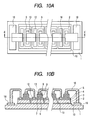
In the embodiment, the diodes comprising the protective circuit 22 were described as utilizing a pn junction across the base/collector of the HBT21. However, diodes utilizing a pn junction across the base/emitter may also be used. FIG. 9A shows a planar (flat) structure of the protective circuit 22 in that case. FIG. 9B shows a cross section structure taken along DD′ of FIG. 9A. The reference numerals, 1, 2, 3, 4, 5, 6, 7, 8, and 9 here respectively indicate the semi-insulating GaAs substrate, the n-type GaAs subcollector layer (Si concentration 5×1018 cm−3, film thickness 0.6 μm), the n-type GaAs collector layer (Si concentration 1×1018 cm−3, film thickness 1.0 μm), the p-type GaAs base layer (C concentration 4×1019 cm−3, film thickness 150 nm), the n-type InGaP emitter layer (InP mol ratio 0.5, Si concentration 3×1017 cm−3, film thickness 30 nm), the n-type GaAs layer (Si concentration 3×1017 cm−3, film thickness 90 nm), the n-type AlGaAs ballast resistance layer (AlAs mol ratio 0.33, Si concentration 1×1017 cm−3, film thickness 120 nm), the n-type GaAs contact layer (Si concentration 1×1018 cm−3, film thickness 50 nm), and an n-type InGaAs contact layer (InAs mol ratio 0.5, Si concentration 1×1018 cm−3, film thickness 50 nm). The reference numerals 12, 13, 16, and 18 respectively indicate a base electrode formed from layers of Ti (film thickness 50 nm), Pt (film thickness 50 nm), and Au (film thickness 200 nm), an emitter electrode formed from layers of WSi (Si mol ratio 0.3, film thickness 0.3 μm), the wiring connected serially with each diode, and the metallic pads for electrically connecting to the HBT. The reference numeral 10 indicates an isolation groove for electrically isolating each diode. In the example in the present embodiment, the HBT21 and the protective circuit 22 are connected by bonding wire however these components may be directly connected via the wiring 16.
In the present embodiment, the diodes comprising the protective circuit 22 switch electrically to the on state at the stage where approximately 1.2 volts are applied. Therefore, when for example utilizing a protective circuit 22 with ten diode stages connected in series, and twelve volts is applied across the collector/emitter of the HBT21, the protective circuit 22 switches to the on state to prevent the HBT21 from damage.
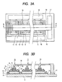
A plan view of another embodiment of the protective circuit 22 is shown in FIG. 10A. A cross section of the structure taken along lines EE′ of FIG. 10A is shown in FIG. 10B. The reference numerals, 1, 2, 3, 4, 5, 6, 7, 8, and 9 here respectively indicate the semi-insulating GaAs substrate, the n-type GaAs subcollector layer (Si concentration 5×1018 cm−3, film thickness 0.6 μm), the n-type GaAs collector layer (Si concentration 1×1018 cm−3, film thickness 1.0 μm), the p-type GaAs base layer (C concentration 4×1019 cm−3, film thickness 150 nm), the n-type InGaP emitter layer (InP mol ratio 0.5, Si concentration 3×1017 cm−3, film thickness 30 nm), the n-type GaAs layer (Si concentration 3×1017 cm−3, film thickness 90 nm), the n-type AlGaAs ballast resistance layer (AlAs mol ratio 0.33, Si concentration 1×1017 cm−3, film thickness 120 nm), the n-type GaAs contact layer (Si concentration 1×1019 cm−3, film thickness 50 nm), and an n-type InGaAs contact layer (InAs mol ratio 0.5, Si concentration 1×1019 cm−3, film thickness 50 nm). The reference numerals 12, 13, 16, and 18 respectively indicate a base electrode formed from layers of Ti (film thickness 50 nm), Pt (film thickness 50 nm), and Au (film thickness 200 nm), an emitter electrode formed from layers of WSi (Si mol ratio 0.3, film thickness 0.3 μm), the wiring connected serially with each diode, and the metallic pads for electrically connecting to the HBT. In the example in the present embodiment, the HBT21 and the protective circuit 22 are connected by bonding wire; however, these components may directly be connected via the wiring 16.
Fifth Embodiment
The power amplifier constituting the fifth embodiment of the present invention is described next while referring to the accompanying drawings. The present embodiment is for describing the fundamental principle of the present invention and shows a general or concept shape of each section. FIG. 11 is a block diagram of the power amplifier of the present embodiment. The present embodiment is a power amplifier with a two-stage structure. The reference numerals 24, 25 in the figure, are respectively the first amplifier circuit and the second amplifier circuit. The reference numerals 26 a, 26 b, 26 c are respectively the input matching circuit, the inter-stage matching circuit, and the output matching circuit. The amplified RF signal is input to the power amplifier from the terminal 27. After passing through the (impedance) matching circuits 26 a, 26 b, 26 c and being amplified in the amplifier circuits 24, 25, the signal is output from the terminal 28.
FIG. 12 and FIG. 13 are respectively a cross sectional drawing and planar (plan view) drawing showing the mounted state of a typical power amplifier module. A semiconductor device 51, and a passive element 52 are mounted on the substrate 60. The reference numeral 54 indicates a conductive layer for connecting electrical signals to the semiconductor device 51. In this example, the multiple substrates 60, 61, 62 are stacked in a layer. The semiconductor device 51 is the previously described power amplifier.
Circuit diagrams of the first amplifier 24, and the second amplifier 25 are respectively shown in FIG. 14 and FIG. 15. The first amplifier 24 circuit is comprised a multifinger HBT made up of 10 basic HBT connected in parallel and with an emitter size of 108 μm2. The second amplifier 25 circuit is comprised a multifinger HBT made up of 60 basic HBT connected in parallel and with an emitter size of 108 μm2.
The basic HBT is comprised of an n-type GaAs subcollector layer (Si concentration 5×1018 cm−3, film thickness 0.6 μm), an n-type GaAs collector layer (Si concentration 1×1018 cm−3, film thickness 1.0 μm), a p-type GaAs base layer (C concentration 4×1018 cm−3, film thickness 150 nm), an n-type InGaP emitter layer (InP mol ratio 0.5, Si concentration 3×1017 cm−3, film thickness 30 nm), an n-type GaAs layer (Si concentration 3×1017 cm−3, film thickness 90 nm), an n-type AlGaAs ballast resistance layer (AlAs mol ratio 0.33, Si concentration 1×1017 cm−3, film thickness 120 nm), an n-type GaAs contact layer (Si concentration 1×1018 cm−3, film thickness 50 nm), and an n-type InGaAs contact layer (InAs mol ratio 0.5, Si concentration 1×1018 cm−3, film thickness 50 nm) are formed on at least the semi-insulating GaAs substrate. In the example of the HBT shown in FIG. 14, and FIG. 15, the bases, emitters and collectors of the individual HBT are connected in parallel with each other.
The second amplifier circuit 25 may be the amplifier circuit as shown in the circuit diagram of FIG. 16. In other words, it may be a protective circuit for protecting the HBT21 from damage when an excessive voltage such as a static charge is applied to the HBT21. The protective circuit is connected in parallel across the emitter and collector of the HBT21. The protective circuit 22 is formed on a semi-insulating GaAs substrate identical to that of the HBT21.
Comparing Characteristics of the Present Invention with the Structure of the Related Art
Heterojunction bipolar transistors (or HBT) including the cross sectional structures shown in FIG. 18 and FIG. 19 were fabricated and a comparison made of their reliability order to quantitatively determine in the present invention, the importance in terms of reliability of inserting a GaAs layer between the InGaP emitter layer and the AlGaAs ballast resistance layer. FIG. 18 shows the structure of the HBT in WO98/53502 Table 1 (patent document 1). A laminated structure comprised of an n-type GaAs subcollector layer 2, an n-type GaAs collector layer 3, a p-type GaAs base layer 4, an n-type InGaP emitter layer 5, an n-type AlGaAs ballast resistance layer 7, an n-type GaAs contact layer 8, and an n-type InGaAs contact layer 9 are sequentially formed in layers on the semi-insulating GaAs substrate 1. The reference numerals 11, 12, 13 in FIG. 18 respectively denote the collector electrode, base electrode, and emitter electrode. For purposes of comparison, FIG. 19 shows a structure fabricated without the AlGaAs ballast resistance layer. The laminated structure is comprised of an n-type GaAs subcollector layer 2, an n-type GaAs collector layer 3, a p-type GaAs base layer 4, an n-type InGaP emitter layer 5, an n-type GaAs layer 20, an n-type GaAs contact layer 8, and an n-type InGaAs contact layer 9 sequentially formed in layers on the semi-insulating GaAs substrate 1. The reference numerals 11, 12, 13 in FIG. 2B respectively denote the collector electrode, base electrode, and emitter electrode.
Heterojunction bipolar transistors (or HBT) with the structures shown in FIG. 18 and FIG. 9 were subjected to an electrical conduction test under identical conditions where a collector current density of 40 kA/cm2, and a junction temperature of 210° C. were applied for 300 hours. Results of the test showed deterioration occurred in all twenty of the HBT with the structures shown in FIG. 18 containing an AlGaAs ballast resistance layer directly on the InGaP emitter layer. In contrast, there was no deterioration in the electrical conduction test, performed on the twenty comparison HBT shown in FIG. 19 not containing the AlGaAs ballast resistance layer.
In the results from comparing reliability, the reason for the short life of the HBT containing an AlGaAs ballast resistance layer directly on the InGaP emitter layer are as follows. A deep donor impurity level called a DX center exists within the AlGaAs layer and functions as a nonradiative (non-emissive) recombination center. Holes reverse-injected to the n-type InGaP emitter layer side from the p-type GaAs base layer reach the AlGaAs ballast resistance layer by diffusion. These holes that arrived by diffusion recombine as electrons via the DX center. Lattice defects increase with the energy emitted at this time, and reach a level causing deterioration in the device.

Claims (2)

1. A power amplifier including multiple stages of connected amplifier circuits comprised of at least one or more heterojunction bipolar transistors connected in parallel, wherein the heterojunction bipolar transistor is a sequentially formed structure comprised at least of an InGaP emitter layer and, a base layer forming a heterojunction together with the InGaP emitter layer on one side; and a low-doped GaAs layer and an AlGaAs ballast resistance layer on the other side, wherein the donor concentration of said low-doped GaAs layer is less than that of the AlGaAs ballast resistance layer.
2. The power amplifier according to claim 1, including a voltage limiter protection circuit connected electrically in parallel between the emitter and the collector.
US12/879,205 2004-01-19 2010-09-10 Heterojunction bipolar transistor and method for manufacturing the same, and power amplifier using the same Expired - Fee Related US8072001B2 (en)

Priority Applications (1)

Application Number Priority Date Filing Date Title
US12/879,205 US8072001B2 (en) 2004-01-19 2010-09-10 Heterojunction bipolar transistor and method for manufacturing the same, and power amplifier using the same

Applications Claiming Priority (7)

Application Number Priority Date Filing Date Title
JP2004010288 2004-01-19
JP2004-010288 2004-01-19
JP2004287312A JP4977313B2 (en) 2004-01-19 2004-09-30 Heterojunction bipolar transistor
JP2004-287312 2004-09-30
US11/019,270 US7256434B2 (en) 2004-01-19 2004-12-23 Heterojunction bipolar transistor and method for manufacturing the same, and power amplifier using the same
US11/723,769 US7804109B2 (en) 2004-01-19 2007-03-22 Heterojunction bipolar transistor and method for manufacturing the same, and power amplifier using the same
US12/879,205 US8072001B2 (en) 2004-01-19 2010-09-10 Heterojunction bipolar transistor and method for manufacturing the same, and power amplifier using the same

Related Parent Applications (1)

Application Number Title Priority Date Filing Date
US11/723,769 Division US7804109B2 (en) 2004-01-19 2007-03-22 Heterojunction bipolar transistor and method for manufacturing the same, and power amplifier using the same

Publications (2)

Publication Number Publication Date
US20100327980A1 US20100327980A1 (en) 2010-12-30
US8072001B2 true US8072001B2 (en) 2011-12-06

Family

ID=34752117

Family Applications (3)

Application Number Title Priority Date Filing Date
US11/019,270 Expired - Fee Related US7256434B2 (en) 2004-01-19 2004-12-23 Heterojunction bipolar transistor and method for manufacturing the same, and power amplifier using the same
US11/723,769 Active US7804109B2 (en) 2004-01-19 2007-03-22 Heterojunction bipolar transistor and method for manufacturing the same, and power amplifier using the same
US12/879,205 Expired - Fee Related US8072001B2 (en) 2004-01-19 2010-09-10 Heterojunction bipolar transistor and method for manufacturing the same, and power amplifier using the same

Family Applications Before (2)

Application Number Title Priority Date Filing Date
US11/019,270 Expired - Fee Related US7256434B2 (en) 2004-01-19 2004-12-23 Heterojunction bipolar transistor and method for manufacturing the same, and power amplifier using the same
US11/723,769 Active US7804109B2 (en) 2004-01-19 2007-03-22 Heterojunction bipolar transistor and method for manufacturing the same, and power amplifier using the same

Country Status (2)

Country Link
US (3) US7256434B2 (en)
JP (1) JP4977313B2 (en)

Cited By (1)

* Cited by examiner, † Cited by third party
Publication number Priority date Publication date Assignee Title
CN103872107A (en) * 2012-12-18 2014-06-18 株式会社村田制作所 Heterojunction bipolar transistor, power amplifier including the same, and method for fabricating heterojunction bipolar transistor

Families Citing this family (28)

* Cited by examiner, † Cited by third party
Publication number Priority date Publication date Assignee Title
JP4977313B2 (en) * 2004-01-19 2012-07-18 ルネサスエレクトロニクス株式会社 Heterojunction bipolar transistor
JP2006185990A (en) * 2004-12-27 2006-07-13 Renesas Technology Corp Semiconductor apparatus and its manufacturing method, and electronic device
JP5035588B2 (en) * 2005-11-21 2012-09-26 株式会社村田製作所 Semiconductor device having bipolar transistor
US8193609B2 (en) * 2008-05-15 2012-06-05 Triquint Semiconductor, Inc. Heterojunction bipolar transistor device with electrostatic discharge ruggedness
WO2010116700A1 (en) * 2009-04-07 2010-10-14 住友化学株式会社 Semiconductor substrate, manufacturing method therefor, and electronic device
CN105051873B (en) * 2013-03-19 2017-06-13 株式会社村田制作所 Heterojunction bipolar transistor
RU2556765C1 (en) * 2014-02-25 2015-07-20 Федеральное государственное бюджетное образовательное учреждение высшего профессионального образования Кабардино-Балкарский государственный университет им. Х.М. Бербекова Manufacturing method of semiconductor structure
US10109623B2 (en) 2014-05-08 2018-10-23 Qorvo Us, Inc. Dual-series varactor EPI
US20150325573A1 (en) 2014-05-08 2015-11-12 Triquint Semiconductor, Inc. Dual stack varactor
US9245837B1 (en) * 2014-07-07 2016-01-26 Infineon Technologies Ag Radio frequency power device
US9484471B2 (en) 2014-09-12 2016-11-01 Qorvo Us, Inc. Compound varactor
WO2016047217A1 (en) 2014-09-22 2016-03-31 株式会社村田製作所 Semiconductor device
WO2016113938A1 (en) * 2015-01-14 2016-07-21 三菱電機株式会社 Semiconductor device and method for manufacturing semiconductor device
JP6315300B2 (en) * 2015-02-17 2018-04-25 株式会社村田製作所 Heterojunction bipolar transistor
US9590669B2 (en) 2015-05-08 2017-03-07 Qorvo Us, Inc. Single varactor stack with low second-harmonic generation
CN105449004B (en) * 2015-12-17 2018-02-27 中国电子科技集团公司第五十五研究所 A kind of AlGaAs beam leads PIN diode and preparation method thereof
US9905678B2 (en) 2016-02-17 2018-02-27 Qorvo Us, Inc. Semiconductor device with multiple HBTs having different emitter ballast resistances
JP2017220584A (en) * 2016-06-08 2017-12-14 株式会社村田製作所 Semiconductor device and power amplifier circuit
US10109724B2 (en) * 2017-02-22 2018-10-23 Qualcomm Incorporated Heterojunction bipolar transistor unit cell and power stage for a power amplifier
JP2018142688A (en) * 2017-02-28 2018-09-13 株式会社村田製作所 Semiconductor device
CN108511411B (en) 2017-02-28 2021-09-10 株式会社村田制作所 Semiconductor device with a plurality of semiconductor chips
US11227862B2 (en) 2017-02-28 2022-01-18 Murata Manufacturing Co., Ltd. Semiconductor device
JP2018186144A (en) * 2017-04-25 2018-11-22 株式会社村田製作所 Semiconductor device and power amplifier module
US10580748B2 (en) 2017-12-06 2020-03-03 Murata Manufacturing Co., Ltd. Semiconductor apparatus
JP2020013926A (en) * 2018-07-19 2020-01-23 株式会社村田製作所 Semiconductor device
JP2020031191A (en) 2018-08-24 2020-02-27 株式会社村田製作所 Heterojunction bipolar transistor and semiconductor device
JP2020184580A (en) * 2019-05-08 2020-11-12 株式会社村田製作所 Semiconductor device
JP2021132100A (en) * 2020-02-19 2021-09-09 株式会社村田製作所 High-frequency power amplifier element

Citations (9)

* Cited by examiner, † Cited by third party
Publication number Priority date Publication date Assignee Title
JPH09102502A (en) 1995-10-06 1997-04-15 Fujitsu Ltd Hetero-junction-type bipolar transistor and its manufacturing method
WO1998053502A1 (en) 1997-05-22 1998-11-26 Mitsubishi Denki Kabushiki Kaisha Semiconductor device and method for manufacturing the same
JP2000260784A (en) 1999-03-12 2000-09-22 Sharp Corp Heterojunction bipolar transistor, semiconductor device using the same, and manufacture of the heterojunction bipolar transistor
US6507089B1 (en) 1999-06-16 2003-01-14 Nec Corporation Semiconductor device, semiconductor integrated circuit, and method for manufacturing semiconductor device
JP2003023012A (en) 2001-07-06 2003-01-24 Toshiba Corp Heterojunction bipolar transistor and manufacturing method therefor
US6545340B1 (en) * 1998-09-22 2003-04-08 Qinetiq Limited Semiconductor device
JP2004006531A (en) 2002-05-31 2004-01-08 Renesas Technology Corp Semiconductor device and its manufacturing method
US6768140B1 (en) 2002-04-03 2004-07-27 Skyworks Solutions, Inc. Structure and method in an HBT for an emitter ballast resistor with improved characteristics
US20050156194A1 (en) * 2004-01-19 2005-07-21 Isao Ohbu Heterojunction bipolar transistor and method for manufacturing the same, and power amplifier using the same

Family Cites Families (7)

* Cited by examiner, † Cited by third party
Publication number Priority date Publication date Assignee Title
JP3117831B2 (en) * 1993-02-17 2000-12-18 シャープ株式会社 Semiconductor device
JP3294461B2 (en) * 1995-03-14 2002-06-24 シャープ株式会社 Heterojunction bipolar transistor and manufacturing method thereof
FR2736468B1 (en) * 1995-07-07 1997-08-14 Thomson Csf BIPOLAR TRANSISTOR WITH OPTIMIZED STRUCTURE
JP3594482B2 (en) * 1998-04-02 2004-12-02 三菱電機株式会社 Heterojunction bipolar transistor
JP3429706B2 (en) * 1999-06-25 2003-07-22 シャープ株式会社 Heterojunction bipolar transistor and manufacturing method thereof
JP2001156078A (en) * 1999-11-29 2001-06-08 Nec Corp Hetero-junction bipolar transistor
JP2003007715A (en) * 2001-06-26 2003-01-10 Nippon Telegr & Teleph Corp <Ntt> Bipolar transistor

Patent Citations (14)

* Cited by examiner, † Cited by third party
Publication number Priority date Publication date Assignee Title
JPH09102502A (en) 1995-10-06 1997-04-15 Fujitsu Ltd Hetero-junction-type bipolar transistor and its manufacturing method
WO1998053502A1 (en) 1997-05-22 1998-11-26 Mitsubishi Denki Kabushiki Kaisha Semiconductor device and method for manufacturing the same
US6545340B1 (en) * 1998-09-22 2003-04-08 Qinetiq Limited Semiconductor device
US20020088993A1 (en) 1999-03-12 2002-07-11 Twynam John K. Heterojunction bipolar transistor capable of restraining the conductivity modulation of the ballast layer
JP2000260784A (en) 1999-03-12 2000-09-22 Sharp Corp Heterojunction bipolar transistor, semiconductor device using the same, and manufacture of the heterojunction bipolar transistor
US6611008B2 (en) 1999-03-12 2003-08-26 Sharp Kabushiki Kaisha Heterojunction bipolar transistor capable of restraining the conductivity modulation of the ballast layer
US6507089B1 (en) 1999-06-16 2003-01-14 Nec Corporation Semiconductor device, semiconductor integrated circuit, and method for manufacturing semiconductor device
JP2003023012A (en) 2001-07-06 2003-01-24 Toshiba Corp Heterojunction bipolar transistor and manufacturing method therefor
US6768140B1 (en) 2002-04-03 2004-07-27 Skyworks Solutions, Inc. Structure and method in an HBT for an emitter ballast resistor with improved characteristics
JP2004006531A (en) 2002-05-31 2004-01-08 Renesas Technology Corp Semiconductor device and its manufacturing method
US7045877B2 (en) * 2002-05-31 2006-05-16 Renesas Technology Corp. Semiconductor protection device
US20050156194A1 (en) * 2004-01-19 2005-07-21 Isao Ohbu Heterojunction bipolar transistor and method for manufacturing the same, and power amplifier using the same
US20070164316A1 (en) * 2004-01-19 2007-07-19 Renesas Technology Corp. Heterojunction bipolar transistor and method for manufacturing the same, and power amplifier using the same
US20100327980A1 (en) * 2004-01-19 2010-12-30 Renesas Electronics Corporation Heterojunction bipolar transistor and method for manufacturing the same, and power amplifier using the same

Cited By (2)

* Cited by examiner, † Cited by third party
Publication number Priority date Publication date Assignee Title
CN103872107A (en) * 2012-12-18 2014-06-18 株式会社村田制作所 Heterojunction bipolar transistor, power amplifier including the same, and method for fabricating heterojunction bipolar transistor
CN103872107B (en) * 2012-12-18 2017-05-17 株式会社村田制作所 Heterojunction bipolar transistor, power amplifier including the same, and method for fabricating heterojunction bipolar transistor

Also Published As

Publication number Publication date
JP2005236259A (en) 2005-09-02
US20100327980A1 (en) 2010-12-30
US7256434B2 (en) 2007-08-14
US20070164316A1 (en) 2007-07-19
JP4977313B2 (en) 2012-07-18
US7804109B2 (en) 2010-09-28
US20050156194A1 (en) 2005-07-21

Similar Documents

Publication Publication Date Title
US8072001B2 (en) Heterojunction bipolar transistor and method for manufacturing the same, and power amplifier using the same
US7176099B2 (en) Hetero-junction bipolar transistor and manufacturing method thereof
US6943387B2 (en) Semiconductor device, manufacturing thereof and power amplifier module
JP2007173624A (en) Hetero-junction bipolar transistor and method of manufacturing same
US20060138459A1 (en) Semiconductor device, manufacturing method of the same and electronic device
US7566920B2 (en) Bipolar transistor and power amplifier
US6696711B2 (en) Semiconductor device and power amplifier using the same
TW201818542A (en) Heterojunction bipolar transistor
US20060030113A1 (en) Heterojunction bipolar transistor and method for fabricating the same
TW201911525A (en) Semiconductor device
JP2005259755A (en) Hetero-junction bipolar transistor and its manufacturing method
US6881639B2 (en) Method of manufacturing semiconductor device
US5528189A (en) Noise performance of amplifiers
US20020195620A1 (en) Compound semiconductor device having heterojunction bipolar transister and other component integrated together and process for fabrication thereof
EP1497868A1 (en) Structure and method for an emitter ballast resistor in an hbt
JP5543936B2 (en) Method of manufacturing heterojunction bipolar transistor and power amplifier using heterojunction bipolar transistor
JP2010183054A (en) Heterojunction bipolar transistor and method of manufacturing the same
US7323728B2 (en) Semiconductor device
CN110858589A (en) Heterojunction bipolar transistor and semiconductor device
US6777301B2 (en) Method of producing hetero-junction bipolar transistor
JP4818985B2 (en) Heterojunction bipolar transistor
JP3221646B2 (en) Heterojunction bipolar transistor
JP2004111941A (en) Bipolar transistor and method of manufacturing the same
JP2007035809A (en) Semiconductor device and its manufacturing method
JP2015065294A (en) Semiconductor device and power amplifier

Legal Events

Date Code Title Description
STCF Information on status: patent grant

Free format text: PATENTED CASE

FEPP Fee payment procedure

Free format text: PAYOR NUMBER ASSIGNED (ORIGINAL EVENT CODE: ASPN); ENTITY STATUS OF PATENT OWNER: LARGE ENTITY

FPAY Fee payment

Year of fee payment: 4

AS Assignment

Owner name: RENESAS ELECTRONICS CORPORATION, JAPAN

Free format text: CHANGE OF ADDRESS;ASSIGNOR:RENESAS ELECTRONICS CORPORATION;REEL/FRAME:044928/0001

Effective date: 20150806

FEPP Fee payment procedure

Free format text: MAINTENANCE FEE REMINDER MAILED (ORIGINAL EVENT CODE: REM.); ENTITY STATUS OF PATENT OWNER: LARGE ENTITY

LAPS Lapse for failure to pay maintenance fees

Free format text: PATENT EXPIRED FOR FAILURE TO PAY MAINTENANCE FEES (ORIGINAL EVENT CODE: EXP.); ENTITY STATUS OF PATENT OWNER: LARGE ENTITY

STCH Information on status: patent discontinuation

Free format text: PATENT EXPIRED DUE TO NONPAYMENT OF MAINTENANCE FEES UNDER 37 CFR 1.362

FP Lapsed due to failure to pay maintenance fee

Effective date: 20191206