US8054383B2 - Display apparatus and method of preventing image burn-in - Google Patents
Display apparatus and method of preventing image burn-in Download PDFInfo
- Publication number
- US8054383B2 US8054383B2 US11/491,975 US49197506A US8054383B2 US 8054383 B2 US8054383 B2 US 8054383B2 US 49197506 A US49197506 A US 49197506A US 8054383 B2 US8054383 B2 US 8054383B2
- Authority
- US
- United States
- Prior art keywords
- data
- pixel
- osd
- osd data
- display
- Prior art date
- Legal status (The legal status is an assumption and is not a legal conclusion. Google has not performed a legal analysis and makes no representation as to the accuracy of the status listed.)
- Expired - Fee Related, expires
Links
Images


Classifications
-
- G—PHYSICS
- G09—EDUCATION; CRYPTOGRAPHY; DISPLAY; ADVERTISING; SEALS
- G09G—ARRANGEMENTS OR CIRCUITS FOR CONTROL OF INDICATING DEVICES USING STATIC MEANS TO PRESENT VARIABLE INFORMATION
- G09G3/00—Control arrangements or circuits, of interest only in connection with visual indicators other than cathode-ray tubes
- G09G3/20—Control arrangements or circuits, of interest only in connection with visual indicators other than cathode-ray tubes for presentation of an assembly of a number of characters, e.g. a page, by composing the assembly by combination of individual elements arranged in a matrix no fixed position being assigned to or needed to be assigned to the individual characters or partial characters
- G09G3/2007—Display of intermediate tones
-
- G—PHYSICS
- G09—EDUCATION; CRYPTOGRAPHY; DISPLAY; ADVERTISING; SEALS
- G09G—ARRANGEMENTS OR CIRCUITS FOR CONTROL OF INDICATING DEVICES USING STATIC MEANS TO PRESENT VARIABLE INFORMATION
- G09G3/00—Control arrangements or circuits, of interest only in connection with visual indicators other than cathode-ray tubes
- G09G3/007—Use of pixel shift techniques, e.g. by mechanical shift of the physical pixels or by optical shift of the perceived pixels
-
- G—PHYSICS
- G09—EDUCATION; CRYPTOGRAPHY; DISPLAY; ADVERTISING; SEALS
- G09G—ARRANGEMENTS OR CIRCUITS FOR CONTROL OF INDICATING DEVICES USING STATIC MEANS TO PRESENT VARIABLE INFORMATION
- G09G3/00—Control arrangements or circuits, of interest only in connection with visual indicators other than cathode-ray tubes
- G09G3/20—Control arrangements or circuits, of interest only in connection with visual indicators other than cathode-ray tubes for presentation of an assembly of a number of characters, e.g. a page, by composing the assembly by combination of individual elements arranged in a matrix no fixed position being assigned to or needed to be assigned to the individual characters or partial characters
- G09G3/22—Control arrangements or circuits, of interest only in connection with visual indicators other than cathode-ray tubes for presentation of an assembly of a number of characters, e.g. a page, by composing the assembly by combination of individual elements arranged in a matrix no fixed position being assigned to or needed to be assigned to the individual characters or partial characters using controlled light sources
- G09G3/28—Control arrangements or circuits, of interest only in connection with visual indicators other than cathode-ray tubes for presentation of an assembly of a number of characters, e.g. a page, by composing the assembly by combination of individual elements arranged in a matrix no fixed position being assigned to or needed to be assigned to the individual characters or partial characters using controlled light sources using luminous gas-discharge panels, e.g. plasma panels
- G09G3/288—Control arrangements or circuits, of interest only in connection with visual indicators other than cathode-ray tubes for presentation of an assembly of a number of characters, e.g. a page, by composing the assembly by combination of individual elements arranged in a matrix no fixed position being assigned to or needed to be assigned to the individual characters or partial characters using controlled light sources using luminous gas-discharge panels, e.g. plasma panels using AC panels
- G09G3/296—Driving circuits for producing the waveforms applied to the driving electrodes
-
- G—PHYSICS
- G09—EDUCATION; CRYPTOGRAPHY; DISPLAY; ADVERTISING; SEALS
- G09G—ARRANGEMENTS OR CIRCUITS FOR CONTROL OF INDICATING DEVICES USING STATIC MEANS TO PRESENT VARIABLE INFORMATION
- G09G3/00—Control arrangements or circuits, of interest only in connection with visual indicators other than cathode-ray tubes
- G09G3/20—Control arrangements or circuits, of interest only in connection with visual indicators other than cathode-ray tubes for presentation of an assembly of a number of characters, e.g. a page, by composing the assembly by combination of individual elements arranged in a matrix no fixed position being assigned to or needed to be assigned to the individual characters or partial characters
- G09G3/34—Control arrangements or circuits, of interest only in connection with visual indicators other than cathode-ray tubes for presentation of an assembly of a number of characters, e.g. a page, by composing the assembly by combination of individual elements arranged in a matrix no fixed position being assigned to or needed to be assigned to the individual characters or partial characters by control of light from an independent source
- G09G3/36—Control arrangements or circuits, of interest only in connection with visual indicators other than cathode-ray tubes for presentation of an assembly of a number of characters, e.g. a page, by composing the assembly by combination of individual elements arranged in a matrix no fixed position being assigned to or needed to be assigned to the individual characters or partial characters by control of light from an independent source using liquid crystals
-
- G—PHYSICS
- G09—EDUCATION; CRYPTOGRAPHY; DISPLAY; ADVERTISING; SEALS
- G09G—ARRANGEMENTS OR CIRCUITS FOR CONTROL OF INDICATING DEVICES USING STATIC MEANS TO PRESENT VARIABLE INFORMATION
- G09G2320/00—Control of display operating conditions
- G09G2320/04—Maintaining the quality of display appearance
- G09G2320/043—Preventing or counteracting the effects of ageing
- G09G2320/046—Dealing with screen burn-in prevention or compensation of the effects thereof
-
- G—PHYSICS
- G09—EDUCATION; CRYPTOGRAPHY; DISPLAY; ADVERTISING; SEALS
- G09G—ARRANGEMENTS OR CIRCUITS FOR CONTROL OF INDICATING DEVICES USING STATIC MEANS TO PRESENT VARIABLE INFORMATION
- G09G2330/00—Aspects of power supply; Aspects of display protection and defect management
- G09G2330/02—Details of power systems and of start or stop of display operation
- G09G2330/021—Power management, e.g. power saving
-
- G—PHYSICS
- G09—EDUCATION; CRYPTOGRAPHY; DISPLAY; ADVERTISING; SEALS
- G09G—ARRANGEMENTS OR CIRCUITS FOR CONTROL OF INDICATING DEVICES USING STATIC MEANS TO PRESENT VARIABLE INFORMATION
- G09G2340/00—Aspects of display data processing
- G09G2340/10—Mixing of images, i.e. displayed pixel being the result of an operation, e.g. adding, on the corresponding input pixels
-
- H—ELECTRICITY
- H04—ELECTRIC COMMUNICATION TECHNIQUE
- H04N—PICTORIAL COMMUNICATION, e.g. TELEVISION
- H04N5/00—Details of television systems
- H04N5/44—Receiver circuitry for the reception of television signals according to analogue transmission standards
- H04N5/445—Receiver circuitry for the reception of television signals according to analogue transmission standards for displaying additional information
Definitions
- the present general inventive concept relates to a display apparatus and a method of preventing image burn-in thereof, and more specifically, to a display apparatus which performs an eliminating operation of image burn-in using an OSD (on-screen display) function and a method of preventing the image burn-in thereof.
- OSD on-screen display
- a CRT Cathode Ray Tube
- the CRT has some problems in that it is heavy, thick, and consumes too much power.
- the CRT has been replaced with an FPD (Flat Panel Display).
- An LCD Liquid Crystal Display
- PDP Plasma Display Panel
- the PDP and LCD have a problem in that when still images are displayed for a long period of time thereon, image burn-in is induced by the still images.
- image burn-in is induced by the still images.
- the PDP if still images are displayed for a long period of time, phosphors in barrier ribs of cells become worn out, and thus image burn-in occurs between a bright side and a dark side of the PDP.
- the LCD a response to a video signal is not very rapid, and thus image burn-in of previous still images remains while the still images are replaced by other images. Image burn-in reduces an image quality of the PDP or LCD, which may give rise to complaints from consumers.
- the conventional methods which prevent image burn-in by shifting a screen, can prevent the image burn-in by a signal located on a border line.
- image burn-in cannot effectively be prevented with respect to the partial region.
- the conventional method of preventing the image burn-in using a sensor needs a separate sensor circuit, and may decrease brightness due to an operation recognition error of the sensor when a user does not approach the display apparatus.
- the present general inventive concept provides a display apparatus, which can effectively prevent image burn-in by generating and displaying OSD (on-screen display) data according to a data value of an input video signal, and a method of prevent the image burn-in thereof.
- OSD on-screen display
- a method of preventing image burn-in of a display apparatus which displays an image comprising detecting pixel data of a first pixel of the image, calculating OSD data corresponding to the detected pixel data, generating the calculated OSD data, and merging the OSD data with the pixel data and displaying the merged data in the first pixel for a predetermined refresh period of time.
- the method may further comprise sequentially shifting the OSD data from the first pixel to each of a plurality of pixels, and sequentially displaying the shifted OSD data in each of the plurality of pixels for the predetermined refresh period of time.
- the OSD data may be displayed in a predetermined size.
- the OSD data may be sequentially shifted in a predetermined direction by a pixel unit.
- the detecting of the pixel data of the image may comprise detecting R, G, and B data values of the first pixel.
- the calculating of the OSD data may comprise comparing a value of the detected pixel data to a predetermined reference value, deducting the predetermined value from the detected pixel data value if the detected pixel data value is greater than the reference value, and adding the predetermined value to the detected pixel data value if the detected pixel data value is smaller than the reference value.
- a method of preventing image burn-in of a display apparatus which displays an image comprising detecting R, G, and B data of a predetermined pixel of the image, comparing values of each of the detected R, G, and B data to a predetermined reference value to calculate OSD data values corresponding to each of the R, G, and B data values, and generating OSD data according to the calculated OSD data values, merging the OSD data with the R, G, and B data and displaying the merged data in the predetermined pixel for a predetermined refresh period of time.
- the method may further comprise sequentially shifting the OSD data in a predetermined direction by a pixel unit.
- a display apparatus having a display to display an image, comprising an OSD generator to generate OSD data corresponding to pixel data of a video signal, a signal processor to process the video signal, to merge the video signal with the OSD data, and to output the merged data to the display, and a controller to detect the pixel data, to control the OSD generator to generate the OSD data corresponding to the pixel data, and to control the OSD data to be sequentially shifted on the display.
- the controller may comprise a pixel detector to detect the pixel data, an OSD calculator to calculate an OSD data value corresponding to a value of the detected pixel data, and a shift executer to control the OSD data, which correspond to the calculated OSD data value, to be sequentially shifted and then displayed.
- the shift executer may control the OSD data to be sequentially shifted from a location of a predetermined pixel on the display.
- the shift executer may control the OSD data to be sequentially shifted in a predetermined size on the display.
- the shift executer may control the OSD data to be sequentially shifted in a predetermined direction by a pixel unit.
- a display apparatus having a display unit to display an image, comprising a processing unit to generate OSD data for each pixel of a plurality of pixels using corresponding image data of respective ones of the plurality of pixels and to merge the OSD data with the corresponding image data, and a control unit to control the processing unit to generate the OSD data and to merge the OSD data with the corresponding image data, and to control the display unit to sequentially display the merged data in the respective ones of the plurality of pixels for a predetermined period of time.
- the controller may calculate OSD data values using values of the corresponding image data, and may control the processing unit to generate the OSD data using the OSD data values.
- the controller may compare the values of the corresponding image data to a predetermined reference value, and may calculate the OSD data values based on the comparison results.
- a display device to display images, comprising a data managing unit to generate OSD data for each pixel of a plurality of groups of pixels using corresponding image data of each pixel and to merge the OSD data for each pixel with the corresponding image data, and a control unit to control the data managing unit to generate the OSD data and to merge the OSD data for each pixel with the corresponding image data, and to control the display device to sequentially display the merged data for each group of pixels of the plurality of groups of pixels for a predetermined period of time.
- a method to prevent image burn-in in an image forming apparatus comprising generating OSD data for each pixel of a plurality of pixels using corresponding image data of respective ones of the plurality of pixels, merging the OSD data with the corresponding image data, and sequentially displaying the merged data in the respective ones of the plurality of pixels for a predetermined period of time.
- the generating of the OSD data may comprise calculating OSD data values using values of the corresponding image data, and generating the OSD data using the OSD data values.
- the calculating of the OSD data values may comprise comparing the values of the corresponding image data to a predetermined reference value, and calculating the OSD data values based on the comparison results.
- a method to prevent image burn-in in an image forming apparatus comprising generating OSD data for each pixel of a plurality of groups of pixels using corresponding image data each pixels, merging the OSD data of each pixel with the corresponding image data, and sequentially display the merged data for each group of pixels of the plurality of groups of pixels for a predetermined period of time.
- FIG. 1 is a control block diagram illustrating a display apparatus, according to an embodiment of the present general inventive concept
- FIG. 2 is a view illustrating a control flow chart of the display apparatus of FIG. 1 , according to an embodiment of the present general inventive concept
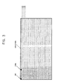
- FIG. 3 is a view illustrating a shifting method of a screen of a display apparatus, according to an embodiment of the present general inventive concept.
- FIG. 1 is a control block diagram illustrating a display apparatus, according to an embodiment of the present general inventive concept.
- a display apparatus can include a signal receiver 10 to receive a broadcast signal and a predetermined signal from an external source, a signal processor 20 to process the received signal, a display 30 to display the processed signal as an image, an OSD (on-screen display) generator 40 , and a controller 50 .
- a signal receiver 10 to receive a broadcast signal and a predetermined signal from an external source
- a signal processor 20 to process the received signal
- a display 30 to display the processed signal as an image
- an OSD (on-screen display) generator 40 to display the processed signal as an image
- an OSD on-screen display
- the signal receiver 10 includes an antenna 11 to receive the broadcast signal, and a tuner 12 to tune the broadcast signal of a specific channel selected by a user. Also, the signal receiver 10 may include a CVBS (Composite Video Baseband Signal) terminal 13 , an S-video terminal 14 , a Component terminal 15 , a PC-signal terminal 16 , a DVI (digital video/visual interactive) terminal 17 , and a HDMI (High-Definition Multimedia Interface) terminal 18 , in which a video signal corresponding to various external sources is received.
- CVBS Composite Video Baseband Signal
- S-video terminal 14 an S-video terminal 14
- Component terminal 15 Component terminal 15
- PC-signal terminal 16 Component terminal
- DVI digital video/visual interactive
- HDMI High-Definition Multimedia Interface
- the signal processor 20 transforms the signal input through the signal receiver 10 to a signal format which can be processed by the display 30 .
- the signal processor 20 may include a video decoder 21 , an A/D (analogue/digital) converter 22 , a TMDS receiver 23 , and a scaler 24 .
- the video decoder 21 decodes an analogue video signal, such as a CVBS (composite video broadcast signal) or an S-video signal, input from an analogue connection terminal and outputs the decoded signal to the scaler 24 .
- the A/D converter 22 transforms an input analogue video signal, such as a component signal or a PC signal, to a digital video signal and outputs the transformed signal to the scaler 24 .
- the TMDS receiver 23 splits a digital video signal, such as a DVI signal input from outside of the display apparatus through the signal receiver 10 , into an RGB digital signal and an HN synchronization signal and outputs the split signal to the scaler 24 .
- the scaler 24 transforms the input video signal such that the video signal has a vertical frequency, a resolution, a screen ratio, etc., fitted for an output standard of the display 30 .
- the display 30 receives the video signal from the signal processor 20 to display an image.
- the display 30 includes a display panel (see FIG. 3 ) on which an image is displayed, and a panel driver (not illustrated) to drive the display panel to display the image by processing the video signal input from the signal processor 20 .
- a display panel see FIG. 3
- a panel driver not illustrated
- an LCD panel or PDP panel can be used as an example of the display panel, the present general inventive concept is not so limited, and thus other display panels that have possibility of burn-in are also applicable.
- the OSD generator 40 generates OSD data for each pixel of the video signal according to a control signal of the controller 50 , which will be described later.
- a video signal output from the OSD generator 40 is mixed with the video signal output from the scaler 24 , and then displayed on the display panel of the display 30 .
- the controller 50 detects pixel data of the video signal processed by the scaler 24 , and controls the OSD generator 40 to generate the OSD data corresponding to the pixel data.
- the controller 50 can be implemented as a software program and a processor, such as a microcomputer, a CPU (central processing unit), etc., to load and execute the program.
- the controller 50 according to this embodiment of the present general inventive concept may include a pixel detector 51 , an OSD calculator 52 , and a shift executer 53 .
- the pixel detector 51 detects values of R (red), G (green), and B (blue) data, corresponding to each pixel of the video signal processed by the scaler 24 .
- the OSD calculator 52 calculates an OSD data value corresponding to each pixel based on the R, G, and B data values detected by the pixel detector 51 .
- the OSD data value calculated for each pixel by the OSD calculator 52 which may be programmed to have a predetermined difference from the R, G, and B data values, may be determined as a more effective value to prevent image burn-in according to the broadcast signal and the display apparatus.
- the value of 128 can be added or subtracted to/from each value of R, G and B data value to calculate as the OSD data value for that pixel.
- the OSD calculator 52 calculates an OSD data value for each of the R, G, and B data values, and calculates different OSD data values corresponding to the R, G, and B data values if the R, G, and B data values are different from one another. Needless to say, other values can be added/subtracted and such value may change during the calculation process (need not stay constant).
- the OSD generator 40 transforms the calculated OSD data value to the OSD data and outputs the OSD data to the scaler 24 , which in turn merges the R, G, and B data of a pixel with the corresponding OSD data for that pixel and outputs the merged OSD data to the display 30 .
- the merged OSD data can be set to a predetermined size and can be displayed in a predetermined number of pixels, for example in one pixel, as in this embodiment of the present general inventive concept. That is, the merged OSD data is displayed in one pixel of a screen displayed on the display 30 .
- One pixel is a very small pixel unit, and thus image burn-in can be prevented while at the same time a user does not detect a change in the screen even though the merged data is being displayed in the one pixel.
- the size of the OSD data can be varied so that a plurality of pixels can be constituted as the OSD data. In this case, plurality of OSD data values can be calculated and merged simultaneously to the corresponding number of image data values in the scaler.
- the shift executer 53 controls the OSD data such that the OSD data is sequentially shifted from a predetermined location on the screen of the display 30 in a predetermined direction to be displayed thereon. For example, the shift executer 53 detects R, G, and B data from an upper left end pixel of the screen, generates OSD data corresponding to the R, G, and B data, merges the OSD data with the corresponding R, G, and B data, and displays the merged OSD data in the upper left end pixel.
- the shift executer 53 allows the OSD data to be shifted to an adjacent pixel, adjacent to the right side of the upper left end pixel (i.e., a next pixel), to generate next OSD data corresponding to R, G, and B data of the next pixel, to merge the OSD data with the corresponding the R, G, and B data of the next pixel, and to display the OSD data on corresponding location, i.e., in the next pixel.
- the display apparatus is applied with power and an image is displayed on a screen thereof, it is possible to prevent image burn-in from occurring on the screen by generating and displaying OSD data of one or more pixel size and then sequentially shifting the OSD data one or more pixel at a time.
- OSD data has been described as shifting in a left-to-right linear direction, the present general inventive concept is not so limited.
- the OSD data may be shifted in any direction, such as vertically, horizontally, and/or diagonally, and may be shifted according to a predetermined pattern or randomly.
- the pixel detector 51 , the OSD calculator 52 , and the shift executer 53 may be implemented by an algorithm which can be programmed according to various known methods.
- FIG. 2 is a view illustrating a control flow chart of the display apparatus of FIG. 1 , according to an embodiment of the present general inventive concept.
- the pixel detector 51 sequentially detects R, G, and B image data for each pixel of a video signal, which is processed through the signal processor 20 , located on a left top side of the display panel (operation 100 ).
- the controller 50 determines whether a value of the detected R data is greater than a predetermined value, such as 128 (operation 101 ).
- the value of the detected R data value minus the predetermined value, such as 128, is set as an OSD data value (operation 102 ). If the detected R data value is smaller than the predetermined value, such as 128, then the value of detected R data value plus the predetermined value, such as 128, is set as the OSD data value (operation 103 ).
- the predetermined value is not required to be 128, and thus may alternatively be other values.
- the OSD generator 40 generates OSD data R′ corresponding to the calculated OSD data value for the detected R data value, and outputs the OSD data R′ to the scaler 24 (operation 104 ).
- the scaler 24 merges the OSD data R′ with detected R data to output the merged OSD (i.e., R′ and R) data to the display 30 , and the display 30 displays the merged OSD (i.e., R′ and R) data in a corresponding pixel (operation 105 ).
- the other image data for that pixel i.e., the detected G and B data and the corresponding OSD data G′ and B′ also are displayed in the corresponding pixel through the same process.
- Each of R′, G′, and B′ may comprise of values for a plurality of pixels.
- the merged OSD data continues to be displayed ( 106 ).
- the OSD data is shifted from the pixel to a next pixel, such as the pixel adjacent to the previous pixel (operation 107 ).
- OSD data is displayed on a pixel located on a left top side of a display panel for a predetermined refresh period of time.
- the OSD data is shifted to a next pixel adjacent to the previous pixel.
- the OSD data is sequentially shifted along the top line of pixels in the direction of (1) in FIG. 3 , and when the OSD data has been shifted to a pixel located on a right top side of the display channel, the OSD data is then shifted to a next line (i.e., from the top most line to a second line from the top), and then is shifted along the second line of pixels from the top in the direction of (2).
- the OSD data is shifted and proceeded along the third, fourth, etc., lines of pixels in the directions of (3), (4), etc., to cover all pixels of the display panel, and then the OSD data is returned to the original location to begin the shifting process again.
- the shifting of the OSD data is described as beginning at the top left pixel and proceeding from left to right and top to bottom, the present general inventive concept is not so limited. Accordingly, the shifting can begin at any pixel, and can proceed sequentially according to any predetermined pattern or can proceed randomly in the absence of a predetermined pattern.
- the OSD data having a value corresponding to R, G, and B data values of the original image data is shifted in pixel units (i.e., from one pixel to another) to be sequentially displayed in various pixels, and thus image burn-in can be prevented.
- the shifting of the pixel as described above may occur a plurality of pixels at a time without departing from the spirit or scope of the present invention.
- This process can be constantly performed during a power on state of the display apparatus, and a refresh time period per pixel of OSD data can be set up differently according to a type of display apparatus and programming.
- OSD data is sequentially shifted from a left topside of a display, the present general inventive concept is not so limited, and thus the OSD data can instead be shifted in random order by detecting any pixel data and generating corresponding OSD data.
- a display apparatus may include a user input unit to select an image burn-in prevention function described above, which may include a wireless remote controller to output an optical signal according to a control of a user and a optical signal receiver, which is provided in the display apparatus, to receive the optical signal from the wireless remote controller.
- the controller performs the corresponding image burn-in prevention function only if the image burn-in prevention function is selected at the user input unit.
- the present general inventive concept encompass shifting OSD data from one pixel to another, the present general inventive concept is not so limited.
- the merged data may be initially displayed on a first plurality of pixels for a predetermined period of time, and then shifted to and displayed on a second plurality of pixels for the second period of time. Because a pixel unit is small, the merged data can be displayed on a plurality of pixel units, provided that a number of the plurality of pixel units is sufficiently small such that a user does not detect a change in the screen even though the merged data is being displayed in the plurality of pixels.
- a display apparatus which can effectively prevent image burn-in by generating and displaying OSD data according to a data value of an input video signal, and a method of preventing image burn-in thereof are provided.
Landscapes
- Engineering & Computer Science (AREA)
- Physics & Mathematics (AREA)
- Computer Hardware Design (AREA)
- General Physics & Mathematics (AREA)
- Theoretical Computer Science (AREA)
- Chemical & Material Sciences (AREA)
- Crystallography & Structural Chemistry (AREA)
- Power Engineering (AREA)
- Plasma & Fusion (AREA)
- Control Of Indicators Other Than Cathode Ray Tubes (AREA)
- Controls And Circuits For Display Device (AREA)
Applications Claiming Priority (3)
| Application Number | Priority Date | Filing Date | Title |
|---|---|---|---|
| KR2005-80834 | 2005-08-31 | ||
| KR1020050080834A KR100721909B1 (ko) | 2005-08-31 | 2005-08-31 | 디스플레이장치 및 그 잔상제거방법 |
| KR10-2005-0080834 | 2005-08-31 |
Publications (2)
| Publication Number | Publication Date |
|---|---|
| US20070046815A1 US20070046815A1 (en) | 2007-03-01 |
| US8054383B2 true US8054383B2 (en) | 2011-11-08 |
Family
ID=37803535
Family Applications (1)
| Application Number | Title | Priority Date | Filing Date |
|---|---|---|---|
| US11/491,975 Expired - Fee Related US8054383B2 (en) | 2005-08-31 | 2006-07-25 | Display apparatus and method of preventing image burn-in |
Country Status (3)
| Country | Link |
|---|---|
| US (1) | US8054383B2 (zh) |
| KR (1) | KR100721909B1 (zh) |
| CN (1) | CN100518263C (zh) |
Cited By (6)
| Publication number | Priority date | Publication date | Assignee | Title |
|---|---|---|---|---|
| US20100134686A1 (en) * | 2008-12-01 | 2010-06-03 | Mstar Semiconductor, Inc. | Automatic OSD Adjusting Device and Method |
| US20100253612A1 (en) * | 2009-04-07 | 2010-10-07 | Sony Corporation | Dynamically established backlight for energy conservation in lcd |
| US20140198193A1 (en) * | 2011-08-24 | 2014-07-17 | Sony Corporation | Head mount display and display control method |
| US9842530B2 (en) | 2016-01-26 | 2017-12-12 | Sony Corporation | Dynamically established white balance in video display device based on ambient light |
| US10079000B2 (en) | 2015-08-12 | 2018-09-18 | Microsoft Technology Licensing, Llc | Reducing display degradation |
| US20190180679A1 (en) * | 2017-12-12 | 2019-06-13 | Google Llc | Display calibration to minimize image retention |
Families Citing this family (11)
| Publication number | Priority date | Publication date | Assignee | Title |
|---|---|---|---|---|
| KR101479781B1 (ko) * | 2008-07-22 | 2015-01-06 | 엘지전자 주식회사 | 영상표시기기 |
| JP2013044913A (ja) * | 2011-08-24 | 2013-03-04 | Sony Corp | 表示装置及び表示制御方法 |
| US9093015B2 (en) * | 2012-01-27 | 2015-07-28 | Samsung Electronics Co., Ltd. | Display apparatus, upgrade apparatus, control method thereof, and display system |
| JP2014215312A (ja) * | 2013-04-22 | 2014-11-17 | 株式会社東芝 | 光学素子および表示システム |
| JP2016045403A (ja) * | 2014-08-25 | 2016-04-04 | キヤノン株式会社 | 表示装置及びその制御方法 |
| KR102127970B1 (ko) * | 2014-11-03 | 2020-06-29 | 삼성전자주식회사 | 디스플레이 장치 및 그 제어 방법 |
| CN105930119B (zh) * | 2016-04-19 | 2019-06-04 | Oppo广东移动通信有限公司 | 一种智能终端的显示控制方法及装置 |
| KR20180020830A (ko) * | 2016-08-19 | 2018-02-28 | 삼성전자주식회사 | 비디오월 시스템 및 그 제어방법과, 디스플레이장치 |
| US10802585B2 (en) | 2018-07-12 | 2020-10-13 | Apple Inc. | Electronic devices with display operation based on eye activity |
| JP7059994B2 (ja) * | 2019-09-13 | 2022-04-26 | カシオ計算機株式会社 | 表示装置及び表示動作制御方法 |
| TWI732407B (zh) | 2019-12-31 | 2021-07-01 | 技嘉科技股份有限公司 | 電子裝置及顯示裝置的防烙印方法 |
Citations (6)
| Publication number | Priority date | Publication date | Assignee | Title |
|---|---|---|---|---|
| CN1484433A (zh) | 2002-09-17 | 2004-03-24 | Lg������ʽ���� | 显示系统和消除该显示系统中残余图像的方法 |
| KR20040091297A (ko) | 2003-04-21 | 2004-10-28 | 엘지전자 주식회사 | 투사형 영상 표시장치의 잔상 방지장치 및 그 방법 |
| US20050104874A1 (en) | 2003-11-17 | 2005-05-19 | Hyung-Il Koh | Display apparatus and method of eliminating afterimage thereof |
| US7102694B2 (en) * | 2001-07-11 | 2006-09-05 | Samsung Electronics Co., Ltd. | Apparatus and method for eliminating afterimage state |
| KR200426057Y1 (ko) | 2006-06-08 | 2006-09-19 | 주식회사 엠코 | 콘크리트 슬래브 난간지주 설치용 노출철근 파지식 하부연결구 |
| US7403194B2 (en) * | 2002-12-26 | 2008-07-22 | Samsung Electronics Co., Ltd. | Image displayer having function of automatically eliminating afterimage and a method thereof |
Family Cites Families (2)
| Publication number | Priority date | Publication date | Assignee | Title |
|---|---|---|---|---|
| KR20040103155A (ko) * | 2003-05-31 | 2004-12-08 | 주식회사 대우일렉트로닉스 | 피디피 잔상방지를 위한 영상 신호 처리방법 |
| KR100543870B1 (ko) * | 2004-01-14 | 2006-01-23 | 엘지전자 주식회사 | Pdp의 자동잔상제거방법 및 장치 |
-
2005
- 2005-08-31 KR KR1020050080834A patent/KR100721909B1/ko not_active IP Right Cessation
-
2006
- 2006-07-25 US US11/491,975 patent/US8054383B2/en not_active Expired - Fee Related
- 2006-08-30 CN CNB2006101288223A patent/CN100518263C/zh not_active Expired - Fee Related
Patent Citations (8)
| Publication number | Priority date | Publication date | Assignee | Title |
|---|---|---|---|---|
| US7102694B2 (en) * | 2001-07-11 | 2006-09-05 | Samsung Electronics Co., Ltd. | Apparatus and method for eliminating afterimage state |
| CN1484433A (zh) | 2002-09-17 | 2004-03-24 | Lg������ʽ���� | 显示系统和消除该显示系统中残余图像的方法 |
| KR20040026057A (ko) | 2002-09-17 | 2004-03-27 | 엘지전자 주식회사 | 영상표시기기의 화면잔상방지 장치 및 방법 |
| US7474356B2 (en) * | 2002-09-17 | 2009-01-06 | Lg Electronics Inc. | Display system and method of eliminating residual image in the same |
| US7403194B2 (en) * | 2002-12-26 | 2008-07-22 | Samsung Electronics Co., Ltd. | Image displayer having function of automatically eliminating afterimage and a method thereof |
| KR20040091297A (ko) | 2003-04-21 | 2004-10-28 | 엘지전자 주식회사 | 투사형 영상 표시장치의 잔상 방지장치 및 그 방법 |
| US20050104874A1 (en) | 2003-11-17 | 2005-05-19 | Hyung-Il Koh | Display apparatus and method of eliminating afterimage thereof |
| KR200426057Y1 (ko) | 2006-06-08 | 2006-09-19 | 주식회사 엠코 | 콘크리트 슬래브 난간지주 설치용 노출철근 파지식 하부연결구 |
Cited By (8)
| Publication number | Priority date | Publication date | Assignee | Title |
|---|---|---|---|---|
| US20100134686A1 (en) * | 2008-12-01 | 2010-06-03 | Mstar Semiconductor, Inc. | Automatic OSD Adjusting Device and Method |
| US8334928B2 (en) * | 2008-12-01 | 2012-12-18 | Mstar Semiconductor, Inc. | Automatic OSD adjusting device and method |
| US20100253612A1 (en) * | 2009-04-07 | 2010-10-07 | Sony Corporation | Dynamically established backlight for energy conservation in lcd |
| US20140198193A1 (en) * | 2011-08-24 | 2014-07-17 | Sony Corporation | Head mount display and display control method |
| US9813697B2 (en) * | 2011-08-24 | 2017-11-07 | Sony Corporation | Head mount display and display control method |
| US10079000B2 (en) | 2015-08-12 | 2018-09-18 | Microsoft Technology Licensing, Llc | Reducing display degradation |
| US9842530B2 (en) | 2016-01-26 | 2017-12-12 | Sony Corporation | Dynamically established white balance in video display device based on ambient light |
| US20190180679A1 (en) * | 2017-12-12 | 2019-06-13 | Google Llc | Display calibration to minimize image retention |
Also Published As
| Publication number | Publication date |
|---|---|
| CN100518263C (zh) | 2009-07-22 |
| KR20070025077A (ko) | 2007-03-08 |
| KR100721909B1 (ko) | 2007-05-28 |
| CN1925579A (zh) | 2007-03-07 |
| US20070046815A1 (en) | 2007-03-01 |
Similar Documents
| Publication | Publication Date | Title |
|---|---|---|
| US8054383B2 (en) | Display apparatus and method of preventing image burn-in | |
| US7525514B2 (en) | Plasma display apparatus | |
| KR20070025292A (ko) | 디스플레이장치 | |
| US20060114275A1 (en) | Display apparatus and control method thereof | |
| US20070285380A1 (en) | Display apparatus and control method thereof | |
| US8094194B2 (en) | Display apparatus and control method thereof | |
| US20040135768A1 (en) | Image displayer having function of automatically eliminating afterimage and a method thereof | |
| JP2007274070A (ja) | 映像信号処理装置、映像機器、及び、映像信号処理方法 | |
| KR100756584B1 (ko) | 디스플레이장치 및 그 잔상제거방법 | |
| US20060103644A1 (en) | Display apparatus and method for eliminating incidental image thereof | |
| JP5032350B2 (ja) | 画像処理装置 | |
| KR20080011026A (ko) | 영상처리장치 및 영상처리방법 | |
| US7583256B2 (en) | Display apparatus and control method thereof | |
| US7738004B2 (en) | Display apparatus to display a picture according to an input video signal and control method thereof | |
| KR101090067B1 (ko) | 영상처리장치 및 그 제어방법 | |
| KR100710083B1 (ko) | 디스플레이장치 및 그 제어방법 | |
| KR100784690B1 (ko) | 자동 샤프니스 제어 방법 | |
| KR20080034590A (ko) | 경계면 잔상 제거 기능을 구비한 영상기기 및 그 제어방법 | |
| KR20060013201A (ko) | Lcd 소비전력 절감장치 및 방법 | |
| KR20060009216A (ko) | 영상표시 시스템 및 그 제어방법 | |
| KR20080067214A (ko) | 디스플레이 장치의 잔상제거 방법 |
Legal Events
| Date | Code | Title | Description |
|---|---|---|---|
| AS | Assignment |
Owner name: SAMSUNG ELECTRONICS CO., LTD., KOREA, REPUBLIC OF Free format text: ASSIGNMENT OF ASSIGNORS INTEREST;ASSIGNOR:LEE, SUNG-TAE;REEL/FRAME:018129/0652 Effective date: 20060724 |
|
| STCF | Information on status: patent grant |
Free format text: PATENTED CASE |
|
| FEPP | Fee payment procedure |
Free format text: PAYOR NUMBER ASSIGNED (ORIGINAL EVENT CODE: ASPN); ENTITY STATUS OF PATENT OWNER: LARGE ENTITY |
|
| FPAY | Fee payment |
Year of fee payment: 4 |
|
| FEPP | Fee payment procedure |
Free format text: MAINTENANCE FEE REMINDER MAILED (ORIGINAL EVENT CODE: REM.); ENTITY STATUS OF PATENT OWNER: LARGE ENTITY |
|
| LAPS | Lapse for failure to pay maintenance fees |
Free format text: PATENT EXPIRED FOR FAILURE TO PAY MAINTENANCE FEES (ORIGINAL EVENT CODE: EXP.); ENTITY STATUS OF PATENT OWNER: LARGE ENTITY |
|
| STCH | Information on status: patent discontinuation |
Free format text: PATENT EXPIRED DUE TO NONPAYMENT OF MAINTENANCE FEES UNDER 37 CFR 1.362 |
|
| FP | Lapsed due to failure to pay maintenance fee |
Effective date: 20191108 |