US8043953B2 - Semiconductor device including an LSI chip and a method for manufacturing the same - Google Patents
Semiconductor device including an LSI chip and a method for manufacturing the same Download PDFInfo
- Publication number
- US8043953B2 US8043953B2 US12/521,936 US52193608A US8043953B2 US 8043953 B2 US8043953 B2 US 8043953B2 US 52193608 A US52193608 A US 52193608A US 8043953 B2 US8043953 B2 US 8043953B2
- Authority
- US
- United States
- Prior art keywords
- externally connected
- connected pad
- insulating layer
- layer
- semiconductor device
- Prior art date
- Legal status (The legal status is an assumption and is not a legal conclusion. Google has not performed a legal analysis and makes no representation as to the accuracy of the status listed.)
- Expired - Fee Related, expires
Links
Images


Classifications
-
- H—ELECTRICITY
- H10—SEMICONDUCTOR DEVICES; ELECTRIC SOLID-STATE DEVICES NOT OTHERWISE PROVIDED FOR
- H10W—GENERIC PACKAGES, INTERCONNECTIONS, CONNECTORS OR OTHER CONSTRUCTIONAL DETAILS OF DEVICES COVERED BY CLASS H10
- H10W70/00—Package substrates; Interposers; Redistribution layers [RDL]
- H10W70/01—Manufacture or treatment
- H10W70/05—Manufacture or treatment of insulating or insulated package substrates, or of interposers, or of redistribution layers
- H10W70/08—Manufacture or treatment of insulating or insulated package substrates, or of interposers, or of redistribution layers by depositing layers on the chip or wafer, e.g. "chip-first" RDLs
- H10W70/09—Manufacture or treatment of insulating or insulated package substrates, or of interposers, or of redistribution layers by depositing layers on the chip or wafer, e.g. "chip-first" RDLs extending onto an encapsulation that laterally surrounds the chip or wafer, e.g. fan-out wafer level package [FOWLP] RDLs
-
- B—PERFORMING OPERATIONS; TRANSPORTING
- B23—MACHINE TOOLS; METAL-WORKING NOT OTHERWISE PROVIDED FOR
- B23K—SOLDERING OR UNSOLDERING; WELDING; CLADDING OR PLATING BY SOLDERING OR WELDING; CUTTING BY APPLYING HEAT LOCALLY, e.g. FLAME CUTTING; WORKING BY LASER BEAM
- B23K26/00—Working by laser beam, e.g. welding, cutting or boring
- B23K26/36—Removing material
- B23K26/38—Removing material by boring or cutting
- B23K26/382—Removing material by boring or cutting by boring
- B23K26/389—Removing material by boring or cutting by boring of fluid openings, e.g. nozzles, jets
-
- H—ELECTRICITY
- H10—SEMICONDUCTOR DEVICES; ELECTRIC SOLID-STATE DEVICES NOT OTHERWISE PROVIDED FOR
- H10W—GENERIC PACKAGES, INTERCONNECTIONS, CONNECTORS OR OTHER CONSTRUCTIONAL DETAILS OF DEVICES COVERED BY CLASS H10
- H10W20/00—Interconnections in chips, wafers or substrates
- H10W20/01—Manufacture or treatment
- H10W20/071—Manufacture or treatment of dielectric parts thereof
- H10W20/081—Manufacture or treatment of dielectric parts thereof by forming openings in the dielectric parts
-
- H—ELECTRICITY
- H10—SEMICONDUCTOR DEVICES; ELECTRIC SOLID-STATE DEVICES NOT OTHERWISE PROVIDED FOR
- H10W—GENERIC PACKAGES, INTERCONNECTIONS, CONNECTORS OR OTHER CONSTRUCTIONAL DETAILS OF DEVICES COVERED BY CLASS H10
- H10W70/00—Package substrates; Interposers; Redistribution layers [RDL]
- H10W70/099—Connecting interconnections to insulating or insulated package substrates, interposers or redistribution layers
-
- H—ELECTRICITY
- H10—SEMICONDUCTOR DEVICES; ELECTRIC SOLID-STATE DEVICES NOT OTHERWISE PROVIDED FOR
- H10W—GENERIC PACKAGES, INTERCONNECTIONS, CONNECTORS OR OTHER CONSTRUCTIONAL DETAILS OF DEVICES COVERED BY CLASS H10
- H10W70/00—Package substrates; Interposers; Redistribution layers [RDL]
- H10W70/60—Insulating or insulated package substrates; Interposers; Redistribution layers
- H10W70/611—Insulating or insulated package substrates; Interposers; Redistribution layers for connecting multiple chips together
- H10W70/614—Insulating or insulated package substrates; Interposers; Redistribution layers for connecting multiple chips together the multiple chips being integrally enclosed
-
- H—ELECTRICITY
- H10—SEMICONDUCTOR DEVICES; ELECTRIC SOLID-STATE DEVICES NOT OTHERWISE PROVIDED FOR
- H10W—GENERIC PACKAGES, INTERCONNECTIONS, CONNECTORS OR OTHER CONSTRUCTIONAL DETAILS OF DEVICES COVERED BY CLASS H10
- H10W70/00—Package substrates; Interposers; Redistribution layers [RDL]
- H10W70/60—Insulating or insulated package substrates; Interposers; Redistribution layers
- H10W70/67—Insulating or insulated package substrates; Interposers; Redistribution layers characterised by their insulating layers or insulating parts
- H10W70/68—Shapes or dispositions thereof
- H10W70/682—Shapes or dispositions thereof comprising holes having chips therein
-
- H—ELECTRICITY
- H10—SEMICONDUCTOR DEVICES; ELECTRIC SOLID-STATE DEVICES NOT OTHERWISE PROVIDED FOR
- H10W—GENERIC PACKAGES, INTERCONNECTIONS, CONNECTORS OR OTHER CONSTRUCTIONAL DETAILS OF DEVICES COVERED BY CLASS H10
- H10W70/00—Package substrates; Interposers; Redistribution layers [RDL]
- H10W70/60—Insulating or insulated package substrates; Interposers; Redistribution layers
- H10W70/67—Insulating or insulated package substrates; Interposers; Redistribution layers characterised by their insulating layers or insulating parts
- H10W70/68—Shapes or dispositions thereof
- H10W70/685—Shapes or dispositions thereof comprising multiple insulating layers
-
- H—ELECTRICITY
- H10—SEMICONDUCTOR DEVICES; ELECTRIC SOLID-STATE DEVICES NOT OTHERWISE PROVIDED FOR
- H10W—GENERIC PACKAGES, INTERCONNECTIONS, CONNECTORS OR OTHER CONSTRUCTIONAL DETAILS OF DEVICES COVERED BY CLASS H10
- H10W72/00—Interconnections or connectors in packages
- H10W72/01—Manufacture or treatment
- H10W72/012—Manufacture or treatment of bump connectors, dummy bumps or thermal bumps
- H10W72/01221—Manufacture or treatment of bump connectors, dummy bumps or thermal bumps using local deposition
- H10W72/01225—Manufacture or treatment of bump connectors, dummy bumps or thermal bumps using local deposition in solid form, e.g. by using a powder or by stud bumping
-
- H—ELECTRICITY
- H10—SEMICONDUCTOR DEVICES; ELECTRIC SOLID-STATE DEVICES NOT OTHERWISE PROVIDED FOR
- H10W—GENERIC PACKAGES, INTERCONNECTIONS, CONNECTORS OR OTHER CONSTRUCTIONAL DETAILS OF DEVICES COVERED BY CLASS H10
- H10W72/00—Interconnections or connectors in packages
- H10W72/071—Connecting or disconnecting
- H10W72/073—Connecting or disconnecting of die-attach connectors
-
- H—ELECTRICITY
- H10—SEMICONDUCTOR DEVICES; ELECTRIC SOLID-STATE DEVICES NOT OTHERWISE PROVIDED FOR
- H10W—GENERIC PACKAGES, INTERCONNECTIONS, CONNECTORS OR OTHER CONSTRUCTIONAL DETAILS OF DEVICES COVERED BY CLASS H10
- H10W72/00—Interconnections or connectors in packages
- H10W72/20—Bump connectors, e.g. solder bumps or copper pillars; Dummy bumps; Thermal bumps
- H10W72/251—Materials
-
- H—ELECTRICITY
- H10—SEMICONDUCTOR DEVICES; ELECTRIC SOLID-STATE DEVICES NOT OTHERWISE PROVIDED FOR
- H10W—GENERIC PACKAGES, INTERCONNECTIONS, CONNECTORS OR OTHER CONSTRUCTIONAL DETAILS OF DEVICES COVERED BY CLASS H10
- H10W72/00—Interconnections or connectors in packages
- H10W72/20—Bump connectors, e.g. solder bumps or copper pillars; Dummy bumps; Thermal bumps
- H10W72/29—Bond pads specially adapted therefor
-
- H—ELECTRICITY
- H10—SEMICONDUCTOR DEVICES; ELECTRIC SOLID-STATE DEVICES NOT OTHERWISE PROVIDED FOR
- H10W—GENERIC PACKAGES, INTERCONNECTIONS, CONNECTORS OR OTHER CONSTRUCTIONAL DETAILS OF DEVICES COVERED BY CLASS H10
- H10W72/00—Interconnections or connectors in packages
- H10W72/851—Dispositions of multiple connectors or interconnections
- H10W72/874—On different surfaces
-
- H—ELECTRICITY
- H10—SEMICONDUCTOR DEVICES; ELECTRIC SOLID-STATE DEVICES NOT OTHERWISE PROVIDED FOR
- H10W—GENERIC PACKAGES, INTERCONNECTIONS, CONNECTORS OR OTHER CONSTRUCTIONAL DETAILS OF DEVICES COVERED BY CLASS H10
- H10W72/00—Interconnections or connectors in packages
- H10W72/90—Bond pads, in general
- H10W72/941—Dispositions of bond pads
- H10W72/9413—Dispositions of bond pads on encapsulations
-
- H—ELECTRICITY
- H10—SEMICONDUCTOR DEVICES; ELECTRIC SOLID-STATE DEVICES NOT OTHERWISE PROVIDED FOR
- H10W—GENERIC PACKAGES, INTERCONNECTIONS, CONNECTORS OR OTHER CONSTRUCTIONAL DETAILS OF DEVICES COVERED BY CLASS H10
- H10W90/00—Package configurations
-
- H—ELECTRICITY
- H10—SEMICONDUCTOR DEVICES; ELECTRIC SOLID-STATE DEVICES NOT OTHERWISE PROVIDED FOR
- H10W—GENERIC PACKAGES, INTERCONNECTIONS, CONNECTORS OR OTHER CONSTRUCTIONAL DETAILS OF DEVICES COVERED BY CLASS H10
- H10W90/00—Package configurations
- H10W90/701—Package configurations characterised by the relative positions of pads or connectors relative to package parts
- H10W90/731—Package configurations characterised by the relative positions of pads or connectors relative to package parts of die-attach connectors
- H10W90/734—Package configurations characterised by the relative positions of pads or connectors relative to package parts of die-attach connectors between a chip and a stacked insulating package substrate, interposer or RDL
Definitions
- the present invention relates to a semiconductor device including an LSI chip and a method for manufacturing the same, and particularly to a semiconductor device that is readily manufactured, provides a high yield, and excels in reliability, and a method for manufacturing the same.
- a semiconductor device called a “substrate with a built-in chip” in which a individually divided LSI chip and the like are buried in a substrate made of resin and the like and a semiconductor device in which an insulating resin layer and a wiring layer are formed on an LSI chip.
- semiconductor devices such as a substrate with a built-in chip, it is necessary to bury a chip in a substrate made of resin and the like, then laminate an insulating layer over the substrate, and further form a via hole through the insulating layer to electrically connect an electrode pad on the chip to an external electric terminal and the like.
- An example of a method for forming a via hole through an insulating layer includes a method for forming an insulating layer made of a photosensitive resin on a substrate with a built-in chip, exposing the photosensitive resin to light, and developing the photosensitive resin to form a via hole.
- the mechanical strength of a photosensitive resin is, however, typically so low that the device is often disadvantageously unreliable.
- many sheet-shaped resin materials used to form the insulating layer are nonphotosensitive resins. Since photosensitive resins are not produced in volume, the use of a photosensitive resin disadvantageously increases the cost.
- nonphotosensitive resins are frequently used as sheet-shaped insulating materials used in printed wiring boards and the like. Nonphotosensitive resins are therefore produced in volume, and the use of a nonphotosensitive resin can reduce the cost.
- a nonphotosensitive resin is used to form an insulating layer in a semiconductor device with a built-in chip, however, there is a problem of how to form a via hole.
- a via hole is typically formed by using a laser beam.
- a laser beam passes through the insulating layer made of a nonphotosensitive resin, and an electrode pad located under the insulating layer and made of Al and the like is flied apart by irradiation of the laser beam.
- the device including a semiconductor chip is disadvantageously damaged.
- transition layer (A) is provided as a laser stopper layer.
- the transition layer is comprised of at least two metal layers ( 33 , 36 , and 37 ) and larger than die pad ( 24 ) of IC chip ( 20 ), which is a semiconductor element.
- the technology described in Japanese Patent Laid-Open No. 2003-7896 thus allows a laser beam to form a via hole without damage to the die pad (paragraph number (0009)).
- stud bump 105 is formed on electrode pad 104 on chip 101 , and insulating layer 109 made of epoxy and the like is laminated over the stud bump. A laser machining is then performed to form via hole 110 that reaches the stud bump ( FIG. 7 ).
- electrode pad 104 will not be directly irradiated with the laser beam. Therefore, the electrode pad is not flied apart by the laser beam, or the device including a semiconductor chip is not damaged (paragraph numbers (0022) and (0062)).
- the formation of the protective pattern described in Japanese Patent Laid-Open No. 2003-7896 involves resist application or attachment, resist patterning, wet processing for removing the resist, and other steps.
- the steps are therefore complicated, disadvantageously resulting in increase in cost.
- the material cost the resist material, chemicals for the wet processing, and the like disadvantageously add extra cost.
- the transition layer needs to be larger than the die pad (electrode pad)
- the inter-pad distance preliminarily needs to have a little large margin in consideration of the large transition layer, resulting in occurrence of problem in which number of pads is insufficient in the whole semiconductor device.
- the method described in Japanese Patent Laid-Open No. 2005-332887 does not require the resist patterning and the like, but an extra step of forming a stud bump. Since the stud bump has a certain height, the resin layer needs to be thicker than the stud bump, that is, the minimum resin thickness needs to be equal to or greater than the height of the stud bump. This imposes a structural constraint on the thickness of the insulating layer, which needs to be greater than the height of the bump. The method is unsuitable for mobile apparatus and other applications in which the semiconductor device is preferably as thin as possible. Further, the stud bump, which is typically circular, needs to cover the pad (which may not be circular) in the underlying layer in order to block the laser beam, disadvantageously resulting in occurrence of problem in which number of pads is insufficient in the whole semiconductor device.
- Japanese Patent Laid-Open No. 2003-7896 and Japanese Patent Laid-Open No. 2005-332887 relate to a printed wiring technology, and it is therefore difficult to apply them as they are to a substrate with a built-in chip, which completely differs in the size of wiring, the form of the entire substrate, and the like.
- An object of the present invention is to provide a semiconductor device that can be readily manufactured, can include a large number of pads, and can be thin, and a method for manufacturing the same.
- a typical aspect of the present invention relates to a semiconductor device, comprising:
- an insulating layer provided on the LSI chip and made of a nonphotosensitive resin, the insulating layer including a via hole in a position corresponding to the externally connected pad;
- the via hole is formed by irradiating the insulating layer with laser light.
- Another typical aspect of the present invention relates to a method for manufacturing a semiconductor device, comprising:
- Another typical aspect of the present invention relates to a method for manufacturing a semiconductor device, comprising:
- FIG. 1 is a cross-sectional view of an example of a semiconductor device of the present invention
- FIG. 2 includes cross-sectional views showing part of the semiconductor device of the present invention
- FIG. 3 shows an example of a method for manufacturing a semiconductor device according to the present invention
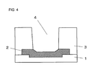
- FIG. 4 shows another example of the method for manufacturing a semiconductor device according to the present invention
- FIG. 5 shows another example of the method for manufacturing a semiconductor device according to the present invention
- FIG. 6 explains a semiconductor device of relate art
- FIG. 7 explains a semiconductor device of relate art.
- FIG. 1 is a cross-sectional view of an example of a semiconductor device of the present invention.
- the semiconductor device of the present invention comprises insulating layer 3 including via hole 4 formed in the position on individually divided LSI chip 1 including externally connected pad 2 that corresponds to the pad.
- Wiring layer 5 extending along insulating layer 3 through via hole 4 to externally connected pad 2 and electrically connected thereto, is formed.
- the insulating layer is made of a nonphotosensitive resin, and at least part of the via hole is directly formed above the externally connected pad by laser light irradiation.
- the structure in which at least part of the via hole is directly formed above the externally connected pad by laser light irradiation allows the semiconductor device of the present invention to be readily manufactured, provided with a large number of pads, and operated in a stable manner. Also, at least part of the via hole is formed above the externally connected pad by laser light irradiation. Directly forming at least part of the via hole above the externally connected pad this way without providing a laser stopper layer allows the steps to be simplified. Further, providing no laser stopper layer eliminates the need to address misalignment between the externally connected pad and the laser stopper layer and the like. A plurality of externally connected pads can therefore be provided at short spacings, whereby the number of externally connected pads on the chip can be maximized.
- All the via holes are preferably formed only by laser irradiation.
- the laser irradiation conditions are adjusted in accordance with the material of the insulating layer so that the via holes are formed to be deep enough to reach the respective externally connected pad, that is, to expose the externally connected pads, but the externally connected pads are not damaged by the laser irradiation. Forming the via holes by laser irradiation to be deep enough to reach the respective externally connected pads allows the advantageous effects described above to be more effectively achieved.
- LSIs are formed all at once on a wafer, and the “LSI chips” of the present invention are obtained, for example, by dicing the thus formed LSIs into individually divided ones.
- the externally connected pads are also preferably formed all at once on the wafer before the dicing.
- the material of the insulating layer is not limited to a specific one but may be any nonphotosensitive resin.
- the material is, however, preferably an epoxy resin, which is a thermoset resin, or a polyimide resin, which excels in heat resistance.
- Other examples of the material of the insulating layer include a liquid crystal polymer, a cardo resin, polyolefin, polyacrylate, polyamide, and a variety of other resin materials.
- the resin material may be comprised of only a resin.
- Another preferable resin material may also contain a variety of organic or inorganic fillers, glass cloth, alamido fibers, or other suitable fibrous reinforcing members.
- the preferable thickness of insulating layer can be selected as appropriate in consideration of electric characteristics such as the insulating property, characteristic impedance, and mechanical characteristics such as crack occurrence in a reliability test.
- the insulating layer may be a monolayer or a multilayer.
- the thickness of an insulating monolayer or an insulating multilayer preferably ranges from 1 ⁇ m to 500 ⁇ m inclusive, more preferably from 5 ⁇ m to 200 ⁇ m inclusive, still more preferably from 10 ⁇ m to 50 ⁇ m.
- the “externally connected pad” in the present invention is a pad for electrically connecting the LSI fabricated in the vicinity of the surface of the LSI chip to external components, and electrically connected to any of a power source, a ground line, a signal line, and other components.
- the cross-sectional diameter of the externally connected pad depends on the size of the LSI chip and the number of terminals to be connected and typically ranges from several micrometers to several hundred micrometers inclusive. For example, the diameter can be on the order of several ten micrometers.
- the cross-sectional shape of the externally connected pad can be a circle, an ellipse, an octagon, a rectangle, or other polygonal shapes.
- the cross-sectional diameter of each of the via holes depends on the size of the corresponding externally connected pad and the distance to the adjacent externally connected pad, and typically ranges from several micrometers to several hundred micrometers inclusive. That is, when the size of the pad or the distance to the adjacent pad is small, the size of the via hole tends to decrease and ranges from several micrometers to several ten micrometers. On the other hand, when the size of the pad or the distance to the adjacent pad is large, the size of the via hole tends to increase and ranges from several ten micrometers to several hundred micrometers.
- the cross-sectional shape of the via hole is typically a circle, but can be a shape close to an ellipse or a polygon. Since the via hole has a function of connecting to the wiring in an underlying layer, the depth of the via hole is equal to the thickness of the insulating layer or substantially equal to the thickness of the insulating layer from which the thickness of wiring in the underlying layer is subtracted.
- Examples of the laser used for the via hole formation may include an Nd-YAG laser, a CO 2 laser, and an excimer laser.
- a via hole formed above a chip is smaller than a via hole used in a printed wiring board in many cases.
- a CO 2 laser is preferably used to form a large via hole.
- the “position on the insulating layer that corresponds to the externally connected pad” means that the position of the externally connected pad coincides with (corresponds to; is aligned with) the position of the via hole, and it is particularly important that the bottom of the via hole is aligned with the pad. If the bottom of the via hole is misaligned with the pad, the laser beam directly damages the layer under the pad, resulting in destruction of the LSI wiring, the semiconductor element, and the like in the underlying layer.
- the wiring connected to the externally connected pad through the via hole may be monolayer or multilayer wiring.
- a resin layer may further be formed on the top layer to cover at least part of the wiring.
- the wiring layer is preferably made of Cu.
- the thickness of the wiring can be selected as appropriate in consideration of electric characteristics such as characteristic impedance and mechanical characteristics such as disconnection occurrence in a reliability test. Specifically, the thickness of the wiring preferably ranges from 0.1 ⁇ m to 100 ⁇ m inclusive, more preferably from 1 ⁇ m to 50 ⁇ m inclusive, still more preferably from 5 ⁇ m to 20 ⁇ m inclusive.
- the LSI chip is typically mounted on a substrate, and the LSI chip is electrically connected to the wiring above the substrate via the externally connected pad and the wiring layer extending from inside the via hole onto the insulating layer.
- the substrate on which the LSI chip is mounted forms a “substrate with a built-in chip.”
- the substrate on which the LSI chip is mounted is made of an epoxy resin, a BT resin, a phenol resin, or any other suitable resin impregnated with reinforcing material such as a glass-epoxy resin or core material, a layered prepreg impregnated with an epoxy resin, and the like or any other material typically used in a printed wiring board.
- Other examples may include a double-sided copper-clad laminate, a single-sided sheet, a resin sheet without a metal film, and a resin film as the substrate.
- the externally connected pad of the semiconductor device according to the present invention preferably includes the same surface as a reference surface of the LSI chip. Alternatively, the entire or part of the externally connected pad may be located on the LSI chip side under the reference surface of the LSI chip ( FIG. 2 ).
- the reference surface of the LSI chip used in the present invention means the final surface (front surface) of the LSI chip formed in an LSI front-end step.
- the reference surface of the LSI chip means the upper surface of a global wiring layer, which is the final metal layer formed in the front-end step, or the upper surface of an insulating layer (excluding the insulating layer made of a nonphotosensitive resin in which a via hole is formed according to the present invention) formed on the global wiring layer and made of silicon oxide, silicon nitride, and the like. That is, the reference surface is the surface where the LSI chip comes into contact with the insulating layer made of a nonphotosensitive resin and formed with a via hole thereon.
- the “LSI chip side” corresponds to the Si wafer side away from the reference surface (opposite the insulating layer made of a nonphotosensitive resin and formed with a via hole thereon). That is, in this case, part of the externally connected pad includes the same surface as the reference surface of the LSI chip, or the entire or part of the externally connected pad is located under the reference surface (on the Si wafer side, on the LSI chip side, or on the side opposite the insulating layer made of a nonphotosensitive resin and formed with a via hole thereon). “The entire externally connected pad is located under the reference surface” means that the externally connected pad is located completely under the reference surface.
- FIG. 2 shows examples of the externally connected pad.
- the via hole, the insulating layer, the wiring layer, and the like are omitted.
- FIG. 2( a ) shows a case where the upper surface of the externally connected pad coincides with (includes the same surface as) reference surface 7 of the LSI chip.
- FIG. 2( b ) shows a case where the entire externally connected pad is located on the LSI chip side under reference surface 7 of the LSI chip.
- FIG. 2( c ) shows a case where part of the externally connected pad is located on the LSI chip side under reference surface 7 of the LSI chip.
- the externally connected pad is formed by the front-end step.
- the externally connected pad is therefore formed on a surface planarized in a damascene step or any other suitable step, advantageously resulting in excellent flatness, stable via hole formation in the via hole machining step using laser irradiation, and highly reliable connection.
- the externally connected pad preferably includes a layer primarily containing Al.
- the layer primarily containing Al is a layer the Al content of which is at least 50% in terms of atomic ratio.
- Al—Si, Al—Cu, Al—Si—Cu, and other aluminum alloys can be used as well as Al alone. Using the alloys described above advantageously have better electromigration resistance and corrosion resistance than Al alone.
- the externally connected pad primarily containing Al is highly conformable to LSI manufacturing steps, whereby the yield of the semiconductor device can be high.
- the externally connected pad may be comprised of only a layer primarily containing Al or a layer primarily containing Al combined with other layers.
- the melting point of Al is approximately 660° C., which is approximately only one-half the melting points of Cu and the like. Therefore, when Al is simply irradiated with a laser beam, Al will be flied apart. The laser irradiation therefore needs to be carried out under the conditions in which Al is will not be flied apart.
- the externally connected pad may alternatively include a layer primarily containing Cu.
- the layer primarily containing Cu is a layer the Cu content of which is at least 50% in terms of atomic ratio.
- Cu is used as a wiring forming material in the front-end step and readily formed in the processes in the front-end step.
- the externally connected pad primarily containing Cu is highly conformable to LSI manufacturing steps, whereby the yield of the semiconductor device can be high.
- the externally connected pad may be comprised of only a layer primarily containing Cu or a layer primarily containing Cu combined with other layers.
- the externally connected pad is preferably a wire bonding pad (preferably also serves as a wire bonding pad).
- the cross-sectional size and shape of the externally connected pad preferably suit wire bonding.
- An example of the cross-sectional size and shape suitable for wire bonding may be a rectangle the short side or long side of which is approximately 100 ⁇ m in length. For example, such rectangles may be regularly arranged around the chip. Normal wire bonding connection or wiring connection after forming via holes can be used in a single LSI chip by using the externally connected pads as wire bonding pad.
- the externally connected pad also allows wire bonding connection as described above, the same chip can satisfy the following demands: wire bonding connection and wiring connection after via holes are formed, resulting in increase in consumption and cost reduction. Further, laser light irradiation increases the thickness of a surface oxide layer, advantageously resulting in improvement in desmear resistance and the like of the Al layer.
- the thickness of the externally connected pad can have a variety of values. It is, however, preferable that the externally connected pad has a certain thickness in consideration of damage due to laser light, preferably at least 1.0 ⁇ m. When the thickness of the pad is smaller than 1.0 ⁇ m, laser light may damage the externally connected pad. Further, to use the externally connected pad as a wire bonding pad, the externally connected pad needs to be thick enough to withstand wire bonding operation. In consideration of this as well as the reason described above, the thickness is preferably at least 1.0 ⁇ m. When the externally connected pad is at least 1.0 ⁇ m in thickness, the damage to the underlying semiconductor element and other components due to laser light can be reduced and suppressed. The resultant higher laser light irradiation energy acceptance level prevents the semiconductor element, the wiring, and the like from being damaged, whereby the semiconductor device has excellent reliability.
- the externally connected pad is comprised of a layer primarily containing Al
- the externally connected pad is often fabricated by combining sputtering and dry etching.
- the thickness of the externally connected pad is preferably 10 ⁇ m or smaller, more preferably 5 ⁇ m or smaller.
- the lower limit of the thickness is preferably at least 1.0 ⁇ m in order to provide stable electric characteristics.
- the externally connected pad is comprised of a layer primarily containing Cu
- the externally connected pad is formed also by sputtering and dry etching processes as part of the semiconductor front-end step or by using apparatus similar to those used in the front-end step.
- the thickness of the externally connected pad is preferably 10 ⁇ m or smaller, more preferably 5 ⁇ m or smaller.
- the lower limit of the thickness is preferably at least 1.0 ⁇ m, as in the case of Al.
- the thickness may be at least 0.5 ⁇ m in some cases.
- the thickness can be approximately 0.5 ⁇ m.
- the nonphotosensitive resin that forms the insulating layer preferably has a 95% decomposition temperature lower than the melting point of the material that forms the externally connected pad.
- the reaction in which a nonphotosensitive resin decomposes is an endothermic reaction, and the heat of decomposition is probably transferred from the surrounding system during the decomposition. Therefore, when the 95% decomposition temperature is lower than or equal to the melting point of the material that forms the externally connected pad, the material will not probably deform due to the heat. Further, the damage to the underlying layer is reduced because the temperature of the via hole portion will not rise in the temperature in which the nonphotosensitive resin decomposes. As a result, the semiconductor device can provide stable connection and high reliability.
- the melting point thereof is approximately 660° C., and it is preferable that at least 95% of the nonphotosensitive resin decomposes at a temperature lower than or equal to the melting point.
- the nonphotosensitive resin contains inorganic fillers (such as fibrous reinforcing members) made of silica and the like, the 95% decomposition temperature is determined by calculating whether or not 95% of the resin component excluding the inorganic fillers has decomposed. The 95% decomposition temperature of the nonphotosensitive resin is measured in compliance with the JIS K7120 method.
- the 95% decomposition temperature is defined by preparing a predetermined amount (approximately 10 mg) of a nonphotosensitive resin, and measuring the reduction in mass thereof when subjected to heat by using a thermobalance to find the point where the mass decreases by 95%.
- a first method for manufacturing a semiconductor device according to the present invention includes the following steps:
- FIG. 3 shows an example of the first method for manufacturing a semiconductor device.
- individually divided LSI chip 1 including externally connected pad 2 is prepared (step (1)).
- the LSI chip including the externally connected pad can be prepared by forming outermost-layer wiring (global wiring) of the LSI and then forming the externally connected pad made of Al and the like, for example, by using sputtering.
- the externally connected pad may be formed after a protective layer made of a resin and the like was formed in advance.
- the externally connected pad may be formed by stacking a plurality of conductive materials, such as Al and TiN.
- Insulating layer 3 made of a nonphotosensitive resin is then formed on LSI chip 1 (step (2), FIG. 3( a )). Thereafter, insulating layer 3 above externally connected pad 2 is irradiated with laser light, at position corresponding to externally connected pad 2 , to remove insulating layer 3 so as to form via hole 4 passing through insulating layer 3 to the depth that allows externally connected pad 2 to be exposed (step (3), FIG. 3( b )).
- FIG. 4 is an enlarged view showing a portion in the vicinity of via hole 4 thus formed above externally connected pad 2 .
- wiring layer 5 extending along insulating layer 3 through via hole 4 to externally connected pad 2 and electrically connected thereto is formed (step (4), FIG. 3( c )).
- a laser stopper layer comprised of a stud bump
- the steps can be simplified.
- a method for forming a via hole in the position in alignment with the externally connected pad by laser light irradiation can readily form a via hole, the following wiring formation can be readily carried out, and the pads can be provided at a high density.
- the insulating layer made of a nonphotosensitive resin is formed on the LSI chip in the step (2).
- This step can be carried out not only by forming a nonphotosensitive resin layer on an upwardly oriented active surface (LSI element surface) of the LSI chip but also by mounting the LSI chip with the active surface thereof downwardly oriented on a nonphotosensitive resin that has been prepared in advance.
- “Passing through the insulating layer to the depth that allows the externally connected pad to be exposed” in the step (3) described above means that the via hole is formed in such a way that the via hole is deep enough to reach externally connected pad 2 , that is, the via hole is open on externally connected pad 2 (the opening of the via hole exposes externally connected pad 2 to the outside).
- the intensity and the amount of irradiation of the laser light used for via hole formation are controlled in the step (3) described above in such a way that the via hole is formed to the depth that allows the externally connected pad to be exposed. In this way, the damage to the externally connected pad due to the laser light becomes very small.
- the width and thickness of the wiring and the like in an underlying layer of an LSI and the like are smaller than those of the wiring formed on or in a printed wiring board by one or two magnitudes or even smaller.
- a second method for manufacturing a semiconductor device according to the present invention includes the following steps:
- (C) a step of irradiating a position on the insulating layer corresponding to the is externally connected pad with laser light, to form an opening in the insulating layer in such a way that part of the insulating layer is left in the position corresponding to the externally connected pad; (D) a step of carrying out dry etching or wet etching at bottom of the opening, to remove the insulating layer left in the position corresponding to the externally connected pad, and then to form a via hole passing through the insulating layer so that the externally connected pad is exposed (E) a step of forming a wiring layer extending along the insulating layer through the via hole to the externally connected pad.
- FIG. 5 shows an example of the second method for manufacturing a semiconductor device.
- the steps (A) and (B) are carried out in the same manner as the steps (1) and (2) in the first method for manufacturing a semiconductor device.
- step (C) laser light irradiation is carried out in such a way that nonphotosensitive resin 6 is left on at least part of the bottom of the via hole (Laser light irradiation is carried out in such a way that nonphotosensitive resin 6 is left in the position on the insulating layer that corresponds to the externally connected pad, FIG. 5( a )). Thereafter, dry etching or wet etching is carried out against remaining nonphotosensitive resin 6 to remove resin 6 left on the bottom of the via hole (step (D), FIG. 5( b )).
- the resin is left on the bottom of the via hole, the laser energy is not directly transferred to the externally connected pad, whereby the damage to the underlying layer can be suppressed.
- the laser irradiation for via hole formation can be minimized. That is, to prevent the wiring and the like under the externally connected pad from being damaged, the laser light irradiation is stopped to leave the nonphotosensitive resin on the bottom of the via hole, and the slightly left nonphotosensitive resin is removed by dry etching, wet etching, or any other moderate method that does not greatly affect the LSI wiring or the underlying layer.
- dry etching may include ashing using O 2 , N 2 , Ar, CF 4 , and the like, IBE (Ion Beam Etching), and RIE (Reactive Ion Etching).
- IBE Ion Beam Etching
- RIE Reactive Ion Etching
- the prepared externally connected pad preferably includes an Al layer primarily containing Al and a TiN layer provided as an overlying layer on the Al layer.
- the material primarily containing Al is a material the Al content of which is at least 50% in terms of atomic ratio.
- Al—Si, Al—Cu, Al—Si—Cu, and other aluminum alloys can be used as well as Al alone.
- the laser light irradiation in the step (C) is carried out in such a way that part of the insulating layer and the entire TiN layer are left.
- dry etching is preferably carried out to remove the remaining insulating layer and TiN layer so that the Al layer of the externally connected pad is exposed.
- the externally connected pad comprised of the Al layer primarily containing Al can be protected from the damage during the via hole formation.
- the damage to the layer under the externally connected pad due to the laser irradiation can be reduced by stopping the laser irradiation in a state in which the TiN layer leaves.
- desmearing and other processes can be readily carried out by leaving the TiN layer, which is resistant to a desmearing solution, on the Al, which is less resistant to the desmearing solution.
- a via hole is formed by carrying out dry etching to open the remaining insulating layer and TiN layer, and then the externally connected pad can be electrically connected to external wiring.
- the method described above can provide a semiconductor device with excellent reliability at a high yield.
- the TiN layer can be formed as part of a typical semiconductor front-end step or a similar sputtering step.
- the semiconductor device of the present invention can be used as a device in which a chip used in a mobile phone, an electric apparatus, and the like is built in a substrate.
Landscapes
- Physics & Mathematics (AREA)
- Optics & Photonics (AREA)
- Engineering & Computer Science (AREA)
- Plasma & Fusion (AREA)
- Mechanical Engineering (AREA)
- Internal Circuitry In Semiconductor Integrated Circuit Devices (AREA)
- Design And Manufacture Of Integrated Circuits (AREA)
- Production Of Multi-Layered Print Wiring Board (AREA)
Abstract
Description
- 1: LSI chip
- 2: externally connected pad
- 3: nonphotosensitive resin
- 4: via hole
- 5: wiring layer
- 6: remaining insulating layer
(4) a step of forming a wiring layer extending along the insulating layer through the via hole to the externally connected pad.
(D) a step of carrying out dry etching or wet etching at bottom of the opening, to remove the insulating layer left in the position corresponding to the externally connected pad, and then to form a via hole passing through the insulating layer so that the externally connected pad is exposed
(E) a step of forming a wiring layer extending along the insulating layer through the via hole to the externally connected pad.
Claims (7)
Applications Claiming Priority (3)
| Application Number | Priority Date | Filing Date | Title |
|---|---|---|---|
| JP2007-018141 | 2007-01-29 | ||
| JP2007018141 | 2007-01-29 | ||
| PCT/JP2008/050343 WO2008093531A1 (en) | 2007-01-29 | 2008-01-15 | Semiconductor device and method for manufacturing the same |
Publications (2)
| Publication Number | Publication Date |
|---|---|
| US20090294951A1 US20090294951A1 (en) | 2009-12-03 |
| US8043953B2 true US8043953B2 (en) | 2011-10-25 |
Family
ID=39673845
Family Applications (1)
| Application Number | Title | Priority Date | Filing Date |
|---|---|---|---|
| US12/521,936 Expired - Fee Related US8043953B2 (en) | 2007-01-29 | 2008-01-15 | Semiconductor device including an LSI chip and a method for manufacturing the same |
Country Status (3)
| Country | Link |
|---|---|
| US (1) | US8043953B2 (en) |
| JP (1) | JPWO2008093531A1 (en) |
| WO (1) | WO2008093531A1 (en) |
Cited By (1)
| Publication number | Priority date | Publication date | Assignee | Title |
|---|---|---|---|---|
| US20120153507A1 (en) * | 2010-12-21 | 2012-06-21 | Shinko Electric Industries Co., Ltd. | Semiconductor device and method for manufacturing the same |
Families Citing this family (6)
| Publication number | Priority date | Publication date | Assignee | Title |
|---|---|---|---|---|
| JP2012074581A (en) * | 2010-09-29 | 2012-04-12 | Teramikros Inc | Semiconductor device and method for manufacturing the same |
| US8624342B2 (en) | 2010-11-05 | 2014-01-07 | Invensas Corporation | Rear-face illuminated solid state image sensors |
| KR102268385B1 (en) * | 2014-08-14 | 2021-06-23 | 삼성전기주식회사 | Printed circuit board and method of manufacturing the same |
| US10854550B2 (en) | 2017-09-28 | 2020-12-01 | Advanced Semiconductor Engineering, Inc. | Semiconductor package and method of manufacturing the same |
| KR102570902B1 (en) * | 2018-11-23 | 2023-08-25 | 삼성전자주식회사 | Semiconductor package |
| CN112366177B (en) * | 2020-11-10 | 2022-11-29 | 长江存储科技有限责任公司 | Semiconductor device and method of forming the same |
Citations (12)
| Publication number | Priority date | Publication date | Assignee | Title |
|---|---|---|---|---|
| JP2001094264A (en) | 1999-09-22 | 2001-04-06 | Ibiden Co Ltd | Multilayer printed wiring board and manufacturing method |
| US20010004134A1 (en) * | 1999-12-15 | 2001-06-21 | Kazuto Saitoh | Electronic device and method of producing same |
| US20010038145A1 (en) * | 2000-05-08 | 2001-11-08 | Naohiro Mashino | Multilayer wiring board, semiconductor device and methods for manufacturing such multilayer wiring board and semiconductor device |
| JP2002246504A (en) | 2000-12-15 | 2002-08-30 | Ibiden Co Ltd | Method for manufacturing multilayer printed wiring board incorporating semiconductor element |
| JP2003007896A (en) | 2001-06-26 | 2003-01-10 | Ibiden Co Ltd | Multilayer printed wiring board |
| US20040014317A1 (en) | 2000-09-25 | 2004-01-22 | Hajime Sakamoto | Semiconductor element, method of manufacturing semiconductor element, multi-layer printed circuit board, and method of manufacturing multi-layer printed circuit board |
| JP2004087991A (en) | 2002-08-28 | 2004-03-18 | Kyocera Corp | Method for manufacturing multilayer wiring board |
| JP2004165277A (en) | 2002-11-11 | 2004-06-10 | Shinko Electric Ind Co Ltd | Electronic component mounting structure and method of manufacturing the same |
| JP2005332887A (en) | 2004-05-18 | 2005-12-02 | Shinko Electric Ind Co Ltd | Method for forming multilayer wiring and method for manufacturing multilayer wiring board |
| US20080017925A1 (en) * | 2006-07-19 | 2008-01-24 | Semiconductor Energy Laboratory Co., Ltd. | Micro electro mechanical device and manufacturing method thereof |
| US20080083830A1 (en) * | 2006-04-28 | 2008-04-10 | Semiconductor Energy Laboratory Co., Ltd. | Memory device and semiconductor device |
| USRE41369E1 (en) * | 2002-12-24 | 2010-06-08 | Casio Computer Co., Ltd. | Semiconductor device and method of manufacturing the same |
Family Cites Families (7)
| Publication number | Priority date | Publication date | Assignee | Title |
|---|---|---|---|---|
| JP2004335641A (en) * | 2003-05-06 | 2004-11-25 | Canon Inc | Manufacturing method of semiconductor device embedded substrate |
| JP4414712B2 (en) * | 2003-09-29 | 2010-02-10 | 大日本印刷株式会社 | Manufacturing method of electronic device |
| JP2005217372A (en) * | 2004-02-02 | 2005-08-11 | Sony Corp | Substrate with built-in electronic components, substrate and manufacturing method thereof |
| JP4298559B2 (en) * | 2004-03-29 | 2009-07-22 | 新光電気工業株式会社 | Electronic component mounting structure and manufacturing method thereof |
| JP4268560B2 (en) * | 2004-04-27 | 2009-05-27 | 大日本印刷株式会社 | Electronic component built-in module and manufacturing method thereof |
| JP4431747B2 (en) * | 2004-10-22 | 2010-03-17 | 富士通株式会社 | Manufacturing method of semiconductor device |
| JP4759981B2 (en) * | 2004-11-02 | 2011-08-31 | 大日本印刷株式会社 | Manufacturing method of electronic component built-in module |
-
2008
- 2008-01-15 WO PCT/JP2008/050343 patent/WO2008093531A1/en not_active Ceased
- 2008-01-15 US US12/521,936 patent/US8043953B2/en not_active Expired - Fee Related
- 2008-01-15 JP JP2008556041A patent/JPWO2008093531A1/en active Pending
Patent Citations (14)
| Publication number | Priority date | Publication date | Assignee | Title |
|---|---|---|---|---|
| JP2001094264A (en) | 1999-09-22 | 2001-04-06 | Ibiden Co Ltd | Multilayer printed wiring board and manufacturing method |
| US20010004134A1 (en) * | 1999-12-15 | 2001-06-21 | Kazuto Saitoh | Electronic device and method of producing same |
| US20010038145A1 (en) * | 2000-05-08 | 2001-11-08 | Naohiro Mashino | Multilayer wiring board, semiconductor device and methods for manufacturing such multilayer wiring board and semiconductor device |
| US20040014317A1 (en) | 2000-09-25 | 2004-01-22 | Hajime Sakamoto | Semiconductor element, method of manufacturing semiconductor element, multi-layer printed circuit board, and method of manufacturing multi-layer printed circuit board |
| JP2002246504A (en) | 2000-12-15 | 2002-08-30 | Ibiden Co Ltd | Method for manufacturing multilayer printed wiring board incorporating semiconductor element |
| JP2003007896A (en) | 2001-06-26 | 2003-01-10 | Ibiden Co Ltd | Multilayer printed wiring board |
| JP2004087991A (en) | 2002-08-28 | 2004-03-18 | Kyocera Corp | Method for manufacturing multilayer wiring board |
| JP2004165277A (en) | 2002-11-11 | 2004-06-10 | Shinko Electric Ind Co Ltd | Electronic component mounting structure and method of manufacturing the same |
| US20040130013A1 (en) | 2002-11-11 | 2004-07-08 | Masahiro Sunohara | Electronic parts packaging structure and method of manufacturing the same |
| US20050042801A1 (en) | 2002-11-11 | 2005-02-24 | Shinko Electric Industries Co., Ltd. | Electronic parts packaging structure and method of manufacturing the same |
| USRE41369E1 (en) * | 2002-12-24 | 2010-06-08 | Casio Computer Co., Ltd. | Semiconductor device and method of manufacturing the same |
| JP2005332887A (en) | 2004-05-18 | 2005-12-02 | Shinko Electric Ind Co Ltd | Method for forming multilayer wiring and method for manufacturing multilayer wiring board |
| US20080083830A1 (en) * | 2006-04-28 | 2008-04-10 | Semiconductor Energy Laboratory Co., Ltd. | Memory device and semiconductor device |
| US20080017925A1 (en) * | 2006-07-19 | 2008-01-24 | Semiconductor Energy Laboratory Co., Ltd. | Micro electro mechanical device and manufacturing method thereof |
Cited By (1)
| Publication number | Priority date | Publication date | Assignee | Title |
|---|---|---|---|---|
| US20120153507A1 (en) * | 2010-12-21 | 2012-06-21 | Shinko Electric Industries Co., Ltd. | Semiconductor device and method for manufacturing the same |
Also Published As
| Publication number | Publication date |
|---|---|
| US20090294951A1 (en) | 2009-12-03 |
| JPWO2008093531A1 (en) | 2010-05-20 |
| WO2008093531A1 (en) | 2008-08-07 |
Similar Documents
| Publication | Publication Date | Title |
|---|---|---|
| US8043953B2 (en) | Semiconductor device including an LSI chip and a method for manufacturing the same | |
| JP5263918B2 (en) | Semiconductor device and manufacturing method thereof | |
| KR101319808B1 (en) | Method of manufacturing rigid-flexible printed circuit board | |
| US6580036B2 (en) | Multi-layer printed circuit board and a BGA semiconductor package using the multi-layer printed circuit board | |
| US8946906B2 (en) | Multilayer wiring substrate and method of manufacturing the same | |
| KR101015704B1 (en) | Chip embedded printed circuit board and its manufacturing method | |
| US8319115B2 (en) | Wiring board and manufacturing method thereof | |
| TW201014480A (en) | Wiring board with built-in electronic component and method for manufacturing the same | |
| KR20070058349A (en) | Semiconductor device and manufacturing method thereof, and semiconductor wafer | |
| JP5362569B2 (en) | Interposer and method of manufacturing interposer | |
| JP4441325B2 (en) | Method for forming multilayer wiring and method for manufacturing multilayer wiring board | |
| US8129835B2 (en) | Package substrate having semiconductor component embedded therein and fabrication method thereof | |
| US20140251657A1 (en) | Printed circuit board and method of manufacturing the same | |
| US20060219429A1 (en) | Multilayer wiring board and its manufacturing method | |
| JPWO2009101904A1 (en) | Semiconductor device and manufacturing method thereof | |
| TWI389275B (en) | Intermediate substrate and intermediate substrate manufacturing method | |
| KR101840305B1 (en) | Interposer for semiconductor package and method of manufacturing the same | |
| JP4063240B2 (en) | Semiconductor device mounting substrate, manufacturing method thereof, and semiconductor package | |
| CN103596354A (en) | Composite circuit boards with built-in spacers, interposers, and build-up circuits | |
| KR101501902B1 (en) | Printed circuit board substrate having metal post and the method of manufacturing the same | |
| KR102333097B1 (en) | Printed circuit board and method of manufacturing the same, and electronic component module | |
| JP2022015759A (en) | Method for manufacturing wiring board | |
| US20240047321A1 (en) | Integrated fan-out package and method of making same | |
| KR101148601B1 (en) | IC Module and Method of Manufacturing the same, and Embedded Printed Circuit Board using IC Module and Method of Manufacturing the same | |
| JP2025150485A (en) | wiring board |
Legal Events
| Date | Code | Title | Description |
|---|---|---|---|
| AS | Assignment |
Owner name: NEC ELECTRONICS CORPORATION, JAPAN Free format text: ASSIGNMENT OF ASSIGNORS INTEREST;ASSIGNORS:MURAI, HIDEYA;KAYASHIMA, YUJI;MAEDA, TAKEHIKO;AND OTHERS;REEL/FRAME:022903/0184 Effective date: 20090518 Owner name: NEC CORPORATION, JAPAN Free format text: ASSIGNMENT OF ASSIGNORS INTEREST;ASSIGNORS:MURAI, HIDEYA;KAYASHIMA, YUJI;MAEDA, TAKEHIKO;AND OTHERS;REEL/FRAME:022903/0184 Effective date: 20090518 |
|
| AS | Assignment |
Owner name: RENESAS ELECTRONICS CORPORATION, JAPAN Free format text: CHANGE OF NAME;ASSIGNOR:NEC ELECTRONICS CORPORATION;REEL/FRAME:025193/0156 Effective date: 20100401 |
|
| CC | Certificate of correction | ||
| REMI | Maintenance fee reminder mailed | ||
| LAPS | Lapse for failure to pay maintenance fees | ||
| LAPS | Lapse for failure to pay maintenance fees |
Free format text: PATENT EXPIRED FOR FAILURE TO PAY MAINTENANCE FEES (ORIGINAL EVENT CODE: EXP.) |
|
| STCH | Information on status: patent discontinuation |
Free format text: PATENT EXPIRED DUE TO NONPAYMENT OF MAINTENANCE FEES UNDER 37 CFR 1.362 |
|
| FP | Lapsed due to failure to pay maintenance fee |
Effective date: 20151025 |
|
| STCH | Information on status: patent discontinuation |
Free format text: PATENT EXPIRED DUE TO NONPAYMENT OF MAINTENANCE FEES UNDER 37 CFR 1.362 |