US8043918B2 - Semiconductor device and its manufacturing method - Google Patents
Semiconductor device and its manufacturing method Download PDFInfo
- Publication number
- US8043918B2 US8043918B2 US12/840,430 US84043010A US8043918B2 US 8043918 B2 US8043918 B2 US 8043918B2 US 84043010 A US84043010 A US 84043010A US 8043918 B2 US8043918 B2 US 8043918B2
- Authority
- US
- United States
- Prior art keywords
- trench
- film
- semiconductor device
- substrate
- conductive film
- Prior art date
- Legal status (The legal status is an assumption and is not a legal conclusion. Google has not performed a legal analysis and makes no representation as to the accuracy of the status listed.)
- Expired - Fee Related
Links
Images


Classifications
-
- H—ELECTRICITY
- H10—SEMICONDUCTOR DEVICES; ELECTRIC SOLID-STATE DEVICES NOT OTHERWISE PROVIDED FOR
- H10W—GENERIC PACKAGES, INTERCONNECTIONS, CONNECTORS OR OTHER CONSTRUCTIONAL DETAILS OF DEVICES COVERED BY CLASS H10
- H10W10/00—Isolation regions in semiconductor bodies between components of integrated devices
-
- H—ELECTRICITY
- H10—SEMICONDUCTOR DEVICES; ELECTRIC SOLID-STATE DEVICES NOT OTHERWISE PROVIDED FOR
- H10D—INORGANIC ELECTRIC SEMICONDUCTOR DEVICES
- H10D84/00—Integrated devices formed in or on semiconductor substrates that comprise only semiconducting layers, e.g. on Si wafers or on GaAs-on-Si wafers
- H10D84/01—Manufacture or treatment
- H10D84/0123—Integrating together multiple components covered by H10D12/00 or H10D30/00, e.g. integrating multiple IGBTs
- H10D84/0126—Integrating together multiple components covered by H10D12/00 or H10D30/00, e.g. integrating multiple IGBTs the components including insulated gates, e.g. IGFETs
- H10D84/0149—Manufacturing their interconnections or electrodes, e.g. source or drain electrodes
-
- H—ELECTRICITY
- H10—SEMICONDUCTOR DEVICES; ELECTRIC SOLID-STATE DEVICES NOT OTHERWISE PROVIDED FOR
- H10D—INORGANIC ELECTRIC SEMICONDUCTOR DEVICES
- H10D84/00—Integrated devices formed in or on semiconductor substrates that comprise only semiconducting layers, e.g. on Si wafers or on GaAs-on-Si wafers
- H10D84/01—Manufacture or treatment
- H10D84/0123—Integrating together multiple components covered by H10D12/00 or H10D30/00, e.g. integrating multiple IGBTs
- H10D84/0126—Integrating together multiple components covered by H10D12/00 or H10D30/00, e.g. integrating multiple IGBTs the components including insulated gates, e.g. IGFETs
- H10D84/0151—Manufacturing their isolation regions
-
- H—ELECTRICITY
- H10—SEMICONDUCTOR DEVICES; ELECTRIC SOLID-STATE DEVICES NOT OTHERWISE PROVIDED FOR
- H10D—INORGANIC ELECTRIC SEMICONDUCTOR DEVICES
- H10D84/00—Integrated devices formed in or on semiconductor substrates that comprise only semiconducting layers, e.g. on Si wafers or on GaAs-on-Si wafers
- H10D84/01—Manufacture or treatment
- H10D84/0123—Integrating together multiple components covered by H10D12/00 or H10D30/00, e.g. integrating multiple IGBTs
- H10D84/0126—Integrating together multiple components covered by H10D12/00 or H10D30/00, e.g. integrating multiple IGBTs the components including insulated gates, e.g. IGFETs
- H10D84/0165—Integrating together multiple components covered by H10D12/00 or H10D30/00, e.g. integrating multiple IGBTs the components including insulated gates, e.g. IGFETs the components including complementary IGFETs, e.g. CMOS devices
- H10D84/0186—Manufacturing their interconnections or electrodes, e.g. source or drain electrodes
-
- H—ELECTRICITY
- H10—SEMICONDUCTOR DEVICES; ELECTRIC SOLID-STATE DEVICES NOT OTHERWISE PROVIDED FOR
- H10D—INORGANIC ELECTRIC SEMICONDUCTOR DEVICES
- H10D84/00—Integrated devices formed in or on semiconductor substrates that comprise only semiconducting layers, e.g. on Si wafers or on GaAs-on-Si wafers
- H10D84/01—Manufacture or treatment
- H10D84/0123—Integrating together multiple components covered by H10D12/00 or H10D30/00, e.g. integrating multiple IGBTs
- H10D84/0126—Integrating together multiple components covered by H10D12/00 or H10D30/00, e.g. integrating multiple IGBTs the components including insulated gates, e.g. IGFETs
- H10D84/0165—Integrating together multiple components covered by H10D12/00 or H10D30/00, e.g. integrating multiple IGBTs the components including insulated gates, e.g. IGFETs the components including complementary IGFETs, e.g. CMOS devices
- H10D84/0188—Manufacturing their isolation regions
-
- H—ELECTRICITY
- H10—SEMICONDUCTOR DEVICES; ELECTRIC SOLID-STATE DEVICES NOT OTHERWISE PROVIDED FOR
- H10D—INORGANIC ELECTRIC SEMICONDUCTOR DEVICES
- H10D84/00—Integrated devices formed in or on semiconductor substrates that comprise only semiconducting layers, e.g. on Si wafers or on GaAs-on-Si wafers
- H10D84/01—Manufacture or treatment
- H10D84/02—Manufacture or treatment characterised by using material-based technologies
- H10D84/03—Manufacture or treatment characterised by using material-based technologies using Group IV technology, e.g. silicon technology or silicon-carbide [SiC] technology
- H10D84/038—Manufacture or treatment characterised by using material-based technologies using Group IV technology, e.g. silicon technology or silicon-carbide [SiC] technology using silicon technology, e.g. SiGe
-
- H—ELECTRICITY
- H10—SEMICONDUCTOR DEVICES; ELECTRIC SOLID-STATE DEVICES NOT OTHERWISE PROVIDED FOR
- H10P—GENERIC PROCESSES OR APPARATUS FOR THE MANUFACTURE OR TREATMENT OF DEVICES COVERED BY CLASS H10
- H10P14/00—Formation of materials, e.g. in the shape of layers or pillars
- H10P14/40—Formation of materials, e.g. in the shape of layers or pillars of conductive or resistive materials
-
- H—ELECTRICITY
- H10—SEMICONDUCTOR DEVICES; ELECTRIC SOLID-STATE DEVICES NOT OTHERWISE PROVIDED FOR
- H10W—GENERIC PACKAGES, INTERCONNECTIONS, CONNECTORS OR OTHER CONSTRUCTIONAL DETAILS OF DEVICES COVERED BY CLASS H10
- H10W10/00—Isolation regions in semiconductor bodies between components of integrated devices
- H10W10/01—Manufacture or treatment
- H10W10/011—Manufacture or treatment of isolation regions comprising dielectric materials
- H10W10/014—Manufacture or treatment of isolation regions comprising dielectric materials using trench refilling with dielectric materials, e.g. shallow trench isolations
- H10W10/0143—Manufacture or treatment of isolation regions comprising dielectric materials using trench refilling with dielectric materials, e.g. shallow trench isolations comprising concurrently refilling multiple trenches having different shapes or dimensions
-
- H—ELECTRICITY
- H10—SEMICONDUCTOR DEVICES; ELECTRIC SOLID-STATE DEVICES NOT OTHERWISE PROVIDED FOR
- H10W—GENERIC PACKAGES, INTERCONNECTIONS, CONNECTORS OR OTHER CONSTRUCTIONAL DETAILS OF DEVICES COVERED BY CLASS H10
- H10W10/00—Isolation regions in semiconductor bodies between components of integrated devices
- H10W10/01—Manufacture or treatment
- H10W10/041—Manufacture or treatment of isolation regions comprising polycrystalline semiconductor materials
-
- H—ELECTRICITY
- H10—SEMICONDUCTOR DEVICES; ELECTRIC SOLID-STATE DEVICES NOT OTHERWISE PROVIDED FOR
- H10W—GENERIC PACKAGES, INTERCONNECTIONS, CONNECTORS OR OTHER CONSTRUCTIONAL DETAILS OF DEVICES COVERED BY CLASS H10
- H10W10/00—Isolation regions in semiconductor bodies between components of integrated devices
- H10W10/10—Isolation regions comprising dielectric materials
- H10W10/17—Isolation regions comprising dielectric materials formed using trench refilling with dielectric materials, e.g. shallow trench isolations
-
- H—ELECTRICITY
- H10—SEMICONDUCTOR DEVICES; ELECTRIC SOLID-STATE DEVICES NOT OTHERWISE PROVIDED FOR
- H10W—GENERIC PACKAGES, INTERCONNECTIONS, CONNECTORS OR OTHER CONSTRUCTIONAL DETAILS OF DEVICES COVERED BY CLASS H10
- H10W10/00—Isolation regions in semiconductor bodies between components of integrated devices
- H10W10/40—Isolation regions comprising polycrystalline semiconductor materials
-
- H—ELECTRICITY
- H10—SEMICONDUCTOR DEVICES; ELECTRIC SOLID-STATE DEVICES NOT OTHERWISE PROVIDED FOR
- H10W—GENERIC PACKAGES, INTERCONNECTIONS, CONNECTORS OR OTHER CONSTRUCTIONAL DETAILS OF DEVICES COVERED BY CLASS H10
- H10W20/00—Interconnections in chips, wafers or substrates
- H10W20/01—Manufacture or treatment
- H10W20/021—Manufacture or treatment of interconnections within wafers or substrates
-
- H—ELECTRICITY
- H10—SEMICONDUCTOR DEVICES; ELECTRIC SOLID-STATE DEVICES NOT OTHERWISE PROVIDED FOR
- H10W—GENERIC PACKAGES, INTERCONNECTIONS, CONNECTORS OR OTHER CONSTRUCTIONAL DETAILS OF DEVICES COVERED BY CLASS H10
- H10W72/00—Interconnections or connectors in packages
-
- H—ELECTRICITY
- H10—SEMICONDUCTOR DEVICES; ELECTRIC SOLID-STATE DEVICES NOT OTHERWISE PROVIDED FOR
- H10D—INORGANIC ELECTRIC SEMICONDUCTOR DEVICES
- H10D30/00—Field-effect transistors [FET]
- H10D30/60—Insulated-gate field-effect transistors [IGFET]
- H10D30/601—Insulated-gate field-effect transistors [IGFET] having lightly-doped drain or source extensions, e.g. LDD IGFETs or DDD IGFETs
-
- H—ELECTRICITY
- H10—SEMICONDUCTOR DEVICES; ELECTRIC SOLID-STATE DEVICES NOT OTHERWISE PROVIDED FOR
- H10W—GENERIC PACKAGES, INTERCONNECTIONS, CONNECTORS OR OTHER CONSTRUCTIONAL DETAILS OF DEVICES COVERED BY CLASS H10
- H10W20/00—Interconnections in chips, wafers or substrates
- H10W20/40—Interconnections external to wafers or substrates, e.g. back-end-of-line [BEOL] metallisations or vias connecting to gate electrodes
Definitions
- the present invention relates to a semiconductor device and a manufacturing method thereof, and more particularly, to a semiconductor device having a trench-type element isolation structure and a manufacturing method thereof.
- an element isolation structure having an element isolation region needs to be formed.
- trench isolation is widely known, and various improved methods have been devised.
- the trench isolation method is a method of forming a trench on a substrate and filling the trench with an insulator. Because a bird's beak hardly occurs, this method can be an effective element isolation method in miniaturizing a semiconductor integrated circuit. On the other hand, it is pointed out that along the miniaturization of elements, potentials of adjacent elements affect other nodes via an embedded oxide film. To cope with this problem, a method of embedding a conductive film into the trench has been proposed.
- a conventional semiconductor device and a conventional manufacturing method having a conductive film embedded in the trenches are explained with reference to FIG. 39 to FIG. 44 .
- a polysilicon film 104 is filled in a trench 102 formed in a semiconductor substrate 101 , via a silicon oxide film 103 .
- a cap oxide film 111 is formed on the polysilicon film 104 inside the trench 102 .
- a gate electrode 107 is formed in an active region of an element via a gate insulating film 106 , and a source/drain diffusion layer 108 is formed via a channel region beneath the gate electrode 107 .
- a sidewall 115 is formed on a side surface of the gate electrode 107 .
- a silicon oxide film 109 and a silicon nitride film 110 are formed in this order on the semiconductor substrate 101 .
- the silicon nitride film 110 and the silicon oxide film 109 are patterned, using a photoengraved pattern as a mask formed by a photoengraving technique and a dry etching technique, to form the trench 102 on the semiconductor substrate 101 as shown in FIG. 40 .
- the surface of the inner wall of the trench 102 is thermal oxidized to remove the inner wall of the trench 102 , that is, damaged parts of the inner surface and a bottom surface.
- the silicon oxide film 103 is formed on the inner wall of the trench 102 as shown in FIG. 41 .
- the polysilicon film 104 doped with phosphor is deposited on the entire surface of the semiconductor substrate 101 according to a CVD (chemical vapor deposition) method. A part of the polysilicon film 104 on the silicon nitride film 110 and in the trench 102 is removed by the anisotropic etching as shown in FIG. 42 .
- the polysilicon film 104 in the trench 102 is oxidized by thermal oxidation to form the cap oxide film 111 as shown in FIG. 43 .
- the silicon nitride film 110 is removed, and the silicon oxide film 109 is removed to complete a trench-type element isolation structure as shown in FIG. 44 .
- a well region, a channel cut region, and a channel impurity layer to control a threshold voltage are formed by the ion implantation method, following the known MOSFET (Metal Oxide Semiconductor Field Effect Transistor) formation process.
- the gate insulating film 106 is formed on the semiconductor substrate 101 , and the gate electrode 107 is formed on the gate insulating film 106 .
- the source/drain diffusion layer 108 is formed by the ion implantation method, and the sidewall 115 is formed to complete the semiconductor device as shown in FIG. 39 .
- Patent Document 1 Japanese Patent Application Laid-open No. H6-232248
- Patent Document 2 Japanese Patent Application Laid-open No. 2001-148418
- the surface of the polysilicon film 104 is oxidized to form the cap oxide film 111 .
- oxidation is progressed not only on the surface of the polysilicon film 104 but also in a lateral direction, which is in a direction approximately parallel with an in-plane direction of the semiconductor substrate 101 .
- the semiconductor substrate 101 is also oxidized.
- the oxidation in the lateral direction of the semiconductor substrate 101 causes what is called bird's beak which decrease the width of the active region of the element, and decreases a contact margin between the contact and the active region, thereby decreasing the driving capacity of transistors.
- the thermal oxidation changes the volume of the semiconductor substrate 101 and the polysilicon film 104 , and generates stress in the semiconductor substrate 101 and the polysilicon film 104 .
- the occurrence of this stress generates a crystal defect, generates a junction leak current due to a change in a band gap, and decreases productivity of the elements.
- the polysilicon film 104 of the bottom of the trench is also removed at the time of performing the anistropic etching of the polysilicon film 104 .
- this shape is reflected to generate a gap at the time of performing post-oxidation process.
- This gap generates an etching residual at the time of forming a gate electrode at a later sage, thereby decreasing productivity.
- a layout of not forming a trench of a large width becomes necessary, and this limits the layout.
- the conductive film In fixing the potential of the conductive film, the conductive film needs to be connected to a wiring layer via the contact, and the trench 102 requires an area of a large trench width. However, because of the above reason, it is difficult to form a trench having a large trench width. In the region having a large trench width, the polysilicon film 104 remains on only the sidewall in the trench. In the post-oxidation process, the sidewall of the polysilicon film 104 is also oxidized, and the polysilicon film 104 becomes thin or is lost.
- a conventional semiconductor device using the trench isolation method includes a trench isolation structure including a trench formed on the surface of a semiconductor substrate, a conductor disposed in the trench and having a crest at a position deeper than a deepest part of a source/drain layer, an insulating film disposed between a side surface of the conductor and the trench, and an insulator that fills the trench at an upper part of the conductor (for example, see Patent Document 2).
- Patent Document 2 does not refer to the problem at all that the conductor becomes thin or is lost in the element isolation region having a large trench width.
- the present invention has been achieved to solve the above problems, and it is an object of the present invention to provide a semiconductor device capable of securely isolating elements by a trench-type element isolation structure and effectively preventing potentials of adjacent elements from affecting other nodes, and a method of manufacturing a semiconductor device capable of manufacturing the semiconductor device with high productivity.
- a method of manufacturing a semiconductor device for forming a trench-type element isolation structure on a semiconductor substrate includes a first-layer forming step of forming a first layer on the substrate, a trench forming step of forming a trench by etching the first layer and the substrate, a thermal oxidizing step of thermally oxidizing an inner wall of the trench, a conductive-film depositing step of depositing a first conductive film having a film thickness equal to or larger than one half of trench width of the trench on the semiconductor substrate including the trench, a conductive-film removing step of removing the first conductive film from the first layer by a CMP method such that the first conductive film remains in only the trench, an adjusting step of anisotropically etching the first conductive film in the trench to adjust height of the conductive film to be lower than height of a surface of the substrate, an insulating film depositing step of depositing an insulating film on the first conductive film by
- an insulating film is formed on the conductive film by not thermal oxidation but by the CVD method. Further, in the present invention, a conductive film of one half or more of a minimum trench width is deposited on the substrate including the inside of the trench. With this arrangement, a bird's beak does not occur, and stress of the substrate and the conductive film attributable to thermal oxidation does not occur. Accordingly, a decrease in the width of the active region due to bird's beak is prevented. Further, occurrence of a crystal defect and occurrence of a junction leak current attributable to the occurrence of the stress in the substrate and the conductive film can be decreased.
- a conductive film can be reliably secured along the inner wall of the trench having a large trench width, and the thinning or loss of the conductive film due to oxidation can be prevented. As a result, potentials of adjacent elements can be prevented from affecting other nodes.
- an oxide film is deposited by the CVD method to form an insulating film, and a flattening technique according to the CMP method is used. Therefore, the surface of the insulating film is securely flattened, without generating a gap.
- the present invention it is possible to obtain a semiconductor device capable of stably and securely performing element isolation and capable of effectively preventing potentials of adjacent elements from affecting other nodes, and a method of manufacturing this semiconductor in high productivity.
- FIG. 1 is a cross-sectional view of a schematic configuration of a semiconductor device according to a first embodiment.
- FIG. 2 is a cross-sectional view for explaining a process of manufacturing the semiconductor device according to the first embodiment.
- FIG. 3 is a cross-sectional view for explaining a process of manufacturing the semiconductor device according to the first embodiment.
- FIG. 4 is a cross-sectional view for explaining a process of manufacturing the semiconductor device according to the first embodiment.
- FIG. 5 is a cross-sectional view for explaining a process of manufacturing the semiconductor device according to the first embodiment.
- FIG. 6 is a cross-sectional view for explaining a process of manufacturing the semiconductor device according to the first embodiment.
- FIG. 7 is a cross-sectional view for explaining a process of manufacturing the semiconductor device according to the first embodiment.
- FIG. 8 is a cross-sectional view for explaining a process of manufacturing the semiconductor device according to the first embodiment.
- FIG. 9 is a cross-sectional view for explaining a process of manufacturing the semiconductor device according to the first embodiment.
- FIG. 10 is a cross-sectional view for explaining a process of manufacturing the semiconductor device according to the first embodiment.
- FIG. 11 is a cross-sectional view for explaining a process of manufacturing the semiconductor device according to the first embodiment.
- FIG. 12 is a cross-sectional view for explaining a process of manufacturing the semiconductor device according to the first embodiment.
- FIG. 13 is a cross-sectional view of a schematic configuration of a semiconductor device according to a second embodiment.
- FIG. 14 is a cross-sectional view for explaining a process of manufacturing the semiconductor device according to the second embodiment.
- FIG. 15 is a cross-sectional view for explaining a process of manufacturing the semiconductor device according to the second embodiment.
- FIG. 16 is a cross-sectional view for explaining a process of manufacturing the semiconductor device according to the second embodiment.
- FIG. 17 is a cross-sectional view for explaining a process of manufacturing the semiconductor device according to the second embodiment.
- FIG. 18 is a cross-sectional view for explaining a process of manufacturing the semiconductor device according to the second embodiment.
- FIG. 19 is a cross-sectional view for explaining a process of manufacturing the semiconductor device according to the second embodiment.
- FIG. 20 is a cross-sectional view for explaining a process of manufacturing the semiconductor device according to the second embodiment.
- FIG. 21 is a cross-sectional view for explaining a process of manufacturing the semiconductor device according to the second embodiment.
- FIG. 22 is a cross-sectional view for explaining a process of manufacturing the semiconductor device according to the second embodiment.
- FIG. 23 is a cross-sectional view for explaining a process of manufacturing the semiconductor device according to the second embodiment.
- FIG. 24 is a cross-sectional view for explaining a process of manufacturing the semiconductor device according to the second embodiment.
- FIG. 25 is a cross-sectional view of a schematic configuration of a semiconductor device according to a third embodiment.
- FIG. 26 is a cross-sectional view for explaining a process of manufacturing the semiconductor device according to the third embodiment.
- FIG. 27 is a cross-sectional view for explaining a process of manufacturing the semiconductor device according to the third embodiment.
- FIG. 28 is a cross-sectional view for explaining a process of manufacturing the semiconductor device according to the third embodiment.
- FIG. 29 is a cross-sectional view for explaining a process of manufacturing the semiconductor device according to the third embodiment.
- FIG. 30 is a cross-sectional view for explaining a process of manufacturing the semiconductor device according to the third embodiment.
- FIG. 31 is a cross-sectional view for explaining a process of manufacturing the semiconductor device according to the third embodiment.
- FIG. 32 is a cross-sectional view for explaining a process of manufacturing the semiconductor device according to the third embodiment.
- FIG. 33 is a cross-sectional view for explaining a process of manufacturing the semiconductor device according to the third embodiment.
- FIG. 34 is a cross-sectional view for explaining a process of manufacturing the semiconductor device according to the third embodiment.
- FIG. 35 is a cross-sectional view for explaining a process of manufacturing the semiconductor device according to the third embodiment.
- FIG. 36 is a cross-sectional view for explaining a process of manufacturing the semiconductor device according to the third embodiment.
- FIG. 37 is a cross-sectional view for explaining a process of manufacturing the semiconductor device according to the third embodiment.
- FIG. 38 is a cross-sectional view for explaining a process of manufacturing the semiconductor device according to the third embodiment.
- FIG. 39 is a cross-sectional view of a schematic configuration of a semiconductor device according to a fourth embodiment.
- FIG. 40 is a cross-sectional view of a schematic configuration of a semiconductor device according to a fifth embodiment.
- FIG. 41 is a cross-sectional view for explaining a process of manufacturing the semiconductor device according to the fifth embodiment.
- FIG. 42 is a cross-sectional view for explaining a process of manufacturing the semiconductor device according to the fifth embodiment.
- FIG. 43 is a cross-sectional view for explaining a process of manufacturing the semiconductor device according to the fifth embodiment.
- FIG. 44 is a cross-sectional view for explaining a process of manufacturing the semiconductor device according to the fifth embodiment.
- FIG. 45 is a cross-sectional view for explaining a process of manufacturing the semiconductor device according to the fifth embodiment.
- FIG. 46 is a cross-sectional view for explaining a process of manufacturing the semiconductor device according to the fifth embodiment.
- FIG. 47 is a cross-sectional view for explaining a process of manufacturing the semiconductor device according to the fifth embodiment.
- FIG. 48 is a cross-sectional view for explaining a process of manufacturing the semiconductor device according to the fifth embodiment.
- FIG. 49 is a cross-sectional view for explaining a process of manufacturing the semiconductor device according to the fifth embodiment.
- FIG. 50 is a cross-sectional view for explaining a process of manufacturing the semiconductor device according to the fifth embodiment.
- FIG. 51 is a cross-sectional view for explaining a process of manufacturing the semiconductor device according to the fifth embodiment.
- FIG. 52 is a cross-sectional view for explaining a process of manufacturing the semiconductor device according to the fifth embodiment.
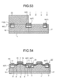
- FIG. 53 is a cross-sectional view for explaining a process of manufacturing the semiconductor device according to the fifth embodiment.
- FIG. 54 is a cross-sectional view of a schematic configuration of a semiconductor device according to a sixth embodiment.
- FIG. 55 is a cross-sectional view for explaining a process of manufacturing the semiconductor device according to the sixth embodiment.
- FIG. 56 is a cross-sectional view for explaining a process of manufacturing the semiconductor device according to the sixth embodiment.
- FIG. 57 is a cross-sectional view for explaining a process of manufacturing the semiconductor device according to the sixth embodiment.
- FIG. 58 is a cross-sectional view for explaining a process of manufacturing the semiconductor device according to the sixth embodiment.
- FIG. 59 is a cross-sectional view for explaining a process of manufacturing the semiconductor device according to the sixth embodiment.
- FIG. 60 is a cross-sectional view for explaining a process of manufacturing the semiconductor device according to the sixth embodiment.
- FIG. 61 is a cross-sectional view for explaining a process of manufacturing the semiconductor device according to the sixth embodiment.
- FIG. 62 is a cross-sectional view for explaining a process of manufacturing the semiconductor device according to the sixth embodiment.
- FIG. 63 is a cross-sectional view for explaining a process of manufacturing the semiconductor device according to the sixth embodiment.
- FIG. 64 is a cross-sectional view for explaining a process of manufacturing the semiconductor device according to the sixth embodiment.
- FIG. 65 is a cross-sectional view for explaining a process of manufacturing the semiconductor device according to the sixth embodiment.
- FIG. 66 is a cross-sectional view for explaining a process of manufacturing the semiconductor device according to the sixth embodiment.
- FIG. 67 is a cross-sectional view for explaining a process of manufacturing the semiconductor device according to the sixth embodiment.
- FIG. 68 is a cross-sectional view of a schematic configuration of a semiconductor device according to a seventh embodiment.
- FIG. 69 is a cross-sectional view for explaining a process of manufacturing the semiconductor device according to the seventh embodiment.
- FIG. 70 is a cross-sectional view for explaining a process of manufacturing the semiconductor device according to the seventh embodiment.
- FIG. 71 is a cross-sectional view for explaining a process of manufacturing the semiconductor device according to the seventh embodiment.
- FIG. 72 is a cross-sectional view for explaining a process of manufacturing the semiconductor device according to the seventh embodiment.
- FIG. 73 is a cross-sectional view for explaining a process of manufacturing the semiconductor device according to the seventh embodiment.
- FIG. 74 is a cross-sectional view for explaining a process of manufacturing the semiconductor device according to the seventh embodiment.
- FIG. 75 is a cross-sectional view for explaining a process of manufacturing the semiconductor device according to the seventh embodiment.
- FIG. 76 is a cross-sectional view for explaining a process of manufacturing the semiconductor device according to the seventh embodiment.
- FIG. 77 is a cross-sectional view for explaining a process of manufacturing the semiconductor device according to the seventh embodiment.
- FIG. 78 is a cross-sectional view for explaining a process of manufacturing the semiconductor device according to the seventh embodiment.
- FIG. 79 is a cross-sectional view for explaining a process of manufacturing the semiconductor device according to the seventh embodiment.
- FIG. 80 is a cross-sectional view for explaining a process of manufacturing the semiconductor device according to the seventh embodiment.
- FIG. 81 is a cross-sectional view for explaining a process of manufacturing the semiconductor device according to the seventh embodiment.
- FIG. 82 is a cross-sectional view for explaining a process of manufacturing the semiconductor device according to the seventh embodiment.
- FIG. 83 is a cross-sectional view for explaining a process of manufacturing the semiconductor device according to the seventh embodiment.
- FIG. 84 is a cross-sectional view for explaining a process of manufacturing the semiconductor device according to the seventh embodiment.
- FIG. 85 is a cross-sectional view for explaining a process of manufacturing the semiconductor device according to the seventh embodiment.
- FIG. 86 is a cross-sectional view of a schematic configuration of a conventional semiconductor device.
- FIG. 87 is a cross-sectional view for explaining a process of manufacturing the conventional semiconductor device.
- FIG. 88 is a cross-sectional view for explaining a process of manufacturing the conventional semiconductor device.
- FIG. 89 is a cross-sectional view for explaining a process of manufacturing the conventional semiconductor device.
- FIG. 90 is a cross-sectional view for explaining a process of manufacturing the conventional semiconductor device.
- FIG. 91 is a cross-sectional view for explaining a process of manufacturing the conventional semiconductor device.
- FIG. 1 is a cross-sectional view of a schematic configuration of a semiconductor device according to a first embodiment of the present invention.
- the semiconductor device includes thin trench-type element isolation structures 30 , 30 ′ having a polysilicon film 4 as a conductive film disposed, via a silicon oxide film 3 , in a trench 2 formed in a silicon substrate 1 as a semiconductor substrate.
- the trench-type element isolation structure 30 includes the polysilicon film 4 formed in the trench 2 on the entire bottom surface of the trench 2 over the total trench width.
- the trench-type element isolation structure 30 ′ includes the polysilicon film 4 formed in the trench 2 only on the sidewall sides on the bottom surface of the trench 2 .
- the polysilicon film 4 is not present near an approximate center of the bottom surface of the trench 2 .
- the height of the polysilicon film 4 is lower than the surface of the silicon substrate 1 .
- a film thickness of the polysilicon film 4 in a lateral direction is constant, and a height of the polysilicon film 4 is lower than the surface of the silicon substrate 1 .
- the film thickness of the polysilicon film 4 in a lateral direction is at least equal to one half of the minimum trench width of the trench 2 .
- the height of the polysilicon film 4 is substantially constant in the entire trench-type element isolation structures 30 , 30 ′, regardless of the width of the trench-type element isolation structure or the trench width of the trench 2 .
- the height of the remaining polysilicon film 4 usually varies by about ⁇ 10% due to a variation in a manufacturing method such as a film formation, CMP, and etching described later.
- a cap oxide film 11 including a silicon oxide film formed by the CVD method is formed on the polysilicon film 4 . Therefore, in the trench-type element isolation structures 30 , 30 ′, a bird's beak is not present in the cap oxide film 11 .
- a gate electrode 7 is formed on the silicon substrate 1 via a gate insulating film 6 .
- a source/drain diffusion layer 8 including a low-concentration impurity diffusion layer self-aligned with the gate electrode 7 via a channel region beneath the gate electrode 7 , and a high-concentration impurity diffusion layer formed at a deeper position self-aligned with the gate electrode and the sidewall.
- the surface of the polysilicon film 4 filled in the trench is lower than the surface of the substrate, and is higher than the lower end of the high-concentration source/drain diffusion layer 8 on the sidewall of the trench.
- the cap oxide film 11 is formed by the CVD method and not by thermal oxidation. Therefore, a bird's beak is not present in the cap oxide film 11 . Accordingly, a reduction in the width of the active region due to the expansion of the cap oxide film 11 to a lateral direction can be prevented. As a result, a conversion difference between a preset shape pattern of a semiconductor device and an actual shape pattern of a manufactured semiconductor device becomes very small. A reduction in the contact margin of a contact between the contact and the active region and a reduction in the driving capacity of transistors can be prevented, which improves the operation speed and productivity. Therefore, a high-quality semiconductor device can be provided.
- the cap oxide film 11 is formed without using oxidation process. Therefore, there is no stress in the semiconductor substrate 1 and the polysilicon film 4 attributable to the oxidation process in the semiconductor substrate 1 and the polysilicon film 4 . Consequently, in the semiconductor device according to the present embodiment, it is possible to prevent the occurrence of a crystal defect due to the oxidation process of the semiconductor substrate 1 and the polysilicon film 4 , and the occurrence of a junction leak current due to a change in band gap attributable to the occurrence of the stress. Therefore, in this semiconductor device, productivity of semiconductor elements can be improved. In other words, a semiconductor device excellent in quality and productivity can be realized.
- the cap oxide film 11 is formed by depositing an oxide film by the CVD method. Therefore, it is possible to prevent thinning or loss of a polysilicon film that is present on the inner wall of the trench having a large trench width. Consequently, reduction in the element isolation capacity attributable to the thinning or loss of the polysilicon film in the trench can be securely prevented. Accordingly, a high-quality semiconductor device capable of stably and effectively performing element isolation can be realized.
- the polysilicon film 4 has a film thickness in a lateral direction at least equal to one half of the minimum trench width of the trench 2 . Therefore, thinning or loss of the polysilicon film present on the inner wall of the trench having a large trench width can be prevented. Consequently, reduction in the element isolation capacity attributable to the thinning or loss of the polysilicon film in the trench can be securely prevented. Accordingly, a high-quality semiconductor device capable of stably and effectively performing element isolation can be realized.
- high concentration means the concentration in which the impurity diffusion layer functions as a source and drain.
- the high concentration means that the concentration of arsenic and phosphor in the case of an NMOS and the concentration of boron in the case of a PMOS are equal to or higher than 1 ⁇ 10 20 /cm 3 .
- Low concentration is lower than this level by about one digit.
- the upper surface of the silicon substrate 1 is thermal oxidized to form a silicon oxide film 9 in a film thickness of about 5 nanometers to 30 nanometers.
- a silicon nitride film 10 is formed in a film thickness of about 50 nanometers to 200 nanometers, on the silicon oxide film 9 .
- a photoresist 21 is patterned to form an opening in which a trench is to be formed, using a photoengraving technique and a dry etching technique, as shown in FIG. 3 .
- the silicon nitride film 10 , the silicon oxide film 9 , and the silicon substrate 1 are anisotropically etched to form the trench 2 , using the photoresist 21 as a mask, and the photoresist 21 is removed.
- FIG. 4 depicts a state after the photoresist 21 is removed.
- the trench 2 has a depth of about 150 nanometers to 500 nanometers from the substrate surface.
- the surface of the inner wall of the trench 2 is thermal oxidized to remove damaged parts of the inner wall of the trench 2 , that is, the inner surface and the bottom surface of the trench 2 .
- the silicon oxide film 3 as an inner wall oxide film or as a protection film is formed on the inner wall of the trench 2 .
- This silicon oxide film 3 is formed in a thickness of about 5 nanometers to 30 nanometers.
- the polysilicon film 4 doped with phosphor is deposited in a film thickness of equal to or larger than one half of a minimum trench width of the trench 2 , on the inner wall of the trench 2 and on the silicon nitride film 10 , by the CVD method, for example.
- a film thickness of the polysilicon film 4 is equal to or larger than one half of the minimum trench width, the polysilicon film 4 is completely filled in the region of the element isolation structure 30 having a small trench width of the trench, as shown in FIG. 6 .
- the polysilicon film 4 is deposited on the bottom and the sidewall of the trench, as shown in FIG. 6 .
- the polysilicon film 4 is deposited in a film thickness smaller than a total of the depth of the trench 2 , the film thickness of the silicon nitride film 10 , and the film thickness of the silicon oxide film 9 .
- the polysilicon film 4 is not filled in an approximate center of the trench 2 , and a space is formed at the center.
- the polysilicon film 4 doped with phosphor is deposited in a film thickness of about 120 nanometers to 200 nanometers.
- a film thickness of the deposited polysilicon film 4 is 150 nanometers
- the polysilicon film 4 is completely filled in a trench area of the trench 2 having a trench width equal to or smaller than 300 nanometers.
- the polysilicon film 4 is deposited on the bottom and the sidewall of the trench part in the trench 2 having a trench width equal to or larger than 300 nanometers. In this case, the polysilicon film 4 is not filled in the approximate center of the trench 2 , and a space is formed at the center.
- the surface of the polysilicon film 4 is polished by the CMP method to remove the polysilicon film 4 on the silicon nitride film 10 as shown in FIG. 7 .
- the polysilicon film 4 is etched back by the anisotropic etching to adjust the height of the surface of the polysilicon film 4 to be lower than the height of the surface of the silicon substrate 1 as shown in FIG. 8 .
- the polysilicon film 4 is deposited in a film thickness smaller than a total of the depth of the trench 2 , the film thickness of the silicon nitride film 10 , and the film thickness of the silicon oxide film 9 .
- the polysilicon film 4 is not filled in the approximate center of the trench 2 , and the silicon oxide film 3 on the trench bottom surface is exposed, in the region of the element isolation structure 30 ′ in which a trench width of the trench is larger than two times the film thickness of polysilicon as shown in FIG. 8 .
- a silicon oxide film 5 is deposited to fill the trench 2 by the CVD (chemical vapor deposition) method, as shown in FIG. 9 .
- the CVD method the high-density plasma CVD (chemical vapor deposition) method (hereinafter, “HDP CVP method”) can be used.
- the entire surface of the silicon oxide film 5 is ground by the CMP method using the silicon nitride film 10 as a stopper.
- the cap oxide film 11 is formed by flattening the silicon oxide film 5 and by removing the silicon oxide film 5 formed on the silicon nitride film 10 , as shown in FIG. 10 .
- the cap oxide film 11 is also filled in a trench 2 ′ formed by the polysilicon film 4 present on the inner wall of the trench 2 , in the region of the element isolation structure 30 ′ in which the trench width of the trench 2 is larger than two times the polysilicon film 4 .
- the silicon oxide film 5 and the silicon oxide film 3 are brought into contact with each other at the approximate center of the bottom surface of the trench 2 .
- a part of the surface of the cap oxide film 11 (the silicon oxide film 5 ) in the trench 2 is removed using hydrofluoric acid, so that the height of the surface of the cap oxide film 11 (the silicon oxide film 5 ) is adjusted as shown in FIG. 11 .
- the silicon nitride film 10 is removed using thermal phosphoric acid, for example.
- the silicon oxide film 9 is removed using hydrofluoric acid to complete the trench-type element isolation structures 30 , 30 ′ as shown in FIG. 12 .
- a well region, a channel-cut region, and a channel impurity layer to control a threshold voltage are formed by the ion implantation method, following the conventionally known MOSFET (Metal Oxide Semiconductor Field Effect Transistor) formation process.
- MOSFET Metal Oxide Semiconductor Field Effect Transistor
- the gate insulating film 6 is formed on the silicon substrate 1 , and a gate electrode material such as polysilicon or tungsten silicide is deposited and patterned on the gate insulating film 6 to form the gate electrode 7 .
- An implantation amount and implantation energy are adjusted using the ion implantation method to form a low-concentration impurity diffusion layer self-aligned with the gate electrode 7 .
- a sidewall 15 is formed on the sidewall of the gate electrode 7 , and a high-concentration impurity diffusion layer is formed at a position deeper than a low-concentration impurity diffusion layer to form the source/drain diffusion layer 8 .
- the lower end of the source/drain region is adjusted to become lower than the height of the surface of the polysilicon film 4 filled in the trench on the sidewall of the trench. As a result, the semiconductor device as shown in FIG. 1 can be manufactured.
- the cap oxide film 11 (the silicon oxide film 5 ) is formed on the polysilicon film 4 by the CVD method and not by thermal oxidation.
- occurrence of a cap oxide film in a lateral direction, that is in a direction approximately parallel with the in-plane direction of the silicon substrate 1 processing can be avoided, unlike in the case of forming a cap oxide film using the conventional oxidation, and a reduction in the width of the active region due to the oxidation of the cap oxide film in the lateral direction can be prevented. Accordingly, a conversion error between a preset shape pattern of a semiconductor device and an actual shape pattern of a manufactured semiconductor device becomes very small. Consequently, a reduction in the contact margin between the contact and the active region and a reduction in the driving capacity of transistors can be prevented, and the operation speed can be improved and the productivity can be improved. Accordingly, a semiconductor device with excellent quality and excellent productivity can be manufactured.
- oxidation process is not used to form the cap oxide film 11 . Therefore, stress is not generated in the semiconductor substrate 1 and the polysilicon film 4 due to a change in their volumes, and stress is not generated in the semiconductor substrate 1 and the polysilicon film 4 due to oxidation.
- a crystal defect does not occur in the semiconductor substrate 1 and the polysilicon film 4 due to the occurrence of stress, and the occurrence of a junction leak current due to a change in the band gap attributable to the occurrence of stress can be prevented.
- the occurrence of a crystal defect can be suppressed, and the occurrence of a junction leak can be decreased, resulting in an improvement in the productivity of semiconductor elements.
- a semiconductor with excellent quality and excellent productivity can be manufactured.
- an oxide film is deposited by the CVD method to form the cap oxide film 11 . Therefore, it is possible to prevent thinning or loss of a polysilicon film that is present on the inner wall of the trench having a large trench width. Consequently, reduction in the element isolation capacity attributable to the thinning or loss of the polysilicon film in the trench can be securely prevented. Accordingly, a high-quality semiconductor device capable of stably and effectively performing element isolation can be realized.
- an oxide film is deposited by the CVD method, and a flattening technique according to the CMP method is used, to form the cap oxide film 11 . Therefore, the surface of the cap oxide film 11 is securely flattened, without generating a gap. Accordingly, occurrence of an etching residual attributable to a surface shape of the cap oxide film 11 can be securely prevented at the time of forming a gate electrode at a later stage, which effectively prevents the short-circuiting of the gate electrode. Consequently, a constraint of the layout of the trench 2 is not necessary to prevent the short-circuiting of the gate electrode, and a semiconductor device having a large degree of flexibility in the layout of the trench 2 can be realized.
- the CMP method and the anisotropic etching are used in combination to remove the polysilicon film 4 . Accordingly, a removal amount of the anisotropic etching can be decreased from that achieved by the conventional method, which decreases damage due to the etching of the bottom surface of the trench 2 . As a result, a highly reliable semiconductor device can be manufactured.
- a film thickness of the polysilicon film 4 in the lateral direction is at least one half of the minimum trench width of the trench 2 in the trench-type element isolation structure 30 ′. Therefore, thinning and loss of a polysilicon film present on the inner wall of the trench can be prevented in the trench having a large trench width. Accordingly, a reduction in the element isolation capacity attributable to the thinning or loss of the polysilicon film in the trench can be securely prevented. Consequently, a high-quality semiconductor device capable of stably and effectively performing the element isolation can be manufactured.
- the lower end of the high-concentration source/drain diffusion layer 8 is formed to be lower than the height of the surface of the polysilicon film 4 filled in the trench on the sidewall of the trench. Therefore, when potentials of adjacent high-concentration source/drain diffusion layers are different, it is possible to effectively suppress the electric field of one diffusion layer from changing the potential of the other diffusion layer.
- a polysilicon film doped with phosphor is explained as a conductive film filled in the trench 2 .
- the conductive film is not limited to this. Instead, it is also possible to use a conductive film such as a polysilicon film (a non-single crystal silicon film doped with a dopant) doped with boron, arsenic, or antimony, a metal film such as tungsten and titanium, and a metal nitride film such as titan nitride and tungsten nitride. In this case, the effect similar to the above can be also obtained.
- FIG. 13 is a cross-sectional view of a schematic configuration of a semiconductor device according to a second embodiment of the present invention.
- This semiconductor device includes a thin trench-type element isolation structure 40 having the polysilicon film 4 as a conductive film disposed, via the silicon oxide film 3 , in the trench 2 formed in the silicon substrate 1 as a semiconductor substrate.
- the trench-type element isolation structure 40 includes the polysilicon film 4 formed in the trench 2 on the entire bottom surface of the trench 2 over the total trench width.
- the height of the polysilicon film 4 is lower than the surface of the silicon substrate 1 .
- a film thickness of the polysilicon film 4 is substantially constant, regardless of the width of the trench-type element isolation structure, that is, regardless of the trench width of the trench 2 .
- the height of the remaining polysilicon film 4 usually varies by about ⁇ 10% due to a variation in a manufacturing method such as a film formation, CMP, and etching described later.
- the cap oxide film 11 including a silicon oxide film formed by the CVD method is formed on the polysilicon film 4 . Therefore, in the trench-type element isolation structures 40 , a bird's beak is not present in the cap oxide film 11 .
- the gate electrode 7 is formed on the silicon substrate 1 via the gate insulating film 6 .
- the source/drain diffusion layer 8 including a low-concentration impurity diffusion layer self-aligned with the gate electrode 7 via a channel region beneath the gate electrode 7 , and a high-concentration impurity diffusion layer formed at a deeper position self-aligned with the gate electrode and the sidewall.
- the surface of the polysilicon film 4 filled in the trench is lower than the surface of the substrate, and is higher than the lower end of the high-concentration source/drain diffusion layer 8 on the sidewall of the trench.
- the cap oxide film 11 is formed by the CVD method and not by thermal oxidation. Therefore, a bird's beak is not present in the cap oxide film 11 . Accordingly, a reduction in the width of the active region due to the expansion of the cap oxide film 11 to a lateral direction can be prevented. As a result, a conversion difference between a preset shape pattern of a semiconductor device and an actual shape pattern of a manufactured semiconductor device becomes very small. A reduction in the contact margin of a contact between the contact and the active region and a reduction in the driving capacity of transistors can be prevented, which improves the operation speed and productivity. Therefore, a high-quality semiconductor device can be provided.
- the cap oxide film 11 is formed without using oxidation process. Therefore, there is no stress in the semiconductor substrate 1 and the polysilicon film 4 attributable to the oxidation process in the semiconductor substrate 1 and the polysilicon film 4 . Consequently, in the semiconductor device according to the present embodiment, it is possible to prevent the occurrence of a crystal defect due to the oxidation process of the semiconductor substrate 1 and the polysilicon film 4 , and the occurrence of a junction leak current due to a change in band gap attributable to the occurrence of the stress. Therefore, in this semiconductor device, productivity of semiconductor elements can be improved. In other words, a semiconductor device excellent in quality and productivity can be realized.
- the cap oxide film 11 is formed by depositing an oxide film by the CVD method. Therefore, it is possible to prevent thinning or loss of a polysilicon film that is present on the inner wall of the trench having a large trench width. Consequently, reduction in the element isolation capacity attributable to the thinning or loss of the polysilicon film in the trench can be securely prevented. Accordingly, a high-quality semiconductor device capable of stably and effectively performing element isolation can be realized.
- the polysilicon film 4 disposed in the trench 2 of the trench-type element isolation structure 40 is formed on the entire bottom surface of the trench 2 over the total trench width. As a result, thinning or loss of the polysilicon film present on the inner wall of the trench can be completely prevented.
- the surface of the polysilicon film 4 is higher than the lower end of the source/drain diffusion layer 8 on the sidewall of the trench. Therefore, when potentials of adjacent high-concentration source/drain diffusion layers are different, it is possible to effectively suppress the electric field of one diffusion layer from changing the potential of the other diffusion layer.
- the upper surface of the silicon substrate 1 is thermal oxidized to form the silicon oxide film 9 in a film thickness of about 5 nanometers to 30 nanometers.
- the silicon nitride film 10 is formed in a film thickness of about 50 nanometers to 200 nanometers, on the silicon oxide film 9 .
- the photoresist 21 is patterned to form an opening in which a trench is to be formed, using a photoengraving technique and a dry etching technique, as shown in FIG. 15 .
- the silicon nitride film 10 , the silicon oxide film 9 , and the silicon substrate 1 are anisotropically etched to form the trench 2 , using the photoresist 21 as a mask, and the photoresist 21 is removed.
- FIG. 16 depicts a state after the photoresist 21 is removed.
- the trench 2 has a depth of about 150 nanometers to 500 nanometers from the substrate surface.
- the surface of the inner wall of the trench 2 is thermal oxidized to remove damaged parts of the inner wall of the trench 2 , that is, the inner surface and the bottom surface of the trench 2 .
- the silicon oxide film 3 as an inner wall oxide film or as a protection film is formed on the inner wall of the trench 2 .
- This silicon oxide film 3 is formed in a thickness of about 5 nanometers to 30 nanometers.
- the polysilicon film 4 doped with phosphor is deposited on the inner wall of the trench 2 and on the silicon nitride film 10 , by the CVD method, for example.
- the polysilicon film 4 is deposited in a film thickness larger than the total of the depth of the trench 2 , the film thickness of the silicon nitride film 10 , and the film thickness of the silicon oxide film 9 .
- all the trenches 2 having various trench widths are filled with the polysilicon film 4 as shown in FIG. 18 . Therefore, in the present embodiment, unlike in the first embodiment, space is not formed without the filling of the polysilicon film 4 in the approximate center of the trench 2 .
- the polysilicon film 4 is formed on the entire bottom surface of the trench 2 over the total trench width.
- the surface of the polysilicon film 4 is polished by the CMP method to remove the polysilicon film 4 on the silicon nitride film 10 as shown in FIG. 17 .
- the polysilicon film 4 is etched back by the anisotropic etching to adjust the height of the surface of the polysilicon film 4 to be lower than the height of the surface of the silicon substrate 1 as shown in FIG. 20 .
- the silicon oxide film 5 is deposited to fill the trench 2 by the CVD method, as shown in FIG. 21 .
- the CVD method the HDP CVP method can be used.
- the entire surface of the silicon oxide film 5 is polished by the CMD method using the silicon nitride film 10 as a stopper.
- the cap oxide film 11 is formed by flattening the silicon oxide film 5 and by removing the silicon oxide film 5 formed on the silicon nitride film 10 , as shown in FIG. 22 .
- a part of the surface of the cap oxide film 11 (the silicon oxide film 5 ) in the trench 2 is removed using hydrofluoric acid, so that the height of the surface of the cap oxide film 11 (the silicon oxide film 5 ) is adjusted as shown in FIG. 23 .
- the silicon nitride film 10 is removed using thermal phosphoric acid, for example.
- the silicon oxide film 9 is removed using hydrofluoric acid to complete the trench-type element isolation structure 40 as shown in FIG. 24 .
- a well region, a channel-cut region, and a channel impurity layer to control a threshold voltage are formed by the ion implantation method, following the conventionally known MOSFET formation process.
- the gate insulating film 6 is formed on the silicon substrate 1 , and a gate electrode material such as polysilicon or tungsten silicide is deposited and patterned on the gate insulating film 6 to form the gate electrode 7 .
- An implantation amount and implantation energy are adjusted using the ion implantation method to form a low-concentration impurity diffusion layer self-aligned with the gate electrode 7 .
- the sidewall 15 is formed on the sidewall of the gate electrode 7 , and a high-concentration impurity diffusion layer is formed at a position deeper than a low-concentration impurity diffusion layer to form the source/drain diffusion layer 8 .
- the lower end of the source/drain region is adjusted to become lower than the height of the surface of the polysilicon film 4 filled in the trench on the sidewall of the trench. As a result, the semiconductor device as shown in FIG. 13 can be manufactured.
- the cap oxide film 11 (the silicon oxide film 5 ) is formed on the polysilicon film 4 by the CVD method and not by thermal oxidation.
- oxidation process is not used to form the cap oxide film 11 . Therefore, stress is not generated in the semiconductor substrate 1 and the polysilicon film 4 due to a change in their volumes, and stress is not generated in the semiconductor substrate 1 and the polysilicon film 4 due to oxidation.
- a crystal defect does not occur in the semiconductor substrate 1 and the polysilicon film 4 due to the occurrence of stress, and the occurrence of a junction leak current due to a change in the band gap attributable to the occurrence of stress can be prevented.
- the occurrence of a crystal defect can be suppressed, and the occurrence of a junction leak can be decreased, resulting in an improvement in the productivity of semiconductor elements.
- a semiconductor with excellent quality and excellent productivity can be manufactured.
- an oxide film is deposited by the CVD method to form the cap oxide film 11 . Therefore, it is possible to prevent thinning or loss of a polysilicon film that is present on the inner wall of the trench having a large trench width. Consequently, reduction in the element isolation capacity attributable to the thinning or loss of the polysilicon film in the trench can be securely prevented. Accordingly, a high-quality semiconductor device capable of stably and effectively performing element isolation can be manufactured.
- an oxide film is deposited by the CVD method, and a flattening technique according to the CMP method is used, to form the cap oxide film 11 . Therefore, the surface of the cap oxide film 11 is securely flattened without generating a gap. Accordingly, occurrence of an etching residual attributable to a surface shape of the cap oxide film 11 can be securely prevented at the time of forming a gate electrode at a later stage, which effectively prevents the short-circuiting of the gate electrode. Consequently, a constraint of the layout of the trench 2 is not necessary to prevent the short-circuiting of the gate electrode, and a semiconductor device having a large degree of flexibility in the layout of the trench 2 can be realized.
- the CMP method and the anisotropic etching are used in combination to remove the polysilicon film 4 . Accordingly, a removal amount of the anisotropic etching can be decreased from that achieved by the conventional method, which decreases damage due to the etching of the bottom surface of the trench 2 . As a result, a highly reliable semiconductor device can be manufactured.
- the polysilicon film 4 is formed on the entire bottom surface of the trench 2 over the total trench width. Therefore, thinning and loss of a polysilicon film present on the inner wall of the trench can be prevented.
- the lower end of the high-concentration source/drain diffusion layer 8 is formed to be lower than the height of the surface of the polysilicon film 4 filled in the trench on the sidewall of the trench. Therefore, when potentials of adjacent high-concentration source/drain diffusion layers are different, it is possible to effectively suppress the electric field of one diffusion layer from changing the potential of the other diffusion layer.
- FIG. 25 is a cross-sectional view of a schematic configuration of a semiconductor device according to a third embodiment of the present invention.
- This semiconductor device includes the thin trench-type element isolation structure 40 having the polysilicon film 4 as a conductive film disposed, via the silicon oxide film 3 , in the trench 2 formed in the silicon substrate 1 as a semiconductor substrate.
- the trench-type element isolation structure 40 includes the polysilicon film 4 formed in the trench 2 on the entire bottom surface of the trench 2 over the total trench width.
- the height of the polysilicon film 4 is lower than the surface of the silicon substrate 1 .
- a film thickness of the polysilicon film 4 is substantially constant, regardless of the width of the trench-type element isolation structure, that is, regardless of the trench width of the trench 2 .
- the height of the remaining polysilicon film 4 usually varies by about ⁇ 10% due to a variation in a manufacturing method such as a film formation, CMP, and etching described later.
- the cap oxide film 11 including a silicon oxide film formed by the CVD method is formed on the polysilicon film 4 . Therefore, in the trench-type element isolation structures 40 , a bird's beak is not present in the cap oxide film 11 .
- the gate electrode 7 is formed on the silicon substrate 1 via the gate insulating film 6 .
- the source/drain diffusion layer 8 via a channel region beneath the gate electrode 7 .
- An interlayer insulating film 12 is formed on the trench-type element isolation structure 40 , on the gate electrode 7 , and on the source/drain diffusion layer 8 , and these interlayer insulating films 12 are connected to wiring layers 14 via contact holes 13 formed in the interlayer insulating films 12 .
- members that are the same as those of the semiconductor device shown in FIG. 13 explained in the first embodiment are denoted with like reference numerals and their detailed explanations will be omitted to facilitate the understanding.
- the semiconductor device according to the present embodiment has effects similar to those of the semiconductor device according to the second embodiment.
- the polysilicon film 4 is formed on the entire bottom surface of the trench 2 over the total trench width. Therefore, there is also an advantage in that the wiring layer 14 can be easily connected to the polysilicon film 4 . Accordingly, potential of the polysilicon film 4 as a conductive film can be securely fixed. For this potential, application of potential in a negative direction from 0 volt is preferable to improve isolation characteristic of a fine N-channel MOS. Because there is a risk of a leakage between the substrate and the conductive film via the silicon oxide film 3 in the trench 2 , application of potential up to about ⁇ 1 volt is preferable. More preferably, an absolute value is equivalent to a power supply voltage (1.0 volt or 1.2 volts) requiring no boosting.
- the height of the surface of the polysilicon film 4 as a conductive film is constant in all the trench-type element isolation structures 40 regardless of the width of the trench-type element isolation structure, that is, the trench width of the trench 2 . Therefore, a connection hole (the contact hole 13 ) to the conductive film can be formed in a region of any isolation width. Capacitance generated parasitically in the source/drain diffusion layer 8 connected to the isolation region does not depend on the width of the trench-type element isolation structure. Therefore, variation in the operation speed can be decreased.
- the upper surface of the silicon substrate 1 is thermal oxidized to form the silicon oxide film 9 in a film thickness of about 5 nanometers to 30 nanometers.
- the silicon nitride film 10 is formed in a film thickness of about 50 nanometers to 200 nanometers, on the silicon oxide film 9 .
- the photoresist 21 is patterned to form an opening in which a trench is to be formed, using a photoengraving technique and a dry etching technique, as shown in FIG. 27 .
- the silicon nitride film 10 , the silicon oxide film 9 , and the silicon substrate 1 are anisotropically etched to form the trench 2 , using the photoresist 21 as a mask, and the photoresist 21 is removed.
- FIG. 28 depicts a state after the photoresist 21 is removed.
- the trench 2 has a depth of about 150 nanometers to 500 nanometers from the substrate surface.
- the surface of the inner wall of the trench 2 is thermal oxidized to remove damaged parts of the inner wall of the trench 2 , that is, the inner surface and the bottom surface of the trench 2 .
- the silicon oxide film 3 as an inner wall oxide film or as a protection film is formed on the inner wall of the trench 2 .
- This silicon oxide film 3 is formed in a thickness of about 5 nanometers to 30 nanometers.
- the polysilicon film 4 doped with phosphor is deposited on the inner wall of the trench 2 and on the silicon nitride film 10 , by the CVD method, for example.
- the polysilicon film 4 is deposited in a film thickness larger than the total of the depth of the trench 2 , the film thickness of the silicon nitride film 10 , and the film thickness of the silicon oxide film 9 .
- all the trenches 2 having various trench widths are filled with the polysilicon film 4 as shown in FIG. 30 .
- the surface of the polysilicon film 4 is polished by the CMP method to remove the polysilicon film 4 on the silicon nitride film 10 as shown in FIG. 31 .
- the polysilicon film 4 is etched back by the anisotropic etching to adjust the height of the surface of the polysilicon film 4 to be lower than the height of the surface of the silicon substrate 1 as shown in FIG. 32 .
- the silicon oxide film 5 is deposited to fill the trench 2 by the CVD method as shown in FIG. 33 .
- the CVD method the HDP CVP method can be used.
- the entire surface of the silicon oxide film 5 is polished by the CMD method using the silicon nitride film 10 as a stopper.
- the cap oxide film 11 is formed by flattening the silicon oxide film 5 and by removing the silicon oxide film 5 formed on the silicon nitride film 10 , as shown in FIG. 34 .
- a part of the surface of the cap oxide film 11 (the silicon oxide film 5 ) in the trench 2 is removed using hydrofluoric acid, so that the height of the surface of the cap oxide film 11 (the silicon oxide film 5 ) is adjusted as shown in FIG. 35 .
- the silicon nitride film 10 is removed using thermal phosphoric acid, for example.
- the silicon oxide film 9 is removed using hydrofluoric acid to complete the trench-type element isolation structure 40 as shown in FIG. 36 .
- a well region, a channel-cut region, and a channel impurity layer to control a threshold voltage are formed by the ion implantation method, following the conventionally known MOSFET formation process.
- the gate insulating film 6 is formed on the silicon substrate 1 , and a gate electrode material such as polysilicon or tungsten silicide is deposited and patterned on the gate insulating film 6 to form the gate electrode 7 .
- An implantation amount and implantation energy are adjusted using the ion implantation method to form a low-concentration impurity diffusion layer self-aligned with the gate electrode 7 .
- the source/drain diffusion layer 8 is formed by the ion implantation method, and the sidewall 15 is formed as shown in FIG. 37 .
- the interlayer insulating film 12 including a silicon oxide film or a lamination film of a silicon oxide film and a silicon nitride film is formed on the silicon substrate 1 .
- Contact holes 13 reaching the gate electrode 7 , the source/drain diffusion layer 8 , and the polysilicon film 4 filled in the trench-type element isolation structure 40 are formed as shown in FIG. 38 .
- Tungsten is filled as a plug material into the contact holes 13 , and the wiring layer 14 is formed by the damascene method.
- the semiconductor device as shown in FIG. 25 is manufactured.
- the method of manufacturing a semiconductor device according to the present embodiment has effects similar to those of the method of manufacturing a semiconductor device according to the second embodiment.
- the polysilicon film 4 is formed on the entire bottom surface of the trench 2 over the total trench width. Therefore, there is also an advantage in that the wiring layer 14 can be easily connected to the polysilicon film 4 . Accordingly, potential of the conductive film can be fixed easily.
- the height of the surface of the polysilicon film 4 as a conductive film is constant in all the trench-type element isolation structures 40 regardless of the width of the trench-type element isolation structure, that is, the trench width of the trench 2 . Therefore, the connection hole (the contact hole 13 ) to the conductive film can be formed in a region of any isolation width.
- the conductive film is provided in the entire region on the bottom surface of the trench.
- a substantially similar effect can be also obtained when the conductive film is not provided in the entire region on the bottom surface of the trench as explained in the first embodiment.
- FIG. 39 is a cross-sectional view of a schematic configuration of a semiconductor device according to a fourth embodiment of the present invention.
- This semiconductor device includes a thin trench-type element isolation structure 50 having the polysilicon film 4 as a conductive film disposed, via the silicon oxide film 3 , in the trench 2 formed in the silicon substrate 1 as a semiconductor substrate.
- the trench-type element isolation structure 40 includes the polysilicon film 4 formed in the trench 2 on the entire bottom surface of the trench 2 over the total trench width.
- the cap oxide film 11 including a silicon oxide film formed by the CVD method is formed on the polysilicon film 4 . Therefore, in the trench-type element isolation structures 50 , a bird's beak is not present in the cap oxide film 11 .
- the gate electrode 7 is formed on the silicon substrate 1 via the gate insulating film 6 .
- the source/drain diffusion layer 8 including a low-concentration impurity diffusion layer self-aligned with the gate electrode 7 via a channel region beneath the gate electrode 7 , and a high-concentration impurity diffusion layer formed at a deeper position self-aligned with the gate electrode and the sidewall.
- FIG. 39 members that are the same as those of the semiconductor device shown in FIG. 1 explained in the first embodiment are denoted with like reference numerals and their detailed explanations will be omitted to facilitate the understanding.
- the polysilicon film 4 filled in the trench 2 is formed in a recess shape on the sidewall of the trench 2 .
- the height of the surface of the polysilicon film 4 present along the sidewall of the trench 2 is lower than the surface of the silicon substrate 1 , and is higher than the lower end of the source/drain diffusion layer 8 .
- the height of the flat part of the polysilicon film 4 in the trench-type element isolation structure 50 is substantially constant in the entire trench-type element isolation structure 50 , regardless of the width of the trench-type element isolation structure 50 , which is the trench width of the trench 2 .
- the height of the remaining polysilicon film 4 usually varies by about ⁇ 10% due to a variation in a manufacturing method such as a film formation, CMP, and etching.
- the semiconductor device according to the present embodiment can be basically manufactured following the method of manufacturing a semiconductor device explained in the second embodiment.
- anisotropy of the etching is slightly decreased, and isotropy is increased to carry out the etching.
- the polysilicon film 4 is etched using etching gas doped with fluorine. As a result, a semiconductor device according to the present embodiment shown in FIG. 39 can be manufactured.
- the cap oxide film 11 having a larger film thickness than that of the upper part of the polysilicon film 4 present along the sidewall of the trench 2 is present on the flat part of the polysilicon film as a conductive film in the trench 2 .
- the cap oxide film 11 having a larger film thickness than that of the upper part of the polysilicon film 4 present along the sidewall of the trench 2 is present on the flat part of the polysilicon film as a conductive film in the trench 2 .
- the effect is obtained that parasitic capacitance can be decreased at the time of forming a wiring layer on the trench-type element isolation structure 50 , as compared with the parasitic capacitance when the height of the polysilicon film 4 in the trench 2 is constant like in the second embodiment.
- a semiconductor device that can carry out a higher-speed operation can be manufactured. Therefore, according to the semiconductor device of the present embodiment, a high-quality semiconductor device with improved operation speed can be provided.
- FIG. 40 is a cross-sectional view of a schematic configuration of a semiconductor device according to a fifth embodiment of the present invention.
- a p-well region 16 doped with a p-type impurity and an n-well region 17 doped with an n-type impurity are formed.
- a thin trench-type element isolation structure 60 in which the polysilicon film 4 as a conductive film is formed is disposed, via the silicon oxide film 3 , in the trench 2 provided in the p-well region 16 and the n-well region 17 .
- the trench-type element isolation structure 60 is formed in the trench 2 on the entire bottom surface over the total trench width.
- the cap oxide film 11 including a silicon oxide film formed by the CVD method is formed on the polysilicon film 4 . Therefore, in the trench-type element isolation structures 60 , a bird's beak is not present in the cap oxide film 11 .
- the gate electrode 7 is formed on the silicon substrate 1 via the gate insulating film 6 .
- the source/drain diffusion layer 8 including a low-concentration impurity diffusion layer self-aligned with the gate electrode 7 via a channel region beneath the gate electrode 7 , and a high-concentration impurity diffusion layer formed at a deeper position self-aligned with the gate electrode and the sidewall.
- an NMOS transistor is formed in the p-well region 16
- a PMOS transistor is formed in the n-well region 17 .
- FIG. 40 members that are the same as those of the semiconductor device shown in FIG. 1 explained in the first embodiment are denoted with like reference numerals and their detailed explanations will be omitted to facilitate the understanding.
- the height of the surface of the polysilicon film 4 filled in the trench 2 is lower than the surface of the silicon substrate 1 , and is higher than the lower end of the high-concentration source/drain diffusion layer 8 on the sidewall of the trench 2 .
- the height of the polysilicon film 4 in the trench-type element isolation structure 60 (film thickness of the polysilicon film 4 in the lateral direction) is substantially constant in the entire trench-type element isolation structure 60 , regardless of the width of the trench-type element isolation structure 60 , which is the trench width of the trench 2 .
- the height of the remaining polysilicon film 4 usually varies by about ⁇ 10% due to a variation in a manufacturing method such as a film formation, CMP, and etching.
- the polysilicon film 4 formed in the trench 2 of the p-well region 16 is a p-type polysilicon film 4 ′ as a p-type conductive film
- the polysilicon film 4 formed in the trench 2 of the n-well region 17 is an n-type polysilicon film 4 ′′ as an n-type conductive film.
- the height of the surface of the polysilicon film 4 filled in the trench 2 is lower than the surface of the silicon substrate 1 , and is also lower than the lower end of the high-concentration source/drain diffusion layer 8 on the sidewall of the trench 2 .
- the semiconductor device according to the present embodiment achieves an effect that the bottom and the sidewall of the trench 2 in the semiconductor substrate 1 is not easily inverted, and the element isolation capacity can be improved, in addition to the effects explained in the second embodiment. Therefore, according to the semiconductor device of the present embodiment, a high-quality semiconductor device with excellent element isolation capacity can be obtained.
- the upper surface of the silicon substrate 1 is thermal oxidized to form the silicon oxide film 9 in a film thickness of about 5 nanometers to 30 nanometers.
- the silicon nitride film 10 is formed in a film thickness of about 50 nanometers to 200 nanometers, on the silicon oxide film 9 .
- the photoresist 21 is patterned to form an opening in which a trench is to be formed, using a photoengraving technique and a dry etching technique, as shown in FIG. 42 .
- the silicon nitride film 10 , the silicon oxide film 9 , and the silicon substrate 1 are anisotropically etched to form the trench 2 , using the photoresist 21 as a mask, and the photoresist 21 is removed.
- FIG. 43 depicts a state after the photoresist 21 is removed.
- the trench 2 has a depth of about 150 nanometers to 500 nanometers from the substrate surface.
- the surface of the inner wall of the trench 2 is thermal oxidized to remove damaged parts of the inner wall of the trench 2 , that is, the inner surface and the bottom surface of the trench 2 .
- the silicon oxide film 3 as an inner wall oxide film or as a protection film is formed on the inner wall of the trench 2 .
- This silicon oxide film 3 is formed in a thickness of about 5 nanometers to 30 nanometers.
- the polysilicon film 4 doped with phosphor is deposited on the inner wall of the trench 2 and on the silicon nitride film 10 , by the CVD method, for example.
- the polysilicon film 4 not doped with an impurity is deposited in a film thickness larger than the total of the depth of the trench 2 , the film thickness of the silicon nitride film 10 , and the film thickness of the silicon oxide film 9 . With this arrangement, a polysilicon film is completely filled in the total trench width of the trench 2 .
- the surface of the polysilicon film 4 is polished by the CMP method to remove the polysilicon film 4 on the silicon nitride film 10 as shown in FIG. 46 .
- the polysilicon film 4 is etched back by the anisotropic etching to adjust the height of the surface of the polysilicon film 4 to be lower than the height of the surface of the silicon substrate 1 as shown in FIG. 47 .
- the silicon oxide film 5 is deposited to fill the trench 2 by the CVD (chemical vapor deposition) method, as shown in FIG. 48 .
- the CVD method the high-density plasma CVD (chemical vapor deposition) method (hereinafter, “HDP CVD method”) can be used.
- the entire surface of the silicon oxide film 5 is polished by the CMD method using the silicon nitride film 10 as a stopper.
- the cap oxide film 11 is formed by flattening the silicon oxide film 5 and by removing the silicon oxide film 5 formed on the silicon nitride film 10 , as shown in FIG. 49 .
- a part of the surface of the cap oxide film 11 (the silicon oxide film 5 ) in the trench 2 is removed using hydrofluoric acid, so that the height of the surface of the cap oxide film 11 (the silicon oxide film 5 ) is adjusted as shown in FIG. 50 .
- the silicon nitride film 10 is removed using thermal phosphoric acid, for example.
- the silicon oxide film 9 is removed using hydrofluoric acid to complete the trench-type element isolation structure 60 as shown in FIG. 51 .
- a resist 22 having an opening that becomes a region of the p-well region 16 is formed as shown in FIG. 52 .
- Boron (B) ion is implanted at multiple stages by changing energy using the resist as a mask.
- the implanting condition the following condition is set, that is, 1 ⁇ 10 13 /cm 2 at 300 kiloelectron volts, 6 ⁇ 10 12 /cm 2 at 100 kiloelectron volts, and 1 ⁇ 10 13 /cm 2 at 10 kiloelectron volts.
- the lower end is formed in the p-well region 16 deeper than the lower surface of the trench 2 .
- boron (B) ion is also implanted into the polysilicon film 4 of the p-well region 16 to form a polysilicon film 4 ′.
- a resist 23 having an opening that becomes a region of the n-well region 17 is formed as shown in FIG. 53 .
- Phosphor (P) ion is implanted at multiple stages by changing energy using the resist as a mask.
- the implanting condition the following condition is set, that is, 1 ⁇ 10 13 /cm 2 at 600 kiloelectron volts, 6 ⁇ 10 12 /cm 2 at 300 kiloelectron volts, and 1 ⁇ 10 13 /cm 2 at 30 kiloelectron volts.
- the lower end is formed in the n-well region 17 deeper than the lower surface of the trench 2 .
- phosphor (P) ion is also implanted into the polysilicon film 4 ′′ of the n-well region 17 to form a polysilicon film 4 ′′.
- the gate insulating film 6 is formed on the silicon substrate 1 , and a gate electrode material such as polysilicon and tungsten silicide is deposited on the gate insulating film 6 , and a patterning is carried out to form the gate electrode 7 , following the conventionally-known MOSFET (Metal Oxide Semiconductor Field Effect Transistor) formation process.
- MOSFET Metal Oxide Semiconductor Field Effect Transistor
- a low-concentration impurity diffusion layer is formed on the gate electrode 7 in a self-aligned manner, and the sidewall 15 is formed on the sidewall of the gate electrode 7 . Thereafter, a high-concentration impurity diffusion layer is formed at a position deeper than the low-concentration impurity diffusion layer, and the source/drain diffusion layer 8 is formed. In the present embodiment, the lower end of the source/drain region is adjusted to become lower than the height of the surface of the polysilicon film 4 filled in the trench 2 on the sidewall of the trench 2 .
- an NMOS transistor is formed in the p-well region 16
- a PMOS transistor is formed in the n-well region 17 , by separating conductivity of the impurities to be introduced.
- a semiconductor device as shown in FIG. 40 can be manufactured.
- polysilicon in the trench 2 of the p-well region 16 is formed as a p-type polysilicon film 4 ′ doped in the p-type
- polysilicon in the trench 2 of the n-well region 17 is formed as the n-type polysilicon film 4 ′′ doped in the n-type.
- FIG. 54 is a cross-sectional view of a schematic configuration of a semiconductor device according to a sixth embodiment of the present invention.
- the p-well region 16 doped with a p-type impurity and the n-well region 17 doped with an n-type impurity are formed.
- the trench 2 provided in the p-well region 16 and the n-well region 17 includes within thin trench-type element isolation structures 70 , 70 ′, 70 ′′ in which the polysilicon film 4 as a conductive film is disposed via the silicon oxide film 3 .
- the trench-type element isolation structures 70 ′, 70 ′′ are disposed on the entire bottom surface of the trench 2 over the total trench width.
- the polysilicon film 4 ( 4 ′, 4 ′′) in the trench 2 is formed only on the sidewall sides on the bottom surface of the trench 2 , and is not present near the approximate center of the bottom surface of the trench 2 .
- the cap oxide film 11 including a silicon oxide film formed by the CVD method is formed on the polysilicon film 4 . Therefore, in the trench-type element isolation structures 70 , 70 ′, 70 ′′, a bird's beak is not present in the cap oxide film 11 .
- the gate electrode 7 is formed on the silicon substrate 1 via the gate insulating film 6 .
- the source/drain diffusion layer 8 including a low-concentration impurity diffusion layer self-aligned with the gate electrode 7 via a channel region beneath the gate electrode 7 , and a high-concentration impurity diffusion layer formed at a deeper position self-aligned with the gate electrode and the sidewall.
- an NMOS transistor is formed in the p-well region 16
- a PMOS transistor is formed in the n-well region 17 .
- the height of the surface of the polysilicon film 4 filled in the trench 2 is lower than the surface of the silicon substrate 1 , and is higher than the lower end of the high-concentration source/drain diffusion layer 8 on the sidewall of the trench.
- the height of the polysilicon film 4 in the trench-type element isolation structures 70 , 70 ′, 70 ′′ is substantially constant in the entire trench-type element isolation structures 70 , 70 ′, 70 ′′, regardless of the width of the trench-type element isolation structures 70 , 70 ′, 70 ′′, that is the trench width of the trench 2 .
- the height of the remaining polysilicon film 4 usually varies by about ⁇ 10% due to a variation in a manufacturing method such as a film formation, CMP, and etching.
- the polysilicon film 4 formed in the trench 2 of the p-well region 16 is the p-type polysilicon film 4 ′ as a p-type conductive film
- the polysilicon film 4 formed in the trench 2 of the n-well region 17 is the n-type polysilicon film 4 ′′ as an n-type conductive film.
- polysilicon in the trench 2 of the p-well region 16 is formed as the p-type polysilicon film 4 ′ doped in the p-type
- polysilicon in the trench 2 of the n-well region 17 is formed as the n-type polysilicon film 4 ′′ doped in the n-type.
- the polysilicon film 4 ′ and the polysilicon film 4 ′′ having different conductivities are completely separated from each other.
- the semiconductor device according to the present embodiment achieves an effect that interference between conductive films, that is, between the polysilicon film 4 ′ and the polysilicon film 4 ′′, can be prevented, in addition to the effects explained in the third and fifth embodiments, thereby improving stability of transistor elements. Therefore, according to the semiconductor device of the present embodiment, a high-quality semiconductor device with excellent stability of operation is realized.
- the upper surface of the silicon substrate 1 is thermal oxidized to form the silicon oxide film 9 in a film thickness of about 5 nanometers to 30 nanometers.
- the silicon nitride film 10 is formed in a film thickness of about 50 nanometers to 200 nanometers, on the silicon oxide film 9 .
- the photoresist 21 is patterned to form an opening in which a trench is to be formed, using a photoengraving technique and a dry etching technique, as shown in FIG. 56 .
- the silicon nitride film 10 , the silicon oxide film 9 , and the silicon substrate 1 are anisotropically etched to form the trench 2 , using the photoresist 21 as a mask, and the photoresist 21 is removed.
- FIG. 57 depicts a state after the photoresist 21 is removed.
- the trench 2 has a depth of about 150 nanometers to 500 nanometers from the substrate surface.
- the surface of the inner wall of the trench 2 is thermal oxidized to remove damaged parts of the inner wall of the trench 2 , that is, the inner surface and the bottom surface of the trench 2 .
- the silicon oxide film 3 as an inner wall oxide film or as a protection film is formed on the inner wall of the trench 2 .
- This silicon oxide film 3 is formed in a thickness of about 5 nanometers to 30 nanometers.
- the polysilicon film 4 not doped with an impurity is deposited on the inner wall of the trench 2 and on the silicon nitride film 10 , in a film thickness of equal to or larger than one half of the minimum trench width of the trench 2 , by the CVD method, for example.
- the film thickness of the polysilicon film 4 is equal to or larger than one half of the minimum trench width of the trench 2
- the polysilicon film 4 is completely filled in the region of the element isolation structures 70 ′, 70 ′′ in which the trench width of the trench is small as shown in FIG. 59 .
- the polysilicon film 4 is deposited on the bottom surface and the sidewall of the trench as shown in FIG. 59 .
- the polysilicon film 4 is deposited in a film thickness smaller than a total of the depth of the trench 2 , the film thickness of the silicon nitride film 10 , and the film thickness of the silicon oxide film 9 .
- the polysilicon film 4 is not filled in the approximate center of the trench 2 , and a space is formed.
- the polysilicon film 4 doped with phosphor is deposited in a film thickness of about 120 nanometers to 200 nanometers.
- a film thickness of the deposited polysilicon film 4 is 150 nanometers
- the polysilicon film 4 is completely filled in a trench area of the trench 2 having a trench width equal to or smaller than 300 nanometers.
- the polysilicon film 4 is deposited on the bottom and the sidewall of the trench part in the trench 2 having a trench width equal to or larger than 300 nanometers. In this case, the polysilicon film 4 is not filled in the approximate center of the trench 2 , and a space is formed at the center.
- the surface of the polysilicon film 4 is polished by the CMP method to remove the polysilicon film 4 on the silicon nitride film 10 as shown in FIG. 60 .
- the polysilicon film 4 is etched back by the anisotropic etching to adjust the height of the surface of the polysilicon film 4 to be lower than the height of the surface of the silicon substrate 1 as shown in FIG. 61 .
- the polysilicon film 4 at the center of the bottom of the trench having a large trench width is also removed. Therefore, the polysilicon film 4 remains on only the sidewall of the trench.
- the polysilicon film 4 is deposited in a film thickness smaller than a total of the depth of the trench 2 , the film thickness of the silicon nitride film 10 , and the film thickness of the silicon oxide film 9 .
- the polysilicon film 4 is not filled in the approximate center of the trench 2 , and the silicon oxide film 3 on the trench bottom surface is exposed, in the region of the element isolation structure 70 in which a trench width of the trench is larger than two times the film thickness of polysilicon, as shown in FIG. 61 .
- the silicon oxide film 5 is deposited to embed the trench 2 by the CVD (chemical vapor deposition) method, as shown in FIG. 62 .
- CVD chemical vapor deposition
- the high-density plasma CVD (chemical vapor deposition) method hereinafter, “HDP CVP method”.
- the entire surface of the silicon oxide film 5 is polished by the CMD method using the silicon nitride film 10 as a stopper.
- the cap oxide film 11 is formed by flattening the silicon oxide film 5 and by removing the silicon oxide film 5 formed on the silicon nitride film 10 , as shown in FIG. 63 .
- the cap oxide film 11 is also filled in the trench 2 ′ formed by the polysilicon film 4 present on the inner wall of the trench 2 , in the region of the element isolation structure 70 in which the trench width of the trench 2 is larger than two times the polysilicon film 4 .
- the silicon oxide film 5 and the silicon oxide film 3 are brought into contact with each other at the approximate center of the bottom surface of the trench 2 .
- a part of the surface of the cap oxide film 11 (the silicon oxide film 5 ) in the trench 2 is removed using hydrofluoric acid to adjust the height of the surface of the cap oxide film 11 (the silicon oxide film 5 ) as shown in FIG. 64 .
- the silicon nitride film 10 is removed using thermal phosphoric acid, for example.
- the silicon oxide film 9 is removed using hydrofluoric acid to complete the trench-type element isolation structures 70 , 70 ′, 70 ′′ as shown in FIG. 65 .
- the resist 22 having an opening that becomes a region of the p-well region 16 is formed as shown in FIG. 66 .
- Boron (B) ion is implanted at multiple stages by changing energy using the resist as a mask.
- the implanting condition the following condition is set, that is 1 ⁇ 10 13 /cm 2 at 300 kiloelectron volts, 6 ⁇ 10 12 /cm 2 at 100 kiloelectron volts, and 1 ⁇ 10 13 /cm 2 at 10 kiloelectron volts.
- the lower end is formed in the p-well region 16 deeper than the lower surface of the trench 2 .
- boron (B) ion is also implanted into the polysilicon film 4 of the p-well region 16 to form the polysilicon film 4 ′.
- the resist 23 having an opening that becomes a region of the n-well region 17 is formed as shown in FIG. 67 .
- Phosphor (P) ion is implanted at multiple stages by changing energy using the resist as a mask.
- the implanting condition the following condition is set, that is, 1 ⁇ 10 13 /cm 2 at 600 kiloelectron volts, 6 ⁇ 10 12 /cm 2 at 300 kiloelectron volts, and 1 ⁇ 10 13 /cm 2 at 30 kiloelectron volts.
- the lower end is formed in the n-well region 17 deeper than the lower surface of the trench 2 .
- phosphor (P) ion is also implanted into the polysilicon film 4 ′′ of the n-well region 17 to form the polysilicon film 4 ′′.
- the gate insulating film 6 is formed on the silicon substrate 1 , and a gate electrode material such as polysilicon and tungsten silicide is deposited on the gate insulating film 6 , and a patterning is carried out to form the gate electrode 7 , following the conventionally-known MOSFET (Metal Oxide Semiconductor Field Effect Transistor) formation process.
- MOSFET Metal Oxide Semiconductor Field Effect Transistor
- a low-concentration impurity diffusion layer is formed on the gate electrode 7 in a self-aligned manner, and the sidewall 15 is formed on the sidewall of the gate electrode 7 . Thereafter, a high-concentration impurity diffusion layer is formed at a position deeper than the low-concentration impurity diffusion layer to form the source/drain diffusion layer 8 .
- the lower end of the source/drain region is adjusted to become lower than the height of the surface of the polysilicon film 4 filled in the trench 2 on the sidewall of the trench 2 .
- an NMOS transistor is formed in the p-well region 16
- a PMOS transistor is formed in the n-well region 17 , by separating conductivity of the impurities to be introduced.
- a semiconductor device as shown in FIG. 54 can be manufactured.
- polysilicon in the trench 2 of the p-well region 16 is formed as the p-type polysilicon film 4 ′ doped in the p-type
- polysilicon in the trench 2 of the n-well region 17 is formed as the n-type polysilicon film 4 ′′ doped in the n-type.
- the polysilicon film 4 ′ and the polysilicon film 4 ′′ having different conductivities are completely separated from each other.
- the semiconductor device according to the present embodiment achieves an effect that interference between conductive films, that is, between the polysilicon film 4 ′ and the polysilicon film 4 ′′, can be prevented, in addition to the effects explained in the third and fifth embodiments, thereby improving stability of transistor elements. Therefore, in the method of manufacturing a semiconductor device according to the present embodiment, a high-quality semiconductor device with excellent stability of operation is realized.
- FIG. 68 is a cross-sectional view of a schematic configuration of a semiconductor device according to a seventh embodiment of the present invention.
- the p-well region 16 doped with a p-type impurity and the n-well region 17 doped with an n-type impurity are formed.
- the trench 2 provided in the p-well region 16 and the n-well region 17 includes in this trench the thin trench-type element isolation structures 70 , 70 ′, 70 ′′ in which the polysilicon film 4 as a conductive film is disposed via the silicon oxide film 3 .
- the trench-type element isolation structures 70 ′, 70 ′′ are formed on the entire bottom surface of the trench 2 over the total trench width.
- the polysilicon film 4 ( 4 ′, 4 ′′) in the trench 2 is formed only on the sidewall sides on the bottom surface of the trench 2 , and is not present near the approximate center of the bottom surface of the trench 2 .
- the cap oxide film 11 including a silicon oxide film formed by the CVD method is formed on the polysilicon film 4 . Therefore, in the trench-type element isolation structures 70 , 70 ′, 70 ′′, a bird's beak is not present in the cap oxide film 11 .
- the gate electrode 7 is formed on the silicon substrate 1 via the gate insulating film 6 .
- the source/drain diffusion layer 8 including a low-concentration impurity diffusion layer self-aligned with the gate electrode 7 via a channel region beneath the gate electrode 7 , and a high-concentration impurity diffusion layer formed at a deeper position self-aligned with the gate electrode and the sidewall.
- an NMOS transistor is formed in the p-well region 16
- a PMOS transistor is formed in the n-well region 17 .
- the interlayer insulating film 12 is formed on the trench-type element isolation structures 70 , 70 ′, 70 ′′, on the gate electrode 7 , and on the source/drain diffusion layer 8 , and these interlayer insulating films 12 are connected to the wiring layer 14 via the contact holes 13 formed in the interlayer insulating films 12 .
- the height of the surface of the polysilicon film 4 filled in the trench 2 is lower than the surface of the silicon substrate 1 , and is higher than the lower end of the high-concentration source/drain diffusion layer 8 on the sidewall of the trench.
- the height of the polysilicon film 4 in the trench-type element isolation structures 70 , 70 ′, 70 ′′ is substantially constant in the entire trench-type element isolation structures 70 , 70 ′, 70 ′′, regardless of the width of the trench-type element isolation structures 70 , 70 ′, 70 ′′, that is the trench width of the trench 2 .
- the height of the remaining polysilicon film 4 usually varies by about ⁇ 10% due to a variation in a manufacturing method such as a film formation, CMP, and etching.
- the polysilicon film 4 formed in the trench 2 of the p-well region 16 is the p-type polysilicon film 4 ′ as a p-type conductive film
- the polysilicon film 4 formed in the trench 2 of the n-well region 17 is the n-type polysilicon film 4 ′′ as an n-type conductive film.
- polysilicon in the trench 2 of the p-well region 16 is formed as the p-type polysilicon film 4 ′ doped in the p-type
- polysilicon in the trench 2 of the n-well region 17 is formed as the n-type polysilicon film 4 ′′ doped in the n-type.
- the polysilicon film 4 ′ and the polysilicon film 4 ′′ having different conductivities are completely separated from each other. These polysilicon films 4 ( 4 ′, 4 ′′) are connected to the wiring layer 14 via the contact 13 , and can be fixed at different potentials.
- the semiconductor device according to the present embodiment achieves an effect that an optimum voltage can be applied to each of the trench-type element isolation structure in the p-well region 16 and the trench-type element isolation structure in the n-well region 17 , in addition to the effects explained in the third, fifth, and sixth embodiments, thereby improving the isolation characteristics by the trench-type element isolation. Therefore, according to the semiconductor device of the present embodiment, a high-quality semiconductor device with excellent stability of operation is realized.
- the absolute value is equivalent to or lower than the power supply voltage.
- the upper surface of the silicon substrate 1 is thermal oxidized to form the silicon oxide film 9 in a film thickness of about 5 nanometers to 30 nanometers.
- the silicon nitride film 10 is formed in a film thickness of about 50 nanometers to 200 nanometers, on the silicon oxide film 9 .
- the photoresist 21 is patterned to form an opening in which a trench is to be formed, using a photoengraving technique and a dry etching technique, as shown in FIG. 70 .
- the silicon nitride film 10 , the silicon oxide film 9 , and the silicon substrate 1 are anisotropically etched to form the trench 2 , using the photoresist 21 as a mask, and the photoresist 21 is removed.
- FIG. 71 depicts a state after the photoresist 21 is removed.
- the trench 2 has a depth of about 150 nanometers to 500 nanometers from the substrate surface.
- the surface of the inner wall of the trench 2 is thermal oxidized to remove damaged parts of the inner wall of the trench 2 , that is, the inner surface and the bottom surface of the trench 2 .
- the silicon oxide film 3 as an inner wall oxide film or as a protection film is formed on the inner wall of the trench 2 .
- This silicon oxide film 3 is formed in a thickness of about 5 nanometers to 30 nanometers.
- the polysilicon film 4 not doped with an impurity is deposited on the inner wall of the trench 2 and on the silicon nitride film 10 , in a film thickness of equal to or larger than one half of the minimum trench width of the trench 2 , by the CVD method, for example.
- the film thickness of the polysilicon film 4 is equal to or larger than one half of the minimum trench width of the trench 2
- the polysilicon film 4 is completely filled in the region of the element isolation structures 70 ′, 70 ′′ in which the trench width of the trench is small as shown in FIG. 73 .
- the polysilicon film 4 is deposited on the bottom surface and the sidewall of the trench as shown in FIG. 73 .
- the polysilicon film 4 is deposited in a film thickness smaller than a total of the depth of the trench 2 , the film thickness of the silicon nitride film 10 , and the film thickness of the silicon oxide film 9 .
- the polysilicon film 4 is not filled in the approximate center of the trench 2 , and a space is formed.
- the polysilicon film 4 doped with phosphor is deposited in a film thickness of about 120 nanometers to 200 nanometers.
- a film thickness of the deposited polysilicon film 4 is 150 nanometers
- the polysilicon film 4 is completely filled in a trench area of the trench 2 having a trench width equal to or smaller than 300 nanometers.
- the polysilicon film 4 is deposited on the bottom and the sidewall of the trench part in the trench 2 having a trench width equal to or larger than 300 nanometers. In this case, the polysilicon film 4 is not filled in the approximate center of the trench 2 , and a space is formed at the center.
- the surface of the polysilicon film 4 is polished by the CMP method to remove the polysilicon film 4 on the silicon nitride film 10 as shown in FIG. 74 .
- the polysilicon film 4 is etched back by the anisotropic etching to adjust the height of the surface of the polysilicon film 4 to be lower than the height of the surface of the silicon substrate 1 as shown in FIG. 75 .
- the polysilicon film 4 at the center of the bottom of the trench having a large trench width is also removed. Therefore, the polysilicon film 4 remains on only the sidewall of the trench.
- the polysilicon film 4 is deposited in a film thickness smaller than a total of the depth of the trench 2 , the film thickness of the silicon nitride film 10 , and the film thickness of the silicon oxide film 9 .
- the polysilicon film 4 is not filled in the approximate center of the trench 2 , and the silicon oxide film 3 on the trench bottom surface is exposed, in the region of the element isolation structure 70 in which a trench width of the trench is larger than two times the film thickness of polysilicon, as shown in FIG. 75 .
- the silicon oxide film 5 is deposited to fill the trench 2 by the CVD (chemical vapor deposition) method, as shown in FIG. 76 .
- CVD chemical vapor deposition
- the high-density plasma CVD (chemical vapor deposition) method hereinafter, “the HDP CVP method” can be used.
- the entire surface of the silicon oxide film 5 is polished by the CMD method using the silicon nitride film 10 as a stopper.
- the cap oxide film 11 is formed by flattening the silicon oxide film 5 and by removing the silicon oxide film 5 formed on the silicon nitride film 10 , as shown in FIG. 77 .
- the cap oxide film 11 is also filled in the trench 2 ′ formed by the polysilicon film 4 present on the inner wall of the trench 2 , in the region of the element isolation structure 70 in which the trench width of the trench 2 is larger than two times the polysilicon film 4 .
- the silicon oxide film 5 and the silicon oxide film 3 are brought into contact with each other at the approximate center of the bottom surface of the trench 2 .
- a part of the surface of the cap oxide film 11 (the silicon oxide film 5 ) in the trench 2 is removed using hydrofluoric acid, so that the height of the surface of the cap oxide film 11 (the silicon oxide film 5 ) is adjusted as shown in FIG. 78 .
- the silicon nitride film 10 is removed using thermal phosphoric acid, for example.
- the silicon oxide film 9 is removed using hydrofluoric acid to complete the trench-type element isolation structures 70 , 70 ′, 70 ′′ as shown in FIG. 79 .
- the resist 22 having an opening that becomes a region of the p-well region 16 is formed as shown in FIG. 80 .
- Boron (B) ion is implanted at multiple stages by changing energy using the resist as a mask.
- the implanting condition the following condition is set, that is, 1 ⁇ 10 13 /cm 2 at 300 kiloelectron volts, 6 ⁇ 10 12 /cm 2 at 100 kiloelectron volts, and 1 ⁇ 10 13 /cm 2 at 10 kiloelectron volts.
- the lower end is formed in the p-well region 16 deeper than the lower surface of the trench 2 .
- boron (B) ion is also implanted into the polysilicon film 4 of the p-well region 16 to form the polysilicon film 4 ′.
- the resist 23 having an opening that becomes a region of the n-well region 17 is formed as shown in FIG. 81 .
- Phosphor (P) ion is implanted at multiple stages by changing energy using the resist as a mask.
- the implanting condition the following condition is set, that is, 1 ⁇ 10 13 /cm 2 at 600 kiloelectron volts, 6 ⁇ 10 12 /cm 2 at 300 kiloelectron volts, and 1 ⁇ 10 13 /cm 2 at 30 kiloelectron volts.
- the lower end is formed in the n-well region 17 deeper than the lower surface of the trench 2 .
- phosphor (P) ion is also implanted into the polysilicon film 4 ′′ of the n-well region 17 to form the polysilicon film 4 ′′.
- the gate insulating film 6 is formed on the silicon substrate 1 , and a gate electrode material such as polysilicon and tungsten silicide is deposited on the gate insulating film 6 , and a patterning is carried out to form the gate electrode 7 , following the conventionally-known MOSFET (Metal Oxide Semiconductor Field Effect Transistor) formation process.
- MOSFET Metal Oxide Semiconductor Field Effect Transistor
- a low-concentration impurity diffusion layer is formed on the gate electrode 7 in a self-aligned manner, and the sidewall 15 is formed on the sidewall of the gate electrode 7 . Thereafter, a high-concentration impurity diffusion layer is formed at a position deeper than the low-concentration impurity diffusion layer to form the source/drain diffusion layer 8 .
- the lower end of the source/drain region is adjusted to become lower than the height of the surface of the polysilicon film 4 filled in the trench 2 on the sidewall of the trench.
- the sidewall 15 is formed as shown in FIG. 82 . In this case, using a photoengraving technique, an NMOS transistor is formed in the p-well region 16 , and a PMOS transistor is formed in the n-well region 17 , by separating conductivity of the impurities to be introduced.
- the interlayer insulating film 12 including a silicon oxide film or a lamination film of a silicon oxide film and a silicon nitride film is formed on the silicon substrate 1 .
- the contact holes 13 reaching the gate electrode 7 , the source/drain diffusion layer 8 , and the polysilicon film 4 filled in the trench-type element isolation structures 70 , 70 ′, 70 ′′ are formed as shown in FIG. 83 .
- Tungsten is filled as a plug material into the contact holes 13 , and the wiring layer 14 is formed by the damascene method.
- the semiconductor device as shown in FIG. 68 is manufactured.
- polysilicon in the trench 2 of the p-well region 16 is formed as the p-type polysilicon film 4 ′ doped in the p-type
- polysilicon in the trench 2 of the n-well region 17 is formed as the n-type polysilicon film 4 ′′ doped in the n-type.
- the polysilicon film 4 ′ and the polysilicon film 4 ′′ having different conductivities are completely separated from each other. These polysilicon films 4 ( 4 ′, 4 ′′) are connected to the wiring layer 14 via the contact 13 , and can be fixed at different potentials.
- the semiconductor device according to the present embodiment achieves an effect that an optimum voltage can be applied to each of the trench-type element isolation structure in the p-well region 16 and the trench-type element isolation structure in the n-well region 17 , in addition to the effects explained in the third, fifth, and sixth embodiments, thereby improving the isolation characteristics by the trench-type element isolation. Therefore, in the method of manufacturing a semiconductor device according to the present embodiment, a high-quality semiconductor device with excellent isolation characteristic can be manufactured.
- potential fixing region in the conductive layer potential can be fixed for only one of the conductive layer in the region of the p-well region 16 and the conductive layer in the region of the n-well region 17 .
- a region in which potential is fixed and a floating region can be mixed in the same chip.
- potential can be fixed, and a memory region having no space to form a contact can be set as a floating region.
- FIG. 84 is a cross-sectional view of a modification of a connection between a conductive film and a wiring in the trench 2 .
- the contact 13 for connecting between the polysilicon film 4 as a conductive layer and the wiring layer 14 is formed on at least a part of the upper part of the polysilicon film 4 as a conductive film in the trench 2 and a part of the sidewall of the polysilicon film 4 .
- a contact area between a plug material (conductive film) constituting the contact 13 and the polysilicon film 4 as a conductive film in the trench 2 becomes large, which enables a stable electric connection.
- a region in which the contact 13 overlaps the polysilicon film 4 in the trench 2 can be decreased, which enables less area of semiconductor chips and smaller semiconductor chips.
- FIG. 85 is a top plan view of an example of a layout of the contact 13 .
- the contact 13 for connecting between the polysilicon films 4 ( 4 ′, 4 ′′) as conductive layers in the trench 2 and the wiring layer 14 is formed on at least a part of the upper part of the polysilicon films 4 ( 4 ′, 4 ′′) and a part of the sidewall of the polysilicon films 4 ( 4 ′, 4 ′′).
- the contacts 13 are not on the same line in the side direction of the trench 2 . In other words, the fact that the contacts 13 are not on the same line in a direction of a long side of the trench 2 (the X direction in FIG.
- FIG. 85 is a view that a part of the wiring layer 14 , the interlayer insulating film 12 , and the cap oxide film 11 is transparent.
- the method of manufacturing a semiconductor device according to the present invention is useful to manufacture a semiconductor device having a trench-type element isolation structure.
- the method of manufacturing a semiconductor device is suitable for the manufacturing of a semiconductor device having a conductive film embedded in an element isolation trench to prevent potentials of adjacent elements from affecting other nodes via the embedded oxide film.
Landscapes
- Element Separation (AREA)
- Insulated Gate Type Field-Effect Transistor (AREA)
- Internal Circuitry In Semiconductor Integrated Circuit Devices (AREA)
- Metal-Oxide And Bipolar Metal-Oxide Semiconductor Integrated Circuits (AREA)
- Electrodes Of Semiconductors (AREA)
Abstract
Description
Claims (19)
Priority Applications (1)
| Application Number | Priority Date | Filing Date | Title |
|---|---|---|---|
| US12/840,430 US8043918B2 (en) | 2004-10-25 | 2010-07-21 | Semiconductor device and its manufacturing method |
Applications Claiming Priority (5)
| Application Number | Priority Date | Filing Date | Title |
|---|---|---|---|
| JP2004-310151 | 2004-10-25 | ||
| JP2004310151 | 2004-10-25 | ||
| PCT/JP2005/019141 WO2006046442A1 (en) | 2004-10-25 | 2005-10-18 | Semiconductor device and its manufacturing method |
| US57787807A | 2007-04-25 | 2007-04-25 | |
| US12/840,430 US8043918B2 (en) | 2004-10-25 | 2010-07-21 | Semiconductor device and its manufacturing method |
Related Parent Applications (3)
| Application Number | Title | Priority Date | Filing Date |
|---|---|---|---|
| US11/577,878 Division US7791163B2 (en) | 2004-10-25 | 2005-10-18 | Semiconductor device and its manufacturing method |
| PCT/JP2005/019141 Division WO2006046442A1 (en) | 2004-10-25 | 2005-10-18 | Semiconductor device and its manufacturing method |
| US57787807A Division | 2004-10-25 | 2007-04-25 |
Publications (2)
| Publication Number | Publication Date |
|---|---|
| US20100285651A1 US20100285651A1 (en) | 2010-11-11 |
| US8043918B2 true US8043918B2 (en) | 2011-10-25 |
Family
ID=36227684
Family Applications (2)
| Application Number | Title | Priority Date | Filing Date |
|---|---|---|---|
| US11/577,878 Expired - Fee Related US7791163B2 (en) | 2004-10-25 | 2005-10-18 | Semiconductor device and its manufacturing method |
| US12/840,430 Expired - Fee Related US8043918B2 (en) | 2004-10-25 | 2010-07-21 | Semiconductor device and its manufacturing method |
Family Applications Before (1)
| Application Number | Title | Priority Date | Filing Date |
|---|---|---|---|
| US11/577,878 Expired - Fee Related US7791163B2 (en) | 2004-10-25 | 2005-10-18 | Semiconductor device and its manufacturing method |
Country Status (6)
| Country | Link |
|---|---|
| US (2) | US7791163B2 (en) |
| JP (1) | JP5234886B2 (en) |
| KR (1) | KR20070072928A (en) |
| CN (1) | CN101069279B (en) |
| TW (1) | TWI389249B (en) |
| WO (1) | WO2006046442A1 (en) |
Families Citing this family (17)
| Publication number | Priority date | Publication date | Assignee | Title |
|---|---|---|---|---|
| JP2007194259A (en) * | 2006-01-17 | 2007-08-02 | Toshiba Corp | Semiconductor device and manufacturing method thereof |
| US7723204B2 (en) * | 2006-03-27 | 2010-05-25 | Freescale Semiconductor, Inc. | Semiconductor device with a multi-plate isolation structure |
| JP2008004881A (en) * | 2006-06-26 | 2008-01-10 | Oki Electric Ind Co Ltd | Method for manufacturing element isolation structure |
| KR100790296B1 (en) * | 2006-12-04 | 2008-01-02 | 주식회사 하이닉스반도체 | Manufacturing Method of Flash Memory Device |
| DE102007004884A1 (en) * | 2007-01-31 | 2008-08-14 | Advanced Micro Devices, Inc., Sunnyvale | A method of forming a metal layer over a patterned dielectric by electroless deposition using a selectively provided activation layer |
| JP5350681B2 (en) * | 2008-06-03 | 2013-11-27 | ルネサスエレクトロニクス株式会社 | Semiconductor device |
| JP5691074B2 (en) | 2008-08-20 | 2015-04-01 | ルネサスエレクトロニクス株式会社 | Manufacturing method of semiconductor device |
| JP4685147B2 (en) * | 2008-10-14 | 2011-05-18 | エルピーダメモリ株式会社 | Manufacturing method of semiconductor device |
| JP2011096829A (en) * | 2009-10-29 | 2011-05-12 | Elpida Memory Inc | Method of forming semiconductor device |
| US20110115047A1 (en) * | 2009-11-13 | 2011-05-19 | Francois Hebert | Semiconductor process using mask openings of varying widths to form two or more device structures |
| JP2012222285A (en) | 2011-04-13 | 2012-11-12 | Elpida Memory Inc | Semiconductor device and method of manufacturing the same |
| US8673737B2 (en) | 2011-10-17 | 2014-03-18 | International Business Machines Corporation | Array and moat isolation structures and method of manufacture |
| CN105845729B (en) * | 2015-01-15 | 2019-04-09 | 中芯国际集成电路制造(上海)有限公司 | A semiconductor device and its manufacturing method and electronic device |
| WO2018159186A1 (en) * | 2017-02-28 | 2018-09-07 | 富士フイルム株式会社 | Semiconductor device, laminate, semiconductor device manufacturing method, and laminate manufacturing method |
| KR102879031B1 (en) * | 2020-01-15 | 2025-10-29 | 삼성전자주식회사 | Semiconductor device and method of fabricating the same |
| CN112542387B (en) * | 2020-12-04 | 2024-11-26 | 北京燕东微电子科技有限公司 | Semiconductor device and method for manufacturing trench gate structure thereof |
| WO2023028825A1 (en) * | 2021-08-31 | 2023-03-09 | 长江存储科技有限责任公司 | Semiconductor device and preparation method therefor |
Citations (9)
| Publication number | Priority date | Publication date | Assignee | Title |
|---|---|---|---|---|
| US4661202A (en) | 1984-02-14 | 1987-04-28 | Kabushiki Kaisha Toshiba | Method of manufacturing semiconductor device |
| US4833098A (en) | 1981-06-25 | 1989-05-23 | Sieko Epson Corporation | Polycrystalline semiconductor deposition in groove for device insolation |
| JPH06232248A (en) | 1993-02-01 | 1994-08-19 | Fujitsu Ltd | Manufacture of semiconductor device |
| CN1241027A (en) | 1998-06-29 | 2000-01-12 | 三星电子株式会社 | Narrow-channel effect free transistor and method of forming thereof |
| JP2001148418A (en) | 1999-11-19 | 2001-05-29 | Mitsubishi Electric Corp | Semiconductor device |
| JP2002043534A (en) | 2000-07-28 | 2002-02-08 | Nec Corp | Semiconductor device and manufacturing method thereof |
| US20030209776A1 (en) | 2002-05-07 | 2003-11-13 | Agere Systems Inc. | Semiconductor device having an interconnect that electrically connects a conductive material and a doped layer, and a method of manufacture therefor |
| US6777307B1 (en) * | 2001-12-04 | 2004-08-17 | Cypress Semiconductor Corp. | Method of forming semiconductor structures with reduced step heights |
| US6794468B1 (en) | 2003-05-12 | 2004-09-21 | Equistar Chemicals, Lp | Olefin polymerization process |
Family Cites Families (8)
| Publication number | Priority date | Publication date | Assignee | Title |
|---|---|---|---|---|
| JPS61207029A (en) * | 1985-03-11 | 1986-09-13 | Nec Corp | Semiconductor integrated circuit device |
| JPH0279445A (en) * | 1988-09-14 | 1990-03-20 | Oki Electric Ind Co Ltd | Forming method of element isolating region |
| JPH11176922A (en) * | 1997-12-05 | 1999-07-02 | Matsushita Electron Corp | Semiconductor integrated circuit device |
| KR100295639B1 (en) * | 1998-01-14 | 2001-08-07 | 김영환 | Method of forming a plug |
| US6090661A (en) * | 1998-03-19 | 2000-07-18 | Lsi Logic Corporation | Formation of novel DRAM cell capacitors by integration of capacitors with isolation trench sidewalls |
| US6316299B1 (en) * | 1999-03-04 | 2001-11-13 | United Microelectronics Corp. | Formation of laterally diffused metal-oxide semiconductor device |
| JP2004128123A (en) * | 2002-10-01 | 2004-04-22 | Matsushita Electric Ind Co Ltd | Semiconductor device and method of manufacturing the same |
| JP2004207286A (en) * | 2002-12-24 | 2004-07-22 | Sony Corp | Dry etching method and semiconductor device manufacturing method |
-
2005
- 2005-10-18 WO PCT/JP2005/019141 patent/WO2006046442A1/en not_active Ceased
- 2005-10-18 US US11/577,878 patent/US7791163B2/en not_active Expired - Fee Related
- 2005-10-18 CN CN200580036518XA patent/CN101069279B/en not_active Expired - Fee Related
- 2005-10-18 JP JP2006543015A patent/JP5234886B2/en not_active Expired - Fee Related
- 2005-10-18 KR KR1020077011907A patent/KR20070072928A/en not_active Ceased
- 2005-10-24 TW TW094137109A patent/TWI389249B/en not_active IP Right Cessation
-
2010
- 2010-07-21 US US12/840,430 patent/US8043918B2/en not_active Expired - Fee Related
Patent Citations (11)
| Publication number | Priority date | Publication date | Assignee | Title |
|---|---|---|---|---|
| US4833098A (en) | 1981-06-25 | 1989-05-23 | Sieko Epson Corporation | Polycrystalline semiconductor deposition in groove for device insolation |
| US4661202A (en) | 1984-02-14 | 1987-04-28 | Kabushiki Kaisha Toshiba | Method of manufacturing semiconductor device |
| JPH06232248A (en) | 1993-02-01 | 1994-08-19 | Fujitsu Ltd | Manufacture of semiconductor device |
| CN1241027A (en) | 1998-06-29 | 2000-01-12 | 三星电子株式会社 | Narrow-channel effect free transistor and method of forming thereof |
| JP2000031268A (en) | 1998-06-29 | 2000-01-28 | Samsung Electron Co Ltd | Transistor minimizing narrow channel effect and transistor with field blocking film buried in shallow trench isolation |
| US6133116A (en) | 1998-06-29 | 2000-10-17 | Samsung Electronics Co., Ltd. | Methods of forming trench isolation regions having conductive shields therein |
| JP2001148418A (en) | 1999-11-19 | 2001-05-29 | Mitsubishi Electric Corp | Semiconductor device |
| JP2002043534A (en) | 2000-07-28 | 2002-02-08 | Nec Corp | Semiconductor device and manufacturing method thereof |
| US6777307B1 (en) * | 2001-12-04 | 2004-08-17 | Cypress Semiconductor Corp. | Method of forming semiconductor structures with reduced step heights |
| US20030209776A1 (en) | 2002-05-07 | 2003-11-13 | Agere Systems Inc. | Semiconductor device having an interconnect that electrically connects a conductive material and a doped layer, and a method of manufacture therefor |
| US6794468B1 (en) | 2003-05-12 | 2004-09-21 | Equistar Chemicals, Lp | Olefin polymerization process |
Also Published As
| Publication number | Publication date |
|---|---|
| CN101069279B (en) | 2012-05-09 |
| US7791163B2 (en) | 2010-09-07 |
| WO2006046442A1 (en) | 2006-05-04 |
| TWI389249B (en) | 2013-03-11 |
| US20070241373A1 (en) | 2007-10-18 |
| KR20070072928A (en) | 2007-07-06 |
| CN101069279A (en) | 2007-11-07 |
| JP5234886B2 (en) | 2013-07-10 |
| US20100285651A1 (en) | 2010-11-11 |
| TW200633123A (en) | 2006-09-16 |
| JPWO2006046442A1 (en) | 2008-05-22 |
Similar Documents
| Publication | Publication Date | Title |
|---|---|---|
| US8043918B2 (en) | Semiconductor device and its manufacturing method | |
| US6727551B2 (en) | MOS semiconductor device and method of manufacturing the same | |
| KR100523310B1 (en) | Semiconductor device | |
| US8294236B2 (en) | Semiconductor device having dual-STI and manufacturing method thereof | |
| US7709347B2 (en) | Semiconductor device and method of fabricating the same | |
| KR100379612B1 (en) | Shallow trench isolation type semiconductor device and method of forming the same | |
| US8698253B2 (en) | Semiconductor device with STI and method for manufacturing the semiconductor device | |
| US6133116A (en) | Methods of forming trench isolation regions having conductive shields therein | |
| JP3604818B2 (en) | Method for manufacturing semiconductor device | |
| JP4936699B2 (en) | Manufacturing method of semiconductor device | |
| US6469347B1 (en) | Buried-channel semiconductor device, and manufacturing method thereof | |
| JP2000340791A (en) | Method for manufacturing semiconductor device | |
| US6781212B1 (en) | Selectively doped trench device isolation | |
| US7256439B2 (en) | Trench capacitor array having well contacting merged plate | |
| US6768148B1 (en) | Devices with active areas having increased ion concentrations adjacent to isolation structures | |
| CN103715129B (en) | Inject isolating device and forming method thereof | |
| US7396775B2 (en) | Method for manufacturing semiconductor device | |
| US5933745A (en) | Method of making total dielectric semiconductor device isolation region | |
| JP3860408B2 (en) | Semiconductor device and method for manufacturing semiconductor device | |
| KR20110117391A (en) | Memory device and manufacturing method | |
| US20060166442A1 (en) | Method for manufacturing semiconductor device | |
| KR20040060318A (en) | A method for forming a field oxide of semiconductor device | |
| KR20030056797A (en) | Method for forming semiconductor device |
Legal Events
| Date | Code | Title | Description |
|---|---|---|---|
| AS | Assignment |
Owner name: NEC ELECTRONICS CORPORATION, JAPAN Free format text: MERGER;ASSIGNOR:RENESAS TECHNOLOGY CORP.;REEL/FRAME:024995/0696 Effective date: 20100401 Owner name: RENESAS ELECTRONICS CORPORATION, JAPAN Free format text: CHANGE OF NAME;ASSIGNOR:NEC ELECTRONICS CORPORATION;REEL/FRAME:024995/0724 Effective date: 20100404 |
|
| AS | Assignment |
Owner name: RENESAS ELECTRONICS CORPORATION, JAPAN Free format text: CORRECTIVE ASSIGNMENT TO CORRECT THE EXECUTION DATE APPEARING IN THE COVER SHEET PREVIOUSLY RECORDED ON REEL 024995 FRAME 0724. ASSIGNOR(S) HEREBY CONFIRMS THE ASSIGNOR'S CHANGE OF NAME;ASSIGNOR:NEC ELECTRONICS CORPORATION;REEL/FRAME:025027/0904 Effective date: 20100401 |
|
| FEPP | Fee payment procedure |
Free format text: PAYOR NUMBER ASSIGNED (ORIGINAL EVENT CODE: ASPN); ENTITY STATUS OF PATENT OWNER: LARGE ENTITY |
|
| REMI | Maintenance fee reminder mailed | ||
| LAPS | Lapse for failure to pay maintenance fees | ||
| LAPS | Lapse for failure to pay maintenance fees |
Free format text: PATENT EXPIRED FOR FAILURE TO PAY MAINTENANCE FEES (ORIGINAL EVENT CODE: EXP.) |
|
| STCH | Information on status: patent discontinuation |
Free format text: PATENT EXPIRED DUE TO NONPAYMENT OF MAINTENANCE FEES UNDER 37 CFR 1.362 |
|
| FP | Lapsed due to failure to pay maintenance fee |
Effective date: 20151025 |
|
| STCH | Information on status: patent discontinuation |
Free format text: PATENT EXPIRED DUE TO NONPAYMENT OF MAINTENANCE FEES UNDER 37 CFR 1.362 |