US8038136B2 - Hand having rocking mechanism and substrate delivering device having the same - Google Patents
Hand having rocking mechanism and substrate delivering device having the same Download PDFInfo
- Publication number
- US8038136B2 US8038136B2 US12/407,826 US40782609A US8038136B2 US 8038136 B2 US8038136 B2 US 8038136B2 US 40782609 A US40782609 A US 40782609A US 8038136 B2 US8038136 B2 US 8038136B2
- Authority
- US
- United States
- Prior art keywords
- hand
- substrate
- rocking
- base
- delivering device
- Prior art date
- Legal status (The legal status is an assumption and is not a legal conclusion. Google has not performed a legal analysis and makes no representation as to the accuracy of the status listed.)
- Active, expires
Links
Images


Classifications
-
- H—ELECTRICITY
- H10—SEMICONDUCTOR DEVICES; ELECTRIC SOLID-STATE DEVICES NOT OTHERWISE PROVIDED FOR
- H10P—GENERIC PROCESSES OR APPARATUS FOR THE MANUFACTURE OR TREATMENT OF DEVICES COVERED BY CLASS H10
- H10P72/00—Handling or holding of wafers, substrates or devices during manufacture or treatment thereof
- H10P72/30—Handling or holding of wafers, substrates or devices during manufacture or treatment thereof for conveying, e.g. between different workstations
- H10P72/33—Handling or holding of wafers, substrates or devices during manufacture or treatment thereof for conveying, e.g. between different workstations into and out of processing chamber
- H10P72/3302—Mechanical parts of transfer devices
-
- H—ELECTRICITY
- H10—SEMICONDUCTOR DEVICES; ELECTRIC SOLID-STATE DEVICES NOT OTHERWISE PROVIDED FOR
- H10P—GENERIC PROCESSES OR APPARATUS FOR THE MANUFACTURE OR TREATMENT OF DEVICES COVERED BY CLASS H10
- H10P72/00—Handling or holding of wafers, substrates or devices during manufacture or treatment thereof
- H10P72/70—Handling or holding of wafers, substrates or devices during manufacture or treatment thereof for supporting or gripping
- H10P72/76—Handling or holding of wafers, substrates or devices during manufacture or treatment thereof for supporting or gripping using mechanical means, e.g. clamps or pinches
- H10P72/7602—Handling or holding of wafers, substrates or devices during manufacture or treatment thereof for supporting or gripping using mechanical means, e.g. clamps or pinches the wafers being placed on a robot blade or gripped by a gripper for conveyance
-
- B—PERFORMING OPERATIONS; TRANSPORTING
- B25—HAND TOOLS; PORTABLE POWER-DRIVEN TOOLS; MANIPULATORS
- B25J—MANIPULATORS; CHAMBERS PROVIDED WITH MANIPULATION DEVICES
- B25J11/00—Manipulators not otherwise provided for
- B25J11/0095—Manipulators transporting wafers
-
- B—PERFORMING OPERATIONS; TRANSPORTING
- B25—HAND TOOLS; PORTABLE POWER-DRIVEN TOOLS; MANIPULATORS
- B25J—MANIPULATORS; CHAMBERS PROVIDED WITH MANIPULATION DEVICES
- B25J15/00—Gripping heads and other end effectors
- B25J15/009—Gripping heads and other end effectors with pins for accurately positioning the object on the gripping head
-
- H—ELECTRICITY
- H10—SEMICONDUCTOR DEVICES; ELECTRIC SOLID-STATE DEVICES NOT OTHERWISE PROVIDED FOR
- H10P—GENERIC PROCESSES OR APPARATUS FOR THE MANUFACTURE OR TREATMENT OF DEVICES COVERED BY CLASS H10
- H10P72/00—Handling or holding of wafers, substrates or devices during manufacture or treatment thereof
- H10P72/06—Apparatus for monitoring, sorting, marking, testing or measuring
- H10P72/0606—Position monitoring, e.g. misposition detection or presence detection
- H10P72/0608—Position monitoring, e.g. misposition detection or presence detection of substrates stored in a container, a magazine, a carrier, a boat or the like
-
- Y—GENERAL TAGGING OF NEW TECHNOLOGICAL DEVELOPMENTS; GENERAL TAGGING OF CROSS-SECTIONAL TECHNOLOGIES SPANNING OVER SEVERAL SECTIONS OF THE IPC; TECHNICAL SUBJECTS COVERED BY FORMER USPC CROSS-REFERENCE ART COLLECTIONS [XRACs] AND DIGESTS
- Y10—TECHNICAL SUBJECTS COVERED BY FORMER USPC
- Y10S—TECHNICAL SUBJECTS COVERED BY FORMER USPC CROSS-REFERENCE ART COLLECTIONS [XRACs] AND DIGESTS
- Y10S414/00—Material or article handling
- Y10S414/135—Associated with semiconductor wafer handling
- Y10S414/141—Associated with semiconductor wafer handling includes means for gripping wafer
Definitions
- the present invention relates to a substrate delivering device for delivering a substrate such as a wafer or a liquid crystal in a semiconductor manufacturing apparatus, and more particularly to a hand for directly transmitting/receiving the substrate to/from other apparatuses.
- a semiconductor manufacturing apparatus includes a substrate delivering device for delivering a substrate to a desirable position in the apparatus.
- the substrate delivering device includes a hand for properly holding the substrate.
- the substrate is horizontally held and delivered in the apparatus by means of the hand in order to carry out a predetermined treatment over a surface or a back face which is a plane of the substrate.
- the substrate mounted on the hand is further held by another substrate holding mechanism in the apparatus and is transmitted/received in a baton passing way.
- a separate substrate holding mechanism from the hand in the apparatus approaches the substrate held by the hand in a horizontal condition from above and transmits/receives the substrate in a normal direction of the plane of the substrate.
- the substrate holding mechanism and the hand of the substrate delivering device have horizontal levels which are not adapted to each other or have planar positions shifted from each other in some cases. Therefore, it is hard to directly transmit/receive the substrate between them.
- a station for temporarily mounting the substrate thereon is provided between the substrate delivering device and the substrate holding mechanism in some cases.
- a mounting surface of the station is provided with a guide groove for carrying out an adjustment to adapt the level of the station to that of the substrate holding mechanism and correcting the planar position of the substrate when the substrate delivering device mounts the substrate on the station. Consequently, a substrate processing device mounts the substrate on the station and the substrate holding mechanism approaches the substrate mounted on the station which is to be taken so that the substrate is properly delivered from the substrate delivering device to the substrate holding mechanism.
- the station only has a mounting portion for mounting the substrate thereon and does not have a mechanism for positively holding the substrate held on the hand of the substrate delivering device.
- the hand of the substrate delivering device only mounts the substrate on the mounting portion at a substrate receiving side. Even if the horizontal levels of the hand and the station are not adapted to each other or the planar positions are slightly shifted from each other, accordingly, the hand can mount the substrate on the mounting portion of the station without trouble.
- the station is not provided, however, it is hard to properly transmit/receive the substrate directly in the normal direction of the plane of the substrate between the hand and the substrate holding mechanism.
- the invention has the following structure.
- a hand for holding a substrate in a horizontal plane including:
- a hand base serving as a base portion
- rocking hand disposed to be superposed on the hand base and serving to support the substrate
- a rocking mechanism provided between the hand base and the rocking hand and serving to support the rocking hand to be tiltable and movable in parallel with respect to the hand base.
- the rocking mechanism supports the rocking hand by means of a compression spring.
- the rocking hand includes a guide pin for correcting a position in a horizontal direction in abutment on a periphery of the substrate, and
- the guide pin is pressed down from a surface of the rocking hand.
- the rocking hand includes a pad on which the substrate guided by the guide pin is mounted and a gripping click for gripping the periphery of the substrate mounted on the pad.
- the hand according to the fourth aspect further including:
- an external wall for surrounding the rocking mechanism and a gripping click driving mechanism for driving the gripping click is provided on the hand base.
- a substrate delivering device including:
- a semiconductor manufacturing apparatus including:
- a holding mechanism for directly transmitting/receiving the substrate to/from the hand.
- the rocking hand portion of the hand is rocked in conformity with the holding mechanism on the partner side. Therefore, it is possible to reliably transmit/receive the substrate between the hand and the holding mechanism on the partner side.
- FIG. 1 is a top view (a plan view) showing a state in which a hand according to the invention mounts a substrate thereon,
- FIG. 2 is a side view showing the hand according to the invention
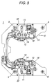
- FIG. 3 is a top view showing a hand base according to the invention.
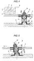
- FIG. 4 is a side view showing a rocking mechanism of the hand according to the invention.
- FIG. 5 is a side view showing an action of the rocking mechanism of the hand according to the invention.
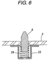
- FIG. 6 is a sectional side view showing a structure of a guide pin according to the invention.
- FIG. 1 is a plan view showing a hand 1 according to the invention.
- a substrate 2 is mounted on the hand 1 .
- the hand 1 serves to mount the substrate 2 thereon in such a manner that a plane of the substrate 2 is horizontal.
- a holding mechanism 7 for directly transmitting/receiving the substrate 2 to/from the hand 1 in a normal direction of the plane of the substrate 2 is drawn in a two-dotted chain line above the hand 1 .
- FIG. 2 is a side view of FIG. 1 , illustrating a part of the holding mechanism 7 .
- the hand 1 is constituted by a rocking hand 3 and a hand base 4 which have the same shapes as seen on a plane, and the hand base 4 is disposed to be superposed on the rocking hand 3 .
- a rocking mechanism 5 which will be described below is provided between the rocking hand 3 and the hand base 4 .
- the rocking hand 3 is supported to be tiltable or movable in parallel with respect to a surface of the hand base 4 .
- the holding mechanism 7 serves to adsorb and hold a surface (an upper surface) of the substrate 2 through an adsorbing surface 8 and to then rotate the substrate 2 about a ⁇ axis in the drawing.
- the three pads 6 are fixed to an upper surface of the rocking hand 3 .
- the three pads 6 take an L shape respectively and have vertical surfaces and almost planes.
- the vertical surfaces take arcuate shapes to draw a part of a circle as shown in FIG. 1 .
- inclined surfaces are formed on respective upper ends of the vertical surfaces.
- the substrate 2 is mounted on the almost plane portion.
- the vertical surfaces of the pads 6 are formed to conform to outer peripheral shapes of the hand 1 according to the invention and the holding mechanism 7 for directly transmitting/receiving the substrate 2 as shown in FIG. 1 .
- the holding mechanism 7 takes the outer peripheral shape of a cylinder. Therefore, the configuration is obtained.
- FIG. 6 shows a more detailed structure of the guide pin 9 .
- FIG. 6 is a sectional view showing the structure of the guide pin 9 .
- the guide pin 9 is supported by a holder 23 and a coil spring 24 .
- the holder 23 envelops the coil spring 24 and is fixed to a back face of the rocking hand 3 .
- a base end side of the guide pin 9 is inserted into a tip of the coil spring 24 and the guide pin 9 is inserted into a through hole provided on the rocking hand 3 and has a tip constituted to be protruded from the surface of the rocking hand 3 .
- the guide pin 9 can be pressed down to a bottom by means of the holding mechanism 7 so as not to disturb the transmission/receipt of the substrate 2 through at least the holding mechanism 7 and the hand 1 .
- two gripping clicks 10 are disposed on the upper surface of the rocking hand 3 .
- the gripping click 10 can grip the outer periphery of the substrate 2 mounted on the pad 6 by means of the two gripping clicks 10 .
- the gripping click 10 can prevent the substrate 2 from being separated from the pad 6 .
- the gripping click 10 is driven by a gripping click driving mechanism 11 provided between the rocking hand 3 and the hand base 4 .
- FIG. 3 is a perspective view showing the rocking hand 3 in the same plan view illustrating the hand 1 according to the invention as FIG. 1 .
- each of the gripping click driving mechanisms 11 for driving the gripping click 10 is constituted by an air cylinder 12 , a sensor 14 and a linear guide 13 .
- the air cylinder 12 can be moved by a proper supply of compressed air through a solenoid valve which is not shown.
- the gripping click 10 is connected to an output shaft of the air cylinder 12 and is operated by means of the air cylinder 12 .
- the gripping click 10 is also connected to the linear guide 13 and can be thus operated with fine guiding in a desirable direction.
- a part of the gripping click 10 is formed to enable light shielding for an optical axis of the sensor 14 and a signal of the sensor 14 is switched depending on an operating position of the gripping click 10 .
- the signal of the sensor 14 is transmitted to a controller of the substrate delivering device which is not shown and detects a state in which the hand 1 accurately grips the substrate 2 or not.
- FIG. 4 is a side view showing a structure of the rocking mechanism 5 in detail.
- the rocking mechanism 5 is mainly constituted by a first spring receiver 15 , a second spring receiver 16 , a compression spring 17 and a shaft 18 .
- a bottom face of the first spring receiver 15 is fixed to an upper surface of the hand base 4 .
- a protrusion is formed on an upper surface of the first spring receiver 15 . The protruded portion is inserted into a base end side of the compression spring 17 .
- An upper surface of the second spring receiver 16 is fixed into a corresponding position to the first spring receiver 15 over the back face of the rocking hand 3 .
- the same projection as that of the first spring receiver 15 is formed on a bottom face of the second spring receiver 16 and is inserted into an upper end side of the compression spring 17 .
- a bowl hole 20 is formed on a center of the first spring receiver 15 from a bottom face. The bowl hole 20 penetrates the upper surface of the first spring receiver 15 .
- the shaft 18 is inserted through the bowl hole 20 .
- a taper portion 19 is formed on a base end side of the shaft 18 and the taper portion 19 and an inclined surface of the bowl hole 20 come in contact with each other.
- a through hole is vertically formed also on a center of the second spring receiver 16 and the shaft 18 penetrates therethrough.
- a tip side of the shaft 18 further penetrates the hand base 4 .
- a nut seat 25 is fixed into corresponding positions to the first spring receiver 15 and the second spring receiver 16 over the upper surface of the rocking hand 3 .
- the same hole as the bowl hole 20 formed on the first spring receiver 15 is provided in the vicinity of a center of the nut seat 25 .
- a screw groove is formed in the vicinity of the tip of the shaft 18 and a nut 21 is engaged therewith.
- the same inclined surface as the taper portion 19 formed on the base end side of the shaft 18 is provided in the vicinity of a lower end of the nut 21 , and the taper portion 19 and the inclined surface of the bowl hole 20 for the shaft 18 come in contact with each other.
- the nut 21 By adjusting the nut 21 , it is possible to regulate a distance between the rocking hand 3 and the hand base 4 . Since the bowl hole 20 abuts on the nut 21 , the nut seat 25 is provided as a separate component from the rocking hand 3 and a material having a high hardness is used in the embodiment. However, it is also possible to directly form the bowl hole 20 on the rocking hand 3 without using the nut seat 25 .
- the rocking hand 3 fixed to be interposed between the nut 21 on the tip of the shaft 18 and the second spring receiver 16 is usually energized apart from the hand base 4 by a spring force of the compression spring 17 .
- the shaft 18 and the taper portion 19 of the nut 21 are provided in contact with the first spring receiver 15 and the bowl hole 20 of the nut seat 25 , they are always stabilized in a guiding state in the normal direction of the rocking hand 3 .
- the hand base 4 When an external force is applied to the hand base 4 , however, the base end side of the shaft 18 is slid in the bowl hole 20 and the taper portion 19 so that the tip side of the shaft 18 (the hand base 4 side) can carry out a precession. Therefore, the hand base 4 is slid in parallel with the rocking hand 3 or is inclined to the rocking hand 3 as shown in FIG. 5 .
- the vertical surface of the pad 6 can first come in contact with the outer periphery of the holding mechanism 7 to move a planar position of the rocking hand 3 in a very small amount with respect to the hand base 4 , thereby carrying out an adjustment even if positions in the planes are shifted from each other or the adsorbing surface 8 is inclined to the hand 1 and horizontal levels are not adapted to each other.
- the rocking hand 3 is inclined to conform to the horizontal level of the adsorbing surface 8 . Therefore, the adsorbing surface 8 and the surface of the substrate 2 are set to be parallel with each other so that the adsorbing surface 8 can reliably adsorb the substrate 2 . More specifically, when the holding mechanism 7 and the hand 1 are to directly transmit/receive the substrate 2 , the direct transmission/receipt can be reliably executed by an action of the rocking mechanism 5 .
- the guide pin 9 guiding the planar position of the substrate 2 in the mounting of the substrate 2 on the hand 1 can be pressed down to the bottom in the rocking hand 3 as shown in FIG. 6 in the embodiment.
- the guide pin 9 is pressed down by the adsorbing surface 8 . Therefore, the transmission/receipt of the substrate 2 through the adsorbing surface 8 and the hand 1 can be prevented from being disturbed.
- an external wall 22 is formed on the hand base 4 to surround the rocking mechanism 5 and the gripping click driving mechanism 11 as shown in FIG. 3 .
- the external wall 22 can prevent water or chemicals from entering the mechanisms from an outside.
Landscapes
- Engineering & Computer Science (AREA)
- Robotics (AREA)
- Mechanical Engineering (AREA)
- Manipulator (AREA)
- Container, Conveyance, Adherence, Positioning, Of Wafer (AREA)
Abstract
Description
Claims (7)
Applications Claiming Priority (2)
| Application Number | Priority Date | Filing Date | Title |
|---|---|---|---|
| JP2008075745A JP5201576B2 (en) | 2008-03-24 | 2008-03-24 | Hand having a swinging mechanism and substrate transport apparatus having the same |
| JPP.2008-075745 | 2008-03-24 |
Publications (2)
| Publication Number | Publication Date |
|---|---|
| US20090236786A1 US20090236786A1 (en) | 2009-09-24 |
| US8038136B2 true US8038136B2 (en) | 2011-10-18 |
Family
ID=41088079
Family Applications (1)
| Application Number | Title | Priority Date | Filing Date |
|---|---|---|---|
| US12/407,826 Active 2030-03-11 US8038136B2 (en) | 2008-03-24 | 2009-03-20 | Hand having rocking mechanism and substrate delivering device having the same |
Country Status (4)
| Country | Link |
|---|---|
| US (1) | US8038136B2 (en) |
| JP (1) | JP5201576B2 (en) |
| KR (1) | KR101201149B1 (en) |
| TW (1) | TWI424911B (en) |
Cited By (2)
| Publication number | Priority date | Publication date | Assignee | Title |
|---|---|---|---|---|
| US20140030047A1 (en) * | 2012-07-30 | 2014-01-30 | Jong-An LEE | Transfer unit of test handler and method of operating the same |
| CN109677928A (en) * | 2019-01-11 | 2019-04-26 | 北京半导体专用设备研究所(中国电子科技集团公司第四十五研究所) | Robot device |
Families Citing this family (7)
| Publication number | Priority date | Publication date | Assignee | Title |
|---|---|---|---|---|
| US10312127B2 (en) | 2013-09-16 | 2019-06-04 | Applied Materials, Inc. | Compliant robot blade for defect reduction |
| CN109719706B (en) * | 2019-01-11 | 2020-10-02 | 北京半导体专用设备研究所(中国电子科技集团公司第四十五研究所) | Substrate unloading manipulator and substrate processing system |
| US11600580B2 (en) * | 2019-02-27 | 2023-03-07 | Applied Materials, Inc. | Replaceable end effector contact pads, end effectors, and maintenance methods |
| US11443973B2 (en) * | 2019-07-12 | 2022-09-13 | Applied Materials, Inc. | Robot for simultaneous substrate transfer |
| KR102268974B1 (en) * | 2019-12-27 | 2021-06-24 | 주식회사 세정로봇 | wafer alignment method of wafer transfer |
| CN114433444B (en) * | 2022-04-11 | 2022-07-01 | 四川上特科技有限公司 | Material containing and transferring device for coating glass powder on wafer |
| JP7730565B2 (en) * | 2022-07-20 | 2025-08-28 | 株式会社スター精機 | Robot Hand |
Citations (13)
| Publication number | Priority date | Publication date | Assignee | Title |
|---|---|---|---|---|
| US6250870B1 (en) * | 1998-08-05 | 2001-06-26 | Micron Electronics, Inc. | Apparatus for handling and processing microelectronic-device substrate assemblies |
| US6462411B1 (en) * | 1997-12-05 | 2002-10-08 | Kokusai Electric Co., Ltd | Semiconductor wafer processing apparatus for transferring a wafer mount |
| US6669434B2 (en) * | 2000-11-17 | 2003-12-30 | Tazmo Co., Ltd. | Double arm substrate transport unit |
| US20040037682A1 (en) * | 2002-08-13 | 2004-02-26 | Junichiro Yoshioka | Substrate holder, plating apparatus, and plating method |
| US20050210669A1 (en) * | 2004-03-29 | 2005-09-29 | Kawasaki Jukogyo Kabushiki Kaisha | Substrate gripping apparatus, substrate gripping method and substrate releasing method |
| US7290813B2 (en) * | 2004-12-16 | 2007-11-06 | Asyst Technologies, Inc. | Active edge grip rest pad |
| US7334826B2 (en) * | 2001-07-13 | 2008-02-26 | Semitool, Inc. | End-effectors for handling microelectronic wafers |
| US7374391B2 (en) * | 2005-12-22 | 2008-05-20 | Applied Materials, Inc. | Substrate gripper for a substrate handling robot |
| US20080156357A1 (en) * | 2006-12-27 | 2008-07-03 | Ichiro Mitsuyoshi | Substrate processing apparatus |
| US20080237172A1 (en) * | 2007-03-30 | 2008-10-02 | Daihen Corporation | Transfer apparatus |
| US20090092469A1 (en) * | 2005-08-29 | 2009-04-09 | Ebara Corporation | Substrate processing unit, substrate transfer method, substrate cleansing process unit, and substrate plating apparatus |
| US7644968B2 (en) * | 2004-01-23 | 2010-01-12 | Kawasaki Jukogyo Kabushiki Kaisha | Substrate holding device |
| US7712806B2 (en) * | 2001-11-13 | 2010-05-11 | Dainippon Screen Mfg. Co., Ltd. | Thin film forming apparatus, film supplier, film cassette, transport mechanism and transport method |
Family Cites Families (8)
| Publication number | Priority date | Publication date | Assignee | Title |
|---|---|---|---|---|
| US4813732A (en) * | 1985-03-07 | 1989-03-21 | Epsilon Technology, Inc. | Apparatus and method for automated wafer handling |
| JPH0429387U (en) * | 1990-06-30 | 1992-03-09 | ||
| JPH04340249A (en) * | 1991-05-17 | 1992-11-26 | Fuji Electric Co Ltd | Semiconductor-wafer treatment apparatus |
| JP2975822B2 (en) * | 1993-11-08 | 1999-11-10 | 三洋電機株式会社 | Robot hand |
| JP2000260846A (en) * | 1999-03-12 | 2000-09-22 | Kokusai Electric Co Ltd | Semiconductor manufacturing equipment |
| TW550151B (en) * | 2001-07-13 | 2003-09-01 | Brooks Automation Inc | Substrate transport apparatus with multiple independent end effectors |
| JP3929364B2 (en) * | 2002-06-26 | 2007-06-13 | エスペック株式会社 | Substrate support and loading / unloading device |
| JP2005230941A (en) * | 2004-02-18 | 2005-09-02 | Sankyo Seiki Mfg Co Ltd | Glass substrate transfer robot |
-
2008
- 2008-03-24 JP JP2008075745A patent/JP5201576B2/en active Active
-
2009
- 2009-03-20 US US12/407,826 patent/US8038136B2/en active Active
- 2009-03-23 TW TW098109371A patent/TWI424911B/en active
- 2009-03-24 KR KR1020090024942A patent/KR101201149B1/en active Active
Patent Citations (14)
| Publication number | Priority date | Publication date | Assignee | Title |
|---|---|---|---|---|
| US6462411B1 (en) * | 1997-12-05 | 2002-10-08 | Kokusai Electric Co., Ltd | Semiconductor wafer processing apparatus for transferring a wafer mount |
| US6250870B1 (en) * | 1998-08-05 | 2001-06-26 | Micron Electronics, Inc. | Apparatus for handling and processing microelectronic-device substrate assemblies |
| US6669434B2 (en) * | 2000-11-17 | 2003-12-30 | Tazmo Co., Ltd. | Double arm substrate transport unit |
| US7334826B2 (en) * | 2001-07-13 | 2008-02-26 | Semitool, Inc. | End-effectors for handling microelectronic wafers |
| US7712806B2 (en) * | 2001-11-13 | 2010-05-11 | Dainippon Screen Mfg. Co., Ltd. | Thin film forming apparatus, film supplier, film cassette, transport mechanism and transport method |
| US20040037682A1 (en) * | 2002-08-13 | 2004-02-26 | Junichiro Yoshioka | Substrate holder, plating apparatus, and plating method |
| US7644968B2 (en) * | 2004-01-23 | 2010-01-12 | Kawasaki Jukogyo Kabushiki Kaisha | Substrate holding device |
| US7547053B2 (en) * | 2004-03-29 | 2009-06-16 | Kawasaki Jukogyo Kabushiki Kaisha | Substrate gripping apparatus, substrate gripping method and substrate releasing method |
| US20050210669A1 (en) * | 2004-03-29 | 2005-09-29 | Kawasaki Jukogyo Kabushiki Kaisha | Substrate gripping apparatus, substrate gripping method and substrate releasing method |
| US7290813B2 (en) * | 2004-12-16 | 2007-11-06 | Asyst Technologies, Inc. | Active edge grip rest pad |
| US20090092469A1 (en) * | 2005-08-29 | 2009-04-09 | Ebara Corporation | Substrate processing unit, substrate transfer method, substrate cleansing process unit, and substrate plating apparatus |
| US7374391B2 (en) * | 2005-12-22 | 2008-05-20 | Applied Materials, Inc. | Substrate gripper for a substrate handling robot |
| US20080156357A1 (en) * | 2006-12-27 | 2008-07-03 | Ichiro Mitsuyoshi | Substrate processing apparatus |
| US20080237172A1 (en) * | 2007-03-30 | 2008-10-02 | Daihen Corporation | Transfer apparatus |
Cited By (6)
| Publication number | Priority date | Publication date | Assignee | Title |
|---|---|---|---|---|
| US20140030047A1 (en) * | 2012-07-30 | 2014-01-30 | Jong-An LEE | Transfer unit of test handler and method of operating the same |
| KR20140017090A (en) * | 2012-07-30 | 2014-02-11 | 삼성전자주식회사 | Transfer unit of test handler and method of operating the same |
| US9573235B2 (en) * | 2012-07-30 | 2017-02-21 | Samsung Electronics Co., Ltd. | Transfer unit of test handler and method of operating the same |
| KR101990973B1 (en) | 2012-07-30 | 2019-06-19 | 삼성전자 주식회사 | Transfer unit of test handler and method of operating the same |
| US10471606B2 (en) * | 2012-07-30 | 2019-11-12 | Samsung Electronics Co., Ltd. | Transfer unit of test handler and method of operating the same |
| CN109677928A (en) * | 2019-01-11 | 2019-04-26 | 北京半导体专用设备研究所(中国电子科技集团公司第四十五研究所) | Robot device |
Also Published As
| Publication number | Publication date |
|---|---|
| KR20090101858A (en) | 2009-09-29 |
| KR101201149B1 (en) | 2012-11-13 |
| JP5201576B2 (en) | 2013-06-05 |
| TWI424911B (en) | 2014-02-01 |
| JP2009226550A (en) | 2009-10-08 |
| US20090236786A1 (en) | 2009-09-24 |
| TW201000274A (en) | 2010-01-01 |
Similar Documents
| Publication | Publication Date | Title |
|---|---|---|
| US8038136B2 (en) | Hand having rocking mechanism and substrate delivering device having the same | |
| US9696369B2 (en) | Wafer test apparatus | |
| KR101638996B1 (en) | The moving apparatus of semiconductor package | |
| KR100664777B1 (en) | Parts mounting device and parts mounting method | |
| US5543890A (en) | Process and device for adjusting the distance between a workpiece and a mask | |
| JP2011165960A (en) | Test head, and semiconductor wafer test device equipped with the same | |
| CN106253049A (en) | The chip adsorbing mechanism of Laser Devices full-automatic eutectic chip mounter | |
| KR20170141114A (en) | Peeling apparatus | |
| JP2018142615A (en) | Wafer transfer holding device | |
| US6921457B2 (en) | Semiconductor manufacturing apparatus, and positioning jig used for same | |
| JP5655017B2 (en) | Work suction and fixing device and ultrasonic inspection system | |
| CN109202941B (en) | Hand of industrial robot and industrial robot | |
| CN110757368A (en) | Alignment device | |
| KR20150073389A (en) | Apparatus for polishing an edge of wafer | |
| CN207587705U (en) | Substrate board treatment | |
| US20040005812A1 (en) | Interface apparatus for reception and delivery of an integrated circuit package from one location to another | |
| CN111492254B (en) | Substrate inspection equipment | |
| CN108431944B (en) | Substrate adsorption device and workbench | |
| JP5097959B2 (en) | Chuck mechanism, transfer device, and frequency adjustment device | |
| KR20080090616A (en) | Wafer support unit and chemical mechanical polishing apparatus having the same | |
| KR101750625B1 (en) | Apparatus for attaching a panel and method using thereof | |
| JP2002151890A (en) | Electronic component mounting equipment | |
| JP2017118063A (en) | Work table with substrate suction device | |
| KR20260056436A (en) | Apparatus for mounting a chip | |
| JP2007142239A (en) | Substrate-holding apparatus |
Legal Events
| Date | Code | Title | Description |
|---|---|---|---|
| AS | Assignment |
Owner name: KABUSHIKI KAISHA YASKAWA DENKI, JAPAN Free format text: ASSIGNMENT OF ASSIGNORS INTEREST;ASSIGNORS:SANEMASA, HIROKI;YAMAMOTO, HIDEO;TORII, NAOOMI;AND OTHERS;REEL/FRAME:022580/0597;SIGNING DATES FROM 20090316 TO 20090325 Owner name: EBARA CORPORATION, JAPAN Free format text: ASSIGNMENT OF ASSIGNORS INTEREST;ASSIGNORS:SANEMASA, HIROKI;YAMAMOTO, HIDEO;TORII, NAOOMI;AND OTHERS;REEL/FRAME:022580/0597;SIGNING DATES FROM 20090316 TO 20090325 Owner name: KABUSHIKI KAISHA YASKAWA DENKI, JAPAN Free format text: ASSIGNMENT OF ASSIGNORS INTEREST;ASSIGNORS:SANEMASA, HIROKI;YAMAMOTO, HIDEO;TORII, NAOOMI;AND OTHERS;SIGNING DATES FROM 20090316 TO 20090325;REEL/FRAME:022580/0597 Owner name: EBARA CORPORATION, JAPAN Free format text: ASSIGNMENT OF ASSIGNORS INTEREST;ASSIGNORS:SANEMASA, HIROKI;YAMAMOTO, HIDEO;TORII, NAOOMI;AND OTHERS;SIGNING DATES FROM 20090316 TO 20090325;REEL/FRAME:022580/0597 |
|
| AS | Assignment |
Owner name: KABUSHIKI KAISHA YASKAWA DENKI, JAPAN Free format text: CORRECTIVE ASSIGNMENT TO CORRECT THE THE THIRD ASSIGNOR'S FIRST NAME TO "HIROOMI". PREVIOUSLY RECORDED ON REEL 022580 FRAME 0597. ASSIGNOR(S) HEREBY CONFIRMS THE ASSIGNMENT;ASSIGNORS:SANEMASA, HIROKI;YAMAMOTO, HIDEO;TORII, HIROOMI;AND OTHERS;SIGNING DATES FROM 20090316 TO 20090325;REEL/FRAME:026907/0046 Owner name: EBARA CORPORATION, JAPAN Free format text: CORRECTIVE ASSIGNMENT TO CORRECT THE THE THIRD ASSIGNOR'S FIRST NAME TO "HIROOMI". PREVIOUSLY RECORDED ON REEL 022580 FRAME 0597. ASSIGNOR(S) HEREBY CONFIRMS THE ASSIGNMENT;ASSIGNORS:SANEMASA, HIROKI;YAMAMOTO, HIDEO;TORII, HIROOMI;AND OTHERS;SIGNING DATES FROM 20090316 TO 20090325;REEL/FRAME:026907/0046 |
|
| STCF | Information on status: patent grant |
Free format text: PATENTED CASE |
|
| FPAY | Fee payment |
Year of fee payment: 4 |
|
| MAFP | Maintenance fee payment |
Free format text: PAYMENT OF MAINTENANCE FEE, 8TH YEAR, LARGE ENTITY (ORIGINAL EVENT CODE: M1552); ENTITY STATUS OF PATENT OWNER: LARGE ENTITY Year of fee payment: 8 |
|
| MAFP | Maintenance fee payment |
Free format text: PAYMENT OF MAINTENANCE FEE, 12TH YEAR, LARGE ENTITY (ORIGINAL EVENT CODE: M1553); ENTITY STATUS OF PATENT OWNER: LARGE ENTITY Year of fee payment: 12 |