US8035460B2 - Surface acoustic wave device, surface acoustic wave filter and antenna duplexer using the same, and electronic equipment using the same - Google Patents
Surface acoustic wave device, surface acoustic wave filter and antenna duplexer using the same, and electronic equipment using the same Download PDFInfo
- Publication number
- US8035460B2 US8035460B2 US12/279,631 US27963107A US8035460B2 US 8035460 B2 US8035460 B2 US 8035460B2 US 27963107 A US27963107 A US 27963107A US 8035460 B2 US8035460 B2 US 8035460B2
- Authority
- US
- United States
- Prior art keywords
- acoustic wave
- surface acoustic
- substrate
- electrode
- idt
- Prior art date
- Legal status (The legal status is an assumption and is not a legal conclusion. Google has not performed a legal analysis and makes no representation as to the accuracy of the status listed.)
- Active, expires
Links
- 238000010897 surface acoustic wave method Methods 0.000 title claims abstract description 61
- 239000000758 substrate Substances 0.000 claims abstract description 100
- 230000001681 protective effect Effects 0.000 claims abstract description 76
- GQYHUHYESMUTHG-UHFFFAOYSA-N lithium niobate Chemical compound [Li+].[O-][Nb](=O)=O GQYHUHYESMUTHG-UHFFFAOYSA-N 0.000 claims abstract description 12
- VYPSYNLAJGMNEJ-UHFFFAOYSA-N Silicium dioxide Chemical compound O=[Si]=O VYPSYNLAJGMNEJ-UHFFFAOYSA-N 0.000 claims description 83
- 239000000377 silicon dioxide Substances 0.000 claims description 41
- 229910052782 aluminium Inorganic materials 0.000 claims description 23
- XAGFODPZIPBFFR-UHFFFAOYSA-N aluminium Chemical compound [Al] XAGFODPZIPBFFR-UHFFFAOYSA-N 0.000 claims description 23
- 238000000034 method Methods 0.000 claims description 20
- 239000000463 material Substances 0.000 claims description 18
- 238000004519 manufacturing process Methods 0.000 claims description 16
- XUIMIQQOPSSXEZ-UHFFFAOYSA-N Silicon Chemical compound [Si] XUIMIQQOPSSXEZ-UHFFFAOYSA-N 0.000 claims description 11
- 229910052751 metal Inorganic materials 0.000 claims description 11
- 239000002184 metal Substances 0.000 claims description 11
- 229910052710 silicon Inorganic materials 0.000 claims description 11
- 239000010703 silicon Substances 0.000 claims description 11
- 238000004544 sputter deposition Methods 0.000 claims description 10
- 229910045601 alloy Inorganic materials 0.000 claims description 8
- 239000000956 alloy Substances 0.000 claims description 8
- 235000012239 silicon dioxide Nutrition 0.000 claims description 2
- CMTSCLKCQBPLSH-UHFFFAOYSA-N isoindole-1,3-dithione Chemical compound C1=CC=C2C(=S)NC(=S)C2=C1 CMTSCLKCQBPLSH-UHFFFAOYSA-N 0.000 description 58
- 229910052681 coesite Inorganic materials 0.000 description 39
- 229910052906 cristobalite Inorganic materials 0.000 description 39
- 229910052682 stishovite Inorganic materials 0.000 description 39
- 229910052905 tridymite Inorganic materials 0.000 description 39
- 230000000052 comparative effect Effects 0.000 description 29
- 239000011295 pitch Substances 0.000 description 16
- 230000008878 coupling Effects 0.000 description 14
- 238000010168 coupling process Methods 0.000 description 14
- 238000005859 coupling reaction Methods 0.000 description 14
- 230000000694 effects Effects 0.000 description 7
- 229910000838 Al alloy Inorganic materials 0.000 description 6
- 239000003989 dielectric material Substances 0.000 description 5
- 238000003780 insertion Methods 0.000 description 5
- 230000037431 insertion Effects 0.000 description 5
- 238000010586 diagram Methods 0.000 description 4
- 229910052802 copper Inorganic materials 0.000 description 3
- 229910052737 gold Inorganic materials 0.000 description 3
- 229910052814 silicon oxide Inorganic materials 0.000 description 3
- 229910052709 silver Inorganic materials 0.000 description 3
- 229910052719 titanium Inorganic materials 0.000 description 3
- 229910052721 tungsten Inorganic materials 0.000 description 3
- 229910004541 SiN Inorganic materials 0.000 description 2
- 229910003069 TeO2 Inorganic materials 0.000 description 2
- 238000006073 displacement reaction Methods 0.000 description 2
- 238000001312 dry etching Methods 0.000 description 2
- 238000005516 engineering process Methods 0.000 description 2
- PBCFLUZVCVVTBY-UHFFFAOYSA-N tantalum pentoxide Inorganic materials O=[Ta](=O)O[Ta](=O)=O PBCFLUZVCVVTBY-UHFFFAOYSA-N 0.000 description 2
- LAJZODKXOMJMPK-UHFFFAOYSA-N tellurium dioxide Chemical compound O=[Te]=O LAJZODKXOMJMPK-UHFFFAOYSA-N 0.000 description 2
- 238000007740 vapor deposition Methods 0.000 description 2
- WSMQKESQZFQMFW-UHFFFAOYSA-N 5-methyl-pyrazole-3-carboxylic acid Chemical compound CC1=CC(C(O)=O)=NN1 WSMQKESQZFQMFW-UHFFFAOYSA-N 0.000 description 1
- OKTJSMMVPCPJKN-UHFFFAOYSA-N Carbon Chemical compound [C] OKTJSMMVPCPJKN-UHFFFAOYSA-N 0.000 description 1
- 229910003327 LiNbO3 Inorganic materials 0.000 description 1
- 239000000853 adhesive Substances 0.000 description 1
- 230000015572 biosynthetic process Effects 0.000 description 1
- 229910052799 carbon Inorganic materials 0.000 description 1
- 239000000919 ceramic Substances 0.000 description 1
- 239000011521 glass Substances 0.000 description 1
- 229910001385 heavy metal Inorganic materials 0.000 description 1
- 238000010884 ion-beam technique Methods 0.000 description 1
- 238000010030 laminating Methods 0.000 description 1
- 238000003475 lamination Methods 0.000 description 1
- 238000010295 mobile communication Methods 0.000 description 1
- 230000000704 physical effect Effects 0.000 description 1
- 229910052594 sapphire Inorganic materials 0.000 description 1
- 239000010980 sapphire Substances 0.000 description 1
- 238000007789 sealing Methods 0.000 description 1
Images


Classifications
-
- H—ELECTRICITY
- H03—ELECTRONIC CIRCUITRY
- H03H—IMPEDANCE NETWORKS, e.g. RESONANT CIRCUITS; RESONATORS
- H03H9/00—Networks comprising electromechanical or electro-acoustic devices; Electromechanical resonators
- H03H9/02—Details
- H03H9/125—Driving means, e.g. electrodes, coils
- H03H9/145—Driving means, e.g. electrodes, coils for networks using surface acoustic waves
- H03H9/14538—Formation
-
- H—ELECTRICITY
- H03—ELECTRONIC CIRCUITRY
- H03H—IMPEDANCE NETWORKS, e.g. RESONANT CIRCUITS; RESONATORS
- H03H9/00—Networks comprising electromechanical or electro-acoustic devices; Electromechanical resonators
- H03H9/25—Constructional features of resonators using surface acoustic waves
-
- H—ELECTRICITY
- H03—ELECTRONIC CIRCUITRY
- H03H—IMPEDANCE NETWORKS, e.g. RESONANT CIRCUITS; RESONATORS
- H03H3/00—Apparatus or processes specially adapted for the manufacture of impedance networks, resonating circuits, resonators
- H03H3/007—Apparatus or processes specially adapted for the manufacture of impedance networks, resonating circuits, resonators for the manufacture of electromechanical resonators or networks
- H03H3/08—Apparatus or processes specially adapted for the manufacture of impedance networks, resonating circuits, resonators for the manufacture of electromechanical resonators or networks for the manufacture of resonators or networks using surface acoustic waves
-
- H—ELECTRICITY
- H03—ELECTRONIC CIRCUITRY
- H03H—IMPEDANCE NETWORKS, e.g. RESONANT CIRCUITS; RESONATORS
- H03H9/00—Networks comprising electromechanical or electro-acoustic devices; Electromechanical resonators
- H03H9/46—Filters
- H03H9/64—Filters using surface acoustic waves
- H03H9/6423—Means for obtaining a particular transfer characteristic
- H03H9/6433—Coupled resonator filters
- H03H9/6483—Ladder SAW filters
-
- H—ELECTRICITY
- H03—ELECTRONIC CIRCUITRY
- H03H—IMPEDANCE NETWORKS, e.g. RESONANT CIRCUITS; RESONATORS
- H03H9/00—Networks comprising electromechanical or electro-acoustic devices; Electromechanical resonators
- H03H9/02—Details
- H03H9/125—Driving means, e.g. electrodes, coils
- H03H9/145—Driving means, e.g. electrodes, coils for networks using surface acoustic waves
- H03H9/14517—Means for weighting
- H03H9/1452—Means for weighting by finger overlap length, apodisation
-
- Y—GENERAL TAGGING OF NEW TECHNOLOGICAL DEVELOPMENTS; GENERAL TAGGING OF CROSS-SECTIONAL TECHNOLOGIES SPANNING OVER SEVERAL SECTIONS OF THE IPC; TECHNICAL SUBJECTS COVERED BY FORMER USPC CROSS-REFERENCE ART COLLECTIONS [XRACs] AND DIGESTS
- Y10—TECHNICAL SUBJECTS COVERED BY FORMER USPC
- Y10T—TECHNICAL SUBJECTS COVERED BY FORMER US CLASSIFICATION
- Y10T29/00—Metal working
- Y10T29/42—Piezoelectric device making
Definitions
- the present invention relates to a surface acoustic wave device used as a resonator or a band-pass filter, and a surface acoustic wave filter and an antenna duplexer using the same, as well as electronic equipment using the same.
- a surface acoustic wave device (hereinafter, referred to as a “SAW device”) is described hereinafter as an example.
- a surface acoustic wave filter formed by using a lithium tantalate (hereinafter, referred to as “LT”) substrate has been widely used.
- LT substrate has a large thermal expansion coefficient of a substrate in the direction in which a surface acoustic wave propagates.
- the elastic constant itself varies according to temperatures. Therefore, there is a problem in terms of the temperature characteristics that the frequency characteristic of a filter is also greatly shifted according to the change in temperatures.
- Japanese Patent Unexamined Publication No. 2004-254291 discloses a method of obtaining a SAW device in which the temperature characteristics is improved.
- the SAW device described in patent document 1 includes a piezoelectric substrate, an electrode film and an insulating film.
- the electrode film is formed on the piezoelectric substrate and constitutes at least one IDT.
- the insulating film is formed by sputtering on the piezoelectric substrate so as to cover the electrode film.
- the insulating film has unevenness on the upper surface thereof.
- the film thickness of the electrode film is in the range from 1-3% of the wavelength of the surface wave to be excited, excellent electrical characteristics can be obtained.
- the present invention obtains an electronic component having excellent temperature characteristics and electrical characteristics.
- a surface acoustic wave device of the present invention includes a substrate including lithium niobate, a IDT, and a protective film.
- the IDT is provided on an upper surface of the substrate and includes a plurality of electrode fingers.
- the protective film covers the IDT and has an uneven shape on an upper surface thereof.
- FIG. 1 is a top view showing a configuration of an electronic component in accordance with a first exemplary embodiment of the present invention.
- FIG. 2 is a partial sectional view showing the electronic component taken along line 2 - 2 of FIG. 1 .
- FIG. 3A is a schematic sectional view to illustrate a method of manufacturing the electronic component of FIG. 1 .
- FIG. 3B is a schematic sectional view to illustrate a method of manufacturing the electronic component of FIG. 1 .
- FIG. 3C is a schematic sectional view to illustrate a method of manufacturing the electronic component of FIG. 1 .
- FIG. 3D a schematic sectional view to illustrate a method of manufacturing the electronic component of FIG. 1 .
- FIG. 3E a schematic sectional view to illustrate a method of manufacturing the electronic component of FIG. 1 .
- FIG. 3F a schematic sectional view to illustrate a method of manufacturing the electronic component of FIG. 1 .
- FIG. 3G a schematic sectional view to illustrate a method of manufacturing the electronic component of FIG. 1 .
- FIG. 3H a schematic sectional view to illustrate a method of manufacturing the electronic component of FIG. 1 .
- FIG. 4 is a sectional view showing an electronic component in a comparative example 3 of the present invention.
- FIG. 5 is a sectional view showing an electronic component in a comparative example 4 of the present invention.
- FIG. 6 is a sectional view showing an electronic component in an example 1 of the present invention.
- FIG. 7 is a graph showing electrical characteristics of the electronic component of FIG. 6 .
- FIG. 8A is a top view showing a configuration of an electronic component in accordance with the first exemplary embodiment of the present invention.
- FIG. 8B is a top view showing a configuration of another electronic component in accordance with the first exemplary embodiment of the present invention.
- FIG. 8C is a schematic configuration view showing a configuration of a further electronic component in accordance with the first exemplary embodiment of the present invention.
- FIG. 9 is a graph showing a temperature coefficient of frequency of the electronic component of FIG. 8A .
- FIG. 10 is a partial sectional view showing a section of another electronic component in accordance with the first exemplary embodiment of the present invention.
- FIG. 11 is a top view showing a main part of an electronic component in accordance with a second exemplary embodiment of the present invention.
- FIG. 12 is a sectional view of the electronic component taken along line 12 - 12 of FIG. 11 .
- FIG. 13 is a partial sectional view showing the electronic component of FIG. 11 .
- FIG. 14 is a characteristic graph showing a relation between an electrode normalized film thickness and a Q value of a resonance point of the electronic component in accordance with the second exemplary embodiment of the present invention.
- FIG. 15 is a characteristic graph showing a relation between a electrode normalized film thickness and a Q value of an anti-resonance point of the electronic component in accordance with the second exemplary embodiment of the present invention.
- FIG. 16 is a characteristic graph showing a passing property of the electronic component in accordance with the second exemplary embodiment of the present invention.
- FIG. 17 is a characteristic graph showing a passing property of the electronic component in accordance with the second exemplary embodiment of the present invention.
- FIG. 18 is a characteristic graph showing a relation between an electrode normalized film thickness and attenuation of the electronic component in accordance with the second exemplary embodiment of the present invention.
- FIG. 19 is a characteristic graph showing a filter property of a ladder-type filter in accordance with the second exemplary embodiment of the present invention.
- FIG. 20 is a characteristic graph showing a filter property of a ladder-type filter in accordance with the second exemplary embodiment of the present invention.
- FIG. 21 is a graph showing a temperature coefficient of frequency of an electronic component in accordance with a third exemplary embodiment of the present invention.
- FIG. 22 is a graph showing an electrical characteristic of an electronic component in accordance with a fourth exemplary embodiment of the present invention.
- FIG. 23 is a graph showing an electrical characteristic of an electronic component in accordance with a fifth exemplary embodiment of the present invention.
- FIG. 24 is a graph showing an electrical characteristic of an electronic component in accordance with a fifth exemplary embodiment of the present invention.
- FIG. 25 is an overview diagram showing electronic equipment in accordance with a sixth exemplary embodiment of the present invention.
- FIG. 26 is an electric circuit diagram showing an inside of the electronic equipment in accordance with the sixth exemplary embodiment of the present invention.
- FIG. 27 is an electrical characteristic graph showing an electrical characteristic of the electronic component in accordance with the sixth exemplary embodiment of the present invention.
- a surface acoustic wave device (hereinafter, referred to as a “SAW device”) is described as an example of an electronic component. Note here that a SAW device has a function as a resonator.
- FIG. 1 is a top view showing a SAW device as an electronic component in accordance with a first exemplary embodiment of the present invention.
- FIG. 2 is a sectional view showing part 23 of the SAW device taken along line 2 - 2 of FIG. 1 .
- surface acoustic wave device 10 in accordance with the first exemplary embodiment includes substrate 1 , IDT 22 , reflector electrode 3 , and protective film 4 .
- IDT 22 is weighted by apodization on an upper surface of substrate 1 , and is provided with predetermined frequency characteristics.
- Reflector electrodes 3 are provided on both sides of IDT 22 .
- Protective film 4 covers at least IDT 22 and reflector electrode 3 .
- IDT 22 has pad 5 that is electrically connected to IDT 22 . IDT 22 takes out an electric signal via pad 5 .
- SAW device 10 is configured.
- Substrate 1 is made of lithium niobate (LiNbO 3 , hereinafter, referred to as “LN”).
- a substrate made of lithium niobate is generally called an LN substrate.
- substrate 1 includes lithium niobate cut out from a Y-plate rotated by D degree around the X-axis in the Z-axis direction. Note here that a 5° Y-LN substrate, in which rotation angle D of the rotation around the X axis in the Z axis direction is 5 degree, is used.
- a pair of IDT 22 and a pair of reflector electrodes 3 are formed on the upper surface of substrate 1 , respectively, and are made of aluminum (hereinafter, referred to as “Al”) or an Al alloy including Al as a main component.
- IDT 22 includes electrode fingers 22 a facing each other with a gap provided between neighboring electrode fingers 22 a.
- protective film 4 is made of silicon oxide such as silicon dioxide (hereinafter, referred to as SiO 2 ). As shown in FIGS. 1 and 2 , protective film 4 has an uneven shape on an upper surface thereof. Convex portion 4 a of protective film 4 is provided above a portion having IDT 22 and reflector electrode 3 on the upper surface of substrate 1 . Concave portion 4 b of protective film 4 is provided in a portion between convex portions 4 a , in which IDT 22 and reflector electrode 3 are not present on the upper surface of substrate 1 and their vicinities.
- a distance between one electrode finger 22 a of one IDT 22 and a portion in which another electrode finger 22 a that is adjacent to the one electrode finer 22 a at one end is located is defined as one pitch width p of IDT 22 .
- the width of one electrode finger 22 a is p 1
- pitch width L of one pitch of protective film 4 and pitch width p of IDT 22 satisfy the relation: L ⁇ p.
- FIG. 2 shows only two electrode fingers 22 a.
- FIGS. 3A to 3H are schematic sectional views to illustrate a method of manufacturing SAW device 10 in accordance with the first exemplary embodiment of the present invention.
- a film of Al or an Al alloy is formed on an upper surface of LN substrate 31 by a method such as vapor deposition and sputtering.
- electrode film 32 is formed.
- electrode film 32 is formed into electrode finger 22 a of IDT 22 or reflector electrode 3 or pad 5 by way of following manufacturing steps.
- LN substrate 31 is shown only partially. However, LN substrate 31 is patterned so that plurality of SAW devices 10 are formed on LN substrate 31 .
- first resist film 33 is formed on an upper surface of electrode film 32 .
- first resist film 33 is processed into predetermined shapes by using an exposure-development technique or the like.
- electrode film 32 is processed into predetermined shapes of electrode finger 22 a of IDT 22 , reflector electrode 3 , or the like, by using a dry-etching technique or the like. Thereafter, first resist film 33 is removed.
- a film of SiO 2 is formed so as to cover electrode film 32 by a method such as vapor deposition or sputtering.
- protective film 34 is formed.
- second resist film 35 is formed on the surface of protective film 34 .
- second resist film 35 is processed into predetermined shapes by using the exposure-development technique or the like.
- unnecessary portions of protective film 34 is removed by using the dry-etching technique or the like, and protective film 4 having opening for pad 5 or the like is formed.
- a plurality of SAW devices 10 formed on LN substrate 31 are divided into individual SAW devices 10 by a method, for example, dicing. Thereafter, SAW device 10 is mounted on a ceramic package by a method, for example, die bonding. Then, SAW device 10 is subjected to wire bonding, and then, a lid is welded to carry out hermetic sealing.
- the shapes and the dimensions of IDT 22 and protective film 4 satisfy the relations: L 1 ⁇ p 1 and L 2 ⁇ p 2 .
- a bias sputtering method is used as a method of obtaining the shapes of IDT 22 and protective film 4 satisfying these relations.
- the bias sputtering method is a method of forming a film by sputtering while applying a bias voltage to electrode film 32 on the side of the substrate in the formation of SiO 2 protective film 34 in FIG. 3E .
- the shape of SiO 2 protective film 34 is controlled by allowing the ratio of the bias voltage applied to electrode film 32 and sputtering electric power to be variable.
- the SiO 2 protective film is formed into leads to obtaining excellent characteristics when protective film 4 is formed, the following four kinds of SAW devices (an example 1 and comparative examples 1 to 4) are formed.
- SAW devices an example 1 and comparative examples 1 to 4
- a SAW device of the comparative example 1 has the electrode normalized film thickness of 4% and is not provided with the SiO 2 protective film.
- a SAW device of the comparative example 2 has the electrode normalized film thickness of 4.5% and is not provided with the SiO 2 protective film.
- a SAW device of the comparative example 3 has the electrode normalized film thickness of 4% and is provided with the SiO 2 protective film whose shape satisfies the relations: L 1 >p 1 and L 2 ⁇ p 2 .
- a SAW device of the comparative example 4 has the electrode normalized film thickness of 4.5% and is provided with the SiO 2 protective film whose shape satisfies the relations: L 1 >p 1 and L 2 ⁇ p 2 .
- SAW device 10 of the example 1 has the electrode normalized film thickness of 4.5% and is provided with the SiO 2 protective film whose shape satisfies the relations: L 1 ⁇ p 1 and L 2 ⁇ p 2 .
- SiO 2 normalized film thickness: t/(2 ⁇ p) in SAW device 10 of the example 1 and the SAW devices of the comparative examples 3 and 4 as mentioned above are all 20%.
- FIG. 4 shows a sectional shape of the SAW device of the comparative example 3
- FIG. 5 shows a sectional shape of the SAW device of the comparative example 4
- FIG. 6 shows a sectional shape of SAW device 10 of the example 1.
- FIG. 7 is a graph showing the electrical characteristics of the SAW devices, respectively.
- Segment line 41 shows the characteristic of the example 1.
- Segment lines 51 , 52 , 53 and 54 show the characteristics of the comparative examples 1, 2, 3, and 4, respectively.
- each SAW device is identified from the results of observation in which the surface of the SAW device is coated with metal and carbon, the electrode is cut by FIB (Focused Ion Beam) in the direction in which the surface acoustic wave propagates, and then observation by the use of an electron microscope is carried out.
- FIB Fluorous Ion Beam
- a SAW device of the comparative example 5 has the electrode normalized film thickness of 3% ⁇ h/(2 ⁇ p) ⁇ 9% and the shape of the SiO 2 protective film satisfying the relations: L 1 >p 1 and L 2 ⁇ p 2 .
- SAW device 10 of the example 2 has the electrode normalized film thickness of 4.5% h/(2 ⁇ p) ⁇ 9% and the shape of the SiO 2 protective film satisfying the relations: L 1 ⁇ p 1 and L 2 ⁇ p 2 .
- 4.5% h/(2 ⁇ p) ⁇ 9% means 0.045 ⁇ h/(2 ⁇ p) 0.09. The same is true in the condition relations mentioned below.
- the SAW device satisfying the conditions of the example 2 is produced as shown in FIG. 8A as an L-type filter in which SAW devices 10 shown in FIG. 1 are connected in serial-parallel arrangement.
- the SAW device satisfying the conditions of the comparative example 5 is produced as shown in FIG. 8A as an L-type filter.
- surface acoustic wave filter 80 (hereinafter, referred to as “filter 80 ”) is formed on substrate 81 made of the LN substrate and includes serially connected surface acoustic wave device 83 (hereinafter, referred to as “SAW device 83 ”) and parallel connected surface acoustic wave device 84 (hereinafter, referred to as “SAW device 84 ”).
- SAW device 10 for at least one of SAW device 83 and SAW device 84 , the effect and advantage of the present invention can be obtained.
- pitch p between the electrodes shown in FIG. 2 is adjusted so that the resonance frequency of SAW device 83 coincides with the anti-resonance frequency of SAW device 84 .
- filter 80 includes input terminal 85 , output terminal 86 , ground terminal 87 and line 88 on substrate 81 .
- SAW device 83 is disposed between input terminal 85 and output terminal 86 .
- Line 88 connects input terminal 85 to SAW device 83 and connects SAW device 83 to output terminal 86 .
- branch point 89 is provided between input terminal 85 and output terminal 86 .
- SAW device 84 is disposed between branch point 89 and ground terminal 87 .
- line 88 connects branch point 89 to SAW device 84 and connects SAW device 84 to ground terminal 87 .
- SAW device 83 and SAW device 84 connected in this way are called serial connection and parallel connection, respectively.
- SAW device 83 and SAW device 84 are covered with protective film 82 .
- FIG. 9 shows the temperature coefficient of frequency (TCF) measured in the center frequency in the filter properties of the SAW devices satisfying the conditions of the comparative example 5 and the example 2.
- line segment 42 shows the temperature coefficient of frequency of the example 2
- line segment 55 shows the temperature coefficient of frequency of the comparative example 5.
- TCF temperature coefficient of frequency
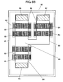
- FIG. 8B is a top view showing a ladder type surface acoustic filter as another electronic component in accordance with the first exemplary embodiment.
- ladder type surface acoustic wave filter 80 includes a plurality of serially connected surface acoustic wave devices 83 and a plurality of parallel connected surface acoustic wave devices 84 on substrate 81 .
- filter 80 includes input terminal 85 , output terminal 86 , ground terminal 87 and line 88 on substrate 81 .
- the plurality of SAW devices 83 are disposed between input terminal 85 and output terminal 86 .
- Line 88 connects input terminal 85 to SAW device 83 , connects SAW device 83 to output terminal 86 , and connects between SAW devices 83 . Furthermore, branch portion 89 is provided between input terminal 85 and output terminal 86 . The plurality of SAW devices 84 are disposed between branch point 89 and ground terminal 87 . Then, line 88 connects branch point 89 to SAW device 84 , connects SAW device 84 to ground terminal 87 , and connects between SAW devices 84 . SAW devices 83 and SAW devices 84 connected in this way are called serial connection and parallel connection, respectively. Furthermore, SAW devices 83 and SAW devices 84 are covered with protective film 82 .
- Filter 80 shown in FIG. 8B includes four SAW devices 83 , two SAW devices 84 and one branch point 89 .
- filter 80 is not limited to this configuration. The combination of SAW device 83 , SAW device 84 and branch point 89 may be determined depending upon characteristics required by filter 80 .
- FIG. 8C is a schematic configuration view showing a longitudinal mode binding type surface acoustic wave filter as another electronic component in accordance with the first exemplary embodiment.
- longitudinal mode binding type surface acoustic wave filter 90 (hereinafter, referred to as “filter 90 ”) includes a plurality of surface acoustic wave devices 10 a (hereinafter, referred to as “SAW devices 10 a ”) disposed along the direction in which the surface acoustic wave propagates (in the direction shown by an arrow 91 ).
- SAW devices 10 a surface acoustic wave devices 10 a
- IDTs 22 constituting neighboring SAW devices 10 a are in adjacent to each other.
- SAW device 10 a includes a pair of IDTs 22 facing each other.
- SAW device 10 a The difference between SAW device 10 a and SAW device 10 is in that individual SAW device 10 a does not include a pair of reflector electrodes 3 respectively but filter 90 as a whole includes a pair of reflector electrodes 3 . Therefore, similar to SAW device 10 , SAW device 10 a has a configuration in which the shape of SiO 2 protective film 4 satisfies the relations: L 1 ⁇ p 1 and L 2 ⁇ p 2 . In addition, SAW device 10 a has the same configuration as SAW device 10 in terms of the conditions such as the electrode normalized film thickness. Thus, also in the configuration of filter 90 , the same effect and advantage as those of SAW device 10 can be exhibited. Note here that filter 90 shown in FIG. 8C includes three SAW devices 10 a .
- filter 90 is not necessarily limited to this configuration.
- a plurality of SAW devices 10 a may be disposed along the direction in which a surface acoustic wave propagates (in the direction shown by arrow 91 ). Furthermore, it is not necessary that SAW device 10 a is used in all the surface acoustic wave devices. At least one surface acoustic wave device may be SAW device 10 a.
- Electrode film 32 In the first exemplary embodiment, Al or an Al alloy is used for electrode film 32 .
- materials of electrode film 32 that is, electrode finger 22 a of IDT 22 and reflector electrode 3 are not limited to these materials.
- a heavy metal having a higher density than Al for example, Ti, Cu, W, Ag, Au, or the like, may be used.
- an ally including a metal having a higher density than Al as a main component may be used.
- electrode film 32 may be formed by laminating first electrode film 32 a and second electrode film 32 b .
- Al or an Al alloy may be used for first electrode film 32 a
- a material having a higher density than Al for example, Ti, Cu, W, Ag, Au, or the like, or an alloy including such materials as a main component
- a material having a higher density than Al for example, Ti, Cu, W, Ag, Au, or the like, or an alloy including such materials as a main component
- Al or an Al alloy may be used for second electrode film 32 b .
- protective film 4 the SiO 2 material is used.
- a material of protective film 4 is not limited to the SiO 2 material.
- other dielectric materials such as SiN, SiON, Ta 2 O 5 , and TeO 2 may be used.
- combinations of such dielectric materials may be used. That is to say, as long as the shape of protective film 4 made of a dielectric material satisfies the conditions of L 1 ⁇ p 1 and L 2 ⁇ p 2 , the same effects can be obtained.
- IDT 22 is weighted by apodization.
- the weighting ratio by apodization is not limited to the configuration shown in FIG. 1 .
- SAW device 10 is a normal type resonator.
- the number of pairs of IDTs 22 and the number of reflector electrodes 3 disposed on both sides of IDT 22 are not limited to those shown in FIG. 1 .
- the ratio of weighting by apodization means a ratio of a region of IDT 22 in which the crossing width of electrode finger 22 a is different from the width of SAW device 10 .
- the bias sputtering method is used as the method of forming protective film 4 .
- the method of forming protective film 4 is not limited to the bias sputtering method. Other methods of forming protective film 4 may be used.
- a SAW device as an electronic component in accordance with a second exemplary embodiment of the present invention is described with reference to drawings.
- FIG. 11 is a top view showing a main part of a SAW device as an electronic component in accordance with the second exemplary embodiment of the present invention.
- FIG. 12 is a sectional view of the SAW device taken along line 12 - 12 of FIG. 11 . Similar to FIG. 12 , FIG. 13 is a sectional view showing the SAW device.
- SAW device 10 includes substrate 1 , IDT 22 , reflector electrode 3 and protective film 4 .
- IDT 22 and reflector electrode 3 are provided on the upper surface of substrate 1 and includes Al or an Al alloy.
- Protective film 4 is made of SiO 2 and covers IDT 22 and reflector electrode 3 . Also, protective film 4 has the uneven shape on the surface thereof.
- substrate 1 is made of lithium niobate cut out from a Y-plate rotated by D degree around the X-axis in the Z-axis direction.
- Rotation angle D satisfies ⁇ 25 degree ⁇ D ⁇ +25 degree, and further preferably, 0 degree ⁇ D ⁇ +25 degree.
- SAW device 10 in accordance with the second exemplary embodiment satisfies the relations: L 1 ⁇ p 1 and L 2 ⁇ p 2 .
- a method of manufacturing SAW device 10 in accordance with the second exemplary embodiment is the same as the method of manufacturing SAW device 10 in accordance with the first exemplary embodiment described with reference to FIGS. 3A to 3H . Therefore, the detailed description is omitted.
- FIG. 14 shows a relation between the electrode normalized film thickness and normalized Qs as a Q value of a resonance point of SAW device 10 in accordance with the second exemplary embodiment of the present invention.
- FIG. 15 shows a relation between the electrode normalized film thickness of SAW device 10 and normalized Qp as a Q value of an anti-resonance point.
- FIGS. 16 and 17 show a passing property of SAW device 10 .
- FIG. 18 shows a relation between the electrode normalized film thickness of SAW device 10 and an attenuation.
- normalized Qs and normalized Qp are normalized by using Qs and Qp when the electrode normalized film thickness is 5.8%.
- protective film 4 uses SiO 2 .
- FIGS. 16 and 17 show the passing property of SAW device 10 .
- FIG. 17 shows the passing property when the electrode normalized film thickness is 8.7%.
- FIG. 16 shows the passing property when the electrode normalized film thickness is 5.8%.
- the attenuation of SAW device 10 when the electrode normalized film thickness is in the range of 7.8% ⁇ h/(2 ⁇ p) ⁇ 9.8% is larger by about 6 dB as compared with the attenuation of SAW device 10 when the electrode normalized film thickness is 5.8%.
- the displacement of the frequency is caused by the difference in the electrode normalized film thickness.
- the configurations of the SAW devices such as the number of pairs, crossing width, or the like, of IDT 22 have the substantially same characteristics.
- the attenuation is larger by about 5 dB or more as compared with the case in which the electrode normalized film thickness is 5.8%.
- the electrode normalized film thickness is in the range of 8.5% ⁇ h/(2 ⁇ p) ⁇ 9.0%, the most excellent property also in terms of the attenuation is exhibited.
- FIGS. 19 and 20 show the filter property of a ladder-type filter in which SAW devices 10 are connected like a ladder.
- An example of the ladder type filter includes a configuration of filter 80 having one stage of serial SAW device 83 and one stage of parallel SAW device 84 , as shown in FIG. 8A .
- FIG. 20 is an enlarged view enlarging part 903 of the filter property shown in FIG. 19 .
- line segment 901 shows the filter property when the electrode normalized film thickness of parallel SAW device 84 is 7.8% and the electrode normalized film thickness of serial SAW device 83 is 8.3%.
- line segment 902 shows the filter property when the electrode normalized film thickness of parallel SAW device 84 is 5.8% and the electrode normalized film thickness of serial SAW device 83 is 6.2%.
- the electrode normalized film thickness is in the range of 7.8% ⁇ h/(2 ⁇ p) ⁇ 9.8%, the insertion loss is improved by 0.1 dB. Note here that the displacement of the frequency is caused by the difference in the electrode normalized film thickness.
- the configurations of the SAW devices such as the number of pairs, crossing width, or the like, of IDT 22 have the substantially same characteristics.
- protective film 4 the SiO 2 material is used.
- a material of protective film 4 is not limited to the SiO 2 material.
- other dielectric materials such as SiN, SiON, Ta 2 O 5 , and TeO 2 may be used.
- combinations of such dielectric materials may be used.
- SAW device 10 constitutes an antenna duplexer as an SAW filter
- pitch p of electrode finger 22 a may be different between a transmitting SAW filter and a receiving SAW filter.
- electrode film thicknesses h are equal to each other, the electrode normalized film thickness h/(2 ⁇ p) becomes different. Therefore, by changing the electrode film thicknesses h of the transmitting SAW filter and the receiving SAW filter, respectively, an antenna duplexer having an optimal configuration can be obtained.
- ladder-type filter 80 as shown in FIG. 8A or FIG. 8B is configured, if the pitch of electrode finger 22 a is different between serial SAW device 83 and parallel SAW device 84 , the electrode normalized film thickness becomes different. In this case, by changing the electrode film thicknesses h in serial SAW device 83 and parallel SAW device 84 , a configuration capable of obtaining optimum filter properties can be realized. Furthermore, the conditions of SAW device 10 as shown in FIG. 8C in the second exemplary embodiment can be applied to a SAW device used in a longitudinal mode binding type surface acoustic wave filter.
- a SAW device as an electronic component in accordance with a third exemplary embodiment of the present invention is described with reference to drawings.
- SAW device 10 in accordance with the third exemplary embodiment SAW device 10 having the same configuration as SAW device 10 used in the first or second exemplary embodiment is used, and filter 80 shown in FIG. 8A is produced. Therefore, since the structure and the manufacturing method of SAW device 10 in the third exemplary embodiment are the same as those of SAW device 10 respectively shown in FIGS. 1 , 2 and 3 , the detail description is omitted.
- FIG. 21 shows a relation between the film thickness of SiO 2 protective film 4 and the temperature coefficient of frequency.
- line segment 40 shows the relation between the film thickness of SiO 2 protective film 4 and the temperature coefficient of frequency.
- SAW device 10 in accordance with the third exemplary embodiment satisfies the relations: L 1 ⁇ p 1 and L 2 ⁇ p 2 .
- the electrode normalized film thickness h/(2 ⁇ p) of IDT 22 is 4.5%.
- a SAW device as an electronic component in accordance with a fourth exemplary embodiment of the present invention is described with reference to drawings.
- SAW device 10 in accordance with the fourth exemplary embodiment uses SAW device 10 having the same configuration as SAW device 10 used in the first or second exemplary embodiment. Therefore, since the structure and the manufacturing method of SAW device 10 are the same as those of SAW device 10 shown in FIGS. 1 , 2 and 3 , the detail description is omitted.
- SAW device 10 satisfies the relations: L 1 ⁇ p 1 and L 2 ⁇ p 2 . Furthermore, in the fourth exemplary embodiment, the electrode normalized film thickness: h/(2 ⁇ p) of IDT 22 used in all examples and comparative examples is 4.5%.
- FIG. 22 shows the relation between the cut-out angle and the electromechanical coupling coefficient.
- values 43 , 44 , and 45 show the electromechanical coupling coefficients of examples 3, 4, 5, respectively.
- values 56 , 57 , and 58 show the electromechanical coupling coefficients of the comparative examples 6, 7, and 8, respectively.
- the examples 3, 4, and 5 show the electromechanical coupling coefficients when D is 5 degree, 15 degree, and ⁇ 5 degree, respectively.
- the comparative examples 6 and 7 show the electromechanical coupling coefficients when D is 41 degree and 64 degree, respectively.
- the comparative example 8 shows the electromechanical coupling coefficient when the SiO 2 protective film is not provided and D is 64 degree.
- the coupling coefficient when the cut-out angle D is 41 degree is about 11% and the coupling coefficient when the cut-out angle D is 64 degree is about 5.5%.
- the examples 3, 4 and 5 extremely large electromechanical coupling coefficients are obtained.
- the electromechanical coupling coefficient when the SiO 2 protective film is not provided and D is 64 degree is shown in the drawing. Therefore, in order to obtain an electromechanical coupling coefficient that is not smaller than the electromechanical coupling coefficient when the SiO 2 protective film is not provided, D satisfies at least the relation: ⁇ 25 degree ⁇ D ⁇ 25 degree.
- SAW device 10 when SAW device 10 is produced so that it satisfies the relations: L 1 ⁇ p 1 and L 2 ⁇ p 2 and the cut-out angle D of the LN substrate satisfies the relation: ⁇ 25 degree ⁇ D ⁇ 25 degree, SAW device 10 having the excellent temperature characteristics and the large electromechanical coupling coefficient can be obtained.
- the cut-out angle D of the LN substrate a rotation angle around the X-axis in the Z-axis direction is defined as D degree.
- a SAW device as an electronic component in accordance with a fifth exemplary embodiment of the present invention is described with reference to drawings.
- the configuration of other than substrate 1 is the same as in SAW device 10 used in the first or second exemplary embodiment.
- a method of bonding the LN substrate and the silicon substrate to each other a method such as a direct bonding technology or a bonding method using an adhesive agent can be used.
- SAW device 10 in accordance with the fifth exemplary embodiment satisfies the relations: L 1 ⁇ p 1 and L 2 ⁇ p 2 .
- two kinds of SAW devices 10 are produced.
- FIGS. 23 and 24 show the electrical characteristics of SAW device 10 measured in the temperature environment of ⁇ 35 degree Celsius, 25 degree Celsius, and +85 degree Celsius, respectively.
- FIG. 23 shows the characteristic as a comparative example 9, when the 5° Y-LN substrate is used as substrate 1 .
- Line segments 59 a , 59 b and 59 c show the electrical characteristics of the SAW device as the comparative example 9 measured in the temperature environment of ⁇ 35 degree Celsius, 25 degree Celsius, and +85 degree Celsius, respectively.
- FIG. 24 shows the characteristic as an example 6 when the bonded substrate of the 5° Y-LN substrate and the silicon substrate is used as substrate 1 .
- line segments 45 a , 45 b and 45 c show the electrical characteristics of SAW device 10 of the example 6 measured in the temperature environment of ⁇ 35 degree Celsius, 25 degree Celsius, and +85 degree Celsius, respectively.
- the frequency variation with respect to temperatures when the bonded substrate of the 5° Y-LN substrate and the silicon substrate is used as substrate 1 is smaller as compared with the frequency variation with respect to temperatures when the 5° Y-LN substrate is used as substrate 1 .
- the temperature coefficient of frequency calculated from the anti-resonant frequency in the respective characteristics is about ⁇ 33 ppm/K when the 5° Y-LN substrate is used as substrate 1 .
- the temperature coefficient of frequency is about ⁇ 10 ppm/K when the bonded substrate of the 5° Y-LN substrate and the silicon substrate is used as substrate 1 , showing a significant improvement. Therefore, when the bonded substrate of the LN substrate and the silicon substrate is used as substrate 1 , it is possible to obtain SAW device 10 having further excellent temperature characteristics and electrical characteristic.
- the fifth exemplary embodiment does not refer to a thickness of the LN substrate, when the LN substrate is polished so as to be thin and then laminated with a silicon substrate, an effect of further improvement of the temperature characteristics can be obtained.
- the silicon substrate is used.
- glass, sapphire, or the like, having smaller coefficient of thermal expansion than the silicon substrate is used, the equal or higher effect can be obtained.
- a mobile phone is described as an example of electronic equipment.
- FIG. 25 is an overview diagram showing a mobile phone in accordance with the sixth exemplary embodiment of the present invention.
- FIG. 26 is an electric-circuit diagram showing a main part stored inside the mobile phone shown in FIG. 25 .
- mobile phone 140 includes first case 141 and second case 142 , which are held around hinge part 143 in a way capable of opening and closing.
- mobile phone 140 has display part 144 and antenna 151 provided on first case 141 , and input part 145 provided on second case 142 .
- a circuit such as radio circuit (not shown) is stored inside first case 141 and second case 142 , respectively.
- mobile phone 140 includes antenna 151 and antenna duplexer 152 connected to antenna 151 .
- Antenna duplexer 152 includes transmitting SAW filter 153 , receiving SAW filter 154 and phase circuit 155 . Transmitting SAW filter 153 and receiving SAW filter 154 are configured by connecting plural stages of SAW devices 10 described in the first to fifth exemplary embodiments in serial-parallel arrangement.
- Antenna duplexer 152 is an electric circuit that is electrically connected to antenna 151 , for example, an antenna duplexer for WCDMA.
- transmitting SAW filter 153 and receiving SAW filter 154 constituting antenna duplexer 152 may have different pitches of electrode finger 22 a .
- transmitting SAW filter 153 and receiving SAW filter 154 may have different electrode normalized film thicknesses respectively, the frequency characteristics can be adjusted.
- electrode film thickness h can be changed between a filter at the transmitting side and a filter at the receiving side, an optimum configuration of antenna duplexer 152 can be obtained.
- FIG. 27 shows the electrical characteristics of antenna duplexer 152 using transmitting SAW filter 153 and receiving SAW filter 154 .
- Line segment 47 shows the electrical characteristic of transmitting SAW filter 153 and line segment 48 shows the electrical characteristic of receiving SAW filter 154 .
- the passband an excellent insertion loss of about ⁇ 1.5 dB is realized.
- the stopband an excellent attenuation of about ⁇ 60 dB is realized.
- the passband means the range from 1920 MHz to 1980 MHz at the transmitting side and the range from 2110 MHz to 2170 MHz at the receiving side.
- the stopband means the range from 2110 MHz to 2170 MHz at the transmitting side and the range from 1920 MHz to 1980 MHz at the receiving side. In this way, when SAW devices 10 described in the first to fifth exemplary embodiments are used in the electronic equipment, it is possible to easily obtain an antenna duplexer that is excellent in the temperature characteristics and the electrical characteristics.
- a protective film is formed so as to cover an electrode formed on a substrate.
- the shape or the thickness of the protective film is set to a specific range, it is possible to obtain a surface acoustic wave device that is excellent in the temperature characteristics and the electrical characteristic.
Landscapes
- Physics & Mathematics (AREA)
- Acoustics & Sound (AREA)
- Engineering & Computer Science (AREA)
- Manufacturing & Machinery (AREA)
- Surface Acoustic Wave Elements And Circuit Networks Thereof (AREA)
Abstract
Description
- [Patent Document 1] Japanese Patent Unexamined Publication No. 2004-254291
- 1 substrate
- 3 reflector electrode
- 4, 34 protective film
- 4 a convex portion
- 4 b concave portion
- 5 pad
- 10, 10 a, 83, 84 surface acoustic wave device
- 22 IDT
- 22 a electrode finger
- 31 LN substrate
- 32 electrode film
- 33 first resist film
- 35 second resist film
- 80 surface acoustic wave filter
- 81 substrate
- 82 protective film
- 85 input terminal
- 86 output terminal
- 87 ground terminal
- 88 line
- 89 branch point
- 90 longitudinal mode binding type surface acoustic wave filter
- 151 antenna
- 152 antenna duplexer
- 153 transmitting SAW filter
- 154 receiving SAW filter
- 155 phase circuit
Claims (21)
p1+p2=p, and 7.8%≦h/(2×p)≦9.8%,
L1+L2=L, L1≦p1, and L2≧p2
8.5%≦h/(2×p)≦9.0%.
p1+p2=p, and 7.8%≦h/(2×p)≦9.8%
L1+L2=L, L1≦p1, and L2≧p2
p1+p2=p, and h/(2×p)≧4.5%,
L1+L2=L, L1≦p1, and L2≧p2
8.5%≦h/(2×p)≦9.0%.
Applications Claiming Priority (5)
| Application Number | Priority Date | Filing Date | Title |
|---|---|---|---|
| JP2006039001A JP5025963B2 (en) | 2006-02-16 | 2006-02-16 | Electronic component, method for manufacturing the same, and electronic device using the electronic component |
| JP2006-039001 | 2006-02-16 | ||
| JP2006-255588 | 2006-09-21 | ||
| JP2006255588A JP4544227B2 (en) | 2006-09-21 | 2006-09-21 | Elastic wave resonator, elastic wave filter and antenna duplexer using the same |
| PCT/JP2007/052631 WO2007094368A1 (en) | 2006-02-16 | 2007-02-14 | Surface acoustic wave device, surface acoustic wave filter employing same and antenna duplexer, and electronic apparatus employing same |
Publications (2)
| Publication Number | Publication Date |
|---|---|
| US20100164646A1 US20100164646A1 (en) | 2010-07-01 |
| US8035460B2 true US8035460B2 (en) | 2011-10-11 |
Family
ID=38371547
Family Applications (1)
| Application Number | Title | Priority Date | Filing Date |
|---|---|---|---|
| US12/279,631 Active 2028-05-01 US8035460B2 (en) | 2006-02-16 | 2007-02-14 | Surface acoustic wave device, surface acoustic wave filter and antenna duplexer using the same, and electronic equipment using the same |
Country Status (4)
| Country | Link |
|---|---|
| US (1) | US8035460B2 (en) |
| EP (1) | EP1971026A1 (en) |
| KR (2) | KR100961481B1 (en) |
| WO (1) | WO2007094368A1 (en) |
Cited By (2)
| Publication number | Priority date | Publication date | Assignee | Title |
|---|---|---|---|---|
| US20110309719A1 (en) * | 2009-03-04 | 2011-12-22 | Murata Manufacturing Co., Ltd. | Surface acoustic wave element and method of manufacturing same |
| US11522515B2 (en) | 2017-03-16 | 2022-12-06 | Skyworks Solutions, Inc. | Acoustic wave device including interdigital electrodes covered by silicon oxynitride film |
Families Citing this family (15)
| Publication number | Priority date | Publication date | Assignee | Title |
|---|---|---|---|---|
| KR100961481B1 (en) | 2006-02-16 | 2010-06-08 | 파나소닉 주식회사 | Surface acoustic wave device, surface acoustic wave filter employing same and antenna duplexer, and electronic apparatus employing same |
| JP4569699B2 (en) * | 2006-12-27 | 2010-10-27 | パナソニック株式会社 | Surface acoustic wave resonator, surface acoustic wave filter and antenna duplexer using the same |
| US8476991B2 (en) * | 2007-11-06 | 2013-07-02 | Panasonic Corporation | Elastic wave resonator, elastic wave filter, and antenna sharing device using the same |
| JP5332506B2 (en) * | 2008-10-28 | 2013-11-06 | 株式会社村田製作所 | Ladder type filter and duplexer having the same |
| WO2010131450A1 (en) | 2009-05-14 | 2010-11-18 | パナソニック株式会社 | Antenna sharing device |
| KR20110020741A (en) * | 2009-08-24 | 2011-03-03 | 엔지케이 인슐레이터 엘티디 | Method for manufacturing composite substrate |
| CN104467729B (en) | 2009-11-02 | 2018-08-03 | 天工滤波方案日本有限公司 | Elastic wave device and its duplexer and electronic equipment for using |
| WO2011102128A1 (en) * | 2010-02-22 | 2011-08-25 | パナソニック株式会社 | Antenna sharing device |
| JP2011182220A (en) * | 2010-03-02 | 2011-09-15 | Panasonic Corp | Acoustic wave resonator and vertically coupled double mode filter using the same, as well as ladder filter |
| WO2012036178A1 (en) * | 2010-09-17 | 2012-03-22 | 株式会社村田製作所 | Acoustic-wave device |
| JP2014504827A (en) * | 2011-01-24 | 2014-02-24 | エプコス アクチエンゲゼルシャフト | Surface acoustic wave filter |
| WO2013002033A1 (en) * | 2011-06-28 | 2013-01-03 | 京セラ株式会社 | Elastic wave element and elastic wave device using same |
| JP5892762B2 (en) * | 2011-10-12 | 2016-03-23 | 太陽誘電株式会社 | Elastic wave device |
| CN106664068B (en) | 2014-07-25 | 2019-06-14 | 株式会社村田制作所 | Bandpass filter and filter module |
| WO2021124806A1 (en) * | 2019-12-20 | 2021-06-24 | 株式会社村田製作所 | Electronic component module and method for manufacturing electronic component module |
Citations (28)
| Publication number | Priority date | Publication date | Assignee | Title |
|---|---|---|---|---|
| JPS63260213A (en) | 1986-09-12 | 1988-10-27 | Hiroshi Shimizu | Resonator using high coupling love wave type saw substrate |
| JPH05267990A (en) | 1991-08-21 | 1993-10-15 | Toyo Commun Equip Co Ltd | Longitudinal coupling double mode saw filter |
| JPH0774586A (en) | 1993-08-31 | 1995-03-17 | Murata Mfg Co Ltd | Surface acoustic wave device |
| US5506552A (en) | 1993-11-05 | 1996-04-09 | Matsushita Electric Industrial Co., Ltd. | Surface acoustic wave filter with multiple ground terminals |
| US5729186A (en) | 1995-04-12 | 1998-03-17 | Matsushita Electric Industrial Co., Ltd. | Resonator ladder surface acoustic wave filter suppressing spurious signals |
| JPH1084245A (en) | 1996-09-10 | 1998-03-31 | Hitachi Ltd | Surface acoustic wave element |
| JPH1155070A (en) | 1997-06-02 | 1999-02-26 | Matsushita Electric Ind Co Ltd | Surface acoustic wave element and its producing method |
| JPH1188100A (en) | 1997-09-03 | 1999-03-30 | Toyo Commun Equip Co Ltd | Surface acoustic wave device |
| US6037847A (en) | 1995-10-13 | 2000-03-14 | Fujitsu Limited | Surface acoustic wave device using a leaky surface acoustic wave with an optimized cut angle of a piezoelectric substrate |
| KR20020071736A (en) | 2001-03-04 | 2002-09-13 | 카즈히코 야마노우치 | Surface acoustic wave substrate and surface acoustic wave functional element |
| JP2002314365A (en) | 2001-04-17 | 2002-10-25 | Hitachi Ltd | Surface acoustic wave resonator having desired bandwidth ratio and method of manufacturing the same |
| US20030080831A1 (en) | 2001-10-25 | 2003-05-01 | Naumenko Natalya F. | Surface acoustic wave devices using optimized cuts of lithium niobate (LiNbO3) |
| JP2003209458A (en) | 2001-03-04 | 2003-07-25 | Kazuhiko Yamanouchi | Surface acoustic wave substrate and surface acoustic wave functional element |
| US20030151329A1 (en) * | 2001-10-12 | 2003-08-14 | Michio Kadota | Surface acoustic wave device |
| JP2004120685A (en) | 2002-09-30 | 2004-04-15 | Fujitsu Media Device Kk | Surface acoustic wave filter, and surface acoustic wave frequency divider having the same |
| WO2004066493A1 (en) | 2003-01-23 | 2004-08-05 | Epcos Ag | Saw component having an improved temperature coefficient |
| JP2004222267A (en) | 2002-12-25 | 2004-08-05 | Matsushita Electric Ind Co Ltd | Electronic component and electronic equipment using the same |
| JP2004254291A (en) | 2003-01-27 | 2004-09-09 | Murata Mfg Co Ltd | Acoustic surface wave device |
| US20040174233A1 (en) | 2002-04-15 | 2004-09-09 | Ryoichi Takayama | Surface acoustic wave device, and mobile communication device and sensor both using same |
| JP2005080202A (en) | 2003-09-03 | 2005-03-24 | Murata Mfg Co Ltd | Surface acoustic wave element |
| WO2005034347A1 (en) * | 2003-10-03 | 2005-04-14 | Murata Manufacturing Co., Ltd. | Surface acoustic wave device |
| KR20050085878A (en) | 2002-12-25 | 2005-08-29 | 마츠시타 덴끼 산교 가부시키가이샤 | Electronic component and electronic apparatus using this electronic component |
| JP2005347892A (en) | 2004-05-31 | 2005-12-15 | Fujitsu Media Device Kk | Surface acoustic wave element |
| JP2005348139A (en) * | 2004-06-03 | 2005-12-15 | Murata Mfg Co Ltd | Elastic wave device and method for manufacturing the same |
| WO2006003933A1 (en) | 2004-06-30 | 2006-01-12 | Matsushita Electric Industrial Co., Ltd. | Electronic part and manufacturing method thereof |
| US20060022768A1 (en) | 2004-07-28 | 2006-02-02 | Kyocera Corporation | Surface acoustic wave device, surface acoustic wave apparatus, and communications equipment |
| WO2006032335A1 (en) | 2004-09-17 | 2006-03-30 | Epcos Ag | Saw-component having a reduced temperature path and method for the production thereof |
| KR20080077193A (en) | 2006-02-16 | 2008-08-21 | 마쯔시다덴기산교 가부시키가이샤 | Surface acoustic wave device, surface acoustic wave filter employing same and antenna duplexer, and electronic apparatus employing same |
-
2007
- 2007-02-14 KR KR1020087014499A patent/KR100961481B1/en active IP Right Grant
- 2007-02-14 EP EP07714184A patent/EP1971026A1/en not_active Withdrawn
- 2007-02-14 WO PCT/JP2007/052631 patent/WO2007094368A1/en active Application Filing
- 2007-02-14 US US12/279,631 patent/US8035460B2/en active Active
- 2007-02-14 KR KR1020107001186A patent/KR100979952B1/en active IP Right Grant
Patent Citations (38)
| Publication number | Priority date | Publication date | Assignee | Title |
|---|---|---|---|---|
| JPS63260213A (en) | 1986-09-12 | 1988-10-27 | Hiroshi Shimizu | Resonator using high coupling love wave type saw substrate |
| JPH05267990A (en) | 1991-08-21 | 1993-10-15 | Toyo Commun Equip Co Ltd | Longitudinal coupling double mode saw filter |
| JPH0774586A (en) | 1993-08-31 | 1995-03-17 | Murata Mfg Co Ltd | Surface acoustic wave device |
| US5506552A (en) | 1993-11-05 | 1996-04-09 | Matsushita Electric Industrial Co., Ltd. | Surface acoustic wave filter with multiple ground terminals |
| US5729186A (en) | 1995-04-12 | 1998-03-17 | Matsushita Electric Industrial Co., Ltd. | Resonator ladder surface acoustic wave filter suppressing spurious signals |
| US6037847A (en) | 1995-10-13 | 2000-03-14 | Fujitsu Limited | Surface acoustic wave device using a leaky surface acoustic wave with an optimized cut angle of a piezoelectric substrate |
| JPH1084245A (en) | 1996-09-10 | 1998-03-31 | Hitachi Ltd | Surface acoustic wave element |
| JPH1155070A (en) | 1997-06-02 | 1999-02-26 | Matsushita Electric Ind Co Ltd | Surface acoustic wave element and its producing method |
| US5998907A (en) | 1997-06-02 | 1999-12-07 | Matsushita Electric Industrial Co., Ltd. | Surface acoustic wave devices and their manufacturing method |
| JPH1188100A (en) | 1997-09-03 | 1999-03-30 | Toyo Commun Equip Co Ltd | Surface acoustic wave device |
| KR20020071736A (en) | 2001-03-04 | 2002-09-13 | 카즈히코 야마노우치 | Surface acoustic wave substrate and surface acoustic wave functional element |
| US20020140316A1 (en) | 2001-03-04 | 2002-10-03 | Kazuhiko Yamanouchi | Surface acoustic wave substrate and surface acoustic wave functional element |
| JP2003209458A (en) | 2001-03-04 | 2003-07-25 | Kazuhiko Yamanouchi | Surface acoustic wave substrate and surface acoustic wave functional element |
| US6791237B2 (en) | 2001-03-04 | 2004-09-14 | Kazuhiko Yamanouchi | Surface acoustic wave substrate and surface acoustic wave functional element |
| JP2002314365A (en) | 2001-04-17 | 2002-10-25 | Hitachi Ltd | Surface acoustic wave resonator having desired bandwidth ratio and method of manufacturing the same |
| US20030151329A1 (en) * | 2001-10-12 | 2003-08-14 | Michio Kadota | Surface acoustic wave device |
| US20030080831A1 (en) | 2001-10-25 | 2003-05-01 | Naumenko Natalya F. | Surface acoustic wave devices using optimized cuts of lithium niobate (LiNbO3) |
| US20040174233A1 (en) | 2002-04-15 | 2004-09-09 | Ryoichi Takayama | Surface acoustic wave device, and mobile communication device and sensor both using same |
| JP2004120685A (en) | 2002-09-30 | 2004-04-15 | Fujitsu Media Device Kk | Surface acoustic wave filter, and surface acoustic wave frequency divider having the same |
| US6975185B2 (en) | 2002-09-30 | 2005-12-13 | Fujitsu Media Devices Ltd. | Surface acoustic wave filter and surface acoustic wave duplexer having the same |
| JP2004222267A (en) | 2002-12-25 | 2004-08-05 | Matsushita Electric Ind Co Ltd | Electronic component and electronic equipment using the same |
| US20060158800A1 (en) | 2002-12-25 | 2006-07-20 | Matsushita Electric Industrial Co., Ltd. | Electronic component and electronic apparatus using this electronic component |
| US7538636B2 (en) | 2002-12-25 | 2009-05-26 | Panasonic Corporation | Electronic part with a comb electrode and protective film and electronic equipment including same |
| KR20050085878A (en) | 2002-12-25 | 2005-08-29 | 마츠시타 덴끼 산교 가부시키가이샤 | Electronic component and electronic apparatus using this electronic component |
| WO2004066493A1 (en) | 2003-01-23 | 2004-08-05 | Epcos Ag | Saw component having an improved temperature coefficient |
| JP2004254291A (en) | 2003-01-27 | 2004-09-09 | Murata Mfg Co Ltd | Acoustic surface wave device |
| US7209018B2 (en) | 2003-01-27 | 2007-04-24 | Murata Manufacturing Co., Ltd. | Surface acoustic wave device |
| JP2005080202A (en) | 2003-09-03 | 2005-03-24 | Murata Mfg Co Ltd | Surface acoustic wave element |
| US20070096592A1 (en) * | 2003-10-03 | 2007-05-03 | Michio Kadota | Surface acoustic wave device |
| WO2005034347A1 (en) * | 2003-10-03 | 2005-04-14 | Murata Manufacturing Co., Ltd. | Surface acoustic wave device |
| JP2005347892A (en) | 2004-05-31 | 2005-12-15 | Fujitsu Media Device Kk | Surface acoustic wave element |
| US7423365B2 (en) | 2004-05-31 | 2008-09-09 | Fujitsu Media Devices Limited | Surface acoustic wave device |
| JP2005348139A (en) * | 2004-06-03 | 2005-12-15 | Murata Mfg Co Ltd | Elastic wave device and method for manufacturing the same |
| WO2006003933A1 (en) | 2004-06-30 | 2006-01-12 | Matsushita Electric Industrial Co., Ltd. | Electronic part and manufacturing method thereof |
| US20060022768A1 (en) | 2004-07-28 | 2006-02-02 | Kyocera Corporation | Surface acoustic wave device, surface acoustic wave apparatus, and communications equipment |
| WO2006032335A1 (en) | 2004-09-17 | 2006-03-30 | Epcos Ag | Saw-component having a reduced temperature path and method for the production thereof |
| KR20080077193A (en) | 2006-02-16 | 2008-08-21 | 마쯔시다덴기산교 가부시키가이샤 | Surface acoustic wave device, surface acoustic wave filter employing same and antenna duplexer, and electronic apparatus employing same |
| EP1971026A1 (en) | 2006-02-16 | 2008-09-17 | Matsushita Electric Industrial Co., Ltd. | Surface acoustic wave device, surface acoustic wave filter employing same and antenna duplexer, and electronic apparatus employing same |
Non-Patent Citations (7)
| Title |
|---|
| English language machine translation of JP 2005-348139 published Dec. 15, 2005. * |
| European Office action for 07 714 184.4-2215 dated Apr. 29, 2011. |
| European Search Report dated Aug. 26, 2009. |
| International Search Report for PCT/JP2007/052631; Mar. 27, 2007. |
| Japanese Office action for Appl. No. JP 2006-039001 dated Mar. 23, 2010. |
| Japanese Office action for Appl. No. JP 2006-255588 dated Mar. 23, 2010. |
| Wright; "A Review fo Saw Resonator Filter Technology", Ultrasonics Symposium-29, 1992, pp. 29-38. |
Cited By (3)
| Publication number | Priority date | Publication date | Assignee | Title |
|---|---|---|---|---|
| US20110309719A1 (en) * | 2009-03-04 | 2011-12-22 | Murata Manufacturing Co., Ltd. | Surface acoustic wave element and method of manufacturing same |
| US8575818B2 (en) * | 2009-03-04 | 2013-11-05 | Murata Manufacturing Co., Ltd. | Surface acoustic wave element |
| US11522515B2 (en) | 2017-03-16 | 2022-12-06 | Skyworks Solutions, Inc. | Acoustic wave device including interdigital electrodes covered by silicon oxynitride film |
Also Published As
| Publication number | Publication date |
|---|---|
| US20100164646A1 (en) | 2010-07-01 |
| KR20080077193A (en) | 2008-08-21 |
| KR100979952B1 (en) | 2010-09-03 |
| WO2007094368A1 (en) | 2007-08-23 |
| EP1971026A1 (en) | 2008-09-17 |
| KR20100023964A (en) | 2010-03-04 |
| KR100961481B1 (en) | 2010-06-08 |
Similar Documents
| Publication | Publication Date | Title |
|---|---|---|
| US8035460B2 (en) | Surface acoustic wave device, surface acoustic wave filter and antenna duplexer using the same, and electronic equipment using the same | |
| US7692515B2 (en) | Low-loss electro-acoustic component | |
| US7659653B2 (en) | Acoustic wave device and filter | |
| KR101516653B1 (en) | Elastic surface wave filter device | |
| US7688161B2 (en) | Acoustic wave device and filter using the same | |
| JP4552931B2 (en) | Elastic wave device, mobile communication device and sensor using the same | |
| JP5025963B2 (en) | Electronic component, method for manufacturing the same, and electronic device using the electronic component | |
| US20060181366A1 (en) | Demultiplexer and surface acoustic wave filter | |
| US7301421B2 (en) | Surface acoustic wave device, manufacturing method therefor, and communications equipment | |
| CN102396154A (en) | Elastic wave element and electronic apparatus using same | |
| WO2005125005A1 (en) | Saw device and apparatus employing it | |
| US10958241B2 (en) | Extractor | |
| US20050127794A1 (en) | Surface acoustic wave device and manufacturing method thereof | |
| JP7278305B2 (en) | Acoustic wave device, branching filter and communication device | |
| EP3776855B1 (en) | Surface acoustic wave device on composite substrate | |
| US10886893B2 (en) | Reduced-size guided-surface acoustic wave (SAW) devices | |
| JP4305173B2 (en) | Electronic component and electronic device using the electronic component | |
| JP4454410B2 (en) | Surface acoustic wave device, method of manufacturing the same, and communication device | |
| JP2001345675A (en) | Surface acoustic wave filter | |
| JP4458954B2 (en) | Surface acoustic wave device, method of manufacturing the same, and communication device | |
| JPWO2002045262A1 (en) | Elastic wave device | |
| JP4454411B2 (en) | Surface acoustic wave device, method of manufacturing the same, and communication device | |
| KR20210029806A (en) | Seismic device, seismic filter and composite filter device | |
| JP2004222266A (en) | Electronic component and electronic equipment using the same | |
| JP2001313538A (en) | Surface acoustic wave device |
Legal Events
| Date | Code | Title | Description |
|---|---|---|---|
| AS | Assignment |
Owner name: MATSUSHITA ELECTRIC INDUSTRIAL CO., LTD.,JAPAN Free format text: ASSIGNMENT OF ASSIGNORS INTEREST;ASSIGNORS:NAKANISHI, HIDEKAZU;TAKAYAMA, RYOICHI;IWASAKI, YUKIO;AND OTHERS;SIGNING DATES FROM 20080623 TO 20080624;REEL/FRAME:021481/0874 Owner name: MATSUSHITA ELECTRIC INDUSTRIAL CO., LTD., JAPAN Free format text: ASSIGNMENT OF ASSIGNORS INTEREST;ASSIGNORS:NAKANISHI, HIDEKAZU;TAKAYAMA, RYOICHI;IWASAKI, YUKIO;AND OTHERS;SIGNING DATES FROM 20080623 TO 20080624;REEL/FRAME:021481/0874 |
|
| AS | Assignment |
Owner name: PANASONIC CORPORATION,JAPAN Free format text: CHANGE OF NAME;ASSIGNOR:MATSUSHITA ELECTRIC INDUSTRIAL CO., LTD.;REEL/FRAME:022363/0306 Effective date: 20081001 Owner name: PANASONIC CORPORATION, JAPAN Free format text: CHANGE OF NAME;ASSIGNOR:MATSUSHITA ELECTRIC INDUSTRIAL CO., LTD.;REEL/FRAME:022363/0306 Effective date: 20081001 |
|
| STCF | Information on status: patent grant |
Free format text: PATENTED CASE |
|
| FEPP | Fee payment procedure |
Free format text: PAYOR NUMBER ASSIGNED (ORIGINAL EVENT CODE: ASPN); ENTITY STATUS OF PATENT OWNER: LARGE ENTITY |
|
| CC | Certificate of correction | ||
| FPAY | Fee payment |
Year of fee payment: 4 |
|
| AS | Assignment |
Owner name: SKYWORKS PANASONIC FILTER SOLUTIONS JAPAN CO., LTD Free format text: ASSIGNMENT AND ACKNOWLEDGMENT;ASSIGNOR:PANASONIC CORPORATION;REEL/FRAME:035664/0406 Effective date: 20150428 |
|
| AS | Assignment |
Owner name: SKYWORKS FILTER SOLUTIONS JAPAN CO., LTD., JAPAN Free format text: CHANGE OF NAME;ASSIGNOR:SKYWORKS PANASONIC FILTER SOLUTIONS JAPAN CO., LTD.;REEL/FRAME:040084/0571 Effective date: 20160801 |
|
| MAFP | Maintenance fee payment |
Free format text: PAYMENT OF MAINTENANCE FEE, 8TH YEAR, LARGE ENTITY (ORIGINAL EVENT CODE: M1552); ENTITY STATUS OF PATENT OWNER: LARGE ENTITY Year of fee payment: 8 |
|
| MAFP | Maintenance fee payment |
Free format text: PAYMENT OF MAINTENANCE FEE, 12TH YEAR, LARGE ENTITY (ORIGINAL EVENT CODE: M1553); ENTITY STATUS OF PATENT OWNER: LARGE ENTITY Year of fee payment: 12 |