US8035363B2 - Procedure and a switching arrangement for triggering a load element using an electronic switching element in a load circuit - Google Patents
Procedure and a switching arrangement for triggering a load element using an electronic switching element in a load circuit Download PDFInfo
- Publication number
- US8035363B2 US8035363B2 US10/582,462 US58246204A US8035363B2 US 8035363 B2 US8035363 B2 US 8035363B2 US 58246204 A US58246204 A US 58246204A US 8035363 B2 US8035363 B2 US 8035363B2
- Authority
- US
- United States
- Prior art keywords
- increase
- voltage
- switching
- phase
- specified
- Prior art date
- Legal status (The legal status is an assumption and is not a legal conclusion. Google has not performed a legal analysis and makes no representation as to the accuracy of the status listed.)
- Expired - Fee Related, expires
Links
- 238000000034 method Methods 0.000 title claims abstract description 55
- 230000002452 interceptive effect Effects 0.000 claims description 3
- 230000005855 radiation Effects 0.000 claims description 3
- 238000009499 grossing Methods 0.000 claims 2
- 238000001228 spectrum Methods 0.000 description 6
- 230000007246 mechanism Effects 0.000 description 5
- 230000007704 transition Effects 0.000 description 5
- 230000004075 alteration Effects 0.000 description 4
- 230000001965 increasing effect Effects 0.000 description 4
- 238000010586 diagram Methods 0.000 description 3
- 230000005670 electromagnetic radiation Effects 0.000 description 3
- 230000001939 inductive effect Effects 0.000 description 3
- 239000003990 capacitor Substances 0.000 description 2
- 230000001276 controlling effect Effects 0.000 description 2
- 238000013016 damping Methods 0.000 description 2
- 230000009467 reduction Effects 0.000 description 2
- 230000006978 adaptation Effects 0.000 description 1
- 230000033228 biological regulation Effects 0.000 description 1
- 230000005672 electromagnetic field Effects 0.000 description 1
- 238000010438 heat treatment Methods 0.000 description 1
- 230000010354 integration Effects 0.000 description 1
- 230000008569 process Effects 0.000 description 1
- 230000001105 regulatory effect Effects 0.000 description 1
- 229910052710 silicon Inorganic materials 0.000 description 1
- 239000010703 silicon Substances 0.000 description 1
- 238000010561 standard procedure Methods 0.000 description 1
- 230000001629 suppression Effects 0.000 description 1
- 230000001960 triggered effect Effects 0.000 description 1
Images


Classifications
-
- H—ELECTRICITY
- H03—ELECTRONIC CIRCUITRY
- H03K—PULSE TECHNIQUE
- H03K17/00—Electronic switching or gating, i.e. not by contact-making and –breaking
- H03K17/16—Modifications for eliminating interference voltages or currents
- H03K17/161—Modifications for eliminating interference voltages or currents in field-effect transistor switches
- H03K17/165—Modifications for eliminating interference voltages or currents in field-effect transistor switches by feedback from the output circuit to the control circuit
- H03K17/166—Soft switching
- H03K17/167—Soft switching using parallel switching arrangements
-
- H—ELECTRICITY
- H03—ELECTRONIC CIRCUITRY
- H03K—PULSE TECHNIQUE
- H03K17/00—Electronic switching or gating, i.e. not by contact-making and –breaking
- H03K17/16—Modifications for eliminating interference voltages or currents
- H03K17/161—Modifications for eliminating interference voltages or currents in field-effect transistor switches
- H03K17/165—Modifications for eliminating interference voltages or currents in field-effect transistor switches by feedback from the output circuit to the control circuit
- H03K17/166—Soft switching
Definitions
- the invention relates to a procedure for triggering a load element, such as an essentially ohmic load element, using an electronic switching element (S 1 ) in the load circuit, wherein the voltage (Ua) on the load element is controlled with a maximum specified increase.
- the triggering in particular also of many essentially ohmic electric loads in a motor vehicle (e.g. lamps, heating coils, etc.) is achieved using pulse width modulation (PMW).
- PMW pulse width modulation
- the power delivered to the load can be regulated or controlled, whereby the losses in the control electronics can be kept to a low level using the switching operation.
- limit values have been specified in different standards (IEC, ISO, CISPR) which reduce the influence on the radio receiver in the corresponding spectra to an acceptable level.
- the suppression of the alternating currents on the feed wires is usually achieved using low-pass filters (LC) in the input wires.
- LC low-pass filters
- the size and the cost of the filters depend on the current carrying capacity, the damping required, the quality and the limit frequency.
- the PWM is normally generated in motor vehicle control units via for a plurality of load elements by timer modules which are integrated into the microcontroller, whereby all PWM outputs switch on at the same point in time, and switch off at different points in time, depending on the PWM pulse-width repetition rate.
- This procedure has the disadvantage that a very large alternating current is taken from the network, and that as a result, high demands are required of the filters used, in particular the storage capacitors.
- FIG. 1 shows a diagram of a replacement circuit for the switch in PWM mode.
- any load required in this example, a filament lamp
- a switch such as an N-MOSFET or bipolar transistor
- current is either taken from the network or not during the process.
- FIG. 2 The time sequence of the input and output flow is shown subsequently in FIG. 2 .
- the current gradients which occur generate high-frequency current shares on the feed wires, which themselves cause faults in the LW, MW and SW (150 kHz to 10 mHz) radio frequencies.
- Standard procedures dampen the high-frequency alternating currents on the feed wires with filters in the input and output wires, as shown below in FIGS. 3 to 5 .
- FIG. 8 illustrates the switching sequence based on the output voltage with a so-called “constant slew rate”, together with the losses which arise within the “active phase” of the electronic switches.
- inductive load elements in particular, that the increase of the edge of the switch can be altered in relation to time via the switching sequence, in order to reduce the power loss.
- the edge of the switch is altered according to fixed, specified points in time.
- DE 44 13 546 A1 furthermore, with an inductive load with a free wheeling circuit, the edge of the switch is altered in relation to the switching condition of the switch element. This procedure is also known from US-A-2001/0040410.
- the object of the invention is to present a procedure of the type initially described, in particular also for ohmic load elements, and to improve the procedure known to date with regard to the switching time, the power loss and the interfering radiation, i.e. to further reduce the interferences, for example, without increasing the power loss, or to reduce the switching time and power loss while maintaining the existing interfering radiation.
- This object is attained by a method for triggering a load element using an electronic switching element (S 1 ) in a load circuit.
- the method includes controlling a voltage (Ua) on the load element with a maximum specified increase and recording, during a switching procedure, an effectively occurring power loss or a related value (Ua/Ubat), wherein the effective increase (I 1 +I 2 +I 3 ) is controlled dependently on the recorded power loss.
- the invention is based on the knowledge that in order to positively influence the high-frequency interference spectrum, it is sufficient to lower the inclination in the area which is non-critical for the power loss at the beginning and the end of the switching procedure, i.e. to work there with a delay which lies below the delay in the active phase, while on the other hand, to utilise a high increase in the active area with high power loss, i.e. a short switching time.
- This procedure is oriented in particular on the triggering of an essentially ohmic load element, i.e. with a negligible inductive or capacitive share.
- the voltage on the load element is controlled with a maximum specified increase, whereby during the switching procedure, the power loss currently occurring or a value which depends on it is recorded during the switching procedure, and the effective increase is controlled in dependence on it.
- the increase values can be specified in the form of specific current values, for example, which are fed to a gate in a MOSFET transistor as an electronic switching device.
- the present invention influences the edges in the switch element in such a manner, that the build-up speed
- a procedure results for triggering a load element using an electronic switch element in the load circuit, whereby the switching procedure is completed in at least three phases.
- the output voltage is controlled up to a first specified threshold value (e.g. 15%), with a maximum of one first increase; in the subsequent phase, the output voltage is controlled up to a second specified threshold value (e.g. 85%) with a maximum of one second increase; in the third subsequent phase, it is controlled again with a maximum of the first increase, whereby the second increase is greater than the first increase.
- a first specified threshold value e.g. 15%
- a second specified threshold value e.g. 85%
- This procedure can preferably be further refined by several intermediate stages in such a manner, for example, that the switching procedure is completed in five phases, whereby
- FIG. 1 shows a replacement wiring connection diagram of a PWM triggering mechanism according to the prior art
- FIG. 2 shows the edges of the switches in FIG. 1 ;
- FIGS. 3-5 show filter circuits for damping the interferences according to the prior art
- FIGS. 6-7 show a replacement wiring connection diagram of a switching arrangement with edge control in dependence on the voltage on the load element, and preferably also the voltage on the control input for MosFET or bipolar transistor switching devices;
- FIGS. 8 , 9 show the switching behaviour, power loss and frequency spectrum for triggering with a constant increase
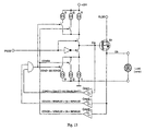
- FIG. 12 shows a triggering mechanism in a multiple-stage, current-controlled procedure
- FIG. 13 shows a switching arrangement for completing the procedure according to FIG. 12 ;
- FIG. 14 shows the relative power loss which depends on the output voltage.
- the present invention is based on further, active influencing of the switch edges in the switching facility in such a manner, that in the middle phase of the switching procedure in which power losses occur, a high increase is used, thus achieving a rapid bypass of this phase, while in the phases at the beginning and end of the switching procedure, in which hardly any power loss arises, the switch edge runs far more slowly.
- the phase of the increase is to be understood here as being in accordance with the amount of the gradient of the progression of the output voltage, and the progression when switching off should be shown with negative preliminary mathematical signs accordingly.
- FIG. 14 clearly shows this interrelationship.
- the switching resistance of the switching device is known to vary above the switching procedure. Depending on the switching resistance, a relative output voltage results, Ua/Ubat.
- FIG. 14 now shows the relative power loss Pv/Pvmax which has been added above this relative output voltage.
- the ideal switching speed is therefore proportionate to the effective power loss.
- a quadratic ideal characteristic curve results for the increase to be specified.
- the regulation according to this ideal characteristic curve is extremely complex, however, and is therefore preferably approximated in several stages.
- the broken curve approximates the optimum form over 3 stages, with the curve marked with stars approximating the optimum form over 5 stages.
- the increase, and therefore the switching speed, is thus controlled over the entire switching procedure with the corresponding approximation in accordance with the relative power loss which currently occurs.
- a triggering mechanism in at least three phases is suitable, whereby the increase in the middle phase is significantly higher than in the first and third phases, whereby the increase does not also need to be constant within the phases, but can also be adapted in stages or continuously.
- the sole decisive factor is that during the middle phase, the increase is significantly higher overall than in the first and third phases. Accordingly, reference is also made in the phases to a maximum increase.
- FIG. 6 A possible realisation of this switching procedure with a MOSFET switch is shown in FIG. 6 , whereby the gate is subjected to a different level of current in dependence on the voltage on the load element during switching, thus adapting the increase within the switching procedure. Therefore, in the middle phase of the switching procedure, which is critical in terms of power loss, the current and thus the increase is higher than during the beginning and end phases.
- controllable current sources and the corresponding control logic can provide a highly precise specification of the transitions, and if necessary, a very fine adaptation can be made.
- the supply voltage is here labelled as terminal 30 (KL 30 ) of the connection terminal commonly used for the supply on-board network.
- the supply voltage, UH, for the controllable current sources can here lie slightly above the potential on the terminal 30 , in order to be able to provide the gate-source voltage required for controlling purposes.
- a realisation with a bipolar power switch is also feasible, as shown in FIG. 7 .
- the control current is integrated with a capacitor, and this voltage is controlled with a buffer amplifier based on the bipolar transistor: here, the current is routed into the gate, and thus the speed of alteration of the switching transistor is routed in dependence on the condition of the output voltage Ua and/or the gate voltage Ug.
- the condition of the relevant signals, Ua and Ug, is here preferably recorded with comparators and the gate control currents are controlled via a logic to current converter.
- the realisation of the current triggering can either be achieved digitally via 2 or more switched current sources, or in analogue mode using current sources which can be modulated.
- FIG. 12 A practical exemplary embodiment and the related principle curves are subsequently shown in FIG. 12 .
- a phase with a slightly increased level of current is inserted (t 2 -t 3 , t 4 -t 5 ) during the switching procedure in the example given, in order to make the transitions “softer”.
- the transitions between the phases can be dampened to improve the rounding of the current progression with RC elements.
- the length, height and number of stages of the triggering currents, together with the precise position of the comparator thresholds, can be adapted to the corresponding requirements of the switching, and can ideally be parameterised.
- the procedure leads to a reduction in electromagnetic radiation in the radio frequency ranges of pulse-width modulate triggering mechanisms by systematically influencing the switching speed.
- the control of the speed of alteration of the switching state can be achieved in dependence on the condition of the output voltage Ua and/or the control voltage Ug, and the PWM control signal can activate the corresponding time control.
- the triggering current of the switch is controlled in dependence on the output voltage in such a manner that the effective switching speed forms an optimum between the switching power loss and the electromagnetic radiation.
- the control of the triggering current of the switch is therefore additionally achieved in dependence on the gate voltage in such a manner that the switching delay remains low.
- the voltage at the gate is quickly established with a high current, which does not yet affect the output of the switching device and thus also the HF interferences.
- a voltage on the control input Ug of the switching device is therefore monitored (COND 1 ).
- a current value above the first current value is fed in as long as the voltage on the control input is lower (t 0 -t 1 ) than a specified threshold voltage (VT), which approximately corresponds to the pinch-off voltage of the switching device in question.
- the current value is increased again (t 6 -t 7 ), when the voltage on the control input is lower than the difference between the supply voltage (Ubat) and the threshold voltage (VT).
- the control of the triggering current can either be achieved digitally using switched current sources, or in analogue mode using current sources which can be modulated.
- the switching arrangement is designed to adapt the switching speed to different configurations (wire length, cabling, current, switching frequency, etc.) in such a manner that it can be parameterised.
- the invention is directly integrated into an intelligent power switch.
- the space and cost savings are particularly high.
- the procedure and the switching arrangement are particularly suitable for triggering lamps as essentially ohmic loads, in particular for motor vehicles.
Landscapes
- Electronic Switches (AREA)
- Inverter Devices (AREA)
- Dc-Dc Converters (AREA)
Applications Claiming Priority (4)
| Application Number | Priority Date | Filing Date | Title |
|---|---|---|---|
| DE10358276 | 2003-12-11 | ||
| DE10358276A DE10358276A1 (de) | 2003-12-11 | 2003-12-11 | Verfahren und Schaltungsanordnung zur Ansteuerung eines Lastelements mittels eines elektronischen Schaltelements im Laststromkreis |
| DE10358276.2 | 2003-12-11 | ||
| PCT/DE2004/002715 WO2005057788A2 (fr) | 2003-12-11 | 2004-12-10 | Procede et dispositif de commutation pour commander un element de charge au moyen d'un element de commutation electronique dans le circuit electrique de charge |
Publications (2)
| Publication Number | Publication Date |
|---|---|
| US20070103133A1 US20070103133A1 (en) | 2007-05-10 |
| US8035363B2 true US8035363B2 (en) | 2011-10-11 |
Family
ID=34672670
Family Applications (1)
| Application Number | Title | Priority Date | Filing Date |
|---|---|---|---|
| US10/582,462 Expired - Fee Related US8035363B2 (en) | 2003-12-11 | 2004-12-10 | Procedure and a switching arrangement for triggering a load element using an electronic switching element in a load circuit |
Country Status (4)
| Country | Link |
|---|---|
| US (1) | US8035363B2 (fr) |
| EP (1) | EP1692766B1 (fr) |
| DE (3) | DE10358276A1 (fr) |
| WO (1) | WO2005057788A2 (fr) |
Cited By (2)
| Publication number | Priority date | Publication date | Assignee | Title |
|---|---|---|---|---|
| WO2013130480A1 (fr) * | 2012-03-01 | 2013-09-06 | Sandisk Technologies Inc. | Interrupteur à vitesse de balayage programmable |
| US20130241604A1 (en) * | 2012-03-14 | 2013-09-19 | Samsung Electronics Co., Ltd. | Power module including leakage current protection circuit |
Families Citing this family (10)
| Publication number | Priority date | Publication date | Assignee | Title |
|---|---|---|---|---|
| TW200820609A (en) * | 2006-03-31 | 2008-05-01 | Nxp Bv | Method and system for signal control |
| DE102007040783A1 (de) | 2007-08-28 | 2009-03-12 | Conti Temic Microelectronic Gmbh | Verfahren zur Ansteuerung von nichtlinearen Lastelementen |
| EP2296136A1 (fr) * | 2009-09-07 | 2011-03-16 | Nxp B.V. | Circuit de contrôle d'unité de rétro-éclairage |
| EP2437134B1 (fr) | 2010-10-01 | 2013-07-31 | STMicroelectronics (Rousset) SAS | Contrôleur à faibles émissions électromagnétiques |
| DE102012104590A1 (de) * | 2012-05-29 | 2013-12-05 | Infineon Technologies Ag | Treiberschaltung |
| US20140103897A1 (en) * | 2012-10-17 | 2014-04-17 | Qualcomm Incorporated | Glitch suppression in dc-to-dc power conversion |
| DE102013220842B4 (de) * | 2013-10-15 | 2021-06-17 | Vitesco Technologies GmbH | Verfahren zum Schalten eines Zyklus in einer Leistungstransistorschaltung |
| US9312848B2 (en) * | 2014-06-30 | 2016-04-12 | Qualcomm, Incorporated | Glitch suppression in an amplifier |
| EP3057231B1 (fr) * | 2015-02-16 | 2019-04-10 | Power Integrations Switzerland GmbH | Circuit de commande et procédé de commande destiné à commuter un interrupteur semi-conducteur de puissance |
| JP6889047B2 (ja) * | 2017-06-30 | 2021-06-18 | ローム株式会社 | スイッチング制御回路 |
Citations (13)
| Publication number | Priority date | Publication date | Assignee | Title |
|---|---|---|---|---|
| EP0340731A2 (fr) | 1988-05-02 | 1989-11-08 | Kabushiki Kaisha Toshiba | Circuit de sortie pour circuit intégré semi-conducteur avec bruit de ligne d'alimentation réduit |
| DE4229342A1 (de) | 1992-09-04 | 1994-03-10 | Thomson Brandt Gmbh | Verfahren und Vorrichtung zur Ansteuerung mit gepulsten Signalen |
| DE4330996A1 (de) | 1993-09-13 | 1995-03-16 | Bosch Gmbh Robert | Steuereinrichtung für einen elektrischen, insbesondere einen induktiven Verbraucher |
| DE4413546A1 (de) | 1994-04-19 | 1995-10-26 | Walter Marks | Gleichstrom-Steuerschaltung |
| US5479086A (en) * | 1990-04-30 | 1995-12-26 | Fraunhofer Gesellschaft Zur Forderung Der Angewandten Forschung E.V. | Process and device for reducing the inrush current when powering aninductive load |
| DE19619399A1 (de) | 1996-05-14 | 1997-11-20 | Telefunken Microelectron | Schaltvorrichtung mit einem Leistungs-FET und einer induktiven Last |
| DE19848829A1 (de) | 1998-10-22 | 2000-05-04 | Siemens Ag | Anordnung zur Formung von Schaltflanken in einem Leitungsstromkreis |
| US6094086A (en) | 1997-05-12 | 2000-07-25 | Industrial Technology Research Institute | High drive CMOS output buffer with fast and slow speed controls |
| DE19945432A1 (de) | 1999-09-22 | 2001-04-12 | Infineon Technologies Ag | Schaltungsanordnung zum Ansteuern einer Last mit reduzierter Störabstrahlung |
| US20010040470A1 (en) | 1998-12-02 | 2001-11-15 | Cyrille Brando | Method and device for driving a power output stage |
| DE10061563A1 (de) | 2000-12-06 | 2002-06-27 | Rubitec Gesellschaft Fuer Innovation & Technologie Ruhr Univ Bochum Mbh | Verfahren und Vorrichtung zum Ein- und Ausschalten von Leistungshalbleitern, insbesondere für ein drehzahlvariables Betreiben einer Asynchronmaschine, ein Betreiben einer Zündschaltung für Ottomotoren, sowie Schaltnetzteil |
| DE10143432C1 (de) | 2001-09-05 | 2003-02-27 | Daimler Chrysler Ag | Treiberschaltung und Ansteuerverfahren für einen feldgesteuerten Leistungsschalter |
| US6784721B2 (en) * | 2001-01-17 | 2004-08-31 | Stmicroelectronics S.R.L. | Driver circuit for soft turning on a power element connected to an inductive load |
Family Cites Families (1)
| Publication number | Priority date | Publication date | Assignee | Title |
|---|---|---|---|---|
| DE19841719C2 (de) * | 1998-09-11 | 2002-04-25 | St Microelectronics Gmbh | Schaltungsanordnung zur Flankensteilheitsformung |
-
2003
- 2003-12-11 DE DE10358276A patent/DE10358276A1/de not_active Withdrawn
-
2004
- 2004-12-10 DE DE112004002738T patent/DE112004002738D2/de not_active Expired - Fee Related
- 2004-12-10 WO PCT/DE2004/002715 patent/WO2005057788A2/fr active IP Right Grant
- 2004-12-10 EP EP04802920A patent/EP1692766B1/fr active Active
- 2004-12-10 US US10/582,462 patent/US8035363B2/en not_active Expired - Fee Related
- 2004-12-10 DE DE502004007579T patent/DE502004007579D1/de active Active
Patent Citations (14)
| Publication number | Priority date | Publication date | Assignee | Title |
|---|---|---|---|---|
| EP0340731A2 (fr) | 1988-05-02 | 1989-11-08 | Kabushiki Kaisha Toshiba | Circuit de sortie pour circuit intégré semi-conducteur avec bruit de ligne d'alimentation réduit |
| US5479086A (en) * | 1990-04-30 | 1995-12-26 | Fraunhofer Gesellschaft Zur Forderung Der Angewandten Forschung E.V. | Process and device for reducing the inrush current when powering aninductive load |
| DE4229342A1 (de) | 1992-09-04 | 1994-03-10 | Thomson Brandt Gmbh | Verfahren und Vorrichtung zur Ansteuerung mit gepulsten Signalen |
| DE4330996A1 (de) | 1993-09-13 | 1995-03-16 | Bosch Gmbh Robert | Steuereinrichtung für einen elektrischen, insbesondere einen induktiven Verbraucher |
| DE4413546A1 (de) | 1994-04-19 | 1995-10-26 | Walter Marks | Gleichstrom-Steuerschaltung |
| DE19619399A1 (de) | 1996-05-14 | 1997-11-20 | Telefunken Microelectron | Schaltvorrichtung mit einem Leistungs-FET und einer induktiven Last |
| US6094086A (en) | 1997-05-12 | 2000-07-25 | Industrial Technology Research Institute | High drive CMOS output buffer with fast and slow speed controls |
| DE19848829A1 (de) | 1998-10-22 | 2000-05-04 | Siemens Ag | Anordnung zur Formung von Schaltflanken in einem Leitungsstromkreis |
| US20010040470A1 (en) | 1998-12-02 | 2001-11-15 | Cyrille Brando | Method and device for driving a power output stage |
| DE19945432A1 (de) | 1999-09-22 | 2001-04-12 | Infineon Technologies Ag | Schaltungsanordnung zum Ansteuern einer Last mit reduzierter Störabstrahlung |
| US6747505B1 (en) * | 1999-09-22 | 2004-06-08 | Infineon Technologies Ag | Circuit configuration for controlling a load with reduced noise emission |
| DE10061563A1 (de) | 2000-12-06 | 2002-06-27 | Rubitec Gesellschaft Fuer Innovation & Technologie Ruhr Univ Bochum Mbh | Verfahren und Vorrichtung zum Ein- und Ausschalten von Leistungshalbleitern, insbesondere für ein drehzahlvariables Betreiben einer Asynchronmaschine, ein Betreiben einer Zündschaltung für Ottomotoren, sowie Schaltnetzteil |
| US6784721B2 (en) * | 2001-01-17 | 2004-08-31 | Stmicroelectronics S.R.L. | Driver circuit for soft turning on a power element connected to an inductive load |
| DE10143432C1 (de) | 2001-09-05 | 2003-02-27 | Daimler Chrysler Ag | Treiberschaltung und Ansteuerverfahren für einen feldgesteuerten Leistungsschalter |
Cited By (4)
| Publication number | Priority date | Publication date | Assignee | Title |
|---|---|---|---|---|
| WO2013130480A1 (fr) * | 2012-03-01 | 2013-09-06 | Sandisk Technologies Inc. | Interrupteur à vitesse de balayage programmable |
| US8922176B2 (en) | 2012-03-01 | 2014-12-30 | Sandisk Technologies Inc. | Programmable slew rate power switch |
| US20130241604A1 (en) * | 2012-03-14 | 2013-09-19 | Samsung Electronics Co., Ltd. | Power module including leakage current protection circuit |
| US9088151B2 (en) * | 2012-03-14 | 2015-07-21 | Samsung Electronics Co., Ltd. | Power module including leakage current protection circuit |
Also Published As
| Publication number | Publication date |
|---|---|
| WO2005057788A2 (fr) | 2005-06-23 |
| EP1692766A2 (fr) | 2006-08-23 |
| DE10358276A1 (de) | 2005-07-21 |
| DE112004002738D2 (de) | 2006-11-23 |
| EP1692766B1 (fr) | 2008-07-09 |
| US20070103133A1 (en) | 2007-05-10 |
| WO2005057788A3 (fr) | 2005-07-28 |
| DE502004007579D1 (de) | 2008-08-21 |
Similar Documents
| Publication | Publication Date | Title |
|---|---|---|
| US8035363B2 (en) | Procedure and a switching arrangement for triggering a load element using an electronic switching element in a load circuit | |
| US6891342B2 (en) | Drive apparatus for PWM control of two inductive loads with reduced generation of electrical noise | |
| US4504779A (en) | Electrical load drive and control system | |
| US5929692A (en) | Ripple cancellation circuit with fast load response for switch mode voltage regulators with synchronous rectification | |
| US7405609B2 (en) | Circuit arrangement for driving an electrical circuit breaker at high voltage potential | |
| JP3332265B2 (ja) | ターンオフスルーレートを制御する高電位側ドライバ回路及び方法 | |
| US7253540B1 (en) | Method for operating a parallel arrangement of semiconductor power switches | |
| US20240022946A1 (en) | Slew rate controllable system for powering electric machine | |
| US10389246B1 (en) | Resonant rectified discontinuous switching regulator with inductor preflux | |
| US10186945B1 (en) | Resonant switching regulator with continuous current | |
| AU731189B1 (en) | A switch input circuit | |
| US9083333B2 (en) | Switching circuit | |
| US8294443B2 (en) | Overshoot/undershoot elimination for a PWM converter which requires voltage slewing | |
| US5801458A (en) | Direct current control circuit | |
| CN112202317A (zh) | 栅极驱动装置及功率转换装置 | |
| US20050207194A1 (en) | Control device and process of a converter and converter and electrical installation comprising such a device | |
| CN113037063B (zh) | 过零自校准电路、dc/dc转换器及电源管理芯片 | |
| US11843368B2 (en) | Method for reducing oscillation during turn on of a power transistor by regulating the gate switching speed control of its complementary power transistor | |
| US20010035743A1 (en) | Circuit configuration for controlling a switching device for switching an electrical consumer and method for limiting a time deviation of a switching current of a consumer | |
| JP4135403B2 (ja) | スイッチング回路及び電源回路 | |
| US10778213B2 (en) | Driving circuit for output transistor | |
| CN110945766B (zh) | 用于操控脉冲宽度调制变流器的方法、控制设备、变流装置和电驱动系统 | |
| JP4175805B2 (ja) | 電流を調整するプログラマブルロジックコントローラ(plc)、その回路及びその方法 | |
| DE10143432C1 (de) | Treiberschaltung und Ansteuerverfahren für einen feldgesteuerten Leistungsschalter | |
| US5798914A (en) | Power factor of a rectified power supply |
Legal Events
| Date | Code | Title | Description |
|---|---|---|---|
| AS | Assignment |
Owner name: CONTI TEMIC MICROELECTRONIC, GMBH, GERMANY Free format text: ASSIGNMENT OF ASSIGNORS INTEREST;ASSIGNORS:JOOS, ULI;LENK, ARMIN;REEL/FRAME:017999/0138 Effective date: 20060308 Owner name: CONTI TERMIC MICROELECTRONIC, GMBH, GERMANY Free format text: ASSIGNMENT OF ASSIGNORS INTEREST;ASSIGNORS:JOOS, ULI;LENK, ARMIN;REEL/FRAME:017999/0138 Effective date: 20060308 |
|
| ZAAA | Notice of allowance and fees due |
Free format text: ORIGINAL CODE: NOA |
|
| ZAAB | Notice of allowance mailed |
Free format text: ORIGINAL CODE: MN/=. |
|
| STCF | Information on status: patent grant |
Free format text: PATENTED CASE |
|
| FEPP | Fee payment procedure |
Free format text: PAYOR NUMBER ASSIGNED (ORIGINAL EVENT CODE: ASPN); ENTITY STATUS OF PATENT OWNER: LARGE ENTITY |
|
| FPAY | Fee payment |
Year of fee payment: 4 |
|
| MAFP | Maintenance fee payment |
Free format text: PAYMENT OF MAINTENANCE FEE, 8TH YEAR, LARGE ENTITY (ORIGINAL EVENT CODE: M1552); ENTITY STATUS OF PATENT OWNER: LARGE ENTITY Year of fee payment: 8 |
|
| FEPP | Fee payment procedure |
Free format text: MAINTENANCE FEE REMINDER MAILED (ORIGINAL EVENT CODE: REM.); ENTITY STATUS OF PATENT OWNER: LARGE ENTITY |
|
| LAPS | Lapse for failure to pay maintenance fees |
Free format text: PATENT EXPIRED FOR FAILURE TO PAY MAINTENANCE FEES (ORIGINAL EVENT CODE: EXP.); ENTITY STATUS OF PATENT OWNER: LARGE ENTITY |
|
| STCH | Information on status: patent discontinuation |
Free format text: PATENT EXPIRED DUE TO NONPAYMENT OF MAINTENANCE FEES UNDER 37 CFR 1.362 |
|
| FP | Lapsed due to failure to pay maintenance fee |
Effective date: 20231011 |