US8035096B2 - Switching device, rewritable logic integrated circuit, and memory device - Google Patents
Switching device, rewritable logic integrated circuit, and memory device Download PDFInfo
- Publication number
- US8035096B2 US8035096B2 US12/278,611 US27861107A US8035096B2 US 8035096 B2 US8035096 B2 US 8035096B2 US 27861107 A US27861107 A US 27861107A US 8035096 B2 US8035096 B2 US 8035096B2
- Authority
- US
- United States
- Prior art keywords
- electrode
- switching device
- conductive layer
- ion conductive
- voltage
- Prior art date
- Legal status (The legal status is an assumption and is not a legal conclusion. Google has not performed a legal analysis and makes no representation as to the accuracy of the status listed.)
- Active, expires
Links
Images


Classifications
-
- H—ELECTRICITY
- H03—ELECTRONIC CIRCUITRY
- H03K—PULSE TECHNIQUE
- H03K19/00—Logic circuits, i.e. having at least two inputs acting on one output; Inverting circuits
- H03K19/02—Logic circuits, i.e. having at least two inputs acting on one output; Inverting circuits using specified components
- H03K19/173—Logic circuits, i.e. having at least two inputs acting on one output; Inverting circuits using specified components using elementary logic circuits as components
-
- G—PHYSICS
- G11—INFORMATION STORAGE
- G11C—STATIC STORES
- G11C13/00—Digital stores characterised by the use of storage elements not covered by groups G11C11/00, G11C23/00, or G11C25/00
- G11C13/0002—Digital stores characterised by the use of storage elements not covered by groups G11C11/00, G11C23/00, or G11C25/00 using resistive RAM [RRAM] elements
- G11C13/0007—Digital stores characterised by the use of storage elements not covered by groups G11C11/00, G11C23/00, or G11C25/00 using resistive RAM [RRAM] elements comprising metal oxide memory material, e.g. perovskites
-
- G—PHYSICS
- G11—INFORMATION STORAGE
- G11C—STATIC STORES
- G11C13/00—Digital stores characterised by the use of storage elements not covered by groups G11C11/00, G11C23/00, or G11C25/00
- G11C13/0002—Digital stores characterised by the use of storage elements not covered by groups G11C11/00, G11C23/00, or G11C25/00 using resistive RAM [RRAM] elements
- G11C13/0009—RRAM elements whose operation depends upon chemical change
- G11C13/0011—RRAM elements whose operation depends upon chemical change comprising conductive bridging RAM [CBRAM] or programming metallization cells [PMCs]
-
- G—PHYSICS
- G11—INFORMATION STORAGE
- G11C—STATIC STORES
- G11C13/00—Digital stores characterised by the use of storage elements not covered by groups G11C11/00, G11C23/00, or G11C25/00
- G11C13/0002—Digital stores characterised by the use of storage elements not covered by groups G11C11/00, G11C23/00, or G11C25/00 using resistive RAM [RRAM] elements
- G11C13/0021—Auxiliary circuits
- G11C13/0069—Writing or programming circuits or methods
-
- G—PHYSICS
- G11—INFORMATION STORAGE
- G11C—STATIC STORES
- G11C13/00—Digital stores characterised by the use of storage elements not covered by groups G11C11/00, G11C23/00, or G11C25/00
- G11C13/02—Digital stores characterised by the use of storage elements not covered by groups G11C11/00, G11C23/00, or G11C25/00 using elements whose operation depends upon chemical change
-
- H—ELECTRICITY
- H03—ELECTRONIC CIRCUITRY
- H03K—PULSE TECHNIQUE
- H03K17/00—Electronic switching or gating, i.e. not by contact-making and –breaking
- H03K17/08—Modifications for protecting switching circuit against overcurrent or overvoltage
- H03K17/081—Modifications for protecting switching circuit against overcurrent or overvoltage without feedback from the output circuit to the control circuit
- H03K17/0812—Modifications for protecting switching circuit against overcurrent or overvoltage without feedback from the output circuit to the control circuit by measures taken in the control circuit
-
- H—ELECTRICITY
- H03—ELECTRONIC CIRCUITRY
- H03K—PULSE TECHNIQUE
- H03K17/00—Electronic switching or gating, i.e. not by contact-making and –breaking
- H03K17/51—Electronic switching or gating, i.e. not by contact-making and –breaking characterised by the components used
- H03K17/56—Electronic switching or gating, i.e. not by contact-making and –breaking characterised by the components used by the use, as active elements, of semiconductor devices
-
- H—ELECTRICITY
- H03—ELECTRONIC CIRCUITRY
- H03K—PULSE TECHNIQUE
- H03K19/00—Logic circuits, i.e. having at least two inputs acting on one output; Inverting circuits
- H03K19/02—Logic circuits, i.e. having at least two inputs acting on one output; Inverting circuits using specified components
- H03K19/08—Logic circuits, i.e. having at least two inputs acting on one output; Inverting circuits using specified components using semiconductor devices
-
- H—ELECTRICITY
- H10—SEMICONDUCTOR DEVICES; ELECTRIC SOLID-STATE DEVICES NOT OTHERWISE PROVIDED FOR
- H10N—ELECTRIC SOLID-STATE DEVICES NOT OTHERWISE PROVIDED FOR
- H10N70/00—Solid-state devices having no potential barriers, and specially adapted for rectifying, amplifying, oscillating or switching
- H10N70/011—Manufacture or treatment of multistable switching devices
- H10N70/021—Formation of switching materials, e.g. deposition of layers
- H10N70/026—Formation of switching materials, e.g. deposition of layers by physical vapor deposition, e.g. sputtering
-
- H—ELECTRICITY
- H10—SEMICONDUCTOR DEVICES; ELECTRIC SOLID-STATE DEVICES NOT OTHERWISE PROVIDED FOR
- H10N—ELECTRIC SOLID-STATE DEVICES NOT OTHERWISE PROVIDED FOR
- H10N70/00—Solid-state devices having no potential barriers, and specially adapted for rectifying, amplifying, oscillating or switching
- H10N70/011—Manufacture or treatment of multistable switching devices
- H10N70/061—Shaping switching materials
-
- H—ELECTRICITY
- H10—SEMICONDUCTOR DEVICES; ELECTRIC SOLID-STATE DEVICES NOT OTHERWISE PROVIDED FOR
- H10N—ELECTRIC SOLID-STATE DEVICES NOT OTHERWISE PROVIDED FOR
- H10N70/00—Solid-state devices having no potential barriers, and specially adapted for rectifying, amplifying, oscillating or switching
- H10N70/20—Multistable switching devices, e.g. memristors
- H10N70/24—Multistable switching devices, e.g. memristors based on migration or redistribution of ionic species, e.g. anions, vacancies
- H10N70/245—Multistable switching devices, e.g. memristors based on migration or redistribution of ionic species, e.g. anions, vacancies the species being metal cations, e.g. programmable metallization cells
-
- H—ELECTRICITY
- H10—SEMICONDUCTOR DEVICES; ELECTRIC SOLID-STATE DEVICES NOT OTHERWISE PROVIDED FOR
- H10N—ELECTRIC SOLID-STATE DEVICES NOT OTHERWISE PROVIDED FOR
- H10N70/00—Solid-state devices having no potential barriers, and specially adapted for rectifying, amplifying, oscillating or switching
- H10N70/801—Constructional details of multistable switching devices
- H10N70/821—Device geometry
- H10N70/826—Device geometry adapted for essentially vertical current flow, e.g. sandwich or pillar type devices
-
- H—ELECTRICITY
- H10—SEMICONDUCTOR DEVICES; ELECTRIC SOLID-STATE DEVICES NOT OTHERWISE PROVIDED FOR
- H10N—ELECTRIC SOLID-STATE DEVICES NOT OTHERWISE PROVIDED FOR
- H10N70/00—Solid-state devices having no potential barriers, and specially adapted for rectifying, amplifying, oscillating or switching
- H10N70/801—Constructional details of multistable switching devices
- H10N70/841—Electrodes
- H10N70/8416—Electrodes adapted for supplying ionic species
-
- H—ELECTRICITY
- H10—SEMICONDUCTOR DEVICES; ELECTRIC SOLID-STATE DEVICES NOT OTHERWISE PROVIDED FOR
- H10N—ELECTRIC SOLID-STATE DEVICES NOT OTHERWISE PROVIDED FOR
- H10N70/00—Solid-state devices having no potential barriers, and specially adapted for rectifying, amplifying, oscillating or switching
- H10N70/801—Constructional details of multistable switching devices
- H10N70/881—Switching materials
- H10N70/883—Oxides or nitrides
- H10N70/8833—Binary metal oxides, e.g. TaOx
-
- G—PHYSICS
- G11—INFORMATION STORAGE
- G11C—STATIC STORES
- G11C13/00—Digital stores characterised by the use of storage elements not covered by groups G11C11/00, G11C23/00, or G11C25/00
- G11C13/0002—Digital stores characterised by the use of storage elements not covered by groups G11C11/00, G11C23/00, or G11C25/00 using resistive RAM [RRAM] elements
- G11C13/0021—Auxiliary circuits
- G11C13/0069—Writing or programming circuits or methods
- G11C2013/0071—Write using write potential applied to access device gate
-
- G—PHYSICS
- G11—INFORMATION STORAGE
- G11C—STATIC STORES
- G11C2213/00—Indexing scheme relating to G11C13/00 for features not covered by this group
- G11C2213/10—Resistive cells; Technology aspects
- G11C2213/11—Metal ion trapping, i.e. using memory material including cavities, pores or spaces in form of tunnels or channels wherein metal ions can be trapped but do not react and form an electro-deposit creating filaments or dendrites
-
- G—PHYSICS
- G11—INFORMATION STORAGE
- G11C—STATIC STORES
- G11C2213/00—Indexing scheme relating to G11C13/00 for features not covered by this group
- G11C2213/10—Resistive cells; Technology aspects
- G11C2213/15—Current-voltage curve
-
- G—PHYSICS
- G11—INFORMATION STORAGE
- G11C—STATIC STORES
- G11C2213/00—Indexing scheme relating to G11C13/00 for features not covered by this group
- G11C2213/30—Resistive cell, memory material aspects
- G11C2213/32—Material having simple binary metal oxide structure
-
- G—PHYSICS
- G11—INFORMATION STORAGE
- G11C—STATIC STORES
- G11C2213/00—Indexing scheme relating to G11C13/00 for features not covered by this group
- G11C2213/30—Resistive cell, memory material aspects
- G11C2213/34—Material includes an oxide or a nitride
-
- G—PHYSICS
- G11—INFORMATION STORAGE
- G11C—STATIC STORES
- G11C2213/00—Indexing scheme relating to G11C13/00 for features not covered by this group
- G11C2213/50—Resistive cell structure aspects
- G11C2213/52—Structure characterized by the electrode material, shape, etc.
-
- G—PHYSICS
- G11—INFORMATION STORAGE
- G11C—STATIC STORES
- G11C2213/00—Indexing scheme relating to G11C13/00 for features not covered by this group
- G11C2213/70—Resistive array aspects
- G11C2213/79—Array wherein the access device being a transistor
-
- H—ELECTRICITY
- H10—SEMICONDUCTOR DEVICES; ELECTRIC SOLID-STATE DEVICES NOT OTHERWISE PROVIDED FOR
- H10B—ELECTRONIC MEMORY DEVICES
- H10B63/00—Resistance change memory devices, e.g. resistive RAM [ReRAM] devices
- H10B63/30—Resistance change memory devices, e.g. resistive RAM [ReRAM] devices comprising selection components having three or more electrodes, e.g. transistors
Definitions
- the present invention relates to a switching device utilizing electrochemical reaction, a rewritable logic integrated circuit having the switching device, and a memory device.
- a large number of integrated circuits are currently used in electronic apparatuses. Most of the integrated circuits that are used in the electronic apparatuses are application specific integrated circuits (ASICs).
- ASICs application specific integrated circuits
- the application specific integrated circuit is a dedicated circuit designed for a specific electronic apparatus.
- programmable logic ICs rewritable logic integrated circuits
- FPGA Field-Programmable Gate Array
- DRP Dynamic Reconfigurable Processor
- a switching device which utilizes metal ion migration and electrochemical reaction in an ion conductor (a solid through which ions can migrate freely) (see, for example, WO 2003/094227).
- the switching device disclosed in WO 2003/094227 has a smaller size and a lower ON-resistance than semiconductor switches (MOSFETs) often used in the conventional programmable logic ICs.
- FIG. 7 is a schematic sectional view showing the configuration of the switching device disclosed in WO 2003/094227.
- the switching device has first electrode 11 , and second electrode 12 laminated on first electrode 11 via ion conductive layer 13 (referred to as a “solid electrolyte” in Patent Document 1).
- ion conductive layer 13 serves as a medium through which metal ions are conducted.
- Second electrode 12 is grounded, and a negative voltage is applied to first electrode 11 .
- metal in second electrode 12 is dissolved into ion conductive layer 13 as metal ions.
- the metal ions in ion conductive layer 13 are precipitated on a surface of first electrode 11 as metal.
- the precipitated metal forms metal dendrite connecting first electrode 11 and second electrode 12 .
- the metal dendrite is a metal precipitate resulting from precipitation of the metal ions contained in ion conductive layer 13 .
- the metal dendrite electrically connects first electrode 11 and second electrode 12 together to turn on the switch.
- first electrode 11 is grounded, a positive voltage is applied to first electrode 11 . Then, the metal dendrite is dissolved into ion conductive layer 13 , and a part of the metal dendrite is severed. This electrically disconnects first electrode 11 from second electrode 12 to turn off the switch. Electrical characteristics change before the electric connection is completely cut. For example, the electric resistance between first electrode 11 and second electrode 12 increases or inter-electrode capacitance changes before the electric connection is finally cut. Furthermore, a desirable material for first electrode 11 is a material which does not feed metal ions into the ion conductive layer when the voltage is applied to first electrode 11 . Additionally, the negative voltage may be applied to first electrode 11 again in order to change the off state to the on state.
- JOURNAL OF SOLID STATE CIRCUITS, Vol. 40, No. 1, 2005, pp. 168 to 176 proposes that such a switching device as shown in FIG. 7 be used as a wiring switch for the programmable device.
- this switching device reduces the switch area to 1/30 and the switch resistance to 1/50.
- the switching device can be formed into a wiring layer. This is expected to reduce the chip area and to improve possible wiring delays.
- the size of the logic cells in the programmable logic IC can be reduced, allowing a drastic increase in circuit utilization efficiency. As a result, the chip area is reduced to 1/10, and power efficiency is tripled.
- the large chip size and low power efficiency of the conventional programmable logic IC limits the range of applications thereof.
- programmable logic ICs using such a switching device as shown in FIG. 7 can cover a wider application range.
- WO 2003/094227 discloses Cu/Cu 2 S, Ag/Ag 2 S, and the like as examples of a combination of an electrode material and an ion conductive layer. Any of the material combinations involves the application of a voltage (switching voltage) of about 0.05 to 0.30 [V] to first electrode 11 ( FIG. 7 ) in order to change the switching device from the on state to the off state or from the off state to the on state.
- a voltage indicating one of two types of information that is, an operating voltage for the logic IC
- a voltage indicating the other type of information is 0.0 [V].
- a Vdd [V] that is currently often used in silicon integrated circuits is about 1.0 to 2.0 [V].
- the switching device disclosed in WO 2003/094227 has a switching voltage of at most 0.30 [V]. Consequently, if the Vdd of the logic signal is 1.0 [V], the switching voltage is lower than Vdd. Thus, every time a logic signal with the voltage Vdd [V] is input to the switching device, a voltage of 1.0 [V] is applied to the first electrode. The logic signal may thus change the state of the switch. In this case, a fatal problem may occur; the switch may not function. Therefore, a higher switching voltage needs to be set to stabilize the switching device.
- a time equal to or longer than the product life (generally 10 years) of the programmable logic IC is required to hold the state of the switching device (the time required to maintain non-volatility).
- Heat energy at room temperature is generally 26.0 [meV].
- the switching voltage is closer to 26.0 [mV]
- thermal noise may be generated and is likely to cause the switching state to change voluntarily. Therefore, the switching voltage also needs to be increased in order to allow the state of the switching device to be maintained for a longer time.
- An object of the present invention is to solve the problems of the related art. Specifically, an object of the present invention is to provide a switching device for which a switching voltage is set higher than that for the related art, a rewritable logic integrated circuit using the switching device, and a memory device.
- a switching device includes a first electrode and a second electrode laminated via at least one ion conductive layer.
- Metal ions are fed from the second electrode to the ion conductive layer and precipitated in the ion conductive layer as metal to electrically connect the first and second electrodes together.
- the precipitated metal is dissolved into the ion conductive layer to electrically disconnect the first and second electrodes from each other.
- metal ions are fed from an ion supply layer provided between the second electrode and the ion conductive layer, to the ion conductive layer and precipitated in the ion conductive layer as metal to electrically connect the first and second electrodes together.
- the precipitated metal is dissolved into the ion conductive layer to electrically disconnect the first and second electrodes from each other.
- the ion conductive layer contains titanium oxide.
- the titanium oxide contained in the ion conductive layer desirably has a stoichiometric composition of oxide and titanium in which the ratio of oxide to titanium is 2:1.
- a material for the second electrode is copper, and a material for the first electrode avoids supplying metal ions to the ion conductive layer.
- the switching device further includes a circuit that limits current flowing between the first and second electrodes when a voltage is applied to between the first and second electrodes.
- a rewritable logic integrated circuit can be configured by using the switching device according to the present invention as a switch that switches on and off a connection between logic cells.
- a memory device can be configured by using the switching device according to the present invention and a transistor device that detects whether the switching device is in an on state or an off state.
- the first electrode of the switching device is connected to a drain of the transistor device.
- the second electrode of the switching device is connected to a first bit line.
- a source of the transistor device is connected to a second bit line different from the first bit line.
- a gate of the transistor device is connected to a word line.
- FIG. 1 is a schematic sectional view showing an example of an exemplary embodiment of a switching device according to the present invention
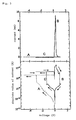
- FIG. 2 is a diagram showing leakage current characteristics of titanium oxide
- FIG. 3 is a diagram showing switching characteristics of the switching device according to the present invention.
- FIG. 4 is a diagram showing an example of the configuration of a current control circuit in the switching device according to the present invention.
- FIG. 5 is a schematic diagram showing an example of the configuration of a programmable logic IC using the switching device according to the present invention
- FIG. 6 is a schematic circuit diagram showing an example of the configuration of a memory device using the switching device according to the present invention.
- FIG. 7 is a schematic sectional view showing an example of the configuration of a conventional switching device.
- FIG. 1 is a schematic sectional view showing the basic structure of the switching device in the present example.
- the switching device in the present example has silicon substrate 25 having a surface covered with silicon oxide film 26 .
- First electrode 21 , ion conductive layer 23 , and second electrode 22 are laminated on silicon oxide film 26 .
- first electrode 21 and second electrode 22 are laminated across ion conductive layer 23 .
- only one ion conductive layer 23 is illustrated.
- at least two ion conductive layers 23 may be laminated, with first electrode 21 and second electrode 22 provided outside laminated ion conductive layer 23 .
- Ion conductive layer 23 is formed of a titanium oxide film having a 15.0 [nm] thickness.
- First electrode 21 is formed of a platinum film having a 100.0 [nm] thickness.
- Second electrode 22 is formed of a copper film having a 100.0 [nm] thickness.
- first electrode 21 is covered with a silicon oxide film (insulating layer 24 ) in which opening 27 is formed, and a part of first electrode 21 is in contact with ion conductive layer 23 in opening 27 in insulating layer 24 . That is, the switching device in the present example, a switch portion in which the metal is actually precipitated is formed in opening 27 in insulating layer 24 .
- the junction area between first electrode 21 and ion conductive layer 23 depends on the bottom surface area of opening 27 .
- the junction area is determined by the bottom area of opening 27 even though the pattern of first electrode 21 , second electrode 22 , and ion conductive layer 23 is larger than the pattern of opening 27 . Consequently, when a plurality of switching devices are formed in a substrate, the switching characteristics of the devices can be made uniform by accurately forming opening 27 in each of the devices. Thus, the pattern of second electrode 22 , first electrode 21 , and ion conductive layer 23 need not be formed as accurately as the pattern of opening 27 . Furthermore, as shown in FIG. 1 , second electrode 22 and first electrode 21 are separated from each other by insulating layer 24 except for the switch portion. Thus, possible leakage current from the switching device can be inhibited while the switching device is off.
- the inventors attempted to set an applied voltage required to change the switching device from the off state to the on state, that is, the switching voltage, to any value by controlling the migration speed of the metal ions, the precipitation speed of the metal, and the dissolution speed of the metal.
- Table 1 shows a diffusion coefficient and the switching voltage for combinations of materials for the ion conductive layer and the metal ions.
- the combinations are classified by alphabets A to H.
- the diffusion coefficient is proportional to the ion conductivity, and the ion conductivity increases consistently with the diffusion coefficient.
- the switching voltages for the combinations other than those D and E were measured using switching devices configured as shown in FIG. 8 and produced by the inventors.
- the switching voltage is about 0.2 [V], which is much lower than the logic voltage, 1.0 [V].
- Each of the combinations A to E uses a material composed of a combination of a chalcogen element (S, Se, Ge, or Te) and a metal element (Ag or Cu) as the ion conductive layer.
- a chalcogen element S, Se, Ge, or Te
- a metal element Ag or Cu
- Each of these compounds is a halide that is a kind of chalcogenide.
- Many silver halides and copper halides Cu 2 S, Ag 2 S, AgI, and the like
- a high ion conductivity that is significantly characteristic of materials such as super ion conductors is due to a structural defect based on the crystal structure of these compounds. In these compounds, a large number of vacant lattices corresponding to missing metal or chalcogen elements are present in the crystal and form a site through which metal ions are conducted.
- each of the combinations F to H uses an oxide as the ion conductive layer.
- Ion conduction in the oxide is classified into two types, the type in which the metal ions are conducted through the vacant lattices as in the case of the halide and the type in which the metal ions are conducted between the lattices.
- the vacant lattices can be generated by introduction of impurity ions.
- the ion conduction of the type in which metal ions are conducted between the lattices generally involves a very low ion conductivity.
- the inventors have noted silicon oxide (SiO 2 ) and titanium oxide (TiO 2 ) as oxides for the ion conductive layer. These oxides are used as a material for conventional LSI (Large Scale Integration) and have the advantage of offering high process resistance and reliability and allowing the switching device according to the present invention to be easily introduced into the LSI.
- LSI Large Scale Integration
- the combinations F and G in Table 1 exhibited a switching voltage of at least 1.0 [V] and provided the desired switching voltage.
- the combination H that uses titanium ions as a conduction species, no switching was observed.
- switching devices were produced using the combination F, a dielectric breakdown phenomenon was observed in some of the switching devices.
- the combination G is the best.
- titanium oxide is used for ion conductive layer 23 , shown in FIG. 1 .
- Copper is used for second electrode 22 .
- Silicon oxide film 26 of film thickness 300.0 [nm] is formed on a surface of silicon substrate 25 .
- first electrode 21 made up of platinum is formed by a liftoff technique as is the case with the related art. Specifically, resist is spin-coated on silicon oxide film 26 . Then, first electrode 21 is patterned on the resist by a photolithography technique. Subsequently, a platinum film having a thickness of 100.0 [nm] is formed by a vacuum deposition method. Then, when the resist is removed, the platinum on the resist is lifted off. The remaining part will be first electrode 21 .
- HSQ hydrogen silsesquioxane mainly composed of silicon oxide
- insulating layer 24 is used to form insulating layer 24 as follows.
- HSQ of film thickness 100.0 [nm] is spin-coated, and opening 27 is patterned on first electrode 21 by an electron beam exposure method.
- first electrode 21 is partly exposed via opening 27 .
- the use of the HSQ enables patterning by electron beam exposure, eliminating the need for the step of transferring a resist pattern to a lower layer film.
- the patterning technique using the HSQ is disclosed in, for example, the JOURNAL OF VACUUM SCIENCE TECHNOLOGY B, Vol. 16, No. 1, pp. 69 to 76 (1998). Thus, a detailed description of this technique is omitted.
- the HSQ is known as an insulating film having a low dielectric constant (a specific inductive capacity of about 2 to 3) and is used as an interlayer insulating film for LSI.
- the low dielectric constant is preferred for the material for LSI because the low dielectric constant reduces electrostatic coupling between wiring layers and thus decreases wiring delays.
- the structure in the present example enables a reduction in electrostatic coupling between first electrode 21 and second electrode 22 . This enables inhibition of signal delays in each of the electrodes.
- second electrode 22 made up of copper and ion conductive layer 23 made up of titanium oxide are formed as follows.
- Resist is spin-coated on insulating layer 24 , and the resist is patterned by the lithography technique. The patterning not only exposes opening 27 in the resist but also forms an opening larger than the pattern of opening 27 .
- the exposed surface of first electrode 21 is cleaned by oxygen plasma to remove organic substances such as resist residues. Titanium oxide is deposited to a film thickness of 15.0 [nm] by a laser ablation method. At this time, the stoichiometric composition of the titanium oxide, that is, the ratio of oxide to titanium, is set as close to 2:1 as possible. Specifically, a sufficient amount of oxygen is supplied during the laser ablation.
- titanium oxides under partial oxygen pressures of 0.0 [Pa], 1.0 [Pa], 2.0 [Pa], and 5.0 [Pa], respectively.
- FIG. 2 is a graph showing a leakage current in the case of titanium oxides formed at partial oxygen pressures of 2.0 [Pa] and 5.0 [Pa], respectively.
- titanium oxide is an insulator
- a leakage current of at least 1.0 [ ⁇ A] was observed at 2.5 [V].
- the large leakage current of 1.0 [ ⁇ A] is expected to result from an oxygen defect caused by low partial oxygen pressure during formation.
- the leakage current is reduced to about 1.0 [pA].
- the leakage current in the order of picoamperes [pA] results from a tunnel effect and indicates that the titanium oxide that is formed functions as an insulating film.
- the composition ratio of oxygen to titanium was successfully set to 2:1. That is, a stoichiometric composition of the titanium oxide corresponding to the ratio of 2:1 was achieved.
- composition analysis shows that the composition ratio includes an error of ⁇ 0.1.
- the stoichiometric composition of the titanium oxide corresponding to the 2:1 ratio of oxygen to titanium is preferable for inhibiting a possible leakage current while the switching device is off.
- Titanium oxide is deposited under the formation conditions determined as described above. Copper is then deposited to a film thickness of 100.0 [nm] by a vacuum deposition method. Subsequently, when the resist is removed, the titanium oxide and copper on the resist are removed together with the resist by means of liftoff. Ion conductive layer 23 and second electrode 22 are thus formed.
- the above-described laser ablation and vacuum deposition are preferably performed in the same vacuum chamber. This avoids exposing the interface between the titanium oxide and copper to the atmosphere to allow the interface to be kept clean.
- the yield of the switching device has been determined to be increased by forming titanium oxide and then depositing copper without exposing the surface of the titanium oxide to the atmosphere. This is expected to be because metal ions and dust such as organic substances which are contained in the atmosphere are prevented from adhering to the titanium oxide to inhibit possible inappropriate insulation caused by the dust.
- barrier metal for preventing the electrode material from diffusing through the insulation layer is common technical knowledge.
- barrier metal is formed between first electrode 21 and insulating layer 24 and between second electrode 22 and insulating layer 24 .
- platinum is used as a material for first electrode 21 .
- the material for first electrode 21 is not limited to platinum but any electrode material may be used which avoids eluting metal ions into ion conductive layer 23 .
- tungsten, tantalum, or titanium may be used.
- FIG. 3 is a graph showing the results of measurements for checking switching characteristics.
- a measurement apparatus was used to limit the absolute values of current to 10.0 [ ⁇ A].
- the current value reached a limit value of 10.0 [ ⁇ A] when the voltage was close to ⁇ 3.0 [V] (dashed line A in FIG. 3 ).
- the switching device then changed from the off state (high resistance state) to the on state (low resistance state).
- the switching device was initially in the off state and then changed to the on state to exhibit a resistance value of 3.0 [k ⁇ ] as shown by the dashed line A in FIG. 3 . Then, when the voltage applied to first electrode 21 returned to 0.0 [V], the limitation of the current was canceled. Subsequently, the applied positive voltage was gradually increased. Then, a current of at least 9.0 [mA] started to flow when the voltage was close to 0.3 [V]. Then, the voltage was further increased, and the current started to decrease rapidly when the voltage reached 0.8 [V]. The switching device changed to the off state (solid line B shown in FIG. 3 ). Subsequently, even when the voltage was increased to about 1.0 [V], the flowing current increased only up to 10 ⁇ 8 [A]. The switching device thus remained in the off state.
- the switching device was successfully alternately changed to the on state and the off state by applying the positive or negative voltage to first electrode 21 as described above. Furthermore, even when the application of the voltage was stopped after the switching device had been brought into either the on or off state, the switching device remained in that state.
- FIG. 4 is a diagram showing an example of the configuration of a circuit that limits current.
- MOSFET 30 is connected to switching device 20 .
- Variable voltage source 32 is connected to drain electrode D of MOSFET 30 .
- Control voltage source 34 is connected to gate electrode G of MOSFET 30 .
- first electrode 21 of switching device 20 is connected to source electrode S of MOSFET 30 .
- Second electrode 22 of switching device 20 is connected to ground potential.
- the drain current is maintained substantially constant even with a variation in the drain voltage applied to drain electrode D. This enables limitation of the maximum current flowing into first electrode 21 .
- the magnitude of the drain current can be controlled by the gate voltage applied to gate electrode G.
- the current flowing through switching device 20 is limited in order to prevent switching device 20 from being broken by Joule heat.
- first electrode 21 when a positive voltage is applied to first electrode 21 , the metal dendrite (copper) is dissolved into ion conductive layer 23 , and part of the metal dendrite is severed. This electrically disconnects first electrode 21 from second electrode 22 to bring the switching device into the off state.
- the precipitated copper starts to dissolve into the ion conductive layer 23 , the electric conductivity in the ion conductive layer 23 decreases.
- electrical characteristics change before the electric connection is completely cut. For example, the electric resistance between first electrode 21 and second electrode 22 increases or the inter-electrode capacitance changes. Subsequently, the electric connection is finally cut.
- the voltage (switching voltage) required for the change differs between the first application of a negative voltage (dashed line A shown in FIG. 3 ) and the second application of a negative voltage (solid line C shown in FIG. 3 ).
- This is expected to be because the first application of the negative voltage diffuses the copper ions in ion conductive layer 23 so that even though the applied voltage is returned to 0.0 [V], the diffused copper ions remain in ion conductive layer 23 .
- the limit value of the current flowing through the switching device needs to be reduced taking into account Joule heat generated when the switching device first changes from the off state to the on state.
- the switching voltage required for the change between the on state and the off state is about 1.0 to 2.0 [V] and is higher than that required for a switching device using copper sulfide for the ion conductive layer.
- the switching voltage is set higher than a voltage at a thermal noise level that is input to the electrode of the switching device. The switching device can thus be prevented from changing from the set state to the other state.
- FIG. 5 is a schematic diagram showing an example of the configuration of the programmable logic IC.
- programmable logic IC 90 is composed of a large number of two-dimensionally arranged logic cells 92 , wires that connect logic cells 92 together, and a large number of switches 97 that switch on and off the connection between the wires. Changing the connection state (connection and disconnection) of switches 97 enables setting of the configuration of the wires between logic cells 92 , the functions of logic cells 92 , and the like. Thus, a logic integrated circuit conforming to specifications can be provided.
- Each switch 97 uses the switching device in the present example, shown in FIG. 1 .
- the illustration and description of the configuration for limiting current are omitted.
- MOSFET 30 shown in FIG. 4 , may be provided in each switch 97 .
- First electrode 21 of switch 97 is connected to signal line 96 in programmable logic IC 90 .
- Second electrode 22 of switch 97 is connected to logic cell 92 . If a user performs a required operation to set switch 97 in the on state, an electric connection is maintained between first electrode 21 and second electrode 22 .
- a logical signal is input to logic cell 92 via second electrode 22 .
- switch 97 is set in the off state, first electrode 21 and second electrode 22 are kept electrically disconnected from each other. In this case, the logic signal reaches first electrode 21 via signal line 96 but is not input to logic cell 92 connected to second electrode 22 .
- switch 97 set in the on state by the user functions as a signal line so that logic cell 92 connected to switch 97 set in the on state is kept operative.
- the switching device in the present example as a switch for the programmable logic IC, the switching voltage is set to a value larger than that of the voltage of the logic signal. The switch can thus be prevented from changing from the set state to the other state.
- the switching device in the present example is used to switch on and to switch off the connection to the logic cell.
- the switching device can be used to switch the wires or the functions of the logic cell.
- the switching device is also applicable to an FPGA or a DRP which allows the circuit configuration to be changed in response to an electronic signal so that one chip can provide many functions.
- FIG. 6 shows an example of the configuration of a memory device using the switching device in the present example.
- the memory device has switching device 77 that allows information to be held and transistor device 72 that allows information to be read from switching device 77 .
- Switching device 77 is the switching device in the present example, shown in FIG. 1 .
- Transistor device 72 has a source electrode connected to bit line 73 and a gate electrode connected to word line 74 .
- Switching device 77 has first electrode 21 connected to a drain electrode of transistor device 72 and second electrode 22 connected to bit line 76 .
- Bit line 76 is connected to ground potential.
- switching voltage-Vt [V] is applied to bit line 73
- voltage VR [V] is applied to word line 74 to turn on transistor device 72 .
- switching voltage-Vt [V] is applied to first electrode 21 of switching device 77 to turn on switching device 77 to write the information “1” to the memory device.
- switching voltage +Vt [V] is applied to bit line 73
- voltage VR [V] is applied to word line 74 to turn on transistor device 72 .
- switching voltage +Vt [V] is applied to first electrode 21 of switching device 77 to turn off switching device 77 to write the information “0” to the memory device.
- Voltage VR [V] is applied to word line 74 to turn on transistor device 72 to determine the value of the resistance between bit lines 73 and 76 .
- the resistance value corresponds to the synthetic resistance value of the on resistance of transistor device 72 and switching device 77 . If the synthetic resistance value is immeasurably large, switching device 77 can be determined to be in the off state. This indicates that the information held in the memory device is “0”. On the other hand, if the synthetic resistance value is smaller than a predetermined value, switching device 77 can be determined to be in the on state. This indicates that the information held in the memory device is “1”.
- transistor device 72 may perform current control in addition to the above-described operations.
- the switching device in the present example as a storage device for holding information for the memory device, the set state of the switching device can be prevented from being changed even with the input of the voltage of the thermal noise level. Thus, the stored information is held. Furthermore, the memory device in the present example allows the state of the switching device to be maintained even without power and thus functions as a nonvolatile storage device. Moreover, since the switching voltage is higher than the voltage of the thermal noise level, the period during which information can be stored in the nonvolatile storage device without power is expected to be at least 10 years.
- the ion conductive layer is composed only of titanium oxide.
- films other than the titanium oxide film may be laminated. This configuration is also effective for increasing the switching voltage compared to that in the related art.
- the supply source for the metal ions is the second electrode.
- the supply source for the metal ions is not limited to the second electrode.
- the second electrode is made of a material that does not supply metal ions
- an ion supply layer may be provided between the second electrode and the ion conductive layer as the supply source for the metal ions.
- the ion supply layer means a layer containing a material that can supply the metal ions.
- An example of the material is chalcogenide containing metal ions (for example, copper sulfide, silver sulfide, or copper selenide).
- the laminate structure of the switching device including the ion supply layer is the first electrode (Pt), the ion conductive layer (TiO 2 ), the ion supply layer (CuS, AgS, or CuSe), and the second electrode (Pt).
Landscapes
- Engineering & Computer Science (AREA)
- General Engineering & Computer Science (AREA)
- Physics & Mathematics (AREA)
- Computer Hardware Design (AREA)
- Computing Systems (AREA)
- Mathematical Physics (AREA)
- Manufacturing & Machinery (AREA)
- Materials Engineering (AREA)
- Chemical & Material Sciences (AREA)
- Power Engineering (AREA)
- Design And Manufacture Of Integrated Circuits (AREA)
- Semiconductor Memories (AREA)
- Semiconductor Integrated Circuits (AREA)
Applications Claiming Priority (3)
| Application Number | Priority Date | Filing Date | Title |
|---|---|---|---|
| JP2006032394 | 2006-02-09 | ||
| JP2006-032394 | 2006-02-09 | ||
| PCT/JP2007/051960 WO2007091532A1 (ja) | 2006-02-09 | 2007-02-06 | スイッチング素子、書き換え可能な論理集積回路、およびメモリ素子 |
Publications (2)
| Publication Number | Publication Date |
|---|---|
| US20090034318A1 US20090034318A1 (en) | 2009-02-05 |
| US8035096B2 true US8035096B2 (en) | 2011-10-11 |
Family
ID=38345129
Family Applications (1)
| Application Number | Title | Priority Date | Filing Date |
|---|---|---|---|
| US12/278,611 Active 2027-09-06 US8035096B2 (en) | 2006-02-09 | 2007-02-06 | Switching device, rewritable logic integrated circuit, and memory device |
Country Status (5)
| Country | Link |
|---|---|
| US (1) | US8035096B2 (de) |
| EP (1) | EP1986246B1 (de) |
| JP (1) | JP5417709B2 (de) |
| CN (1) | CN101385154B (de) |
| WO (1) | WO2007091532A1 (de) |
Cited By (2)
| Publication number | Priority date | Publication date | Assignee | Title |
|---|---|---|---|---|
| US20110267873A1 (en) * | 2008-05-20 | 2011-11-03 | Seagate Technology Llc | Non-volatile memory with programmable capacitance |
| US20140145141A1 (en) * | 2012-11-27 | 2014-05-29 | Commissariat á l'énergie atomique et aux énergies alternatives | Electronic memory device |
Families Citing this family (5)
| Publication number | Priority date | Publication date | Assignee | Title |
|---|---|---|---|---|
| JP5194640B2 (ja) * | 2007-08-22 | 2013-05-08 | ソニー株式会社 | 記憶素子および記憶装置 |
| JP5382001B2 (ja) * | 2009-01-09 | 2014-01-08 | 日本電気株式会社 | 半導体装置及びその製造方法 |
| US9401472B1 (en) * | 2010-09-23 | 2016-07-26 | Adesto Technologies Corporation | Programmable impedance elements and devices that include such elements |
| CN103855164A (zh) * | 2012-12-07 | 2014-06-11 | 旺宏电子股份有限公司 | 半导体装置及其制造方法与操作方法 |
| CN109888094A (zh) * | 2019-03-06 | 2019-06-14 | 天津理工大学 | 一种基于掺杂型氧化钛的选通管器件及其制备方法 |
Citations (13)
| Publication number | Priority date | Publication date | Assignee | Title |
|---|---|---|---|---|
| JPH0628841A (ja) | 1992-07-08 | 1994-02-04 | Makoto Yano | 化学反応を利用した記憶素子 |
| JP2000512058A (ja) | 1996-05-30 | 2000-09-12 | アクソン テクノロジーズ コーポレイション | プログラマブルメタライゼーションセル構造およびその作製方法 |
| JP2001525606A (ja) | 1997-12-04 | 2001-12-11 | アクソン テクノロジーズ コーポレイション | プログラム可能なサブサーフェス集合メタライゼーション構造およびその作製方法 |
| JP2002536840A (ja) | 1999-02-11 | 2002-10-29 | アリゾナ ボード オブ リージェンツ | プログラマブルマイクロエレクトロニックデバイスおよびその形成およびプログラミング方法 |
| US20030053350A1 (en) | 2001-08-13 | 2003-03-20 | Krieger Juri H. | Memory device |
| JP2003092387A (ja) | 2001-09-19 | 2003-03-28 | Akira Doi | イオン伝導体のイオン伝導を利用した記憶素子 |
| WO2003028124A1 (fr) | 2001-09-25 | 2003-04-03 | Japan Science And Technology Agency | Dispositif electrique comprenant un electrolyte solide |
| WO2003094227A1 (fr) | 2002-04-30 | 2003-11-13 | Japan Science And Technology Agency | Dispositif de commutation a electrolyte solide, prediffuse programmable l'utilisant, dispositif memoire, et procede de fabrication de dispositif de commutation a electrolyte solide |
| US20050242337A1 (en) * | 2004-04-29 | 2005-11-03 | Thomas Roehr | Switching device for reconfigurable interconnect and method for making the same |
| WO2005117026A1 (de) | 2004-05-27 | 2005-12-08 | Qimonda Ag | Resistive speicherzellen-anordnung |
| US20050286211A1 (en) | 2004-05-18 | 2005-12-29 | Cay-Uwe Pinnow | Solid electrolyte switching element |
| US20070007579A1 (en) * | 2005-07-11 | 2007-01-11 | Matrix Semiconductor, Inc. | Memory cell comprising a thin film three-terminal switching device having a metal source and /or drain region |
| US20070285148A1 (en) * | 2004-12-28 | 2007-12-13 | Nec Corporation | Switching Element, Reconfigurable Logic Integrated Circuit And Memory Element |
-
2007
- 2007-02-06 EP EP07708078.6A patent/EP1986246B1/de not_active Expired - Fee Related
- 2007-02-06 WO PCT/JP2007/051960 patent/WO2007091532A1/ja not_active Ceased
- 2007-02-06 US US12/278,611 patent/US8035096B2/en active Active
- 2007-02-06 JP JP2007557835A patent/JP5417709B2/ja not_active Expired - Fee Related
- 2007-02-06 CN CN2007800050615A patent/CN101385154B/zh not_active Expired - Fee Related
Patent Citations (14)
| Publication number | Priority date | Publication date | Assignee | Title |
|---|---|---|---|---|
| JPH0628841A (ja) | 1992-07-08 | 1994-02-04 | Makoto Yano | 化学反応を利用した記憶素子 |
| JP2000512058A (ja) | 1996-05-30 | 2000-09-12 | アクソン テクノロジーズ コーポレイション | プログラマブルメタライゼーションセル構造およびその作製方法 |
| JP2001525606A (ja) | 1997-12-04 | 2001-12-11 | アクソン テクノロジーズ コーポレイション | プログラム可能なサブサーフェス集合メタライゼーション構造およびその作製方法 |
| JP2002536840A (ja) | 1999-02-11 | 2002-10-29 | アリゾナ ボード オブ リージェンツ | プログラマブルマイクロエレクトロニックデバイスおよびその形成およびプログラミング方法 |
| US20030053350A1 (en) | 2001-08-13 | 2003-03-20 | Krieger Juri H. | Memory device |
| JP2003092387A (ja) | 2001-09-19 | 2003-03-28 | Akira Doi | イオン伝導体のイオン伝導を利用した記憶素子 |
| WO2003028124A1 (fr) | 2001-09-25 | 2003-04-03 | Japan Science And Technology Agency | Dispositif electrique comprenant un electrolyte solide |
| WO2003094227A1 (fr) | 2002-04-30 | 2003-11-13 | Japan Science And Technology Agency | Dispositif de commutation a electrolyte solide, prediffuse programmable l'utilisant, dispositif memoire, et procede de fabrication de dispositif de commutation a electrolyte solide |
| EP1501124A1 (de) | 2002-04-30 | 2005-01-26 | Japan Science and Technology Agency | Schalteinrichtung mit festelektrolyt, fpga damit, speicherbaustein und verfahren zur herstellung einer schalteinrichtung mit festelektrolyt |
| US20050242337A1 (en) * | 2004-04-29 | 2005-11-03 | Thomas Roehr | Switching device for reconfigurable interconnect and method for making the same |
| US20050286211A1 (en) | 2004-05-18 | 2005-12-29 | Cay-Uwe Pinnow | Solid electrolyte switching element |
| WO2005117026A1 (de) | 2004-05-27 | 2005-12-08 | Qimonda Ag | Resistive speicherzellen-anordnung |
| US20070285148A1 (en) * | 2004-12-28 | 2007-12-13 | Nec Corporation | Switching Element, Reconfigurable Logic Integrated Circuit And Memory Element |
| US20070007579A1 (en) * | 2005-07-11 | 2007-01-11 | Matrix Semiconductor, Inc. | Memory cell comprising a thin film three-terminal switching device having a metal source and /or drain region |
Non-Patent Citations (5)
| Title |
|---|
| H. Namatsu et al., "Three-dimensional siloxane resist for the formation of nanopatterns with minimum linewidth fluctuations", J. Vac. Sci. Technol. B 16(1), Jan./Feb. 1998, pp. 69-76. |
| S. Kaeriyama et al., A Nonvolatile Programmable Solid-Electrolyte Nanometer Switch, IEEE Journal of Solid-State Circuits, Jan. 2005, pp. 168-176, vol. 40, No. 1. |
| Ssenyange et al., Redox-Driven Conductance Switching via Filament Formation and Dissolution in Carbon/Molecule/TiO2/Ag Molecular Electronic Junctions, Langmuir 2006, 22, 10689-10696. * |
| T. Sakamoto et al, "Nanometer-scale switches using copper sulfide", Applied Physics Letters, pp. 3032-3034, May 5, 2003, vol. 82, No. 18. |
| T. Sakamoto et al., "A Nonvolatile Programmable Solid Electrolyte Nanometer Switch", IEEE Internatioanl Solid-State Circuits Conference, 2004, pp. 290-291. |
Cited By (3)
| Publication number | Priority date | Publication date | Assignee | Title |
|---|---|---|---|---|
| US20110267873A1 (en) * | 2008-05-20 | 2011-11-03 | Seagate Technology Llc | Non-volatile memory with programmable capacitance |
| US20140145141A1 (en) * | 2012-11-27 | 2014-05-29 | Commissariat á l'énergie atomique et aux énergies alternatives | Electronic memory device |
| US9209391B2 (en) * | 2012-11-27 | 2015-12-08 | Commissariat A L'energie Atomique Et Aux Energies Alternatives | Electronic memory device having an electrode made of a soluble material |
Also Published As
| Publication number | Publication date |
|---|---|
| JP5417709B2 (ja) | 2014-02-19 |
| CN101385154A (zh) | 2009-03-11 |
| US20090034318A1 (en) | 2009-02-05 |
| EP1986246A4 (de) | 2011-07-13 |
| WO2007091532A1 (ja) | 2007-08-16 |
| CN101385154B (zh) | 2010-06-23 |
| JPWO2007091532A1 (ja) | 2009-07-02 |
| EP1986246B1 (de) | 2013-10-09 |
| EP1986246A1 (de) | 2008-10-29 |
Similar Documents
| Publication | Publication Date | Title |
|---|---|---|
| US8203133B2 (en) | Switching element, reconfigurable logic integrated circuit and memory element | |
| US7989924B2 (en) | Switching element, programmable logic integrated circuit and memory element | |
| US8242478B2 (en) | Switching device, semiconductor device, programmable logic integrated circuit, and memory device | |
| US7372065B2 (en) | Programmable metallization cell structures including an oxide electrolyte, devices including the structure and method of forming same | |
| KR100917095B1 (ko) | 가변 저항 메모리 장치 및 제조 방법 | |
| US7728322B2 (en) | Programmable metallization cell structures including an oxide electrolyte, devices including the structure and method of forming same | |
| US8035096B2 (en) | Switching device, rewritable logic integrated circuit, and memory device | |
| US20070176264A1 (en) | Resistive random access memory device including an amorphous solid electrolyte layer | |
| KR100676451B1 (ko) | 고체 전해질 스위칭 소자와 그것을 이용한 fpga,메모리 소자, 및 고체 전해질 스위칭 소자의 제조 방법 | |
| US7294875B2 (en) | Nanoscale programmable structures and methods of forming and using same | |
| US8213218B2 (en) | Optimized solid electrolyte for programmable metallization cell devices and structures | |
| WO2000048196A9 (en) | Programmable microelectronic devices and methods of forming and programming same | |
| US7307868B2 (en) | Integrated circuit including memory cell for storing an information item and method | |
| US20050201143A1 (en) | Method for fabricating a semiconductor memory cell | |
| US20060175640A1 (en) | Semiconductor memory device, memory cell array, and method for fabricating the same | |
| JP5135797B2 (ja) | スイッチング素子、スイッチング素子の製造方法、書き換え可能な論理集積回路、およびメモリ素子 | |
| US7961505B2 (en) | Electronic device, method of manufacturing the same, and storage device | |
| US20080112207A1 (en) | Solid electrolyte memory device | |
| KR101213225B1 (ko) | 상변화 메모리 소자를 이용한 비휘발성 프로그래머블 스위치 소자 및 그 제조 방법 | |
| US20230086109A1 (en) | Cbram bottom electrode structures | |
| US20090103351A1 (en) | Integrated Circuit, Method of Manufacturing an Integrated Circuit, and Memory Module | |
| US20240194255A1 (en) | Structures for three-terminal memory cells | |
| JP5135796B2 (ja) | スイッチング素子、および書き換え可能な論理集積回路 | |
| JPH09275153A (ja) | 半導体抵抗装置 | |
| JPH09283717A (ja) | 半導体抵抗装置 |
Legal Events
| Date | Code | Title | Description |
|---|---|---|---|
| AS | Assignment |
Owner name: NEC CORPORATION, JAPAN Free format text: ASSIGNMENT OF ASSIGNORS INTEREST;ASSIGNOR:IGUCHI, NORIYUKI;REEL/FRAME:021353/0959 Effective date: 20080724 |
|
| STCF | Information on status: patent grant |
Free format text: PATENTED CASE |
|
| FPAY | Fee payment |
Year of fee payment: 4 |
|
| MAFP | Maintenance fee payment |
Free format text: PAYMENT OF MAINTENANCE FEE, 8TH YEAR, LARGE ENTITY (ORIGINAL EVENT CODE: M1552); ENTITY STATUS OF PATENT OWNER: LARGE ENTITY Year of fee payment: 8 |
|
| MAFP | Maintenance fee payment |
Free format text: PAYMENT OF MAINTENANCE FEE, 12TH YEAR, LARGE ENTITY (ORIGINAL EVENT CODE: M1553); ENTITY STATUS OF PATENT OWNER: LARGE ENTITY Year of fee payment: 12 |