US8031159B2 - Driving circuit for TFT liquid crystal display - Google Patents
Driving circuit for TFT liquid crystal display Download PDFInfo
- Publication number
- US8031159B2 US8031159B2 US11/644,944 US64494406A US8031159B2 US 8031159 B2 US8031159 B2 US 8031159B2 US 64494406 A US64494406 A US 64494406A US 8031159 B2 US8031159 B2 US 8031159B2
- Authority
- US
- United States
- Prior art keywords
- switch
- amplifier
- output
- input terminal
- turned
- Prior art date
- Legal status (The legal status is an assumption and is not a legal conclusion. Google has not performed a legal analysis and makes no representation as to the accuracy of the status listed.)
- Active, expires
Links
- 239000004973 liquid crystal related substance Substances 0.000 title claims abstract description 6
- 101150002096 Prdx6 gene Proteins 0.000 claims 5
- 230000003247 decreasing effect Effects 0.000 description 2
- 230000001052 transient effect Effects 0.000 description 2
- 230000005540 biological transmission Effects 0.000 description 1
- 238000010276 construction Methods 0.000 description 1
- 238000000034 method Methods 0.000 description 1
- 238000012986 modification Methods 0.000 description 1
- 230000004048 modification Effects 0.000 description 1
- 239000010409 thin film Substances 0.000 description 1
Images


Classifications
-
- G—PHYSICS
- G09—EDUCATION; CRYPTOGRAPHY; DISPLAY; ADVERTISING; SEALS
- G09G—ARRANGEMENTS OR CIRCUITS FOR CONTROL OF INDICATING DEVICES USING STATIC MEANS TO PRESENT VARIABLE INFORMATION
- G09G3/00—Control arrangements or circuits, of interest only in connection with visual indicators other than cathode-ray tubes
- G09G3/20—Control arrangements or circuits, of interest only in connection with visual indicators other than cathode-ray tubes for presentation of an assembly of a number of characters, e.g. a page, by composing the assembly by combination of individual elements arranged in a matrix no fixed position being assigned to or needed to be assigned to the individual characters or partial characters
- G09G3/34—Control arrangements or circuits, of interest only in connection with visual indicators other than cathode-ray tubes for presentation of an assembly of a number of characters, e.g. a page, by composing the assembly by combination of individual elements arranged in a matrix no fixed position being assigned to or needed to be assigned to the individual characters or partial characters by control of light from an independent source
- G09G3/36—Control arrangements or circuits, of interest only in connection with visual indicators other than cathode-ray tubes for presentation of an assembly of a number of characters, e.g. a page, by composing the assembly by combination of individual elements arranged in a matrix no fixed position being assigned to or needed to be assigned to the individual characters or partial characters by control of light from an independent source using liquid crystals
- G09G3/3611—Control of matrices with row and column drivers
- G09G3/3685—Details of drivers for data electrodes
- G09G3/3688—Details of drivers for data electrodes suitable for active matrices only
-
- G—PHYSICS
- G09—EDUCATION; CRYPTOGRAPHY; DISPLAY; ADVERTISING; SEALS
- G09G—ARRANGEMENTS OR CIRCUITS FOR CONTROL OF INDICATING DEVICES USING STATIC MEANS TO PRESENT VARIABLE INFORMATION
- G09G2310/00—Command of the display device
- G09G2310/02—Addressing, scanning or driving the display screen or processing steps related thereto
- G09G2310/0264—Details of driving circuits
- G09G2310/0291—Details of output amplifiers or buffers arranged for use in a driving circuit
-
- G—PHYSICS
- G09—EDUCATION; CRYPTOGRAPHY; DISPLAY; ADVERTISING; SEALS
- G09G—ARRANGEMENTS OR CIRCUITS FOR CONTROL OF INDICATING DEVICES USING STATIC MEANS TO PRESENT VARIABLE INFORMATION
- G09G2310/00—Command of the display device
- G09G2310/02—Addressing, scanning or driving the display screen or processing steps related thereto
- G09G2310/0264—Details of driving circuits
- G09G2310/0297—Special arrangements with multiplexing or demultiplexing of display data in the drivers for data electrodes, in a pre-processing circuitry delivering display data to said drivers or in the matrix panel, e.g. multiplexing plural data signals to one D/A converter or demultiplexing the D/A converter output to multiple columns
-
- G—PHYSICS
- G09—EDUCATION; CRYPTOGRAPHY; DISPLAY; ADVERTISING; SEALS
- G09G—ARRANGEMENTS OR CIRCUITS FOR CONTROL OF INDICATING DEVICES USING STATIC MEANS TO PRESENT VARIABLE INFORMATION
- G09G2320/00—Control of display operating conditions
- G09G2320/02—Improving the quality of display appearance
- G09G2320/0252—Improving the response speed
-
- G—PHYSICS
- G09—EDUCATION; CRYPTOGRAPHY; DISPLAY; ADVERTISING; SEALS
- G09G—ARRANGEMENTS OR CIRCUITS FOR CONTROL OF INDICATING DEVICES USING STATIC MEANS TO PRESENT VARIABLE INFORMATION
- G09G3/00—Control arrangements or circuits, of interest only in connection with visual indicators other than cathode-ray tubes
- G09G3/20—Control arrangements or circuits, of interest only in connection with visual indicators other than cathode-ray tubes for presentation of an assembly of a number of characters, e.g. a page, by composing the assembly by combination of individual elements arranged in a matrix no fixed position being assigned to or needed to be assigned to the individual characters or partial characters
- G09G3/34—Control arrangements or circuits, of interest only in connection with visual indicators other than cathode-ray tubes for presentation of an assembly of a number of characters, e.g. a page, by composing the assembly by combination of individual elements arranged in a matrix no fixed position being assigned to or needed to be assigned to the individual characters or partial characters by control of light from an independent source
- G09G3/36—Control arrangements or circuits, of interest only in connection with visual indicators other than cathode-ray tubes for presentation of an assembly of a number of characters, e.g. a page, by composing the assembly by combination of individual elements arranged in a matrix no fixed position being assigned to or needed to be assigned to the individual characters or partial characters by control of light from an independent source using liquid crystals
- G09G3/3611—Control of matrices with row and column drivers
- G09G3/3614—Control of polarity reversal in general
Definitions
- the invention relates to a driving circuit for a liquid crystal display (LCD), and more particularly to a driving circuit having a plurality of switches disposed between a negative input terminal and an output terminal of an OP amplifier.
- LCD liquid crystal display
- FIG. 1 shows a circuit of a driving unit 10 in a conventional driving circuit.
- the driving unit 10 includes two OP amplifiers 11 and 12 and two switches 13 and 14 .
- the positive input terminal of the first OP amplifier 11 receives a first analog signal outputted from a positive digital-to-analog converter (PDAC), and the output terminal of the first OP amplifier 11 is connected to an output node OUT through the first switch 13 .
- PDAC positive digital-to-analog converter
- the positive input terminal of the second OP amplifier 12 receives a second analog signal outputted from a negative digital-to-analog converter (NDAC), and the output terminal of the second OP amplifier 12 is also connected to the output node OUT through the second switch 14 .
- NDAC negative digital-to-analog converter
- the output terminal of each of the OP amplifiers 11 and 12 is directly fed back to the negative input terminal of the OP amplifier.
- FIG. 2 shows another circuit of a driving unit 20 of the conventional driving circuit.
- the driving unit 20 includes two OP amplifiers 11 and 12 and two switches 13 and 14 , and further includes a third switch 13 ′ and a fourth switch 14 ′.
- the connections between the OP amplifiers 11 and 12 and the two switches 13 and 14 of the driving unit 20 are the same as those of the driving unit 10 of FIG. 1 . That is, the OP amplifiers 11 and 12 are connected to a first output node OUT_ODD through the switches 13 and 14 .
- the driving unit 20 further connects the output terminal of the first OP amplifier 11 to a second output node OUT_EVEN through the third switch 13 ′, and connects the output terminal of the second OP amplifier 12 to the second output node OUT_EVEN through the fourth switch 14 ′.
- the output impedance Rout is increased due to the switch, the time of the stable output voltage of the output node is thus influenced so that the response speed of the LCD cannot be effectively enhanced.
- the invention achieves the above-identified object by providing a driving circuit for a LCD.
- the driving circuit includes a plurality of driving units each including a first OP amplifier, a second OP amplifier and first to fourth switches.
- the first OP amplifier has a positive input terminal for receiving a first analog signal, a negative input terminal and an output terminal.
- the second OP amplifier has a positive input terminal for receiving a second analog signal, a negative input terminal and an output terminal.
- the first switch is connected to the output terminal of the first OP amplifier and an output node.
- the second switch is connected to the negative input terminal of the first OP amplifier and the output node.
- the third switch is connected to the output terminal of the second OP amplifier and the output node.
- the fourth switch is connected to the negative input terminal of the second OP amplifier and the output node.
- the driving unit wants to output the first analog signal
- the first switch and the second switch are turned on while the third switch and the fourth switch are turned off.
- the driving unit wants to output the second analog signal
- the first switch and the second switch are turned off while the third switch and the fourth switch are turned on.
- the output terminal of the OP amplifier of the invention is fed back to the negative input terminal through the switch, the output impedance can be greatly reduced, and the time of the stable output voltage of the output node can be shortened.
- FIG. 1 shows a circuit of a driving unit in a conventional driving circuit.
- FIG. 2 shows another circuit of the driving unit of the conventional driving circuit.
- FIG. 3 is a schematic illustration showing a connection between an OP amplifier and a switch in the conventional driving unit, and an output impedance thereof.
- FIG. 4 is another schematic illustration showing the connection between the OP amplifier and the switch in the conventional driving unit, and the output impedance thereof.
- FIGS. 5A and 5B show circuits of a driving unit in a driving circuit according to a first embodiment of the invention.
- FIGS. 6A and 6B show circuits of a driving unit in a driving circuit according to a second embodiment of the invention.
- FIGS. 7A and 7B show circuits of a driving unit in a driving circuit according to a third embodiment of the invention.
- FIGS. 8A to 8C show circuits of a driving unit in a driving circuit according to a fourth embodiment of the invention.
- the equivalent impedance of the switch is decreased from Ron(Switch) to Ron(Switch)/(1+A(op)*B), wherein A(op) represents an open loop gain of the OP amplifier, and B represents the gain of the feedback network. In a unit gain buffer, B is equal to 1. Usually, A(op) is about 40 dB to 80 dB. That is, the equivalent impedance Ron(Switch) of the switch is decreased several hundreds of times.
- FIGS. 5A and 5B show circuits of a driving unit 50 in a driving circuit according to a first embodiment of the invention.
- the driving unit 50 includes two OP amplifiers 11 and 12 and four switches 51 , 52 , 54 and 55 .
- the positive input terminal of the first OP amplifier 11 receives a first analog signal, and the output terminal of the first OP amplifier 11 is connected to a first output node OUT through the first switch 51 .
- the negative input terminal of the first OP amplifier 11 is connected to the first output node OUT through the second switch 52 .
- the positive input terminal of the second OP amplifier 12 receives a second analog signal, and the output terminal of the second OP amplifier 12 is connected to the first output node OUT through the third switch 54 .
- the negative input terminal of the second OP amplifier 12 is connected to the first output node OUT through the fourth switch 55 .
- the first switch 51 and the second switch 52 are turned on while the third switch 54 and the fourth switch 55 are turned off, so the first output node OUT outputs the first analog signal.
- the first switch 51 and the second switch 52 are turned off while the third switch 54 and the fourth switch 55 are turned on. So, the first output node OUT outputs the second analog signal.
- FIGS. 6A and 6B show circuits of a driving unit 60 in a driving circuit according to a second embodiment of the invention.
- the driving unit 60 of the embodiment is almost the same as the driving unit 50 of the first embodiment except that the driving unit 60 additionally has two switches 53 and 56 , which are respectively connected to the output terminals and the negative input terminals of the OP amplifiers 11 and 12 .
- the switch 53 or 56 is turned on to function to keep the voltage of the output terminal of the OP amplifier stable when the output terminal of the OP amplifier is cut off. That is, when the first switch 51 and the second switch 52 are turned off, the switch 53 is turned on so as to keep the voltage of the output terminal of the OP amplifier 11 stable.
- FIGS. 7A and 7B show circuits of a driving unit in a driving circuit according to a third embodiment of the invention.
- the structures of FIGS. 7A and 7B are almost the same except for the different turn-on states of the switches.
- a driving unit 70 includes two OP amplifiers 11 and 12 and eight switches 71 , 72 , 74 , 75 , 71 ′, 72 ′, 74 ′ and 75 ′.
- the positive input terminal of the first OP amplifier 11 receives a first analog signal, and the output terminal of the first OP amplifier 11 is connected to a first output node OUT_ODD through the first switch 71 , and is connected to a second output node OUT_EVEN through the switch 71 ′.
- the negative input terminal of the first OP amplifier 11 is connected to the first output node OUT_ODD through the switch 72 and is connected to the second output node OUT_EVEN through the switch 72 ′.
- the positive input terminal of the second OP amplifier 12 receives a second analog signal, and the output terminal of the second OP amplifier 12 is connected to the first output node OUT_ODD through the switch 74 and is connected to the second output node OUT_EVEN through the switch 74 ′.
- the negative input terminal of the second OP amplifier 12 is connected to the first output node OUT_ODD through the fourth switch 75 and is connected to the second output node OUT_EVEN through the fourth switch 75 ′.
- the driving unit 70 is similar to the driving unit 50 of the first embodiment except that the driving unit 70 further has the four additional switches 71 ′, 72 ′, 74 ′ and 75 ′ to couple the output signal of the OP amplifier to the second output node OUT_EVEN.
- the switches 71 , 72 , 74 ′ and 75 ′ are turned on while the switches 71 ′, 72 ′, 74 and 75 are turned off.
- the switches 71 , 72 , 74 ′ and 75 ′ are turned off while the switches 71 ′, 72 ′, 74 and 75 are turned on.
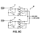
- FIGS. 8A to 8C show circuits of a driving unit 80 in a driving circuit according to a fourth embodiment of the invention.
- the driving unit 80 of this embodiment is almost the same as the driving unit 70 of the third embodiment except that the driving unit 80 has two additional switches 73 and 76 , which are respectively connected to the output terminals and the negative input terminals of the OP amplifiers 11 and 12 .
- the switch 73 or 76 is turned on to function to keep the voltage of the output terminal of the OP amplifier stable when the output terminal of the OP amplifier is cut off.
- FIG. 8A shows the states of the switches when the first output node OUT_ODD outputs the signal of the first OP amplifier 11 and the second output node OUT_EVEN outputs the signal of the second OP amplifier 12 .
- FIG. 8C shows the states of the switches when the first output node OUT_ODD outputs the signal of the second OP amplifier 12 and the second output node OUT_EVEN outputs the signal of the first OP amplifier 11 .
- the switches 71 , 72 , 74 ′ and 75 ′ are turned off while the switch 71 ′, 72 ′, 74 , 75 , 73 and 76 are turned on.
- the driving unit 80 When the driving unit 80 has to be switched from the state of FIG. 8A to the state of FIG. 8C , or from the state of FIG. 8C to the state of FIG. 8A , it has to be switched to the transient state of FIG. 8B , and then to the desired state. That is, the switches 73 and 76 are turned on and other switches are turned off in the transient state, as shown in FIG. 8B .
- the switch is moved to the feedback path of the OP amplifier in the driving unit of the invention, so the output impedance of the driving unit can be greatly reduced, and the time of the stable output voltage of the driving unit can be shortened.
Abstract
Description
Rout=Ron(OP)+Ron(Switch) (1).
Rout′=Ron(OP)+Ron(Switch)/(1+A(op)*B) (2).
Claims (8)
Rout1=Ron1+Ronsw1/(1+Aop1*B),
Rout2=Ron2+Ronsw3/(1+Aop2*B),
Rout1=Ron1+Ronsw1/(1+Aop1*B),
Rout2=Ron1+Ronsw2/(1+Aop1*B),
Rout3=Ron2+Ronsw5/(1+Aop2*B),
Rout4=Ron2+Ronsw6/(1+Aop2*B),
Applications Claiming Priority (3)
| Application Number | Priority Date | Filing Date | Title |
|---|---|---|---|
| TW095100242A TWI342000B (en) | 2006-01-03 | 2006-01-03 | Driving circuit for tft liquid crystal display |
| TW095100242 | 2006-01-03 | ||
| TW95100242A | 2006-01-03 |
Publications (2)
| Publication Number | Publication Date |
|---|---|
| US20070152948A1 US20070152948A1 (en) | 2007-07-05 |
| US8031159B2 true US8031159B2 (en) | 2011-10-04 |
Family
ID=38223837
Family Applications (1)
| Application Number | Title | Priority Date | Filing Date |
|---|---|---|---|
| US11/644,944 Active 2029-07-01 US8031159B2 (en) | 2006-01-03 | 2006-12-26 | Driving circuit for TFT liquid crystal display |
Country Status (2)
| Country | Link |
|---|---|
| US (1) | US8031159B2 (en) |
| TW (1) | TWI342000B (en) |
Cited By (2)
| Publication number | Priority date | Publication date | Assignee | Title |
|---|---|---|---|---|
| US20120319931A1 (en) * | 2011-06-15 | 2012-12-20 | Raydium Semiconductor Corporation | Driving circuit of a display |
| TWI674757B (en) * | 2019-02-13 | 2019-10-11 | 奕力科技股份有限公司 | Buffer circuit |
Families Citing this family (8)
| Publication number | Priority date | Publication date | Assignee | Title |
|---|---|---|---|---|
| KR100926803B1 (en) * | 2007-10-05 | 2009-11-12 | 주식회사 실리콘웍스 | Display driving integrated circuit and display driving system |
| CN101409053B (en) * | 2007-10-11 | 2011-03-16 | 联咏科技股份有限公司 | Drive device as well as system and method thereof |
| JP4466735B2 (en) * | 2007-12-28 | 2010-05-26 | ソニー株式会社 | SIGNAL LINE DRIVE CIRCUIT, DISPLAY DEVICE, AND ELECTRONIC DEVICE |
| US20100033411A1 (en) * | 2008-08-05 | 2010-02-11 | Ching-Chung Lee | Source driver with plural-feedback-loop output buffer |
| TWI452833B (en) * | 2009-12-30 | 2014-09-11 | Ind Tech Res Inst | Output stage, calibration and control method of signal slew rate and control method of signal amplitude |
| TWI456892B (en) * | 2011-06-02 | 2014-10-11 | Fitipower Integrated Tech Inc | Negative feedback circuit and stability increase method thereof and source driver with the negative feedback circuit and control method thereof |
| KR20130139586A (en) * | 2012-06-13 | 2013-12-23 | 삼성전자주식회사 | Output buffer circuit, devices including the same, and operating method thereof |
| TWI630791B (en) * | 2017-09-22 | 2018-07-21 | 奇景光電股份有限公司 | Channel operational amplifier and method for a channel operational amplifier |
Citations (1)
| Publication number | Priority date | Publication date | Assignee | Title |
|---|---|---|---|---|
| US20020190971A1 (en) * | 2001-04-27 | 2002-12-19 | Kabushiki Kaisha Toshiba | Display apparatus, digital-to-analog conversion circuit and digital-to-analog conversion method |
-
2006
- 2006-01-03 TW TW095100242A patent/TWI342000B/en active
- 2006-12-26 US US11/644,944 patent/US8031159B2/en active Active
Patent Citations (1)
| Publication number | Priority date | Publication date | Assignee | Title |
|---|---|---|---|---|
| US20020190971A1 (en) * | 2001-04-27 | 2002-12-19 | Kabushiki Kaisha Toshiba | Display apparatus, digital-to-analog conversion circuit and digital-to-analog conversion method |
Cited By (2)
| Publication number | Priority date | Publication date | Assignee | Title |
|---|---|---|---|---|
| US20120319931A1 (en) * | 2011-06-15 | 2012-12-20 | Raydium Semiconductor Corporation | Driving circuit of a display |
| TWI674757B (en) * | 2019-02-13 | 2019-10-11 | 奕力科技股份有限公司 | Buffer circuit |
Also Published As
| Publication number | Publication date |
|---|---|
| US20070152948A1 (en) | 2007-07-05 |
| TWI342000B (en) | 2011-05-11 |
| TW200727223A (en) | 2007-07-16 |
Similar Documents
| Publication | Publication Date | Title |
|---|---|---|
| US8031159B2 (en) | Driving circuit for TFT liquid crystal display | |
| JP2981883B2 (en) | Driving device for liquid crystal display | |
| US7170351B2 (en) | Differential AB class amplifier circuit and drive circuit using the same | |
| US8031146B2 (en) | Data driver device and display device for reducing power consumption in a charge-share operation | |
| US7911437B1 (en) | Stacked amplifier with charge sharing | |
| US7573333B2 (en) | Amplifier and driving circuit using the same | |
| JP2008122567A (en) | Data driver and display apparatus | |
| JP4408715B2 (en) | Driving circuit and processing circuit | |
| KR20190001563A (en) | Display device, source driving circuit, and control method for source driving circuit | |
| US10621905B2 (en) | Operational amplifier, load driving apparatus and grayscale voltage generating circuit | |
| US7508236B2 (en) | Line driver device | |
| US6313830B1 (en) | Liquid crystal display | |
| TW200620219A (en) | TFT-LCD capable of repairing termination lines | |
| US20060050064A1 (en) | Output devices and display devices utilizing same | |
| US8384641B2 (en) | Amplifier circuit and display device including same | |
| CN113053293A (en) | Shifting register unit, grid driving circuit and display panel | |
| US6559784B1 (en) | Current switching cell for digital to analog converter | |
| US20070236251A1 (en) | Level-shifting apparatus and panel display apparatus using the same | |
| CN100498916C (en) | Drive circuit of liquid crystal display | |
| US7123072B2 (en) | High-accuracy capacitor digital-to-analog converter | |
| US7342452B2 (en) | Control circuit for operational amplifier and method thereof | |
| US20220215864A1 (en) | Buffers and multiplexers | |
| US20080116942A1 (en) | Drive voltage generator | |
| TWI796006B (en) | Source driving circuit and display apparatus | |
| CN211788108U (en) | Source electrode driving device and panel driving system |
Legal Events
| Date | Code | Title | Description |
|---|---|---|---|
| AS | Assignment |
Owner name: SUNPLUS TECHNOLOGY CO., LTD., TAIWAN Free format text: ASSIGNMENT OF ASSIGNORS INTEREST;ASSIGNORS:CHEN, LIN-CHIEN;LIN, KUN-TSUNG;REEL/FRAME:018744/0741 Effective date: 20061127 |
|
| STCF | Information on status: patent grant |
Free format text: PATENTED CASE |
|
| FPAY | Fee payment |
Year of fee payment: 4 |
|
| AS | Assignment |
Owner name: XIAMEN XM-PLUS TECHNOLOGY LTD., CHINA Free format text: ASSIGNMENT OF ASSIGNORS INTEREST;ASSIGNOR:SUNPLUS TECHNOLOGY CO., LTD.;REEL/FRAME:046263/0837 Effective date: 20180628 |
|
| FEPP | Fee payment procedure |
Free format text: ENTITY STATUS SET TO SMALL (ORIGINAL EVENT CODE: SMAL); ENTITY STATUS OF PATENT OWNER: SMALL ENTITY |
|
| MAFP | Maintenance fee payment |
Free format text: PAYMENT OF MAINTENANCE FEE, 8TH YR, SMALL ENTITY (ORIGINAL EVENT CODE: M2552); ENTITY STATUS OF PATENT OWNER: SMALL ENTITY Year of fee payment: 8 |
|
| AS | Assignment |
Owner name: XIAMEN XM-PLUS TECHNOLOGY CO., LTD., CHINA Free format text: CHANGE OF THE NAME AND ADDRESS OF THE ASSIGNEE;ASSIGNOR:XIAMEN XM-PLUS TECHNOLOGY LTD.;REEL/FRAME:061390/0958 Effective date: 20220802 |
|
| MAFP | Maintenance fee payment |
Free format text: PAYMENT OF MAINTENANCE FEE, 12TH YR, SMALL ENTITY (ORIGINAL EVENT CODE: M2553); ENTITY STATUS OF PATENT OWNER: SMALL ENTITY Year of fee payment: 12 |