JP4466735B2 - SIGNAL LINE DRIVE CIRCUIT, DISPLAY DEVICE, AND ELECTRONIC DEVICE - Google Patents
SIGNAL LINE DRIVE CIRCUIT, DISPLAY DEVICE, AND ELECTRONIC DEVICE Download PDFInfo
- Publication number
- JP4466735B2 JP4466735B2 JP2007338996A JP2007338996A JP4466735B2 JP 4466735 B2 JP4466735 B2 JP 4466735B2 JP 2007338996 A JP2007338996 A JP 2007338996A JP 2007338996 A JP2007338996 A JP 2007338996A JP 4466735 B2 JP4466735 B2 JP 4466735B2
- Authority
- JP
- Japan
- Prior art keywords
- output
- operational amplifier
- negative
- output buffer
- positive
- Prior art date
- Legal status (The legal status is an assumption and is not a legal conclusion. Google has not performed a legal analysis and makes no representation as to the accuracy of the status listed.)
- Expired - Fee Related
Links
Images


Classifications
-
- G—PHYSICS
- G09—EDUCATION; CRYPTOGRAPHY; DISPLAY; ADVERTISING; SEALS
- G09G—ARRANGEMENTS OR CIRCUITS FOR CONTROL OF INDICATING DEVICES USING STATIC MEANS TO PRESENT VARIABLE INFORMATION
- G09G3/00—Control arrangements or circuits, of interest only in connection with visual indicators other than cathode-ray tubes
- G09G3/20—Control arrangements or circuits, of interest only in connection with visual indicators other than cathode-ray tubes for presentation of an assembly of a number of characters, e.g. a page, by composing the assembly by combination of individual elements arranged in a matrix no fixed position being assigned to or needed to be assigned to the individual characters or partial characters
- G09G3/34—Control arrangements or circuits, of interest only in connection with visual indicators other than cathode-ray tubes for presentation of an assembly of a number of characters, e.g. a page, by composing the assembly by combination of individual elements arranged in a matrix no fixed position being assigned to or needed to be assigned to the individual characters or partial characters by control of light from an independent source
- G09G3/36—Control arrangements or circuits, of interest only in connection with visual indicators other than cathode-ray tubes for presentation of an assembly of a number of characters, e.g. a page, by composing the assembly by combination of individual elements arranged in a matrix no fixed position being assigned to or needed to be assigned to the individual characters or partial characters by control of light from an independent source using liquid crystals
- G09G3/3611—Control of matrices with row and column drivers
- G09G3/3685—Details of drivers for data electrodes
- G09G3/3688—Details of drivers for data electrodes suitable for active matrices only
-
- G—PHYSICS
- G02—OPTICS
- G02F—OPTICAL DEVICES OR ARRANGEMENTS FOR THE CONTROL OF LIGHT BY MODIFICATION OF THE OPTICAL PROPERTIES OF THE MEDIA OF THE ELEMENTS INVOLVED THEREIN; NON-LINEAR OPTICS; FREQUENCY-CHANGING OF LIGHT; OPTICAL LOGIC ELEMENTS; OPTICAL ANALOGUE/DIGITAL CONVERTERS
- G02F1/00—Devices or arrangements for the control of the intensity, colour, phase, polarisation or direction of light arriving from an independent light source, e.g. switching, gating or modulating; Non-linear optics
- G02F1/01—Devices or arrangements for the control of the intensity, colour, phase, polarisation or direction of light arriving from an independent light source, e.g. switching, gating or modulating; Non-linear optics for the control of the intensity, phase, polarisation or colour
- G02F1/13—Devices or arrangements for the control of the intensity, colour, phase, polarisation or direction of light arriving from an independent light source, e.g. switching, gating or modulating; Non-linear optics for the control of the intensity, phase, polarisation or colour based on liquid crystals, e.g. single liquid crystal display cells
- G02F1/133—Constructional arrangements; Operation of liquid crystal cells; Circuit arrangements
-
- G—PHYSICS
- G09—EDUCATION; CRYPTOGRAPHY; DISPLAY; ADVERTISING; SEALS
- G09G—ARRANGEMENTS OR CIRCUITS FOR CONTROL OF INDICATING DEVICES USING STATIC MEANS TO PRESENT VARIABLE INFORMATION
- G09G3/00—Control arrangements or circuits, of interest only in connection with visual indicators other than cathode-ray tubes
- G09G3/20—Control arrangements or circuits, of interest only in connection with visual indicators other than cathode-ray tubes for presentation of an assembly of a number of characters, e.g. a page, by composing the assembly by combination of individual elements arranged in a matrix no fixed position being assigned to or needed to be assigned to the individual characters or partial characters
-
- G—PHYSICS
- G09—EDUCATION; CRYPTOGRAPHY; DISPLAY; ADVERTISING; SEALS
- G09G—ARRANGEMENTS OR CIRCUITS FOR CONTROL OF INDICATING DEVICES USING STATIC MEANS TO PRESENT VARIABLE INFORMATION
- G09G2310/00—Command of the display device
- G09G2310/02—Addressing, scanning or driving the display screen or processing steps related thereto
- G09G2310/0264—Details of driving circuits
- G09G2310/0281—Arrangement of scan or data electrode driver circuits at the periphery of a panel not inherent to a split matrix structure
-
- G—PHYSICS
- G09—EDUCATION; CRYPTOGRAPHY; DISPLAY; ADVERTISING; SEALS
- G09G—ARRANGEMENTS OR CIRCUITS FOR CONTROL OF INDICATING DEVICES USING STATIC MEANS TO PRESENT VARIABLE INFORMATION
- G09G2310/00—Command of the display device
- G09G2310/02—Addressing, scanning or driving the display screen or processing steps related thereto
- G09G2310/0264—Details of driving circuits
- G09G2310/0297—Special arrangements with multiplexing or demultiplexing of display data in the drivers for data electrodes, in a pre-processing circuitry delivering display data to said drivers or in the matrix panel, e.g. multiplexing plural data signals to one D/A converter or demultiplexing the D/A converter output to multiple columns
-
- G—PHYSICS
- G09—EDUCATION; CRYPTOGRAPHY; DISPLAY; ADVERTISING; SEALS
- G09G—ARRANGEMENTS OR CIRCUITS FOR CONTROL OF INDICATING DEVICES USING STATIC MEANS TO PRESENT VARIABLE INFORMATION
- G09G3/00—Control arrangements or circuits, of interest only in connection with visual indicators other than cathode-ray tubes
- G09G3/20—Control arrangements or circuits, of interest only in connection with visual indicators other than cathode-ray tubes for presentation of an assembly of a number of characters, e.g. a page, by composing the assembly by combination of individual elements arranged in a matrix no fixed position being assigned to or needed to be assigned to the individual characters or partial characters
- G09G3/34—Control arrangements or circuits, of interest only in connection with visual indicators other than cathode-ray tubes for presentation of an assembly of a number of characters, e.g. a page, by composing the assembly by combination of individual elements arranged in a matrix no fixed position being assigned to or needed to be assigned to the individual characters or partial characters by control of light from an independent source
- G09G3/36—Control arrangements or circuits, of interest only in connection with visual indicators other than cathode-ray tubes for presentation of an assembly of a number of characters, e.g. a page, by composing the assembly by combination of individual elements arranged in a matrix no fixed position being assigned to or needed to be assigned to the individual characters or partial characters by control of light from an independent source using liquid crystals
- G09G3/3611—Control of matrices with row and column drivers
- G09G3/3614—Control of polarity reversal in general
Landscapes
- Engineering & Computer Science (AREA)
- Physics & Mathematics (AREA)
- General Physics & Mathematics (AREA)
- Theoretical Computer Science (AREA)
- Computer Hardware Design (AREA)
- Crystallography & Structural Chemistry (AREA)
- Chemical & Material Sciences (AREA)
- Nonlinear Science (AREA)
- Mathematical Physics (AREA)
- Optics & Photonics (AREA)
- Liquid Crystal Display Device Control (AREA)
- Control Of Indicators Other Than Cathode Ray Tubes (AREA)
- Liquid Crystal (AREA)
Description
本発明は、液晶表示装置等のアクティブマトリクス型表示装置における信号線駆動回路および表示装置、並びにそれを用いた電子機器に関するものである。 The present invention relates to a signal line driver circuit and a display device in an active matrix display device such as a liquid crystal display device, and an electronic apparatus using the signal line drive circuit.
画像表示装置、たとえば液晶表示装置などでは、多数の画素をマトリクス状に配列し、表示すべき画像情報に応じて表示セル(画素)毎に光強度を制御することによって画像を表示する。
近年、液晶表示装置の開発、性能の発展はめざましく、テレビジョンや、携帯電話機やPDA(Personal Digital Assistants)などの携帯端末、デジタルカメラ、ノート型パーソナルコンピュータ、ビデオカメラなど、電子機器に入力された映像信号、若しくは、電子機器内で生成した映像信号を、画像若しくは映像として表示するあらゆる分野の電子機器の表示装置に適用することが可能である。
In an image display device such as a liquid crystal display device, a large number of pixels are arranged in a matrix, and an image is displayed by controlling the light intensity for each display cell (pixel) in accordance with image information to be displayed.
In recent years, the development and performance of liquid crystal display devices have been remarkable, and they have been input to electronic devices such as televisions, mobile terminals such as mobile phones and PDAs (Personal Digital Assistants), digital cameras, notebook personal computers, and video cameras. The present invention can be applied to display devices for electronic devices in all fields that display video signals or video signals generated in electronic devices as images or videos.
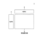
図1は、一般的な液晶表示装置の概略構成を示す図である。 FIG. 1 is a diagram showing a schematic configuration of a general liquid crystal display device.
この液晶表示装置1は、図1に示すように、透明絶縁基板、たとえばガラス基板上に、液晶セルを含む複数の画素がマトリクス状に配置された有効表示部2、信号線を駆動するための信号線駆動回路(水平駆動回路、ソースドライバ:HDRV)3、およびゲート線駆動回路(垂直駆動回路、ゲートドライバ:VDRV)4を有する。
As shown in FIG. 1, the liquid
有効表示部2には、図示しない液晶セルを含む複数の画素がマトリクス状に配列されている。
また、有効表示部2には、信号線駆動回路3、並びにゲート線駆動回路4により駆動される信号線およびゲート線(垂直走査線)がマトリクス状に配線されている。
In the
In the
そして、液晶表示装置においては、液晶分子の劣化を防止するために、液晶に電圧が交流の形態で印加される必要があり、一般的な液晶表示装置では、液晶に交流電圧(コモン電圧)を印加する、コモン一定駆動法またはコモン反転駆動法の、いわゆる極性反転動作法が採用される。 In a liquid crystal display device, it is necessary to apply a voltage to the liquid crystal in the form of an alternating current in order to prevent deterioration of liquid crystal molecules. In a general liquid crystal display device, an alternating voltage (common voltage) is applied to the liquid crystal. The so-called polarity reversal operation method of the common constant drive method or the common reversal drive method to be applied is adopted.
コモン一定駆動法では、対向電極の電圧を一定レベルに固定したままで、画素電極に対向電極電圧に対して正の極性を有する電圧と負の極性を有する電圧を交互に印加する。 In the common constant drive method, a voltage having a positive polarity and a voltage having a negative polarity with respect to the counter electrode voltage are alternately applied to the pixel electrode while the voltage of the counter electrode is fixed at a constant level.
コモン反転駆動法は、対向電極の電圧を高レベルと低レベルとの間で反転させながら画素電極に対向電極電圧に対して正の極性を有する電圧と負の極性を有する電圧を交互に印加する。
この場合、対向電極の電圧が高レベルのときに画素電極にはこの高レベルを基準として負の極性を有する電圧が印加され、対向電極の電圧が低レベルのときに画素電極にはこの低レベルの基準として正の極性を有する電圧が印加されることになる。
In the common inversion driving method, a voltage having a positive polarity and a voltage having a negative polarity with respect to the counter electrode voltage are alternately applied to the pixel electrode while inverting the voltage of the counter electrode between a high level and a low level. .
In this case, a voltage having a negative polarity with respect to the high level is applied to the pixel electrode when the voltage of the counter electrode is high, and this low level is applied to the pixel electrode when the voltage of the counter electrode is low. As a reference, a voltage having a positive polarity is applied.
この極性反転動作に対応して信号線駆動回路3の出力バッファ部が構成される。
信号線駆動回路3において、極性反転動作を行わせるため、出力バッファ部にレイルトゥレイル(Rail to Rail)の出力アナログバッファ回路を用いたり(非特許文献1参照)、スイッチを有する出力セレクタを用いた構成が採用されてきた(特許文献1参照)。
The output buffer section of the signal
In the signal
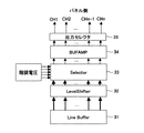
図2は、出力セレクタを用いた従来の信号線駆動回路の構成例を示すブロック図である。 FIG. 2 is a block diagram showing a configuration example of a conventional signal line driving circuit using an output selector.
この信号線駆動回路3は、パラレルシリアル変換された信号線を駆動するための駆動データが格納されるラインバッファと、ラインバッファ31のデータのレベルを駆動レベルに応じたレベルに変換するレベルシフタ32と、階調電圧を受けて駆動データをデジタルデータからアナログデータに変換するデジタルアナログコンバータ(DAC)を複数含むセレクタ部33と、セレクタ部33から出力された駆動データを増幅し、正極性の信号電圧および負極性の信号電圧を生成するするバッファアンプ部34と、互いに隣接する信号線に正極性の信号電圧および負極性の信号電圧を選択的に供給する出力セレクタ35と、を有する。
The signal
図3は、図2のバッファアンプ部と出力セレクタとの構成例を示す図である。
図3においては、隣接する2チャネル分に対応する信号線駆動回路の出力バッファ段を示している。実際には、アナログバッファのチャネル数は数100以上あり、これらのチャネルに対応する信号線が駆動される。
FIG. 3 is a diagram illustrating a configuration example of the buffer amplifier unit and the output selector of FIG.
FIG. 3 shows an output buffer stage of the signal line driver circuit corresponding to two adjacent channels. Actually, the number of channels of the analog buffer is several hundreds or more, and signal lines corresponding to these channels are driven.
図3に示すバッファアンプ部34は、チャネルCH1に接続される信号線SGL1およびチャネルCH2に接続される信号線SGL2に正極性の信号電圧を供給する第1の増幅回路34−1と、信号線SGL1および信号線SGL2に負極性の信号電圧を供給する第2の増幅回路34−2と、を有する。 3 includes a first amplifier circuit 34-1 for supplying a positive signal voltage to the signal line SGL1 connected to the channel CH1 and the signal line SGL2 connected to the channel CH2, and the signal line. A second amplifier circuit 34-2 for supplying a negative signal voltage to the SGL1 and the signal line SGL2.
第1の増幅回路34−1は、前段のDAC出力に対して縦続接続された演算増幅器(OTA:Operational Transconductance Amplifier)34−11と出力増幅器(OAMP)34−12とにより構成されている。
OTA34−11の反転入力端子(−)が前段のDACの出力線に接続され、非反転入力端子(+)がOAMP34−12の出力に接続されている。
The first amplifier circuit 34-1 includes an operational amplifier (OTA) 34-11 and an output amplifier (OAMP) 34-12 that are cascade-connected to the DAC output of the previous stage.
The inverting input terminal (−) of the OTA 34-11 is connected to the output line of the preceding DAC, and the non-inverting input terminal (+) is connected to the output of the OAMP 34-12.
第1の増幅回路34−2は、前段のDAC出力に対して縦続接続されたOTA34−21とOAMP34−22とにより構成されている。
OTA34−21の反転入力端子(−)が前段のDACの出力線に接続され、非反転入力端子(+)がOAMP34−22の出力に接続されている。
The first amplifier circuit 34-2 includes an OTA 34-21 and an OAMP 34-22 that are cascade-connected to the DAC output of the previous stage.
The inverting input terminal (−) of the OTA 34-21 is connected to the output line of the preceding DAC, and the non-inverting input terminal (+) is connected to the output of the OAMP 34-22.
出力セレクタ35は、第1のスイッチ群35−1および第2のスイッチ群35−2を有している。
The
第1のスイッチ群35−1は、信号STRでオン、オフが制御されるスイッチSW11と、信号SRSでオン、オフが制御されるスイッチSW12と、を有する。スイッチSW11とスイッチSW12とは相補的にオン、オフされる。
スイッチSW11の端子aが第1の増幅回路34−1のOAMP34−12の出力に接続され、端子bがチャネルCH1の信号線SGL1に接続されている。
スイッチSW12の端子aが第1の増幅回路34−1のOAMP34−12の出力に接続され、端子bがチャネルCH2の信号線SGL2に接続されている。
The first switch group 35-1 includes a switch SW11 whose on / off is controlled by a signal STR and a switch SW12 whose on / off is controlled by a signal SRS. The switches SW11 and SW12 are turned on and off in a complementary manner.
The terminal a of the switch SW11 is connected to the output of the OAMP 34-12 of the first amplifier circuit 34-1, and the terminal b is connected to the signal line SGL1 of the channel CH1.
The terminal a of the switch SW12 is connected to the output of the OAMP 34-12 of the first amplifier circuit 34-1, and the terminal b is connected to the signal line SGL2 of the channel CH2.
第2のスイッチ群35−2は、信号STRでオン、オフが制御されるスイッチSW21と、信号SRSでオン、オフが制御されるスイッチSW22と、を有する。スイッチSW21とスイッチSW22とは相補的にオン、オフされる。
スイッチSW21の端子aが第2の増幅回路34−2のOAMP34−22の出力に接続され、端子bがチャネルCH2の信号線SGL2に接続されている。
スイッチSW22の端子aが第2の増幅回路34−2のOAMP34−22の出力に接続され、端子bがチャネルCH1の信号線SGL1に接続されている。
The second switch group 35-2 includes a switch SW21 whose on / off is controlled by a signal STR and a switch SW22 whose on / off is controlled by a signal SRS. The switches SW21 and SW22 are turned on and off in a complementary manner.
The terminal a of the switch SW21 is connected to the output of the OAMP 34-22 of the second amplifier circuit 34-2, and the terminal b is connected to the signal line SGL2 of the channel CH2.
The terminal a of the switch SW22 is connected to the output of the OAMP 34-22 of the second amplifier circuit 34-2, and the terminal b is connected to the signal line SGL1 of the channel CH1.
このような構成において、出力セレクタ35のスイッチSW11とスイッチSW21がオン状態、スイッチSW12とスイッチSW22がオフ状態に制御されると、第1の増幅回路34−1による正極性の信号電圧が信号線SGL1に供給され、第2の増幅回路34−2により負極性の信号電圧が信号線SGL2に供給される。
一方、出力セレクタ35のスイッチSW12とスイッチSW22がオン状態、スイッチSW11とスイッチSW21がオフ状態に制御されると、第1の増幅回路34−1による正極性の信号電圧が信号線SGL2に供給され、第2の増幅回路34−2により負極性の信号電圧が信号線SGL1に供給される。
On the other hand, when the switches SW12 and SW22 of the
上述したように、液晶表示装置においては、極性反転動作を行わせるため、Rail−To−Railの出力バッファ回路が用いられたり、あるいは図2および図3に示すような出力セレクタを用いることで極性反転を実現していた。 As described above, in the liquid crystal display device, a Rail-To-Rail output buffer circuit is used to perform the polarity inversion operation, or the output selector as shown in FIGS. The reversal was realized.
ところが、前者のRail−To−Railの出力バッファ回路では、次にあげるような問題がある。
すなわち、回路構成が複雑になり、消費電力が大きく、レイアウト面積が大きい。
However, the former Rail-To-Rail output buffer circuit has the following problems.
That is, the circuit configuration is complicated, power consumption is large, and the layout area is large.
また、後者の出力セレクタを用いる場合においては、回路構成の複雑化、消費電力の低減を図ることはできが、次にあげる問題がある。
ON抵抗を小さくするため、出力セレクタサイズと出力段のサイズが大きくなる。その結果、レイアウト面積の増加を招く。
また、出力セレクタのON抵抗によるセトリングの低下を招く。
When the latter output selector is used, the circuit configuration can be complicated and the power consumption can be reduced, but there are the following problems.
In order to reduce the ON resistance, the output selector size and the output stage size are increased. As a result, the layout area increases.
In addition, settling is reduced due to the ON resistance of the output selector.
アナログバッファのCH数は数100以上あり、CH数の多い高精細な用途にはレイアウト面積の削減が強く要求され、加えて近年の高精細化にともない動作周波数の高速化が課題となっている。 The number of CHs in an analog buffer is several hundreds or more, and a high-definition application with a large number of CHs is strongly required to reduce the layout area, and in addition, there is a problem of increasing the operating frequency with the recent increase in definition. .
本発明は、回路構成の複雑化、消費電流の増加、特性低下を防止することができ、素子サイズ(レイアウト面積)の削減を図ることが可能な信号線駆動回路および表示装置、並びにそれを用いた電子機器を提供することにある。 The present invention can prevent a complicated circuit configuration, an increase in current consumption, and a characteristic deterioration, and a signal line driver circuit and a display device capable of reducing the element size (layout area), and the same. Is to provide the electronic equipment that was.
上記目的を達成するため、本発明の第1の観点は、極性反転駆動される表示セルがマトリクス状に配置され、当該極性反転に対応して上記表示セルに接続される信号線に正極性の信号電圧または負極性の信号電圧を供給する信号線駆動回路であって、信号線を駆動する入力データを増幅し、正極性の信号電圧および負極性の信号電圧を生成し、対をなす第1の信号線および第2の信号線に正極性の信号電圧および負極性の信号電圧を選択的に供給する出力バッファ部を有し、上記出力バッファ部は、入力データを増幅し、正極性の信号電圧を生成する正極性側演算増幅器と、入力データを増幅し、負極性の信号電圧を生成する負極性側演算増幅器と、上記第1の信号線に正極性または負極性の信号電圧を供給する第1の出力バッファと、上記第2の信号線に負極性または正極性の信号電圧を供給する第2の出力バッファと、上記正極性側演算増幅器の出力および上記負極性側演算増幅器の出力の各々と、上記第1の出力バッファの入力および上記第2の出力バッファの入力の各々との間、並びに、上記正極性側演算増幅器および上記負極性側演算増幅器の帰還入力段に配置されたスイッチ群と、を含み、上記スイッチ群は、第1のモード時は、上記正極性側演算増幅器で生成された正極性の信号電圧を上記第1の出力バッファに入力し、当該第1の出力バッファの出力を上記正極性側演算増幅器に帰還させ、上記負極性側演算増幅器で生成された負極性の信号電圧を上記第2の出力バッファに入力し、当該第2の出力バッファの出力を上記負極性側演算増幅器に帰還させ、第2のモード時は、上記正極性側演算増幅器で生成された正極性の信号電圧を上記第2の出力バッファに入力し、当該第2の出力バッファの出力を上記正極性側演算増幅器に帰還させ、上記負極性側演算増幅器で生成された負極性の信号電圧を上記第1の出力バッファに入力し、当該第1の出力バッファの出力を上記負極性側演算増幅器に帰還させ、上記第1の出力バッファの出力と上記第1の信号線との間、並びに上記第2の出力バッファの出力と上記第2の信号線との間には、スイッチが介在しない。 In order to achieve the above object, according to a first aspect of the present invention, display cells to be polarity-inverted are arranged in a matrix, and signal lines connected to the display cells corresponding to the polarity inversion have a positive polarity. A signal line driving circuit that supplies a signal voltage or a negative signal voltage, amplifies input data for driving the signal line, generates a positive signal voltage and a negative signal voltage, and forms a pair. And an output buffer unit that selectively supplies a positive signal voltage and a negative signal voltage to the second signal line and the second signal line. The output buffer unit amplifies the input data to generate a positive signal. A positive polarity operational amplifier for generating a voltage; a negative polarity operational amplifier for amplifying input data to generate a negative signal voltage; and supplying a positive or negative signal voltage to the first signal line. A first output buffer and the above A second output buffer for supplying a negative or positive signal voltage to two signal lines, each of an output of the positive polarity side operational amplifier and an output of the negative polarity side operational amplifier, and the first output buffer And a switch group disposed in the feedback input stage of the positive polarity side operational amplifier and the negative polarity side operational amplifier, and the switch group. In the first mode, the positive polarity signal voltage generated by the positive polarity side operational amplifier is input to the first output buffer, and the output of the first output buffer is input to the positive polarity side operational amplifier. The negative signal voltage generated by the negative polarity side operational amplifier is input to the second output buffer, the output of the second output buffer is fed back to the negative polarity side operational amplifier, 2 At the time of input, the positive polarity signal voltage generated by the positive polarity side operational amplifier is input to the second output buffer, and the output of the second output buffer is fed back to the positive polarity side operational amplifier. The negative signal voltage generated by the negative side operational amplifier is input to the first output buffer, the output of the first output buffer is fed back to the negative side operational amplifier, and the first output buffer No switch is interposed between the output of the second output buffer and the first signal line, and between the output of the second output buffer and the second signal line.
好適には、上記正極性側演算増幅器は、第1導電型トランジスタの差動対を有し、上記負極性側演算増幅器は、第2導電型トランジスタの差動対を有し、上記第1および第2の出力バッファは、AB級プシュプル動作機能を有する。 Preferably, the positive polarity side operational amplifier has a differential pair of first conductivity type transistors, and the negative polarity side operational amplifier has a differential pair of second conductivity type transistors. The second output buffer has a class AB push-pull operation function.
好適には、上記第1および第2の出力バッファは、2つの入力端子を有する。 Preferably, the first and second output buffers have two input terminals.
本発明の第2の観点の表示装置は、極性反転駆動される表示セルがマトリクス状に配置される表示部と、上記極性反転に対応して上記表示セルに接続される信号線に正極性の信号電圧または負極性の信号電圧を供給する信号線駆動回路と、を有し、上記信号線駆動回路は、信号線を駆動する入力データを増幅し、正極性の信号電圧および負極性の信号電圧を生成し、対をなす第1の信号線および第2の信号線に正極性の信号電圧および負極性の信号電圧を選択的に供給する出力バッファ部を含み、上記出力バッファ部は、入力データを増幅し、正極性の信号電圧を生成する正極性側演算増幅器と、入力データを増幅し、負極性の信号電圧を生成する負極性側演算増幅器と、上記第1の信号線に正極性または負極性の信号電圧を供給する第1の出力バッファと、上記第2の信号線に負極性または正極性の信号電圧を供給する第2の出力バッファと、上記正極性側演算増幅器の出力および上記負極性側演算増幅器の出力の各々と、上記第1の出力バッファの入力および上記第2の出力バッファの入力の各々との間、並びに、上記正極性側演算増幅器および上記負極性側演算増幅器の帰還入力段に配置されたスイッチ群と、を含み、上記スイッチ群は、第1のモード時は、上記正極性側演算増幅器で生成された正極性の信号電圧を上記第1の出力バッファに入力し、当該第1の出力バッファの出力を上記正極性側演算増幅器に帰還させ、上記負極性側演算増幅器で生成された負極性の信号電圧を上記第2の出力バッファに入力し、当該第2の出力バッファの出力を上記負極性側演算増幅器に帰還させ、第2のモード時は、上記正極性側演算増幅器で生成された正極性の信号電圧を上記第2の出力バッファに入力し、当該第2の出力バッファの出力を上記正極性側演算増幅器に帰還させ、上記負極性側演算増幅器で生成された負極性の信号電圧を上記第1の出力バッファに入力し、当該第1の出力バッファの出力を上記負極性側演算増幅器に帰還させ、上記第1の出力バッファの出力と上記第1の信号線との間、並びに上記第2の出力バッファの出力と上記第2の信号線との間には、スイッチが介在しない。 According to a second aspect of the present invention, there is provided a display device in which display cells driven in polarity inversion are arranged in a matrix, and signal lines connected to the display cells corresponding to the polarity inversion are positive. A signal line driving circuit for supplying a signal voltage or a negative signal voltage, the signal line driving circuit amplifying input data for driving the signal line, and a positive signal voltage and a negative signal voltage generate, it includes selectively supplying the output buffer unit a first signal line and second signal lines to the signal voltage of positive polarity and negative polarity of the signal voltage of the pair, the output buffer section, input data A positive-polarity operational amplifier that generates a positive-polarity signal voltage, a negative-polarity-side operational amplifier that amplifies input data and generates a negative-polarity signal voltage, and a positive polarity or First to supply a negative signal voltage A power buffer, a second output buffer that supplies a negative or positive signal voltage to the second signal line, each of an output of the positive polarity side operational amplifier and an output of the negative polarity side operational amplifier, A switch group disposed between each of the input of the first output buffer and the input of the second output buffer, and in a feedback input stage of the positive polarity side operational amplifier and the negative polarity side operational amplifier; In the first mode, the switch group inputs the positive signal voltage generated by the positive operational amplifier to the first output buffer, and outputs the output of the first output buffer. The negative-polarity operational amplifier is fed back, the negative signal voltage generated by the negative-polarity operational amplifier is input to the second output buffer, and the output of the second output buffer is input to the negative-polarity operational amplifier. amplifier In the second mode, the positive signal voltage generated by the positive operational amplifier is input to the second output buffer, and the output of the second output buffer is input to the positive arithmetic A negative polarity signal voltage generated by the negative polarity side operational amplifier is input to the first output buffer, and an output of the first output buffer is fed back to the negative polarity side operational amplifier. There are no switches between the output of the first output buffer and the first signal line, and between the output of the second output buffer and the second signal line.
本発明の第3の観点は、表示装置を有する電子機器であって、上記表示装置は、極性反転駆動される表示セルがマトリクス状に配置される表示部と、上記極性反転に対応して上記表示セルに接続される信号線に正極性の信号電圧または負極性の信号電圧を供給する信号線駆動回路と、を有し、上記信号線駆動回路は、信号線を駆動する入力データを増幅し、正極性の信号電圧および負極性の信号電圧を生成し、対をなす第1の信号線および第2の信号線に正極性の信号電圧および負極性の信号電圧を選択的に供給する出力バッファ部を含み、上記出力バッファ部は、入力データを増幅し、正極性の信号電圧を生成する正極性側演算増幅器と、入力データを増幅し、負極性の信号電圧を生成する負極性側演算増幅器と、上記第1の信号線に正極性または負極性の信号電圧を供給する第1の出力バッファと、上記第2の信号線に負極性または正極性の信号電圧を供給する第2の出力バッファと、上記正極性側演算増幅器の出力および上記負極性側演算増幅器の出力の各々と、上記第1の出力バッファの入力および上記第2の出力バッファの入力の各々との間、並びに、上記正極性側演算増幅器および上記負極性側演算増幅器の帰還入力段に配置されたスイッチ群と、を含み、上記スイッチ群は、第1のモード時は、上記正極性側演算増幅器で生成された正極性の信号電圧を上記第1の出力バッファに入力し、当該第1の出力バッファの出力を上記正極性側演算増幅器に帰還させ、上記負極性側演算増幅器で生成された負極性の信号電圧を上記第2の出力バッファに入力し、当該第2の出力バッファの出力を上記負極性側演算増幅器に帰還させ、第2のモード時は、上記正極性側演算増幅器で生成された正極性の信号電圧を上記第2の出力バッファに入力し、当該第2の出力バッファの出力を上記正極性側演算増幅器に帰還させ、上記負極性側演算増幅器で生成された負極性の信号電圧を上記第1の出力バッファに入力し、当該第1の出力バッファの出力を上記負極性側演算増幅器に帰還させ、上記第1の出力バッファの出力と上記第1の信号線との間、並びに上記第2の出力バッファの出力と上記第2の信号線との間には、スイッチが介在しない。 According to a third aspect of the present invention, there is provided an electronic apparatus having a display device, wherein the display device includes a display unit in which display cells driven in polarity inversion are arranged in a matrix, and the display unit corresponding to the polarity inversion. A signal line driver circuit that supplies a positive signal voltage or a negative signal voltage to a signal line connected to the display cell, and the signal line driver circuit amplifies input data for driving the signal line. , generates a signal voltage of positive polarity and negative polarity of the signal voltage, pair of first signal lines and second signal lines to selectively supply the output buffer signal voltage of positive polarity and negative polarity of the signal voltage forming the The output buffer unit amplifies input data and generates a positive signal voltage, and a negative polarity side operational amplifier that amplifies input data and generates a negative signal voltage And a positive electrode on the first signal line Alternatively, a first output buffer that supplies a negative signal voltage, a second output buffer that supplies a negative or positive signal voltage to the second signal line, and an output of the positive-side operational amplifier; Between each of the outputs of the negative polarity side operational amplifier and each of the inputs of the first output buffer and the second output buffer, and the positive polarity side operational amplifier and the negative polarity side operational amplifier. And a switch group disposed in the feedback input stage, and in the first mode, the switch group receives the positive polarity signal voltage generated by the positive polarity side operational amplifier in the first output buffer. The output of the first output buffer is fed back to the positive operational amplifier, and the negative signal voltage generated by the negative operational amplifier is input to the second output buffer, 2 out The output of the buffer is fed back to the negative polarity side operational amplifier, and in the second mode, the positive polarity signal voltage generated by the positive polarity side operational amplifier is input to the second output buffer, and the second output buffer The output of the output buffer is fed back to the positive operational amplifier, the negative signal voltage generated by the negative operational amplifier is input to the first output buffer, and the output of the first output buffer is output. Is fed back to the negative-side operational amplifier, between the output of the first output buffer and the first signal line, and between the output of the second output buffer and the second signal line. There is no intervening switch.
本発明によれば、たとえば第1のモード時には、正極性側演算増幅器による正極性の信号電圧が第1の出力バッファを介して第1の信号線に供給され、負極性側演算増幅器による負極性の信号電圧が第2の出力バッファを介して第2の信号線に供給される。
一方、第2のモード時には、正極性側演算増幅器による正極性の信号電圧が第2の出力バッファを介して第2の信号線に供給され、負極性側演算増幅器による負極性の信号電圧が第1の出力バッファを介して第1の信号線に供給される。
According to the present invention, for example, in the first mode, the positive signal voltage from the positive operational amplifier is supplied to the first signal line via the first output buffer, and the negative signal from the negative operational amplifier is supplied. Is supplied to the second signal line via the second output buffer.
On the other hand, in the second mode, a positive signal voltage from the positive operational amplifier is supplied to the second signal line via the second output buffer, and a negative signal voltage from the negative operational amplifier is supplied to the second signal line. The signal is supplied to the first signal line through one output buffer.
本発明によれば、回路構成の複雑化、消費電流の増加、特性低下を防止することができ、素子サイズ(レイアウト面積)の削減を図ることができる。
また、本発明において出力段増幅器のオフセットキャンセル効果も発生するため、画質向上にも貢献することになる。
According to the present invention, it is possible to prevent a complicated circuit configuration, an increase in current consumption, and a characteristic deterioration, and it is possible to reduce the element size (layout area).
Further, in the present invention, the offset canceling effect of the output stage amplifier is also generated, which contributes to the improvement of the image quality.
以下、本発明の実施の形態について図面に関連付けて詳細に説明する。 Hereinafter, embodiments of the present invention will be described in detail with reference to the drawings.
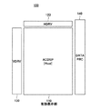
図4は、本発明の実施形態に係る表示装置の構成例を示す図である。
ここでは、たとえば、各画素の電気光学素子として液晶セルを用いたアクティブマトリクス型液晶表示装置に適用した場合を例に採って説明する。
FIG. 4 is a diagram illustrating a configuration example of the display device according to the embodiment of the present invention.
Here, for example, a case where the present invention is applied to an active matrix type liquid crystal display device using a liquid crystal cell as an electro-optical element of each pixel will be described.
この液晶表示装置100は、図4に示すように、透明絶縁基板、たとえばガラス基板上に、液晶セルを含む複数の画素がマトリクス状に配置された有効表示部(ACDSP)110、信号線を駆動するための信号線駆動回路(水平駆動回路、ソースドライバ:HDRV)120、液晶セルを走査し選択するためのゲート線(走査線)を駆動するゲート線駆動回路(垂直駆動回路、ゲートドライバ)130、およびデータ処理回路(DATAPRC)140を有する。
As shown in FIG. 4, the liquid
以下、本実施形態の液晶表示装置100の各構成要素の構成並びに機能について順を追って説明する。
Hereinafter, the configuration and function of each component of the liquid
有効表示部(以下、単に表示部という)110は、液晶セルを含む複数の画素がマトリクス状に配列されている。
そして、有効表示部110は、信号線駆動回路120、並びにゲート線駆動回路130により駆動される信号線(データ線)およびゲート線(垂直走査線)がマトリクス状(格子状)に配線されている。
In an effective display portion (hereinafter simply referred to as a display portion) 110, a plurality of pixels including liquid crystal cells are arranged in a matrix.
In the
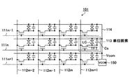
図5は、表示部110の具体的な構成の一例を示す図である。
ここでは、図面の簡略化のために、3行(n−1行〜n+1行)4列(m−2列〜m+1列)の画素配列の場合を例に採って示している。
FIG. 5 is a diagram illustrating an example of a specific configuration of the
Here, for simplification of the drawing, the case of a pixel array of 3 rows (n−1 rows to n + 1 rows) and 4 columns (m−2 columns to m + 1 columns) is shown as an example.
図5において、表示部110には、ゲート線(垂直走査線)…,111n−1,111n,111n+1,…と、信号線(データ線)…,112m−2,112m−1,112m,112m+1,…とがマトリクス状に配線され、それらの交点部分に単位画素113が配置されている。
5, the
単位画素113は、画素トランジスタである薄膜トランジスタTFT(Thin Film Transistor)、液晶セルLCおよび保持容量Csを有する構成となっている。
ここで、液晶セルLCは、薄膜トランジスタTFTで形成される画素電極(一方の電極)とこれに対向して形成される対向電極(他方の電極)との間で発生する容量を意味する。
The unit pixel 113 includes a thin film transistor TFT (Thin Film Transistor) that is a pixel transistor, a liquid crystal cell LC, and a storage capacitor Cs.
Here, the liquid crystal cell LC means a capacitance generated between a pixel electrode (one electrode) formed by a thin film transistor TFT and a counter electrode (the other electrode) formed opposite thereto.
薄膜トランジスタTFTは、ゲート電極がゲート線(垂直走査線)…,111n−1,111n,111n+1,…に接続され、ソース電極が信号線…,112m−2,112m−1,112m,112m+1,…に接続されている。
液晶セルLCは、画素電極が薄膜トランジスタTFTのドレイン電極に接続され、対向電極が共通線114に接続されている。保持容量Csは、薄膜トランジスタTFTのドレイン電極と共通線114との間に接続されている。
共通線114には、コモン電圧供給回路(VCOM回路)150により所定の交流電圧がコモン電圧Vcomとして与えられる。
The thin film transistor TFT has a gate electrode connected to a gate line (vertical scanning line)..., 111n−1, 111n, 111n + 1,..., And a source electrode connected to a signal line..., 112m−2, 112m−1, 112m, 112m + 1,. It is connected.
In the liquid crystal cell LC, the pixel electrode is connected to the drain electrode of the thin film transistor TFT, and the counter electrode is connected to the
A predetermined AC voltage is applied to the
ゲート線(垂直走査線)…,111n−1,111n,111n+1,…の各一端は、図4に示すゲート線駆動回路130の対応する行の各出力端にそれぞれ接続される。
ゲート線駆動回路130は、たとえばシフトレジスタを含んで構成され、垂直転送クロックVCK(図示せず)に同期して順次垂直選択パルスを発生してゲート線(垂直走査線)…,111n−1,111n,111n+1,…に与えることによって垂直走査を行う。
.., 111n−1, 111n, 111n + 1,... Are connected to output terminals of the corresponding row of the gate
The gate
また、表示部110において、たとえば、信号線…,112m−1,112m+1,…の各一端が図4に示す信号線駆動回路120の対応する列の各出力端に接続される。
In the
信号線駆動回路120は、駆動レベルに応じたレベルに変換された信号線を駆動するための駆動データを、階調電圧に応じてデジタルデータからアナログデータに変換し、アナログ駆動データを増幅し、正極性の信号電圧および負極性の信号電圧を生成する機能を有し、さらに、互いに隣接する信号線に正極性の信号電圧および負極性の信号電圧を選択的に供給する機能を有している。
The signal
データ処理回路140は、たとえば外部より入力されたパラレルのデータのレベルを所定レベルにシフトするレベルシフタや、レベルシフトされたデータを位相調整や周波数を下げるために、シリアルデータからパラレルデータに変換するシリアル・パラレルコンバータを含み、パラレルデータを信号線駆動回路120に出力する。
The
以下、本実施形態に係る信号線駆動回路120の構成および機能について具体的に説明する。
Hereinafter, the configuration and function of the signal
図6は、本実施形態に係る信号線駆動回路の構成例を示すブロック図である。 FIG. 6 is a block diagram illustrating a configuration example of the signal line driving circuit according to the present embodiment.
図6に示す信号線駆動回路120は、シフトレジスタ121、データラッチ部122、DAC(デジタル・アナログコンバータ)123、および出力バッファ部124を有する。
なお、図6において、符号141で示すシリアル・パラレルコンバータ(SPC)は、データ処理回路141に含まれる。
The signal
In FIG. 6, a serial / parallel converter (SPC) denoted by
シフトレジスタ121は、水平転送クロックHCK(図示せず)に同期して各列に対応する各転送段から順次シフトパルス(サンプリングパルス)をデータラッチ部122に出力する。
The
データラッチ部122は、シリアル・パラレルコンバータ141による信号線を駆動するためのデジタル駆動データを、シフトレジスタ121によるサンプリングパルスで順次サンプリングしてラッチする。
The data latch
DAC123は、階調電圧を受けて駆動データをデジタルデータからアナログデータに変換する。
The
出力バッファ部124は、DAC123から出力されたアナログ駆動データを増幅し、正極性の信号電圧および負極性の信号電圧を生成し、かつ、対をなす互いに隣接する信号線112に正極性の信号電圧および負極性の信号電圧を選択的に供給する。
The
図7は、本実施形態に係る信号線駆動回路における出力バッファ部の構成例を示す図である。
以下の説明では、出力バッファ部124に符号200を付して説明する。
FIG. 7 is a diagram illustrating a configuration example of the output buffer unit in the signal line driving circuit according to the present embodiment.
In the following description, the
図7に示す出力バッファ部200は、前段のDAC123の出力に対して接続され入力データを増幅し、正極性の信号電圧を生成する機能を有する正極性側演算増幅器(OTA:Operational Transconductance Amplifier)211と、出力バッファとしての機能を有し、チャネルCHm(たとえばm=1)に接続される第1の信号線112mに正極性または負極性の信号電圧を供給する第1の共通出力増幅器(OAMP)212と、前段のDAC123の出力に対して接続され入力データを増幅し、負正極性の信号電圧を生成する機能を有する負極性側OTA221と、出力バッファとしての機能を有し、チャネルCHm+1(たとえばCH2)に接続される第2の信号線112m+1に負極性または正極性の信号電圧を供給する第2のOAMP222と、正極性側OTA211の出力および負極性側OTA221の出力の各々と、第1のOAMP212の入力および第2のOAMP222の入力の各々との間、並びに、正極性側OTA211および負極性側OTA221の帰還入力段に第1のスイッチSW231〜第8のスイッチSW238を含むスイッチ群230と、を有する。
The output buffer unit 200 shown in FIG. 7 is connected to the output of the
正極性側OTA211の出力は、スイッチSW231を介して第1のOAMP212の入力に供給され、スイッチSW232を介して第2のOAMP222の入力に供給される。
負極性側OTA221の出力は、スイッチSW233を介して第2のOAMP222の入力に供給され、スイッチSW234を介して第1のOAMP212の入力に供給される。
The output of the positive
The output of the negative
正極性側OTA211の反転入力端子(−)が前段のDAC123の出力線が接続される入力端子TI1に接続され、非反転入力端子(+)がスイッチSW235を介して第1のOAMP212の出力端子に接続され、スイッチSW236を介して第2のOAMP222の出力端子に接続されている。
The inverting input terminal (−) of the positive
負極性側OTA221の反転入力端子(−)が前段のDAC123の出力線が接続される入力端子TI2に接続され、非反転入力端子(+)がスイッチSW237を介して第2のOAMP222の出力端子に接続され、スイッチSW238を介して第1のOAMP212の出力端子に接続されている。
The inverting input terminal (−) of the negative
第1のOAMP212の出力端子は、チャネルCH1の第1の信号線112mに接続される出力端子TO1に接続されている。
第2のOAMP222の出力端子は、チャネルCH2の第2の信号線112m+1に接続される出力端子TO2に接続されている。
The output terminal of the
The output terminal of the
スイッチ群230において、スイッチSW231、SW233、SW235、SW237は共通の信号STRでオン、オフが制御され、これらスイッチにより第1のスイッチ群が構成される。
また、スイッチSW232、SW234、SW236、SW238は共通の信号CRSでオン、オフが制御され、これらスイッチにより第2のスイッチ群が構成される。
第1のスイッチ群のスイッチSW231、SW233、SW235、SW237と第2のスイッチ群のスイッチSW232、SW234、SW236、SW238は相補的にオン、オフされる。
図示しない制御系により、信号STRがハイレベルのとき、信号CRSはローレベルに制御され、信号STRがローレベルのとき、信号CRSはハイレベルに制御される。
たとえば、第1のスイッチ群のスイッチSW231、SW233、SW235、SW237は信号STRがハイレベルのときオンし、ローレベルのときオフする。
第2のスイッチ群のスイッチSW232、SW234、SW236、SW238は信号CRSがハイレベルのときオンし、ローレベルのときオフする。
In the
The switches SW232, SW234, SW236, and SW238 are controlled to be turned on and off by a common signal CRS, and a second switch group is configured by these switches.
The switches SW231, SW233, SW235, and SW237 of the first switch group and the switches SW232, SW234, SW236, and SW238 of the second switch group are complementarily turned on and off.
By a control system (not shown), the signal CRS is controlled to a low level when the signal STR is at a high level, and the signal CRS is controlled to a high level when the signal STR is at a low level.
For example, the switches SW231, SW233, SW235, and SW237 of the first switch group are turned on when the signal STR is at a high level and turned off when the signal STR is at a low level.
The switches SW232, SW234, SW236, and SW238 of the second switch group are turned on when the signal CRS is at a high level and turned off when the signal CRS is at a low level.
なお、本実施形態においては、信号STRと信号CRSが同時にONになることは禁止されている。
本実施形態では、信号STRがハイレベルのときを第1のモードとし、信号CRSがハイレベルのときを第2のモードとする。
In the present embodiment, it is prohibited to turn on the signal STR and the signal CRS at the same time.
In the present embodiment, the first mode is set when the signal STR is at a high level, and the second mode is set when the signal CRS is at a high level.
スイッチSW231の端子aが正極性側OTA211の出力端子に接続され、端子bが第1のOAMP212の第1入力端子に接続されている。
スイッチSW232の端子aが正極性側OTA211の出力端子に接続され、端子bが第2のOAMP222の第1入力端子に接続されている。
スイッチSW233の端子aが負極性側OTA221の出力端子に接続され、端子bが第2のOAMP222の第2入力端子に接続されている。
スイッチSW234の端子aが負極性側OTA221の出力端子に接続され、端子bが第1のOAMP212の第2入力端子に接続されている。
The terminal a of the switch SW231 is connected to the output terminal of the positive
The terminal a of the switch SW232 is connected to the output terminal of the positive
The terminal a of the switch SW233 is connected to the output terminal of the negative
The terminal a of the switch SW234 is connected to the output terminal of the negative
スイッチSW235の端子aが第1のOAMP212の出力端子に接続され、端子bが正極性側OTA211の非反転入力端子(+)に接続されている。
スイッチSW236の端子aが第2のOAMP222の出力端子に接続され、端子bが正極性側OTA211の非反転入力端子(+)に接続されている。
スイッチSW237の端子aが負極性側OTA221の非反転入力端子(+)に接続され、端子bが第2のOAMP222の出力端子に接続されている。
スイッチSW238の端子aが負極性側OTA221の非反転入力端子(+)に接続され、端子bが第1のOAMP212の出力端子に接続されている。
The terminal a of the switch SW235 is connected to the output terminal of the
The terminal a of the switch SW 236 is connected to the output terminal of the
The terminal a of the switch SW237 is connected to the non-inverting input terminal (+) of the negative
The terminal a of the switch SW238 is connected to the non-inverting input terminal (+) of the negative
図8は、図7の出力バッファ部のより具体的な構成例を示す回路図である。 FIG. 8 is a circuit diagram showing a more specific configuration example of the output buffer unit of FIG.
正極性側OTA211は、第1導電型としてのpチャネルMOS(PMOS)トランジスタPT211,PT212、第2導電型としてのnチャネルMOS(NMOS)トランジスタMT211,NT212、および電流源I211を有する。
The
PMOSトランジスタPT211のソースおよびPMOSトランジスタPT212のソースが電源電位VDDに接続されている。
PMOSトランジスタPT211のドレインがNMOSトランジスタNT211のドレインに接続され、その接続点によりノードND211が形成されている。また、PMOSトランジスタPT211のドレインとゲートが接続され、その接続点がPMOSトランジスタPT212のゲートに接続されている。
PMOSトランジスタPT212のドレインがNMOSトランジスタNT212のドレインに接続され、その接続点により正極性側OTA211の出力ノード(出力端子)ND212が形成されている。
NMOSトランジスタNT211とNMOSトランジスタNT212のソース同士が接続され、その接続点が電流源I211のドレインに接続されている。
The source of the PMOS transistor PT211 and the source of the PMOS transistor PT212 are connected to the power supply potential VDD.
The drain of the PMOS transistor PT211 is connected to the drain of the NMOS transistor NT211 and a node ND211 is formed by the connection point. Further, the drain and gate of the PMOS transistor PT211 are connected, and the connection point is connected to the gate of the PMOS transistor PT212.
The drain of the PMOS transistor PT212 is connected to the drain of the NMOS transistor NT212, and an output node (output terminal) ND212 of the positive
The sources of the NMOS transistor NT211 and the NMOS transistor NT212 are connected to each other, and the connection point is connected to the drain of the current source I211.
NMOSトランジスタNT211のゲートにより正極性側OTA211の非反転入力端子(+)が形成され、NMOSトランジスタNT212のゲートにより正極性側OTA211の反転入力端子(−)が形成されている。
したがって、NMOSトランジスタNT211のゲートがスイッチSW235,SW236の端子bに接続されている。また、NMOSトランジスタNT212のゲートがDAC123の出力の入力端子TI1に接続されている。
そして、OTA211の出力ノードND212がスイッチSW231,SW232の端子aに接続されている。
The non-inverting input terminal (+) of the positive
Therefore, the gate of the NMOS transistor NT211 is connected to the terminal b of the switches SW235 and SW236. The gate of the NMOS transistor NT212 is connected to the output input terminal TI1 of the
The output node ND212 of the
このような構成を有する正極性側OTA211は、NMOSトランジスタNT211、NT212により構成される差動増幅器(差動対)によりDAC123の出力信号と第1のOAMP212または第2のOAMP222の出力とを差動増幅し、そのデータ信号をスイッチSW231を介して第1のOAMP212に出力し、またスイッチSW232を介して第2のOAMP222に出力する。
The positive
第1のOAMP212は、PMOSトランジスタPT213、NMOSトランジスタNT213、電流源I212,I213、およびPMOSトランジスタPT214とNMOSトランジスタNT214のソース、ドレイン同士を接続して構成される転送ゲートTMG211を有する。
The
PMOSトランジスタPT213のソースが電源電位VDDに接続され、ドレインがNMOSトランジスタNT213のドレインに接続され、その接続点により第1のOAMP212の出力ノード(出力端子)ND213が形成されている。NMOSトランジスタNT213のソースが接地電位GNDに接続されている。
電流源I212は電源電位VDDに接続され、また、この電流源I212とPMOSトランジスタPT213のゲートと転送ゲートTMG211の一方の入出力端子T211が接続されて第1のOAMP212の第1の入力ノード(第1入力端子)ND214が形成されている。
電流源I213は接地電位GNDに接続され、また、この電流源I213とNMOSトランジスタNT213のゲートと転送ゲートTMG211の他方の入出力端子T212が接続されて第1のOAMP212の第2の入力ノード(第2入力端子)ND215が形成されている。
また、転送ゲートTMG211を構成するPMOSトランジスタPT214にゲートには第1のバイアス信号BIAS1が供給され、NMOSトランジスタNT214のゲートには第2のバイアス信号BIAS2が供給される。
第1のバイアス信号BIAS1と第2のバイアス信号BIAS2は出力段の第1のOAMP212にながれるDC電流を設定する電圧として印加される。
The source of the PMOS transistor PT213 is connected to the power supply potential VDD, the drain is connected to the drain of the NMOS transistor NT213, and an output node (output terminal) ND213 of the
The current source I212 is connected to the power supply potential VDD, and the current source I212, the gate of the PMOS transistor PT213, and one input / output terminal T211 of the transfer gate TMG211 are connected to each other. 1 input terminal) ND214 is formed.
Current source I213 is connected to the ground potential GND, and also, a second input node of the first OAMP212 with other input and output terminal T212 of the gate and the transfer gate TMG211 of the current source I213 and the NMOS transistor NT 213 is connected ( A second input terminal ND215 is formed.
Further, the first bias signal BIAS1 is supplied to the gate of the PMOS transistor PT214 constituting the transfer gate TMG211, and the second bias signal BIAS2 is supplied to the gate of the NMOS transistor NT214.
The first bias signal BIAS1 and the second bias signal BIAS2 are applied as voltages for setting a DC current flowing to the
第1のOAMP212の出力ノードND213がチャネルCH1の出力端子TO1に接続されている。また、第1のOAMP212の第1の入力ノードND214がスイッチSW231の端子bに接続され、第2の入力ノードND215がスイッチSW234の端子bに接続されている。
The output node ND213 of the
このような構成を有する出力バッファとしての第1のOAMP212は、AB級プシュプル動作をする。
The
負極性側OTA221は、PMOSトランジスタPT221,PT222、NMOSトランジスタMT221,NT222、および電流源I221を有する。
The negative
PMOSトランジスタPT221のソースおよびPMOSトランジスタPT222のソース同士が電流源I221に接続され、電流源I221は電源電位VDDに接続されている。
PMOSトランジスタPT221のドレインがNMOSトランジスタNT221のドレインに接続され、その接続点によりノードND221が形成されている。また、NMOSトランジスタNT221のドレインとゲートが接続され、その接続点がNMOSトランジスタNT222のゲートに接続されている。
PMOSトランジスタPT222のドレインがNMOSトランジスタNT222のドレインに接続され、その接続点により第2のOTA221の出力ノード(出力端子)ND222が形成されている。
NMOSトランジスタNT221とNMOSトランジスタNT222のソース同士が接続され、その接続点が接地電位GNDに接続されている。
The sources of the PMOS transistor PT221 and the PMOS transistor PT222 are connected to the current source I221, and the current source I221 is connected to the power supply potential VDD.
The drain of the PMOS transistor PT221 is connected to the drain of the NMOS transistor NT221, and a node ND221 is formed by the connection point. The drain and gate of the NMOS transistor NT221 are connected, and the connection point is connected to the gate of the NMOS transistor NT222.
The drain of the PMOS transistor PT222 is connected to the drain of the NMOS transistor NT222, and an output node (output terminal) ND222 of the
The sources of the NMOS transistor NT221 and the NMOS transistor NT222 are connected to each other, and the connection point is connected to the ground potential GND.
PMOSトランジスタPT221のゲートにより第2のOTA221の非反転入力端子(+)が形成され、PMOSトランジスタPT222のゲートにより第2のOTA221の反転入力端子(−)が形成されている。
したがって、PMOSトランジスタPT221のゲートがスイッチSW237,SW238の端子aに接続されている。また、PMOSトランジスタPT222のゲートがDAC123の出力の入力端子TI2に接続されている。
そして、第2のOTA221の出力ノードND222がスイッチSW233,SW234の端子aに接続されている。
The non-inverting input terminal (+) of the
Therefore, the gate of the
The output node ND222 of the
このような構成を有する第2のOTA221は、PMOSトランジスタPT221、PT222により構成される差動増幅器(差動対)によりDAC123の出力信号と第2のOAMP222または第1のOAMP212の出力とを差動増幅し、そのデータ信号をスイッチSW233を介して第2のOAMP222に出力し、またスイッチSW234を介して第1のOAMP212に出力する。
The
第2のOAMP222は、PMOSトランジスタPT223、NMOSトランジスタNT223、電流源I222,I223、およびPMOSトランジスタPT224とNMOSトランジスタNT224のソース、ドレイン同士を接続して構成される転送ゲートTMG221を有する。
The
PMOSトランジスタPT223のソースが電源電位VDDに接続され、ドレインがNMOSトランジスタNT223のドレインに接続され、その接続点により第2のOAMP222の出力ノード(出力端子)ND223が形成されている。NMOSトランジスタNT223のソースが接地電位GNDに接続されている。
電流源I222は電源電位VDDに接続され、また、この電流源I222とPMOSトランジスタPT223のゲートと転送ゲートTMG221の一方の入出力端子T221が接続されて第2のOAMP222の第1の入力ノード(第1入力端子)ND224が形成されている。
電流源I223は接地電位GNDに接続され、また、この電流源I223とNMOSトランジスタNT223のゲートと転送ゲートTMG221の他方の入出力端子T222が接続されて第2のOAMP222の第2の入力ノード(第2入力端子)ND225が形成されている。
また、転送ゲートTMG221を構成するPMOSトランジスタPT224にゲートには第1のバイアス信号BIAS1が供給され、NMOSトランジスタNT224のゲートには第2のバイアス信号BIAS2が供給される。
第1のバイアス信号BIAS1と第2のバイアス信号BIAS2は出力段の第2のOAMP222にながれるDC電流を設定する電圧として印加される。
The source of the PMOS transistor PT223 is connected to the power supply potential VDD, the drain is connected to the drain of the NMOS transistor NT223, and an output node (output terminal) ND223 of the
The current source I222 is connected to the power supply potential VDD, and the current source I222, the gate of the PMOS transistor PT223, and one input / output terminal T221 of the transfer gate TMG221 are connected to each other, and the first input node (first input node) of the second OAMP222. 1 input terminal) ND224 is formed.
Current source I223 is connected to the ground potential GND, and also, a second input node of the current source I223 and the second OAMP222 other input-output terminal T222 of the gate and the transfer gate TMG221 of the NMOS transistor NT 223 is connected ( A second input terminal ND225 is formed.
The first bias signal BIAS1 is supplied to the gate of the PMOS transistor PT224 constituting the transfer gate TMG221, and the second bias signal BIAS2 is supplied to the gate of the NMOS transistor NT224.
The first bias signal BIAS1 and the second bias signal BIAS2 are applied as voltages for setting a DC current flowing through the
第2のOAMP222の出力ノードND223がチャネルCH2の出力端子TO2に接続されている。また、第2のOAMP222の第1の入力ノードND224がスイッチSW232の端子bに接続され、第2の入力ノードND225がスイッチSW233の端子bに接続されている。
The output node ND223 of the
このような構成を有する出力バッファとしての第2のOAMP222は、AB級プシュプル動作をする。
The
以上のように、図8の例では、正極性側OTA211はNチャネルの差動入力、負極性側OTA221はPチャネルの差動入力で構成される。
出力段バッファである第1のOAMP212および第2のOAMP222は、AB級プッシュプル動作をしており、正極性側OTA211と負極性側OTA222の出力は動作点が異なるため、出力段の第1のOAMP212および第2のOAMP222の入力は2入力となり別ノードへ接続している。
As described above, in the example of FIG. 8, the positive
The
ここで、本実施形態に係る信号線駆動回路120における出力バッファ部200(124)の動作について、図7および図9に関連付けて説明する。
Here, the operation of the output buffer unit 200 (124) in the signal
なお、図9(A)〜(D)は、本実施形態に係る出力バッファ部の動作を説明するためのタイミングチャートである。図9(A)はスイッチ信号STRを、図9(B)はスイッチ信号CRSを、図9(C)はDAC出力レベルを、図9(D)はチャネル出力を、それぞれ示している。 9A to 9D are timing charts for explaining the operation of the output buffer unit according to this embodiment. 9A shows the switch signal STR, FIG. 9B shows the switch signal CRS, FIG. 9C shows the DAC output level, and FIG. 9D shows the channel output.
本出力バッファ部200は、図3に示す出力セレクタ方式と異なり、出力段のOAMP212,222の入力の前段にSW231〜SW234が接続されて、相補的にCH1用とCH2用の出力段の第1のOAMP212および第2のOAMP222への信号を切り替える。
また、帰還経路もそれにあわせて、相補的にSW235〜SW238で、正極性側OTA211と負極性側OTA222への入力を切り替える。
Unlike the output selector system shown in FIG. 3, the output buffer unit 200 has SW 231 to SW 234 connected in front of the inputs of the
In addition, the input to the positive
このような構成において、たとえば信号STRがハイレベル、信号CRSがローレベルで供給される第1のモード時には、スイッチ群230における第1のスイッチ群SW231,SW233,SW235,SW237がオン状態となり、第2のスイッチ群のスイッチSW232,SW234,SW236,SW238がオフ状態に保持される。
これにより、正極性側OTA211による正極性の信号電圧が第1のOAMP212を介して第1の信号線122mに供給され、負極性側OTA221による負極性の信号電圧が第2のOAMP222を介して第2の信号線112m+1に供給される。
一方、たとえば信号CRSがハイレベル、信号STRがローレベルで供給される第2のモード時には、スイッチ群230における第2のスイッチ群SW232,SW234,SW236,SW238がオン状態となり、第1のスイッチ群のスイッチSW231,SW233,SW235,SW237がオフ状態に保持される。
これにより、正極性側OTA211による正極性の信号電圧が第2のOAMP222を介して第2の信号線122m+1に供給され、負極性側OTA221による負極性の信号電圧が第1のOAMP212を介して第1の信号線112mに供給される。
In such a configuration, for example, in the first mode in which the signal STR is supplied at a high level and the signal CRS is supplied at a low level, the first switch groups SW231, SW233, SW235, and SW237 in the
As a result, a positive signal voltage from the
On the other hand, for example, in the second mode in which the signal CRS is supplied at the high level and the signal STR is supplied at the low level, the second switch groups SW232, SW234, SW236, and SW238 in the
As a result, a positive signal voltage by the positive
本実施形態の出力バッファ部によれば、出力経路にスイッチ(SW)配置することなく極性の切り替えを行うことができる。
出力経路にスイッチ(SW)がないため、出力セレクタ方式に比べてセトリングが早い。
この構成において、各出力段の第1のOAMP212と第2のOAMP222とは共通のものとなる。
なお、図7および図8の例では、出力段の第1のOAMP212と第2のOAMP222の入力が2入力となっているがこれに限定しているわけではない。1入力でも構わない。)
According to the output buffer unit of the present embodiment, the polarity can be switched without arranging a switch (SW) in the output path.
Since there is no switch (SW) in the output path, settling is faster than the output selector method.
In this configuration, the
In the example of FIGS. 7 and 8, the
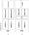
図10(A),(B)は、出力セレクタ方式と本実施形態に係る出力バッファ部とのレイアウトを比較して示す図である。
図10に示すように、スイッチ(SW)サイズは、スイッチが出力経路に接続されないためON抵抗を小さくする必要がなく、サイズを削減できる。
10A and 10B are diagrams showing a comparison between the layouts of the output selector method and the output buffer unit according to the present embodiment.
As shown in FIG. 10, the switch (SW) size can be reduced because the switch is not connected to the output path, so that the ON resistance need not be reduced.
また、出力段の第1および第2のOAMP212,222のサイズも、シリーズに接続されるスイッチ(SW)がないため、素子サイズが削減可能となる。 Also, the size of the first and second OAMPs 212 and 222 of the output stage can be reduced because there is no switch (SW) connected to the series.
また、図11(A),(B)は、出力セレクタ方式と本実施形態に係る出力バッファ部とのバイアス段のオフセットの見え方の差異であって、出力段起因によるオフセット電圧の影響を比較して示す図である。 11A and 11B show the difference in the bias stage offset appearance between the output selector method and the output buffer unit according to the present embodiment, and compare the influence of the offset voltage caused by the output stage. It is a figure shown.
出力段AMP起因のオフセット電圧が合った場合、出力セレクタ方式では、図11(A)に示すように、オフセット電圧がキャンセルされることはなく、輝度が理想からはずれる。
この出力セレクタ方式の場合、コモン電圧Vcomの中心電圧からの平均電圧はVa+(Δ1+Δ2)/2となり、オフセットがキャンセルされることはない。
When the offset voltage due to the output stage AMP matches, the output selector method does not cancel the offset voltage as shown in FIG.
In the case of this output selector method, the average voltage from the center voltage of the common voltage Vcom is Va + (Δ1 + Δ2) / 2, and the offset is not canceled.
これに対して、本実施形態の出力バッファ部によれば、図11(B)に示すように、極性反転によりオフセットが2フレームで打ち消しあうことができる。
この場合、コモン電圧Vcomの中心電圧からの平均電圧はオフセット値Δ1、Δ2の値にかかわらずΔaである。
On the other hand, according to the output buffer unit of the present embodiment, as shown in FIG. 11B, the offset can be canceled in two frames by polarity inversion.
In this case, the average voltage from the center voltage of the common voltage Vcom is Δa regardless of the offset values Δ1 and Δ2.
以上説明したように、本実施形態によれば、出力バッファ部200は、前段のDAC123の出力に対して接続された入力データを増幅し、正極性の信号電圧を生成する機能を有する正極性側OTA211と、出力バッファとしての機能を有し、チャネルCHm(たとえばm=1)に接続される第1の信号線112mに正極性または負極性の信号電圧を供給する第1のOAMP212と、前段のDAC123の出力に対して接続され入力データを増幅し、負正極性の信号電圧を生成する機能を有する負極性側OTA221と、出力バッファとしての機能を有し、チャネルCHm+1(たとえばCH2)に接続される第2の信号線112m+1に負極性または正極性の信号電圧を供給する第2のOAMP222と、正極性側OTA211の出力および負極性側OTA221の出力の各々と、第1のOAMP212の入力および第2のOAMP222の入力の各々との間、並びに、正極性側OTA211および負極性側OTA221の帰還入力段に第1のスイッチSW231〜第8のSW238を含むスイッチ群230と、を有することから、以下の効果を得ることができる。
出力経路にスイッチ(SW)をいれることなく、出力バッファ部の内部へ切り替えスイッチ(SW)を配置するため、スイッチ(SW)サイズの削減ができ、レイアウト面積を削減することが可能となる。
出力経路にスイッチ(SW)がないため、出力段のMOSサイズが削減でき、レイアウト面積を削減することが可能となる。
同様に、出力経路のスイッチ(SW)がないため、セトリングが改善され、特性の改善を図ることができる。
また、出力段の増幅器に起因のオフセット成分が、極性反転により光学的にキャンセルでき、特性改善を図れ、ひいては画質の向上を図ることができる。
As described above, according to the present embodiment, the output buffer unit 200 amplifies the input data connected to the output of the
Since the changeover switch (SW) is arranged inside the output buffer unit without putting the switch (SW) in the output path, the size of the switch (SW) can be reduced, and the layout area can be reduced.
Since there is no switch (SW) in the output path, the MOS size of the output stage can be reduced, and the layout area can be reduced.
Similarly, since there is no switch (SW) in the output path, settling is improved and characteristics can be improved.
In addition, the offset component caused by the amplifier at the output stage can be optically canceled by polarity inversion, so that the characteristics can be improved and the image quality can be improved.
なお、上記実施形態では、アクティブマトリクス型液晶表示装置に適用した場合を例に採って説明したが、これに限定されるものではなく、エレクトロルミネッセンス(EL)素子を各画素の電気光学素子として用いたEL表示装置などの他のアクティブマトリクス型表示装置にも同様に適用可能である。 In the above embodiment, the case where the present invention is applied to an active matrix liquid crystal display device has been described as an example. However, the present invention is not limited to this, and an electroluminescence (EL) element is used as an electro-optical element of each pixel. The present invention can be similarly applied to other active matrix display devices such as EL display devices.
またさらに、上記実施形態に係るアクティブマトリクス型液晶表示装置に代表されるアクティブマトリクス型表示装置は、図12〜図16に示す様々な電子機器、たとえば、デジタルカメラ、ノート型パーソナルコンピュータ、携帯電話等の携帯端末装置(モバイル機器)、デスクトップ型パーソナルコンピュータ、ビデオカメラなど、電子機器に入力された映像信号、若しくは、電子機器内で生成した映像信号を、画像若しくは映像として表示するあらゆる分野の電子機器の表示装置に適用することが可能である。
以下に、本実施形態が適用される電子機器の一例について説明する。
Furthermore, an active matrix type display device represented by the active matrix type liquid crystal display device according to the above embodiment includes various electronic devices such as a digital camera, a notebook type personal computer, a mobile phone, and the like shown in FIGS. Electronic devices in all fields that display video signals input to electronic devices or video signals generated in electronic devices as images or videos, such as mobile terminal devices (mobile devices), desktop personal computers, video cameras, etc. It is possible to apply to the display device.
Below, an example of the electronic device to which this embodiment is applied is demonstrated.
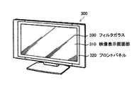
図12は、本実施形態が適用されるテレビジョンを示す斜視図である。
本適用例に係るテレビジョン300は、フロントパネル320やフィルターガラス330等から構成される映像表示画面部310を含み、その映像表示画面部310として本実施形態に係る表示装置を用いることにより作製される。
FIG. 12 is a perspective view showing a television to which the present embodiment is applied.
The
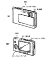
図13は、本実施形態が適用されるデジタルカメラを示す斜視図であり、図13(A)は表側から見た斜視図、図13(B)は裏側から見た斜視図である。
本適用例に係るデジタルカメラ300Aは、フラッシュ用の発光部311、表示部312、メニュースイッチ313、シャッターボタン314等を含み、その表示部312として本実施形態に係る表示装置を用いることにより作製される。
FIG. 13 is a perspective view showing a digital camera to which the present embodiment is applied. FIG. 13A is a perspective view seen from the front side, and FIG. 13B is a perspective view seen from the back side.
The
図14は、本実施形態が適用されるノート型パーソナルコンピュータを示す斜視図である。
本適用例に係るノート型パーソナルコンピュータ300Bは、本体321に、文字等を入力するとき操作されるキーボード322、画像を表示する表示部323等を含み、その表示部323として本実施形態に係る表示装置を用いることにより作製される。
FIG. 14 is a perspective view showing a notebook personal computer to which the present embodiment is applied.
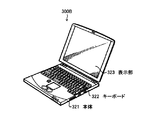
A notebook
図15は、本実施形態が適用されるビデオカメラを示す斜視図である。
本適用例に係るビデオカメラ300Cは、本体部331、前方を向いた側面に被写体撮影用のレンズ332、撮影時のスタート/ストップスイッチ333、表示部334等を含み、その表示部334として本実施形態に係る表示装置を用いることにより作製される。
FIG. 15 is a perspective view showing a video camera to which the present embodiment is applied.
A
図16は、本実施形態が適用される携帯端末装置、たとえば携帯電話機を示す図であり、図16(A)は開いた状態での正面図、図16(B)はその側面図、図16(C)は閉じた状態での正面図、図16(D)は左側面図、図16(E)は右側面図、図16(F)は上面図、図16(G)は下面図である。
本適用例に係る携帯電話機300Dは、上側筐体341、下側筐体342、連結部(ここではヒンジ部)343、ディスプレイ344、サブディスプレイ345、ピクチャーライト346、カメラ347等を含み、そのディスプレイ344やサブディスプレイ345として本実施形態に係る表示装置を用いることにより作製される。
FIG. 16 is a view showing a mobile terminal device to which the present embodiment is applied, for example, a mobile phone. FIG. 16 (A) is a front view in an opened state, FIG. 16 (B) is a side view thereof, FIG. 16C is a front view in a closed state, FIG. 16D is a left side view, FIG. 16E is a right side view, FIG. 16F is a top view, and FIG. is there.
A mobile phone 300D according to this application example includes an
100・・・液晶表示装置、110・・・有効表示部、120・・・信号線駆動回路(水平駆動回路、ソースドライバ:HDRV)、121・・・シフトレジスタ、122・・・データラッチ部、123・・・DAC(デジタル・アナログコンバータ)、124・・・出力バッファ部、130・・・ゲート線駆動回路(垂直駆動回路、ゲートドライバ)、140・・・データ処理回路(DATAPRC)、200・・・出力バッファ部、211・・・正極性側演算増幅器(OTA)、212・・・第1の共通出力増幅器(OAMP)、221・・・負極性側OTA、222・・・第2のOAMP、230・・・スイッチ群、SW231〜SW238・・・スイッチ。
DESCRIPTION OF
Claims (7)
信号線を駆動する入力データを増幅し、正極性の信号電圧および負極性の信号電圧を生成し、対をなす第1の信号線および第2の信号線に正極性の信号電圧および負極性の信号電圧を選択的に供給する出力バッファ部を有し、
上記出力バッファ部は、
入力データを増幅し、正極性の信号電圧を生成する正極性側演算増幅器と、
入力データを増幅し、負極性の信号電圧を生成する負極性側演算増幅器と、
上記第1の信号線に正極性または負極性の信号電圧を供給する第1の出力バッファと、
上記第2の信号線に負極性または正極性の信号電圧を供給する第2の出力バッファと、
上記正極性側演算増幅器の出力および上記負極性側演算増幅器の出力の各々と、上記第1の出力バッファの入力および上記第2の出力バッファの入力の各々との間、並びに、上記正極性側演算増幅器および上記負極性側演算増幅器の帰還入力段に配置されたスイッチ群と、を含み、
上記スイッチ群は、
第1のモード時は、
上記正極性側演算増幅器で生成された正極性の信号電圧を上記第1の出力バッファに入力し、当該第1の出力バッファの出力を上記正極性側演算増幅器に帰還させ、
上記負極性側演算増幅器で生成された負極性の信号電圧を上記第2の出力バッファに入力し、当該第2の出力バッファの出力を上記負極性側演算増幅器に帰還させ、
第2のモード時は、
上記正極性側演算増幅器で生成された正極性の信号電圧を上記第2の出力バッファに入力し、当該第2の出力バッファの出力を上記正極性側演算増幅器に帰還させ、
上記負極性側演算増幅器で生成された負極性の信号電圧を上記第1の出力バッファに入力し、当該第1の出力バッファの出力を上記負極性側演算増幅器に帰還させ、
上記第1の出力バッファの出力と上記第1の信号線との間、並びに上記第2の出力バッファの出力と上記第2の信号線との間には、スイッチが介在しない
信号線駆動回路。 A signal line driving circuit in which display cells driven in polarity inversion are arranged in a matrix and supplies a positive signal voltage or a negative signal voltage to a signal line connected to the display cell corresponding to the polarity inversion. There,
It amplifies the input data for driving a signal line, and generates a signal voltage of positive polarity and negative polarity of the signal voltage, the first signal line and second signal line pairs of the positive polarity signal voltage and the negative polarity An output buffer for selectively supplying a signal voltage;
The output buffer unit
A positive-side operational amplifier that amplifies input data and generates a positive signal voltage;
A negative-side operational amplifier that amplifies input data and generates a negative-polarity signal voltage;
A first output buffer for supplying a positive or negative signal voltage to the first signal line;
A second output buffer for supplying a negative or positive signal voltage to the second signal line;
Between each of the output of the positive polarity side operational amplifier and the output of the negative polarity side operational amplifier, the input of the first output buffer and the input of the second output buffer, and the positive polarity side An operational amplifier and a switch group disposed in the feedback input stage of the negative polarity side operational amplifier,
The above switches are
In the first mode,
The positive polarity signal voltage generated by the positive polarity side operational amplifier is input to the first output buffer, and the output of the first output buffer is fed back to the positive polarity side operational amplifier,
The negative signal voltage generated by the negative operational amplifier is input to the second output buffer, and the output of the second output buffer is fed back to the negative operational amplifier.
In the second mode,
A positive signal voltage generated by the positive operational amplifier is input to the second output buffer, and an output of the second output buffer is fed back to the positive operational amplifier;
A negative signal voltage generated by the negative polarity side operational amplifier is input to the first output buffer, and an output of the first output buffer is fed back to the negative polarity side operational amplifier;
A signal line driver circuit in which no switch is interposed between the output of the first output buffer and the first signal line and between the output of the second output buffer and the second signal line.
第1導電型トランジスタの差動対を有し、
上記負極性側演算増幅器は、
第2導電型トランジスタの差動対を有し、
上記第1および第2の出力バッファは、
AB級プシュプル動作機能を有する
請求項1記載の信号線駆動回路。 The positive polarity side operational amplifier is:
Having a differential pair of first conductivity type transistors;
The negative polarity side operational amplifier is
Having a differential pair of second conductivity type transistors;
The first and second output buffers are:
The signal line drive circuit according to claim 1, having a class AB push-pull operation function.
請求項2記載の信号線駆動回路。 The signal line drive circuit according to claim 2, wherein the first and second output buffers have two input terminals.
上記極性反転に対応して上記表示セルに接続される信号線に正極性の信号電圧または負極性の信号電圧を供給する信号線駆動回路と、を有し、
上記信号線駆動回路は、
信号線を駆動する入力データを増幅し、正極性の信号電圧および負極性の信号電圧を生成し、対をなす第1の信号線および第2の信号線に正極性の信号電圧および負極性の信号電圧を選択的に供給する出力バッファ部を含み、
上記出力バッファ部は、
入力データを増幅し、正極性の信号電圧を生成する正極性側演算増幅器と、
入力データを増幅し、負極性の信号電圧を生成する負極性側演算増幅器と、
上記第1の信号線に正極性または負極性の信号電圧を供給する第1の出力バッファと、
上記第2の信号線に負極性または正極性の信号電圧を供給する第2の出力バッファと、
上記正極性側演算増幅器の出力および上記負極性側演算増幅器の出力の各々と、上記第1の出力バッファの入力および上記第2の出力バッファの入力の各々との間、並びに、上記正極性側演算増幅器および上記負極性側演算増幅器の帰還入力段に配置されたスイッチ群と、を含み、
上記スイッチ群は、
第1のモード時は、
上記正極性側演算増幅器で生成された正極性の信号電圧を上記第1の出力バッファに入力し、当該第1の出力バッファの出力を上記正極性側演算増幅器に帰還させ、
上記負極性側演算増幅器で生成された負極性の信号電圧を上記第2の出力バッファに入力し、当該第2の出力バッファの出力を上記負極性側演算増幅器に帰還させ、
第2のモード時は、
上記正極性側演算増幅器で生成された正極性の信号電圧を上記第2の出力バッファに入力し、当該第2の出力バッファの出力を上記正極性側演算増幅器に帰還させ、
上記負極性側演算増幅器で生成された負極性の信号電圧を上記第1の出力バッファに入力し、当該第1の出力バッファの出力を上記負極性側演算増幅器に帰還させ、
上記第1の出力バッファの出力と上記第1の信号線との間、並びに上記第2の出力バッファの出力と上記第2の信号線との間には、スイッチが介在しない
表示装置。 A display unit in which display cells to be polarity-inverted are arranged in a matrix;
A signal line driving circuit that supplies a positive signal voltage or a negative signal voltage to a signal line connected to the display cell in response to the polarity inversion,
The signal line driving circuit is
It amplifies the input data for driving a signal line, and generates a signal voltage of positive polarity and negative polarity of the signal voltage, the first signal line and second signal line pairs of the positive polarity signal voltage and the negative polarity Including an output buffer for selectively supplying a signal voltage;
The output buffer unit
A positive-side operational amplifier that amplifies input data and generates a positive signal voltage;
A negative-side operational amplifier that amplifies input data and generates a negative-polarity signal voltage;
A first output buffer for supplying a positive or negative signal voltage to the first signal line;
A second output buffer for supplying a negative or positive signal voltage to the second signal line;
Between each of the output of the positive polarity side operational amplifier and the output of the negative polarity side operational amplifier, the input of the first output buffer and the input of the second output buffer, and the positive polarity side An operational amplifier and a switch group disposed in the feedback input stage of the negative polarity side operational amplifier,
The above switches are
In the first mode,
The positive polarity signal voltage generated by the positive polarity side operational amplifier is input to the first output buffer, and the output of the first output buffer is fed back to the positive polarity side operational amplifier,
The negative signal voltage generated by the negative operational amplifier is input to the second output buffer, and the output of the second output buffer is fed back to the negative operational amplifier.
In the second mode,
A positive signal voltage generated by the positive operational amplifier is input to the second output buffer, and an output of the second output buffer is fed back to the positive operational amplifier;
A negative signal voltage generated by the negative polarity side operational amplifier is input to the first output buffer, and an output of the first output buffer is fed back to the negative polarity side operational amplifier;
A display device in which no switch is interposed between the output of the first output buffer and the first signal line, and between the output of the second output buffer and the second signal line.
第1導電型トランジスタの差動対を有し、
上記負極性側演算増幅器は、
第2導電型トランジスタの差動対を有し、
上記第1および第2の出力バッファは、
AB級プシュプル動作機能を有する
請求項4記載の表示装置。 The positive polarity side operational amplifier is:
Having a differential pair of first conductivity type transistors;
The negative polarity side operational amplifier is
Having a differential pair of second conductivity type transistors;
The first and second output buffers are:
The display device according to claim 4 , having a class AB push-pull operation function.
請求項5記載の表示装置。 The display device according to claim 5, wherein the first and second output buffers have two input terminals.
上記表示装置は、
極性反転駆動される表示セルがマトリクス状に配置される表示部と、
上記極性反転に対応して上記表示セルに接続される信号線に正極性の信号電圧または負極性の信号電圧を供給する信号線駆動回路と、を有し、
上記信号線駆動回路は、
信号線を駆動する入力データを増幅し、正極性の信号電圧および負極性の信号電圧を生成し、対をなす第1の信号線および第2の信号線に正極性の信号電圧および負極性の信号電圧を選択的に供給する出力バッファ部を含み、
上記出力バッファ部は、
入力データを増幅し、正極性の信号電圧を生成する正極性側演算増幅器と、
入力データを増幅し、負極性の信号電圧を生成する負極性側演算増幅器と、
上記第1の信号線に正極性または負極性の信号電圧を供給する第1の出力バッファと、
上記第2の信号線に負極性または正極性の信号電圧を供給する第2の出力バッファと、
上記正極性側演算増幅器の出力および上記負極性側演算増幅器の出力の各々と、上記第1の出力バッファの入力および上記第2の出力バッファの入力の各々との間、並びに、上記正極性側演算増幅器および上記負極性側演算増幅器の帰還入力段に配置されたスイッチ群と、を含み、
上記スイッチ群は、
第1のモード時は、
上記正極性側演算増幅器で生成された正極性の信号電圧を上記第1の出力バッファに入力し、当該第1の出力バッファの出力を上記正極性側演算増幅器に帰還させ、
上記負極性側演算増幅器で生成された負極性の信号電圧を上記第2の出力バッファに入力し、当該第2の出力バッファの出力を上記負極性側演算増幅器に帰還させ、
第2のモード時は、
上記正極性側演算増幅器で生成された正極性の信号電圧を上記第2の出力バッファに入力し、当該第2の出力バッファの出力を上記正極性側演算増幅器に帰還させ、
上記負極性側演算増幅器で生成された負極性の信号電圧を上記第1の出力バッファに入力し、当該第1の出力バッファの出力を上記負極性側演算増幅器に帰還させ、
上記第1の出力バッファの出力と上記第1の信号線との間、並びに上記第2の出力バッファの出力と上記第2の信号線との間には、スイッチが介在しない
電子機器。 An electronic device having a display device,
The display device
A display unit in which display cells to be polarity-inverted are arranged in a matrix;
A signal line driving circuit that supplies a positive signal voltage or a negative signal voltage to a signal line connected to the display cell in response to the polarity inversion,
The signal line driving circuit is
It amplifies the input data for driving a signal line, and generates a signal voltage of positive polarity and negative polarity of the signal voltage, the first signal line and second signal line pairs of the positive polarity signal voltage and the negative polarity Including an output buffer for selectively supplying a signal voltage;
The output buffer unit
A positive-side operational amplifier that amplifies input data and generates a positive signal voltage;
A negative-side operational amplifier that amplifies input data and generates a negative-polarity signal voltage;
A first output buffer for supplying a positive or negative signal voltage to the first signal line;
A second output buffer for supplying a negative or positive signal voltage to the second signal line;
Between each of the output of the positive polarity side operational amplifier and the output of the negative polarity side operational amplifier, the input of the first output buffer and the input of the second output buffer, and the positive polarity side An operational amplifier and a switch group disposed in the feedback input stage of the negative polarity side operational amplifier,
The above switches are
In the first mode,
The positive polarity signal voltage generated by the positive polarity side operational amplifier is input to the first output buffer, and the output of the first output buffer is fed back to the positive polarity side operational amplifier,
The negative signal voltage generated by the negative operational amplifier is input to the second output buffer, and the output of the second output buffer is fed back to the negative operational amplifier.
In the second mode,
A positive signal voltage generated by the positive operational amplifier is input to the second output buffer, and an output of the second output buffer is fed back to the positive operational amplifier;
A negative signal voltage generated by the negative polarity side operational amplifier is input to the first output buffer, and an output of the first output buffer is fed back to the negative polarity side operational amplifier;
An electronic device in which no switch is interposed between the output of the first output buffer and the first signal line, and between the output of the second output buffer and the second signal line.
Priority Applications (6)
| Application Number | Priority Date | Filing Date | Title |
|---|---|---|---|
| JP2007338996A JP4466735B2 (en) | 2007-12-28 | 2007-12-28 | SIGNAL LINE DRIVE CIRCUIT, DISPLAY DEVICE, AND ELECTRONIC DEVICE |
| US12/271,622 US9275596B2 (en) | 2007-12-28 | 2008-11-14 | Signal-line driving circuit, display device and electronic equipments |
| KR1020080117644A KR101531325B1 (en) | 2007-12-28 | 2008-11-25 | Signal line drive circuits and display devices and electronic devices |
| TW097148955A TWI405173B (en) | 2007-12-28 | 2008-12-16 | Signal-line driving circuit, display device and electronic equipments |
| EP08022293.8A EP2075788B1 (en) | 2007-12-28 | 2008-12-22 | Signal-line driving circuit, display device and electronic equipments |
| CN2008101873141A CN101504816B (en) | 2007-12-28 | 2008-12-26 | Signal-line driving circuit, display device and electronic equipments |
Applications Claiming Priority (1)
| Application Number | Priority Date | Filing Date | Title |
|---|---|---|---|
| JP2007338996A JP4466735B2 (en) | 2007-12-28 | 2007-12-28 | SIGNAL LINE DRIVE CIRCUIT, DISPLAY DEVICE, AND ELECTRONIC DEVICE |
Publications (2)
| Publication Number | Publication Date |
|---|---|
| JP2009162789A JP2009162789A (en) | 2009-07-23 |
| JP4466735B2 true JP4466735B2 (en) | 2010-05-26 |
Family
ID=40377395
Family Applications (1)
| Application Number | Title | Priority Date | Filing Date |
|---|---|---|---|
| JP2007338996A Expired - Fee Related JP4466735B2 (en) | 2007-12-28 | 2007-12-28 | SIGNAL LINE DRIVE CIRCUIT, DISPLAY DEVICE, AND ELECTRONIC DEVICE |
Country Status (6)
| Country | Link |
|---|---|
| US (1) | US9275596B2 (en) |
| EP (1) | EP2075788B1 (en) |
| JP (1) | JP4466735B2 (en) |
| KR (1) | KR101531325B1 (en) |
| CN (1) | CN101504816B (en) |
| TW (1) | TWI405173B (en) |
Families Citing this family (29)
| Publication number | Priority date | Publication date | Assignee | Title |
|---|---|---|---|---|
| JP5236434B2 (en) * | 2008-11-21 | 2013-07-17 | ラピスセミコンダクタ株式会社 | Display panel drive voltage output circuit |
| KR101581723B1 (en) * | 2008-12-26 | 2015-12-31 | 주식회사 동부하이텍 | Amp output protective circuit for lcd panel source driver and method thereof |
| JP5172748B2 (en) * | 2009-03-11 | 2013-03-27 | ルネサスエレクトロニクス株式会社 | Display panel driver and display device using the same |
| CN102044204B (en) * | 2009-10-13 | 2013-01-02 | 瑞鼎科技股份有限公司 | Driving circuit, electronic display device using same and driving method thereof |
| US8830155B2 (en) * | 2009-10-30 | 2014-09-09 | Au Optronics Corporation | Method and source driver for driving liquid crystal display |
| CN102081896B (en) * | 2009-11-26 | 2013-02-13 | 奇景光电股份有限公司 | Source driver, display device and driving method of display panel |
| KR101579839B1 (en) * | 2009-12-23 | 2015-12-23 | 삼성전자주식회사 | Output Buffer Having High Slew Rate, Output Buffer Control Method, and Display Driver Having It |
| JP5374356B2 (en) * | 2009-12-28 | 2013-12-25 | ラピスセミコンダクタ株式会社 | Driving circuit and display device |
| CN102195635A (en) * | 2010-03-04 | 2011-09-21 | 联咏科技股份有限公司 | Output buffer circuit capable of improving stability |
| TW201241815A (en) * | 2011-04-01 | 2012-10-16 | Fitipower Integrated Tech Inc | Source driver of LCD panel |
| CN102768824A (en) * | 2011-05-05 | 2012-11-07 | 天钰科技股份有限公司 | Source Drivers for LCD Panels |
| CN103325346A (en) * | 2012-03-22 | 2013-09-25 | 联咏科技股份有限公司 | Driving control method and correlative source electrode driver |
| CN102721453B (en) * | 2012-07-13 | 2014-09-03 | 广州市浩云安防科技股份有限公司 | Gun-bullet separation induction device |
| SG10201609410PA (en) * | 2015-11-30 | 2017-06-29 | Semiconductor Energy Lab | Semiconductor device, display panel, and electronic device |
| WO2018150290A1 (en) * | 2017-02-16 | 2018-08-23 | Semiconductor Energy Laboratory Co., Ltd. | Semiconductor device, display panel, display device, input/output device, and data processing device |
| TWI630791B (en) * | 2017-09-22 | 2018-07-21 | 奇景光電股份有限公司 | Channel operational amplifier and method for a channel operational amplifier |
| CN107610633B (en) * | 2017-09-28 | 2020-12-04 | 惠科股份有限公司 | Driving device and driving method of display panel |
| KR102755209B1 (en) * | 2018-06-15 | 2025-01-17 | 엘지디스플레이 주식회사 | Touch display device, data driving circuit and method for driving controller |
| US10802636B2 (en) * | 2018-06-15 | 2020-10-13 | Lg Display Co., Ltd. | Touch display device, data driver circuit, and method of driving controller |
| CN111312182B (en) * | 2018-12-12 | 2022-03-11 | 咸阳彩虹光电科技有限公司 | Source electrode driving circuit, liquid crystal display and source electrode driving method |
| KR102611010B1 (en) * | 2018-12-24 | 2023-12-07 | 주식회사 엘엑스세미콘 | Source driving circuit |
| TWI674757B (en) * | 2019-02-13 | 2019-10-11 | 奕力科技股份有限公司 | Buffer circuit |
| CN109903730B (en) * | 2019-02-13 | 2021-04-06 | 奕力科技(开曼)股份有限公司 | Buffer circuit |
| CN110728960A (en) * | 2019-10-21 | 2020-01-24 | 湖南国科微电子股份有限公司 | LCD drive circuit and display device |
| US11196397B2 (en) * | 2019-12-31 | 2021-12-07 | Novatek Microelectronics Corp. | Current integrator for OLED panel |
| US11393375B2 (en) * | 2020-09-30 | 2022-07-19 | Himax Technologies Limited | Source driver and polarity inversion control circuit |
| JP7544624B2 (en) * | 2021-02-19 | 2024-09-03 | ラピステクノロジー株式会社 | OUTPUT CIRCUIT, DISPLAY DRIVER AND DISPLAY DEVICE |
| CN113889043B (en) * | 2021-09-30 | 2023-04-14 | 晟合微电子(肇庆)有限公司 | Display driving circuit and display panel |
| CN113903316B (en) * | 2021-10-19 | 2023-08-01 | 上海新相微电子股份有限公司 | TFT LCD driving chip is to display screen source parasitic capacitance charge recovery circuit |
Family Cites Families (22)
| Publication number | Priority date | Publication date | Assignee | Title |
|---|---|---|---|---|
| JPH10153986A (en) | 1996-09-25 | 1998-06-09 | Toshiba Corp | Display device |
| JP3369875B2 (en) | 1996-11-12 | 2003-01-20 | 株式会社東芝 | LCD drive circuit |
| US6480178B1 (en) * | 1997-08-05 | 2002-11-12 | Kabushiki Kaisha Toshiba | Amplifier circuit and liquid-crystal display unit using the same |
| JP3550016B2 (en) | 1998-03-03 | 2004-08-04 | 株式会社 日立ディスプレイズ | Method of driving liquid crystal display device and method of outputting video signal voltage |
| US6304241B1 (en) | 1998-06-03 | 2001-10-16 | Fujitsu Limited | Driver for a liquid-crystal display panel |
| JP3481166B2 (en) | 1999-07-16 | 2003-12-22 | 松下電器産業株式会社 | Liquid crystal drive |
| JP4806481B2 (en) | 1999-08-19 | 2011-11-02 | 富士通セミコンダクター株式会社 | LCD panel drive circuit |
| JP3506235B2 (en) | 2000-08-18 | 2004-03-15 | シャープ株式会社 | Driving device and driving method for liquid crystal display device |
| JP4744686B2 (en) | 2000-12-06 | 2011-08-10 | ルネサスエレクトロニクス株式会社 | Operational amplifier |
| JP4437378B2 (en) * | 2001-06-07 | 2010-03-24 | 株式会社日立製作所 | Liquid crystal drive device |
| JP2003115729A (en) | 2001-10-02 | 2003-04-18 | Seiko Epson Corp | AB class amplifier |
| JP3908013B2 (en) * | 2001-11-19 | 2007-04-25 | Necエレクトロニクス株式会社 | Display control circuit and display device |
| JP3991306B2 (en) | 2001-11-20 | 2007-10-17 | ソニー株式会社 | Amplifier circuit |
| US6970152B1 (en) * | 2002-11-05 | 2005-11-29 | National Semiconductor Corporation | Stacked amplifier arrangement for graphics displays |
| KR100517734B1 (en) * | 2003-12-12 | 2005-09-29 | 삼성전자주식회사 | Apparatus and Method for Converting Digital Data to Gamma Corrected Analog Signal, Source Driver Integrated Circuits and Flat Panel Display using the same |
| JP4502207B2 (en) | 2005-12-28 | 2010-07-14 | ルネサスエレクトロニクス株式会社 | Differential amplifier, data driver and display device |
| TWI342000B (en) | 2006-01-03 | 2011-05-11 | Sunplus Technology Co Ltd | Driving circuit for tft liquid crystal display |
| KR100790977B1 (en) * | 2006-01-13 | 2008-01-03 | 삼성전자주식회사 | Output buffer with improved output deviation and source driver for flat panel display |
| JP4637077B2 (en) * | 2006-10-17 | 2011-02-23 | パナソニック株式会社 | Drive voltage output circuit, display device |
| JP2008102345A (en) | 2006-10-19 | 2008-05-01 | Nec Electronics Corp | Semiconductor integrated circuit device |
| JP4861791B2 (en) * | 2006-10-27 | 2012-01-25 | ルネサスエレクトロニクス株式会社 | Operational amplifier and display device |
| KR100883030B1 (en) * | 2007-02-28 | 2009-02-09 | 매그나칩 반도체 유한회사 | Driving circuit and method of flat panel display |
-
2007
- 2007-12-28 JP JP2007338996A patent/JP4466735B2/en not_active Expired - Fee Related
-
2008
- 2008-11-14 US US12/271,622 patent/US9275596B2/en active Active
- 2008-11-25 KR KR1020080117644A patent/KR101531325B1/en not_active Expired - Fee Related
- 2008-12-16 TW TW097148955A patent/TWI405173B/en not_active IP Right Cessation
- 2008-12-22 EP EP08022293.8A patent/EP2075788B1/en not_active Not-in-force
- 2008-12-26 CN CN2008101873141A patent/CN101504816B/en not_active Expired - Fee Related
Also Published As
| Publication number | Publication date |
|---|---|
| TW200947408A (en) | 2009-11-16 |
| EP2075788A3 (en) | 2010-08-25 |
| EP2075788B1 (en) | 2013-06-19 |
| TWI405173B (en) | 2013-08-11 |
| US9275596B2 (en) | 2016-03-01 |
| EP2075788A2 (en) | 2009-07-01 |
| KR101531325B1 (en) | 2015-06-24 |
| CN101504816B (en) | 2011-07-06 |
| CN101504816A (en) | 2009-08-12 |
| JP2009162789A (en) | 2009-07-23 |
| US20090167667A1 (en) | 2009-07-02 |
| KR20090072952A (en) | 2009-07-02 |
Similar Documents
| Publication | Publication Date | Title |
|---|---|---|
| JP4466735B2 (en) | SIGNAL LINE DRIVE CIRCUIT, DISPLAY DEVICE, AND ELECTRONIC DEVICE | |
| CN101930706B (en) | Signal-line driving circuit, display apparatus and electronic apparatus | |
| JP3605829B2 (en) | Electro-optical device driving circuit, electro-optical device driving method, electro-optical device, and electronic apparatus using the same | |
| US7071669B2 (en) | Reference voltage generation circuit, display driver circuit, display device, and method of generating reference voltage | |
| US7079127B2 (en) | Reference voltage generation circuit, display driver circuit, display device, and method of generating reference voltage | |
| US7586504B2 (en) | Amplifier circuit, driving circuit of display apparatus, portable telephone and portable electronic apparatus | |
| JP4449189B2 (en) | Image display device and driving method thereof | |
| US7443239B2 (en) | Differential amplifier, data driver and display device | |
| US7907136B2 (en) | Voltage generation circuit | |
| US7495512B2 (en) | Differential amplifier, data driver and display device | |
| US20090040165A1 (en) | Amplifying circuit and display unit | |
| US20090096816A1 (en) | Data driver, integrated circuit device, and electronic instrument | |
| US20130342520A1 (en) | Digital-to-analog-conversion circuit and data driver for display device | |
| US20100013686A1 (en) | Sample and hold circuit and digital-to-analog converter circuit | |
| KR100607772B1 (en) | Driver including voltage-follower-type operational amplifier with high driving power and display apparatus using the same | |
| JP5017871B2 (en) | Differential amplifier and digital-analog converter | |
| US8237649B2 (en) | Liquid crystal driving device | |
| KR100930154B1 (en) | Timing Generation Circuits, Display Units, and Portable Terminals | |
| JP2013218021A (en) | Data driver device and display device | |
| US8823687B2 (en) | Signal line drive circuit, display device and electronic apparatus | |
| JP5086010B2 (en) | LCD panel drive circuit | |
| JP2009168842A (en) | Reference voltage generation circuit, driver, electro-optical device, and electronic apparatus | |
| JP4962402B2 (en) | Electro-optical device drive circuit, electro-optical device, and electronic apparatus | |
| JP2011013491A (en) | Output circuit, signal line driving circuit, display device and electronic apparatus | |
| JP2009169387A (en) | Integrated circuit device, electro-optical device and electronic apparatus |
Legal Events
| Date | Code | Title | Description |
|---|---|---|---|
| A977 | Report on retrieval |
Free format text: JAPANESE INTERMEDIATE CODE: A971007 Effective date: 20091110 |
|
| A131 | Notification of reasons for refusal |
Free format text: JAPANESE INTERMEDIATE CODE: A131 Effective date: 20091117 |
|
| A521 | Request for written amendment filed |
Free format text: JAPANESE INTERMEDIATE CODE: A523 Effective date: 20100112 |
|
| TRDD | Decision of grant or rejection written | ||
| A01 | Written decision to grant a patent or to grant a registration (utility model) |
Free format text: JAPANESE INTERMEDIATE CODE: A01 Effective date: 20100202 |
|
| A01 | Written decision to grant a patent or to grant a registration (utility model) |
Free format text: JAPANESE INTERMEDIATE CODE: A01 |
|
| A61 | First payment of annual fees (during grant procedure) |
Free format text: JAPANESE INTERMEDIATE CODE: A61 Effective date: 20100215 |
|
| R151 | Written notification of patent or utility model registration |
Ref document number: 4466735 Country of ref document: JP Free format text: JAPANESE INTERMEDIATE CODE: R151 |
|
| FPAY | Renewal fee payment (event date is renewal date of database) |
Free format text: PAYMENT UNTIL: 20130305 Year of fee payment: 3 |
|
| FPAY | Renewal fee payment (event date is renewal date of database) |
Free format text: PAYMENT UNTIL: 20130305 Year of fee payment: 3 |
|
| FPAY | Renewal fee payment (event date is renewal date of database) |
Free format text: PAYMENT UNTIL: 20140305 Year of fee payment: 4 |
|
| R250 | Receipt of annual fees |
Free format text: JAPANESE INTERMEDIATE CODE: R250 |
|
| R250 | Receipt of annual fees |
Free format text: JAPANESE INTERMEDIATE CODE: R250 |
|
| R250 | Receipt of annual fees |
Free format text: JAPANESE INTERMEDIATE CODE: R250 |
|
| R250 | Receipt of annual fees |
Free format text: JAPANESE INTERMEDIATE CODE: R250 |
|
| R250 | Receipt of annual fees |
Free format text: JAPANESE INTERMEDIATE CODE: R250 |
|
| R250 | Receipt of annual fees |
Free format text: JAPANESE INTERMEDIATE CODE: R250 |
|
| R250 | Receipt of annual fees |
Free format text: JAPANESE INTERMEDIATE CODE: R250 |
|
| R250 | Receipt of annual fees |
Free format text: JAPANESE INTERMEDIATE CODE: R250 |
|
| R250 | Receipt of annual fees |
Free format text: JAPANESE INTERMEDIATE CODE: R250 |
|
| R250 | Receipt of annual fees |
Free format text: JAPANESE INTERMEDIATE CODE: R250 |
|
| LAPS | Cancellation because of no payment of annual fees |