US8026526B2 - Optoelectronic semiconductor component - Google Patents
Optoelectronic semiconductor component Download PDFInfo
- Publication number
- US8026526B2 US8026526B2 US12/478,517 US47851709A US8026526B2 US 8026526 B2 US8026526 B2 US 8026526B2 US 47851709 A US47851709 A US 47851709A US 8026526 B2 US8026526 B2 US 8026526B2
- Authority
- US
- United States
- Prior art keywords
- covering layer
- encapsulation
- basic body
- terminates
- component according
- Prior art date
- Legal status (The legal status is an assumption and is not a legal conclusion. Google has not performed a legal analysis and makes no representation as to the accuracy of the status listed.)
- Expired - Fee Related, expires
Links
Images


Classifications
-
- H—ELECTRICITY
- H10—SEMICONDUCTOR DEVICES; ELECTRIC SOLID-STATE DEVICES NOT OTHERWISE PROVIDED FOR
- H10H—INORGANIC LIGHT-EMITTING SEMICONDUCTOR DEVICES HAVING POTENTIAL BARRIERS
- H10H20/00—Individual inorganic light-emitting semiconductor devices having potential barriers, e.g. light-emitting diodes [LED]
- H10H20/80—Constructional details
- H10H20/84—Coatings, e.g. passivation layers or antireflective coatings
-
- H—ELECTRICITY
- H10—SEMICONDUCTOR DEVICES; ELECTRIC SOLID-STATE DEVICES NOT OTHERWISE PROVIDED FOR
- H10H—INORGANIC LIGHT-EMITTING SEMICONDUCTOR DEVICES HAVING POTENTIAL BARRIERS
- H10H20/00—Individual inorganic light-emitting semiconductor devices having potential barriers, e.g. light-emitting diodes [LED]
- H10H20/80—Constructional details
- H10H20/85—Packages
- H10H20/852—Encapsulations
- H10H20/854—Encapsulations characterised by their material, e.g. epoxy or silicone resins
-
- H—ELECTRICITY
- H10—SEMICONDUCTOR DEVICES; ELECTRIC SOLID-STATE DEVICES NOT OTHERWISE PROVIDED FOR
- H10W—GENERIC PACKAGES, INTERCONNECTIONS, CONNECTORS OR OTHER CONSTRUCTIONAL DETAILS OF DEVICES COVERED BY CLASS H10
- H10W74/00—Encapsulations, e.g. protective coatings
-
- H—ELECTRICITY
- H10—SEMICONDUCTOR DEVICES; ELECTRIC SOLID-STATE DEVICES NOT OTHERWISE PROVIDED FOR
- H10W—GENERIC PACKAGES, INTERCONNECTIONS, CONNECTORS OR OTHER CONSTRUCTIONAL DETAILS OF DEVICES COVERED BY CLASS H10
- H10W90/00—Package configurations
- H10W90/701—Package configurations characterised by the relative positions of pads or connectors relative to package parts
- H10W90/751—Package configurations characterised by the relative positions of pads or connectors relative to package parts of bond wires
- H10W90/756—Package configurations characterised by the relative positions of pads or connectors relative to package parts of bond wires between a chip and a stacked lead frame, conducting package substrate or heat sink
Definitions
- the invention relates to an optoelectronic semiconductor component comprising a basic body, at least one semiconductor chip arranged thereon, and an encapsulation embedding the at least one semiconductor chip and composed of a radiation-transmissive material with scattering particles.
- Optoelectronic semiconductor components are used, for example, in an area of display technology where a homogeneously illuminated and high-contrast image is important.
- a production method for conventional optoelectronic semiconductor components of the type mentioned involves firstly injection-molding a suitable plastic material around a prefabricated leadframe, the material forming a basic body for the housing of the device.
- the basic body has a cutout at the top side, connections of the leadframe being led into the cutout from two opposite sides.
- the semiconductor chip for example, an LED chip or a laser diode, is adhesively bonded and electrically contact-connected.
- a generally radiation-transmissive potting compound is then filled into the cutout and embeds the semiconductor body.
- the emission area is diffusely reflective.
- the contrast and the homogeneity of the image can be optimized further by the use of screen devices and/or diffuser plates disposed upstream of the optoelectronic semiconductor components. However, these devices also lead to a loss of light, such that the light emitted by the semiconductor chip must have a higher brightness.
- the invention specifies an optoelectronic semiconductor component, such that the light emitted by the semiconductor chip appears as a homogeneous luminous area and the semiconductor component enables a high-contrast image.
- an optoelectronic semiconductor component of the type mentioned in the introduction can be characterized in that a radiation-transmissive covering layer with an absorber is applied to the encapsulation.
- the optoelectronic semiconductor components according to the invention generate a homogeneously illuminated and high-contrast image on a video display, wherein the individual pixels appear homogeneously illuminated over the entire pixel area available to them, that is to say not as a small spot generated by the semiconductor chip.
- the edge regions or dimmed-down or switched-off regions of the image also appear black.
- a scattering particle density in the encapsulation has no influence on the absorption effect of the covering layer.
- the advantage is that the proportion of absorber in the covering layer, as the scattering particle density increases, does not have to be increased in order to obtain the same contrast. The absorption loss of the emitted light is therefore kept low.
- a further advantage is that in the case of an increased contrast, the brightness of the emitted light remains the same. That is to say that the requirements made of the brightness of the optoelectronic semiconductor component in the case of increased contrast are therefore reduced.
- contrast-enhancing elements disposed upstream of the semiconductor components can be obviated, for example a frame for screening against incident ambient light.
- the basic body is produced from a material which is at least partly absorbent for a radiation emitted by the semiconductor chip.
- the basic body is produced, for example, from a dark or black plastic. This results in a good contrast between the emission area of the component and the rest of the device area.
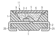
- FIG. 1 shows a schematic cross-sectional illustration of a first exemplary embodiment
- FIGS. 1A and 1B show other embodiments of the invention
- FIG. 2 shows a schematic cross-sectional illustration of a second exemplary embodiment
- FIG. 3 shows a schematic cross-sectional illustration of a third exemplary embodiment.
- FIGS. 1 to 3 show exemplary embodiments of an optoelectronic semiconductor component using surface mounting technology (SMT), wherein identical parts of the semiconductor component are identified by the same reference symbols in the figures.
- SMT surface mounting technology
- FIG. 1 shows a schematic cross-sectional view of an optoelectronic semiconductor component in accordance with a first exemplary embodiment of the present invention.
- the basic body 1 for the semiconductor component is formed by injection-molding a suitable plastic material around a leadframe 2 to form a housing.
- the basic body 1 has a central cutout, in which a semiconductor chip 3 such as, for example, an optoelectronic transmitter or receiver is arranged and is electrically conductively connected to the electrical connections 2 A, 2 B of the leadframe 2 by means of bonding wire technology 4 .
- An inner area 10 of the cutout of the basic body 1 is embodied in oblique fashion and produced from a black plastic. This results in a good contrast between an emission area 11 of the component and the rest of the device area of the basic body 1 .
- a plastic material preferably a thermoplastic or thermosetting plastic, is used for the basic body 1 .
- the semiconductor chip 3 is embedded in a radiation-transmissive encapsulation 6 , which is produced from a potting compound with scattering particles.
- the filling level of the encapsulation 6 terminates below the surface of the basic body 1 .
- other filling levels of the encapsulation 6 in the cutout of the basic body 1 can also be chosen, of course, as necessary. Two of such exemplary embodiments are shown in FIGS. 1A and 1B .
- a covering layer 5 with absorber which is a radiation-transmissive potting compound with absorber, is applied over the radiation-transmissive encapsulation 6 with scattering particles.
- the filling level of the covering layer 5 terminates with the surface of the basic body 1 .
- the absorber in the covering layer 5 absorbs externally incident extraneous light and thus prevents a reduction of a contrast due to reflection of the extraneous light at the emission area 11 or the chip surface. It is also possible to adhesively bond the covering layer 5 as lamina onto the encapsulation 6 .
- an epoxy resin or silicone is used as material for the potting compound of the encapsulation 6 and the covering layer 5 .
- the scattering particles in the encapsulation 6 are an aluminum oxide, for example.
- Carbon black, for example, is used as an absorber in the covering layer 5 .
- FIG. 1A shows an exemplary embodiment wherein the filling level of the encapsulation 6 in the cutout of the basic body 1 terminates with a step 8 in the inner area 10 .
- the filling level of the covering layer 5 applied to the encapsulation 6 terminates with the surface of the basic body 1 .
- the horizontal extent of the covering layer 5 is greater than the horizontal area of the encapsulation 6 that terminates at the step.
- FIG. 1B shows an exemplary embodiment wherein the filling level of the encapsulation 6 in the cutout of the basic body 1 terminates with a wave 9 in the inner area 10 .
- the filling level of the covering layer 5 applied to the encapsulation 6 terminates with the surface of the basic body 1 .
- the horizontal extent of the covering layer is greater than the horizontal area of the encapsulation 6 that terminates at the wave 9 .
- the filling level begins in an edge region of the covering layer 5 below the encapsulation 6 .
- FIG. 2 shows in a second exemplary embodiment a schematic cross-sectional illustration of an optoelectronic semiconductor component whose basic body 1 is formed by a substrate 7 .
- the semiconductor chip 3 is arranged on the substrate 7 and embedded in a two-layered body, namely the encapsulation 6 with scattering particles and, applied thereto, the covering layer 5 with absorber.
- the two-layered body is cast or injection-molded onto the substrate 7 , the covering layer 5 being cast or injection-molded onto the encapsulation 6 .
- the encapsulation 6 and the covering layer 5 are produced from epoxy resin, silicone or silicone-epoxide hybrid.
- the substrate 7 is produced from ceramic or epoxy resin with glass fiber fabric, also known by the abbreviation FR4.
- the scattering particles in the encapsulation 6 are an aluminum oxide, for example. Carbon black, for example, is used as absorber in the covering layer 5 .
- the covering layer 5 It is possible to adhesively bond the covering layer 5 over the encapsulations 6 of a plurality of semiconductor components and separate them from one another together with the semiconductor components. It is also possible to print the covering layer 5 onto the encapsulations 6 of a plurality of semiconductor components. However, the encapsulations 6 must then form a planar area.
- FIG. 3 shows in a third exemplary embodiment a schematic cross-sectional illustration of an optoelectronic semiconductor component whose basic body 1 is also formed by the substrate 7 .
- the semiconductor chip 3 is arranged on the substrate 7 and the semiconductor chip 3 is embedded in the two-layered body, namely the encapsulation 6 with scattering particles and, applied thereto, the covering layer 5 with absorber.
- the covering layer 5 is cast or injection-molded onto the encapsulation 6 .
- the covering layer 5 with absorber encapsulates the encapsulation 6 with scattering particles, wherein the filling level of the covering layer 5 reaches as far as the substrate 7 in this exemplary embodiment.
- Extraneous light incident into the semiconductor component is screened particularly effectively, wherein the brightness of the light emitted by the semiconductor chip does not have to be increased.
Landscapes
- Led Device Packages (AREA)
Applications Claiming Priority (4)
| Application Number | Priority Date | Filing Date | Title |
|---|---|---|---|
| DE102006059994A DE102006059994A1 (de) | 2006-12-19 | 2006-12-19 | Optoelektronisches Halbleiterbauelement |
| DE102006059994 | 2006-12-19 | ||
| DE102006059994.2 | 2006-12-19 | ||
| PCT/DE2007/002091 WO2008074286A1 (de) | 2006-12-19 | 2007-11-16 | Optoelektronisches halbleiterbauelement |
Related Parent Applications (1)
| Application Number | Title | Priority Date | Filing Date |
|---|---|---|---|
| PCT/DE2007/002091 Continuation WO2008074286A1 (de) | 2006-12-19 | 2007-11-16 | Optoelektronisches halbleiterbauelement |
Publications (2)
| Publication Number | Publication Date |
|---|---|
| US20090267107A1 US20090267107A1 (en) | 2009-10-29 |
| US8026526B2 true US8026526B2 (en) | 2011-09-27 |
Family
ID=39185899
Family Applications (1)
| Application Number | Title | Priority Date | Filing Date |
|---|---|---|---|
| US12/478,517 Expired - Fee Related US8026526B2 (en) | 2006-12-19 | 2009-06-04 | Optoelectronic semiconductor component |
Country Status (7)
| Country | Link |
|---|---|
| US (1) | US8026526B2 (de) |
| EP (1) | EP2054949B1 (de) |
| KR (1) | KR20090096616A (de) |
| CN (1) | CN101548396B (de) |
| DE (1) | DE102006059994A1 (de) |
| TW (1) | TWI389266B (de) |
| WO (1) | WO2008074286A1 (de) |
Cited By (8)
| Publication number | Priority date | Publication date | Assignee | Title |
|---|---|---|---|---|
| US20090261365A1 (en) * | 2005-09-30 | 2009-10-22 | Osram Opto Semiconductors Gmbh | Optoelectronic Componet Which Emits Electromagnetic Radiation, and Method for Production of an Optoelectronic Component |
| US20100230694A1 (en) * | 2007-03-30 | 2010-09-16 | Osram Opto Semiconductors Gmbh | Optoelectronical Component Emitting Electromagnetic Radiation and Method for Producing an Optoelectronical Component |
| US20110002587A1 (en) * | 2007-01-11 | 2011-01-06 | Georg Bogner | Housing for an Optoelectronic Component and Arrangement of an Optoelectronic Component in a Housing |
| US20110199788A1 (en) * | 2010-01-18 | 2011-08-18 | Park Joo Hyang | Lighting unit and display device having the same |
| US20130168705A1 (en) * | 2012-01-02 | 2013-07-04 | Lextar Electronics Corp. | Solid-state light-emitting device and solid-state light-emitting package thereof |
| US20140353711A1 (en) * | 2013-05-02 | 2014-12-04 | Posco Led Company Ltd. | Optical semiconductor lighting apparatus |
| US20150357518A1 (en) * | 2014-05-30 | 2015-12-10 | Seoul Semiconductor Co., Ltd. | Light emitting module |
| US20180097164A1 (en) * | 2016-09-30 | 2018-04-05 | Nichia Corporation | Printed board, light emitting device, and method for manufacturing same |
Families Citing this family (14)
| Publication number | Priority date | Publication date | Assignee | Title |
|---|---|---|---|---|
| DE102007060206A1 (de) * | 2007-12-14 | 2009-06-18 | Osram Opto Semiconductors Gmbh | Anordnung mit mindestens einem optoelektronischen Halbleiterbauelement |
| DE102008048259B4 (de) * | 2008-09-22 | 2024-10-02 | OSRAM Opto Semiconductors Gesellschaft mit beschränkter Haftung | Gehäuse für ein optoelektronisches Bauteil, seitlich emittierendes Bauteil mit einem Gehäuse und Verfahren zur Herstellung eines Gehäuses |
| TW201115779A (en) * | 2009-10-26 | 2011-05-01 | Gio Optoelectronics Corp | Light emitting apparatus |
| DE102011105010A1 (de) * | 2011-06-20 | 2012-12-20 | Osram Opto Semiconductors Gmbh | Optoelektronisches Halbleiterbauelement und Verfahren zu dessen Herstellung |
| DE102013207111B4 (de) * | 2013-04-19 | 2021-07-01 | OSRAM Opto Semiconductors Gesellschaft mit beschränkter Haftung | Optoelektronisches Bauelement |
| JP2015056649A (ja) * | 2013-09-13 | 2015-03-23 | 株式会社東芝 | 発光装置 |
| DE102015109324A1 (de) * | 2015-06-11 | 2016-12-15 | Osram Opto Semiconductors Gmbh | Verfahren und Anordnung |
| JP2017199748A (ja) * | 2016-04-26 | 2017-11-02 | スタンレー電気株式会社 | 発光装置 |
| DE102019108560A1 (de) * | 2019-04-02 | 2020-10-08 | OSRAM Opto Semiconductors Gesellschaft mit beschränkter Haftung | Optoelektronisches Bauelement und Verfahren zum Herstellen eines optoelektronischen Bauelements |
| JP7572617B2 (ja) * | 2020-12-15 | 2024-10-24 | 日亜化学工業株式会社 | 発光装置の製造方法 |
| US12218293B2 (en) * | 2021-02-18 | 2025-02-04 | Seoul Viosys Co., Ltd. | Pixel module employing molding member having multi-molding layer and displaying apparatus having the same |
| CN113161329A (zh) * | 2021-03-12 | 2021-07-23 | 华南理工大学 | 具有高光色性能的rgb光源器件及其制备方法、显示屏 |
| JP7369760B2 (ja) * | 2021-12-24 | 2023-10-26 | 日東電工株式会社 | 光半導体素子封止用シート |
| JP7369761B2 (ja) * | 2021-12-24 | 2023-10-26 | 日東電工株式会社 | 光半導体素子封止用シート |
Citations (9)
| Publication number | Priority date | Publication date | Assignee | Title |
|---|---|---|---|---|
| US4686764A (en) * | 1986-04-22 | 1987-08-18 | Motorola, Inc. | Membrane protected pressure sensor |
| US5137844A (en) | 1991-04-05 | 1992-08-11 | Polaroid Corporation | Process to adjust output of light emitters |
| US6340824B1 (en) | 1997-09-01 | 2002-01-22 | Kabushiki Kaisha Toshiba | Semiconductor light emitting device including a fluorescent material |
| EP1174931A2 (de) | 2000-07-21 | 2002-01-23 | Nichia Corporation | Lichtemittierende Vorrichtung, Anzeigegerät mit einer Anordnung von lichtemittierenden Vorrichtungen und Verfahren zur dessen Herstellung |
| US6345903B1 (en) | 2000-09-01 | 2002-02-12 | Citizen Electronics Co., Ltd. | Surface-mount type emitting diode and method of manufacturing same |
| US20030168720A1 (en) | 2002-03-06 | 2003-09-11 | Nichia Corporation | Semiconductor device and manufacturing method for same |
| US20030211804A1 (en) | 1999-04-22 | 2003-11-13 | Osram Opto Semiconductors Gmbh & Co. Ohg | LED light source with lens and corresponding production method |
| US20040080264A1 (en) | 2002-03-26 | 2004-04-29 | Dai Nippon Printing Co., Ltd. | Electroluminescent display |
| EP1592074A2 (de) | 2004-04-30 | 2005-11-02 | Osram Opto Semiconductors GmbH | Leuchtdiodenanordnung |
Family Cites Families (1)
| Publication number | Priority date | Publication date | Assignee | Title |
|---|---|---|---|---|
| DE10020465A1 (de) * | 2000-04-26 | 2001-11-08 | Osram Opto Semiconductors Gmbh | Strahlungsemittierendes Halbleiterbauelement mit Lumineszenzkonversionselement |
-
2006
- 2006-12-19 DE DE102006059994A patent/DE102006059994A1/de not_active Withdrawn
-
2007
- 2007-11-16 WO PCT/DE2007/002091 patent/WO2008074286A1/de not_active Ceased
- 2007-11-16 CN CN2007800424045A patent/CN101548396B/zh not_active Expired - Fee Related
- 2007-11-16 KR KR1020097013814A patent/KR20090096616A/ko not_active Ceased
- 2007-11-16 EP EP07817805.0A patent/EP2054949B1/de not_active Not-in-force
- 2007-12-18 TW TW096148445A patent/TWI389266B/zh not_active IP Right Cessation
-
2009
- 2009-06-04 US US12/478,517 patent/US8026526B2/en not_active Expired - Fee Related
Patent Citations (12)
| Publication number | Priority date | Publication date | Assignee | Title |
|---|---|---|---|---|
| US4686764A (en) * | 1986-04-22 | 1987-08-18 | Motorola, Inc. | Membrane protected pressure sensor |
| US5137844A (en) | 1991-04-05 | 1992-08-11 | Polaroid Corporation | Process to adjust output of light emitters |
| US6340824B1 (en) | 1997-09-01 | 2002-01-22 | Kabushiki Kaisha Toshiba | Semiconductor light emitting device including a fluorescent material |
| US20020079506A1 (en) * | 1997-09-01 | 2002-06-27 | Kabushiki Kaisha Toshiba | Semiconductor light emitting device including a fluorescent material |
| US20030211804A1 (en) | 1999-04-22 | 2003-11-13 | Osram Opto Semiconductors Gmbh & Co. Ohg | LED light source with lens and corresponding production method |
| EP1174931A2 (de) | 2000-07-21 | 2002-01-23 | Nichia Corporation | Lichtemittierende Vorrichtung, Anzeigegerät mit einer Anordnung von lichtemittierenden Vorrichtungen und Verfahren zur dessen Herstellung |
| US20040046222A1 (en) * | 2000-07-21 | 2004-03-11 | Yoshifumi Nagai | Light emitting device, display apparatus with an array of light emitting devices, and display apparatus method of manufacture |
| US20060234409A1 (en) | 2000-07-21 | 2006-10-19 | Yoshifumi Nagai | Light emitting device, display apparatus with an array of light emitting devices, and display apparatus method of manufacture |
| US6345903B1 (en) | 2000-09-01 | 2002-02-12 | Citizen Electronics Co., Ltd. | Surface-mount type emitting diode and method of manufacturing same |
| US20030168720A1 (en) | 2002-03-06 | 2003-09-11 | Nichia Corporation | Semiconductor device and manufacturing method for same |
| US20040080264A1 (en) | 2002-03-26 | 2004-04-29 | Dai Nippon Printing Co., Ltd. | Electroluminescent display |
| EP1592074A2 (de) | 2004-04-30 | 2005-11-02 | Osram Opto Semiconductors GmbH | Leuchtdiodenanordnung |
Non-Patent Citations (2)
| Title |
|---|
| Moellmer, F., et al., "Siemens-SMT-TOP-LED-LEDs for Surface Mounting," Part 1: Characteristics and special features, Siemens Components XXVI ,1991, pp. 147-149. |
| Moellmer, F., et al., "Siemens-SMT-TOP-LED—LEDs for Surface Mounting," Part 1: Characteristics and special features, Siemens Components XXVI ,1991, pp. 147-149. |
Cited By (17)
| Publication number | Priority date | Publication date | Assignee | Title |
|---|---|---|---|---|
| US20090261365A1 (en) * | 2005-09-30 | 2009-10-22 | Osram Opto Semiconductors Gmbh | Optoelectronic Componet Which Emits Electromagnetic Radiation, and Method for Production of an Optoelectronic Component |
| US8476655B2 (en) | 2005-09-30 | 2013-07-02 | Osram Opto Semiconductors Gmbh | Electromagnetic-radiation-emitting optoelectronic component and method for producing an optoelectronic component |
| US20110002587A1 (en) * | 2007-01-11 | 2011-01-06 | Georg Bogner | Housing for an Optoelectronic Component and Arrangement of an Optoelectronic Component in a Housing |
| US9054279B2 (en) | 2007-01-11 | 2015-06-09 | Osram Opto Semiconductors Gmbh | Optoelectronic component disposed in a recess of a housing and electrical componenet disposed in the housing |
| US20100230694A1 (en) * | 2007-03-30 | 2010-09-16 | Osram Opto Semiconductors Gmbh | Optoelectronical Component Emitting Electromagnetic Radiation and Method for Producing an Optoelectronical Component |
| US8378366B2 (en) * | 2007-03-30 | 2013-02-19 | Osram Opto Semiconductors Gmbh | Electromagnetic radiation emitting optoelectronic component and method for manufacturing an optoelectronic component |
| US20140036480A1 (en) * | 2010-01-18 | 2014-02-06 | LG Innotek Co ., Ltd. | Lighting unit and display device having the same |
| US8568012B2 (en) * | 2010-01-18 | 2013-10-29 | Lg Innotek Co., Ltd. | Lighting unit and display device having the same |
| US20110199788A1 (en) * | 2010-01-18 | 2011-08-18 | Park Joo Hyang | Lighting unit and display device having the same |
| US9223173B2 (en) * | 2010-01-18 | 2015-12-29 | Lg Innotek Co., Ltd. | Lighting unit and display device having the same |
| US20130168705A1 (en) * | 2012-01-02 | 2013-07-04 | Lextar Electronics Corp. | Solid-state light-emitting device and solid-state light-emitting package thereof |
| US20140353711A1 (en) * | 2013-05-02 | 2014-12-04 | Posco Led Company Ltd. | Optical semiconductor lighting apparatus |
| US20150357518A1 (en) * | 2014-05-30 | 2015-12-10 | Seoul Semiconductor Co., Ltd. | Light emitting module |
| US9680073B2 (en) * | 2014-05-30 | 2017-06-13 | Seoul Semiconductor Co., Ltd. | Light emitting module |
| US20180097164A1 (en) * | 2016-09-30 | 2018-04-05 | Nichia Corporation | Printed board, light emitting device, and method for manufacturing same |
| US10957836B2 (en) | 2016-09-30 | 2021-03-23 | Nichia Corporation | Printed board and light emitting device |
| US10964865B2 (en) * | 2016-09-30 | 2021-03-30 | Nichia Corporation | Printed board, light emitting device, and method for manufacturing same |
Also Published As
| Publication number | Publication date |
|---|---|
| EP2054949A1 (de) | 2009-05-06 |
| DE102006059994A1 (de) | 2008-06-26 |
| KR20090096616A (ko) | 2009-09-11 |
| EP2054949B1 (de) | 2017-01-25 |
| US20090267107A1 (en) | 2009-10-29 |
| TW200834827A (en) | 2008-08-16 |
| CN101548396B (zh) | 2013-03-27 |
| TWI389266B (zh) | 2013-03-11 |
| WO2008074286A1 (de) | 2008-06-26 |
| CN101548396A (zh) | 2009-09-30 |
Similar Documents
| Publication | Publication Date | Title |
|---|---|---|
| US8026526B2 (en) | Optoelectronic semiconductor component | |
| US10763245B2 (en) | Optoelectronic component with a first potting material covering parts of a first optoelectronic semiconductor chip and a second potting material covering the first potting material | |
| US6345903B1 (en) | Surface-mount type emitting diode and method of manufacturing same | |
| CN1237629C (zh) | 光电子元件和制造方法、有多个光电子元件的组件和装置 | |
| CN1196203C (zh) | 发光二极管 | |
| CN105702842B (zh) | 光电子半导体器件 | |
| CN101315963B (zh) | 半导体发光装置 | |
| CN100565944C (zh) | 照明模块及其制造方法 | |
| EP1187226A1 (de) | Oberflächenmontierbares LED und Herstellungsverfahren | |
| US20080031009A1 (en) | Light emitting apparatus | |
| KR101813495B1 (ko) | 발광소자 패키지 | |
| JP2008502160A (ja) | 反射レンズを備えたパワー発光ダイパッケージおよびその作製方法 | |
| JP2011176347A (ja) | 反射レンズを備えたパワー発光ダイパッケージ | |
| KR20180013791A (ko) | 발광 장치 및 그 제조 방법 | |
| US20100079997A1 (en) | Light-emitting module and mounting board used therefor | |
| US8212272B2 (en) | Light-emitting diode | |
| JP2004111882A (ja) | 発光装置 | |
| JP2005064111A (ja) | 高輝度発光ダイオード | |
| JP2001077430A (ja) | 発光ダイオード | |
| JP2024503033A (ja) | オプトエレクトロニクス半導体部品、およびオプトエレクトロニクス半導体部品の製造方法 | |
| US9224931B2 (en) | Method for producing an optoelectronic semiconductor component | |
| JP3798588B2 (ja) | 発光ダイオード | |
| JP2009502032A (ja) | 電磁線放射型の光電子構成素子のためのケーシング、電磁線放射型の構成素子及びケーシング又は構成素子を製作するための方法 | |
| US11257994B2 (en) | Resin package and light emitting device | |
| US20240387577A1 (en) | Optical sensor package and a method for forming the same |
Legal Events
| Date | Code | Title | Description |
|---|---|---|---|
| AS | Assignment |
Owner name: OSRAM OPTO SEMICONDUCTORS GMBH, GERMANY Free format text: ASSIGNMENT OF ASSIGNORS INTEREST;ASSIGNORS:WEBER-RABSILBER, SVEN;GRUBER, STEFAN;REEL/FRAME:022949/0604 Effective date: 20090624 |
|
| STCF | Information on status: patent grant |
Free format text: PATENTED CASE |
|
| FEPP | Fee payment procedure |
Free format text: PAYOR NUMBER ASSIGNED (ORIGINAL EVENT CODE: ASPN); ENTITY STATUS OF PATENT OWNER: LARGE ENTITY |
|
| FPAY | Fee payment |
Year of fee payment: 4 |
|
| FEPP | Fee payment procedure |
Free format text: MAINTENANCE FEE REMINDER MAILED (ORIGINAL EVENT CODE: REM.); ENTITY STATUS OF PATENT OWNER: LARGE ENTITY |
|
| LAPS | Lapse for failure to pay maintenance fees |
Free format text: PATENT EXPIRED FOR FAILURE TO PAY MAINTENANCE FEES (ORIGINAL EVENT CODE: EXP.); ENTITY STATUS OF PATENT OWNER: LARGE ENTITY |
|
| STCH | Information on status: patent discontinuation |
Free format text: PATENT EXPIRED DUE TO NONPAYMENT OF MAINTENANCE FEES UNDER 37 CFR 1.362 |
|
| FP | Lapsed due to failure to pay maintenance fee |
Effective date: 20190927 |