US8013350B2 - Optical device and method for manufacturing optical device, and camera module and endoscope module equipped with optical device - Google Patents
Optical device and method for manufacturing optical device, and camera module and endoscope module equipped with optical device Download PDFInfo
- Publication number
- US8013350B2 US8013350B2 US11/968,763 US96876308A US8013350B2 US 8013350 B2 US8013350 B2 US 8013350B2 US 96876308 A US96876308 A US 96876308A US 8013350 B2 US8013350 B2 US 8013350B2
- Authority
- US
- United States
- Prior art keywords
- solid
- state image
- optical
- transparent member
- optical device
- Prior art date
- Legal status (The legal status is an assumption and is not a legal conclusion. Google has not performed a legal analysis and makes no representation as to the accuracy of the status listed.)
- Expired - Fee Related, expires
Links
- 230000003287 optical effect Effects 0.000 title claims abstract description 164
- 238000004519 manufacturing process Methods 0.000 title description 55
- 238000000034 method Methods 0.000 title description 50
- 229920005989 resin Polymers 0.000 claims abstract description 147
- 239000011347 resin Substances 0.000 claims abstract description 147
- 239000000853 adhesive Substances 0.000 claims abstract description 50
- 230000001070 adhesive effect Effects 0.000 claims abstract description 50
- 230000002093 peripheral effect Effects 0.000 claims abstract description 24
- 230000035515 penetration Effects 0.000 claims description 4
- 238000000465 moulding Methods 0.000 abstract description 120
- 239000011248 coating agent Substances 0.000 abstract description 9
- 238000000576 coating method Methods 0.000 abstract description 9
- 235000012431 wafers Nutrition 0.000 description 79
- 238000003384 imaging method Methods 0.000 description 43
- 239000000758 substrate Substances 0.000 description 33
- 230000001681 protective effect Effects 0.000 description 20
- 239000000463 material Substances 0.000 description 18
- 230000009467 reduction Effects 0.000 description 14
- 239000004065 semiconductor Substances 0.000 description 14
- 239000003822 epoxy resin Substances 0.000 description 10
- 239000007788 liquid Substances 0.000 description 10
- 229920000647 polyepoxide Polymers 0.000 description 10
- VYPSYNLAJGMNEJ-UHFFFAOYSA-N silicon dioxide Inorganic materials O=[Si]=O VYPSYNLAJGMNEJ-UHFFFAOYSA-N 0.000 description 10
- 229910000679 solder Inorganic materials 0.000 description 9
- 238000012360 testing method Methods 0.000 description 9
- 239000004925 Acrylic resin Substances 0.000 description 8
- 229920000178 Acrylic resin Polymers 0.000 description 8
- ZUOUZKKEUPVFJK-UHFFFAOYSA-N diphenyl Chemical compound C1=CC=CC=C1C1=CC=CC=C1 ZUOUZKKEUPVFJK-UHFFFAOYSA-N 0.000 description 8
- 229910021532 Calcite Inorganic materials 0.000 description 6
- 230000009545 invasion Effects 0.000 description 6
- 239000010453 quartz Substances 0.000 description 6
- 238000007650 screen-printing Methods 0.000 description 6
- 229920002050 silicone resin Polymers 0.000 description 6
- PNEYBMLMFCGWSK-UHFFFAOYSA-N aluminium oxide Inorganic materials [O-2].[O-2].[O-2].[Al+3].[Al+3] PNEYBMLMFCGWSK-UHFFFAOYSA-N 0.000 description 5
- 239000005388 borosilicate glass Substances 0.000 description 5
- 238000013329 compounding Methods 0.000 description 5
- 238000001721 transfer moulding Methods 0.000 description 5
- 238000011282 treatment Methods 0.000 description 5
- 230000008901 benefit Effects 0.000 description 4
- 235000010290 biphenyl Nutrition 0.000 description 4
- 239000004305 biphenyl Substances 0.000 description 4
- 150000001875 compounds Chemical class 0.000 description 4
- 238000005516 engineering process Methods 0.000 description 4
- 238000010438 heat treatment Methods 0.000 description 4
- 229920001721 polyimide Polymers 0.000 description 4
- 239000004593 Epoxy Substances 0.000 description 3
- 238000010521 absorption reaction Methods 0.000 description 3
- 239000012298 atmosphere Substances 0.000 description 3
- 230000032798 delamination Effects 0.000 description 3
- 238000010586 diagram Methods 0.000 description 3
- 230000000694 effects Effects 0.000 description 3
- 239000011521 glass Substances 0.000 description 3
- 239000011256 inorganic filler Substances 0.000 description 3
- 229910003475 inorganic filler Inorganic materials 0.000 description 3
- 238000005304 joining Methods 0.000 description 3
- 239000002184 metal Substances 0.000 description 3
- 229910052751 metal Inorganic materials 0.000 description 3
- 239000000049 pigment Substances 0.000 description 3
- 239000009719 polyimide resin Substances 0.000 description 3
- 238000007639 printing Methods 0.000 description 3
- 238000002834 transmittance Methods 0.000 description 3
- PXHVJJICTQNCMI-UHFFFAOYSA-N Nickel Chemical compound [Ni] PXHVJJICTQNCMI-UHFFFAOYSA-N 0.000 description 2
- 239000006229 carbon black Substances 0.000 description 2
- 238000006243 chemical reaction Methods 0.000 description 2
- 239000003795 chemical substances by application Substances 0.000 description 2
- 238000004132 cross linking Methods 0.000 description 2
- 230000006378 damage Effects 0.000 description 2
- 230000006866 deterioration Effects 0.000 description 2
- 238000009998 heat setting Methods 0.000 description 2
- 239000000203 mixture Substances 0.000 description 2
- 238000012545 processing Methods 0.000 description 2
- 230000005855 radiation Effects 0.000 description 2
- 239000000377 silicon dioxide Substances 0.000 description 2
- 238000005476 soldering Methods 0.000 description 2
- BFKJFAAPBSQJPD-UHFFFAOYSA-N tetrafluoroethene Chemical group FC(F)=C(F)F BFKJFAAPBSQJPD-UHFFFAOYSA-N 0.000 description 2
- RNFJDJUURJAICM-UHFFFAOYSA-N 2,2,4,4,6,6-hexaphenoxy-1,3,5-triaza-2$l^{5},4$l^{5},6$l^{5}-triphosphacyclohexa-1,3,5-triene Chemical compound N=1P(OC=2C=CC=CC=2)(OC=2C=CC=CC=2)=NP(OC=2C=CC=CC=2)(OC=2C=CC=CC=2)=NP=1(OC=1C=CC=CC=1)OC1=CC=CC=C1 RNFJDJUURJAICM-UHFFFAOYSA-N 0.000 description 1
- 229910017944 Ag—Cu Inorganic materials 0.000 description 1
- RYGMFSIKBFXOCR-UHFFFAOYSA-N Copper Chemical compound [Cu] RYGMFSIKBFXOCR-UHFFFAOYSA-N 0.000 description 1
- JMASRVWKEDWRBT-UHFFFAOYSA-N Gallium nitride Chemical compound [Ga]#N JMASRVWKEDWRBT-UHFFFAOYSA-N 0.000 description 1
- 239000004642 Polyimide Substances 0.000 description 1
- 229910007563 Zn—Bi Inorganic materials 0.000 description 1
- 239000006061 abrasive grain Substances 0.000 description 1
- 238000013459 approach Methods 0.000 description 1
- 238000005452 bending Methods 0.000 description 1
- 230000005540 biological transmission Effects 0.000 description 1
- 229910052797 bismuth Inorganic materials 0.000 description 1
- 230000015556 catabolic process Effects 0.000 description 1
- 239000000919 ceramic Substances 0.000 description 1
- 230000008859 change Effects 0.000 description 1
- 238000007796 conventional method Methods 0.000 description 1
- 229910052802 copper Inorganic materials 0.000 description 1
- 239000010949 copper Substances 0.000 description 1
- 230000007797 corrosion Effects 0.000 description 1
- 238000005260 corrosion Methods 0.000 description 1
- 238000005336 cracking Methods 0.000 description 1
- 238000005520 cutting process Methods 0.000 description 1
- 230000002950 deficient Effects 0.000 description 1
- 239000010432 diamond Substances 0.000 description 1
- 229910003460 diamond Inorganic materials 0.000 description 1
- 238000009826 distribution Methods 0.000 description 1
- 239000000428 dust Substances 0.000 description 1
- 230000007613 environmental effect Effects 0.000 description 1
- 239000003063 flame retardant Substances 0.000 description 1
- 230000004907 flux Effects 0.000 description 1
- -1 for example Substances 0.000 description 1
- PCHJSUWPFVWCPO-UHFFFAOYSA-N gold Chemical compound [Au] PCHJSUWPFVWCPO-UHFFFAOYSA-N 0.000 description 1
- 239000010931 gold Substances 0.000 description 1
- 229910052737 gold Inorganic materials 0.000 description 1
- LNEPOXFFQSENCJ-UHFFFAOYSA-N haloperidol Chemical compound C1CC(O)(C=2C=CC(Cl)=CC=2)CCN1CCCC(=O)C1=CC=C(F)C=C1 LNEPOXFFQSENCJ-UHFFFAOYSA-N 0.000 description 1
- 229920006015 heat resistant resin Polymers 0.000 description 1
- 238000010348 incorporation Methods 0.000 description 1
- 239000001023 inorganic pigment Substances 0.000 description 1
- 238000009413 insulation Methods 0.000 description 1
- 230000010354 integration Effects 0.000 description 1
- 230000007774 longterm Effects 0.000 description 1
- 230000007257 malfunction Effects 0.000 description 1
- 238000002844 melting Methods 0.000 description 1
- 230000008018 melting Effects 0.000 description 1
- 238000012986 modification Methods 0.000 description 1
- 230000004048 modification Effects 0.000 description 1
- 229910052759 nickel Inorganic materials 0.000 description 1
- 239000002245 particle Substances 0.000 description 1
- 229920001296 polysiloxane Polymers 0.000 description 1
- 238000004382 potting Methods 0.000 description 1
- 239000000843 powder Substances 0.000 description 1
- 238000002360 preparation method Methods 0.000 description 1
- 230000001737 promoting effect Effects 0.000 description 1
- 239000011342 resin composition Substances 0.000 description 1
- 230000035939 shock Effects 0.000 description 1
- 229910052710 silicon Inorganic materials 0.000 description 1
- 239000010703 silicon Substances 0.000 description 1
- XLYOFNOQVPJJNP-UHFFFAOYSA-N water Substances O XLYOFNOQVPJJNP-UHFFFAOYSA-N 0.000 description 1
Images


Classifications
-
- A—HUMAN NECESSITIES
- A61—MEDICAL OR VETERINARY SCIENCE; HYGIENE
- A61B—DIAGNOSIS; SURGERY; IDENTIFICATION
- A61B1/00—Instruments for performing medical examinations of the interior of cavities or tubes of the body by visual or photographical inspection, e.g. endoscopes; Illuminating arrangements therefor
- A61B1/04—Instruments for performing medical examinations of the interior of cavities or tubes of the body by visual or photographical inspection, e.g. endoscopes; Illuminating arrangements therefor combined with photographic or television appliances
- A61B1/05—Instruments for performing medical examinations of the interior of cavities or tubes of the body by visual or photographical inspection, e.g. endoscopes; Illuminating arrangements therefor combined with photographic or television appliances characterised by the image sensor, e.g. camera, being in the distal end portion
-
- H—ELECTRICITY
- H01—ELECTRIC ELEMENTS
- H01L—SEMICONDUCTOR DEVICES NOT COVERED BY CLASS H10
- H01L24/00—Arrangements for connecting or disconnecting semiconductor or solid-state bodies; Methods or apparatus related thereto
- H01L24/93—Batch processes
- H01L24/94—Batch processes at wafer-level, i.e. with connecting carried out on a wafer comprising a plurality of undiced individual devices
-
- H—ELECTRICITY
- H01—ELECTRIC ELEMENTS
- H01L—SEMICONDUCTOR DEVICES NOT COVERED BY CLASS H10
- H01L27/00—Devices consisting of a plurality of semiconductor or other solid-state components formed in or on a common substrate
- H01L27/14—Devices consisting of a plurality of semiconductor or other solid-state components formed in or on a common substrate including semiconductor components sensitive to infrared radiation, light, electromagnetic radiation of shorter wavelength or corpuscular radiation and specially adapted either for the conversion of the energy of such radiation into electrical energy or for the control of electrical energy by such radiation
- H01L27/144—Devices controlled by radiation
- H01L27/146—Imager structures
- H01L27/14601—Structural or functional details thereof
- H01L27/14618—Containers
-
- H—ELECTRICITY
- H01—ELECTRIC ELEMENTS
- H01L—SEMICONDUCTOR DEVICES NOT COVERED BY CLASS H10
- H01L31/00—Semiconductor devices sensitive to infrared radiation, light, electromagnetic radiation of shorter wavelength or corpuscular radiation and specially adapted either for the conversion of the energy of such radiation into electrical energy or for the control of electrical energy by such radiation; Processes or apparatus specially adapted for the manufacture or treatment thereof or of parts thereof; Details thereof
- H01L31/02—Details
- H01L31/0203—Containers; Encapsulations, e.g. encapsulation of photodiodes
-
- H—ELECTRICITY
- H01—ELECTRIC ELEMENTS
- H01L—SEMICONDUCTOR DEVICES NOT COVERED BY CLASS H10
- H01L33/00—Semiconductor devices with at least one potential-jump barrier or surface barrier specially adapted for light emission; Processes or apparatus specially adapted for the manufacture or treatment thereof or of parts thereof; Details thereof
- H01L33/48—Semiconductor devices with at least one potential-jump barrier or surface barrier specially adapted for light emission; Processes or apparatus specially adapted for the manufacture or treatment thereof or of parts thereof; Details thereof characterised by the semiconductor body packages
- H01L33/58—Optical field-shaping elements
-
- H—ELECTRICITY
- H01—ELECTRIC ELEMENTS
- H01L—SEMICONDUCTOR DEVICES NOT COVERED BY CLASS H10
- H01L33/00—Semiconductor devices with at least one potential-jump barrier or surface barrier specially adapted for light emission; Processes or apparatus specially adapted for the manufacture or treatment thereof or of parts thereof; Details thereof
- H01L33/48—Semiconductor devices with at least one potential-jump barrier or surface barrier specially adapted for light emission; Processes or apparatus specially adapted for the manufacture or treatment thereof or of parts thereof; Details thereof characterised by the semiconductor body packages
- H01L33/62—Arrangements for conducting electric current to or from the semiconductor body, e.g. lead-frames, wire-bonds or solder balls
-
- H—ELECTRICITY
- H04—ELECTRIC COMMUNICATION TECHNIQUE
- H04N—PICTORIAL COMMUNICATION, e.g. TELEVISION
- H04N23/00—Cameras or camera modules comprising electronic image sensors; Control thereof
- H04N23/50—Constructional details
- H04N23/51—Housings
-
- H—ELECTRICITY
- H04—ELECTRIC COMMUNICATION TECHNIQUE
- H04N—PICTORIAL COMMUNICATION, e.g. TELEVISION
- H04N23/00—Cameras or camera modules comprising electronic image sensors; Control thereof
- H04N23/50—Constructional details
- H04N23/55—Optical parts specially adapted for electronic image sensors; Mounting thereof
-
- H—ELECTRICITY
- H01—ELECTRIC ELEMENTS
- H01L—SEMICONDUCTOR DEVICES NOT COVERED BY CLASS H10
- H01L2224/00—Indexing scheme for arrangements for connecting or disconnecting semiconductor or solid-state bodies and methods related thereto as covered by H01L24/00
- H01L2224/01—Means for bonding being attached to, or being formed on, the surface to be connected, e.g. chip-to-package, die-attach, "first-level" interconnects; Manufacturing methods related thereto
- H01L2224/42—Wire connectors; Manufacturing methods related thereto
- H01L2224/47—Structure, shape, material or disposition of the wire connectors after the connecting process
- H01L2224/48—Structure, shape, material or disposition of the wire connectors after the connecting process of an individual wire connector
- H01L2224/4805—Shape
- H01L2224/4809—Loop shape
- H01L2224/48091—Arched
-
- H—ELECTRICITY
- H01—ELECTRIC ELEMENTS
- H01L—SEMICONDUCTOR DEVICES NOT COVERED BY CLASS H10
- H01L27/00—Devices consisting of a plurality of semiconductor or other solid-state components formed in or on a common substrate
- H01L27/14—Devices consisting of a plurality of semiconductor or other solid-state components formed in or on a common substrate including semiconductor components sensitive to infrared radiation, light, electromagnetic radiation of shorter wavelength or corpuscular radiation and specially adapted either for the conversion of the energy of such radiation into electrical energy or for the control of electrical energy by such radiation
- H01L27/144—Devices controlled by radiation
- H01L27/146—Imager structures
- H01L27/14601—Structural or functional details thereof
- H01L27/14636—Interconnect structures
-
- H—ELECTRICITY
- H01—ELECTRIC ELEMENTS
- H01L—SEMICONDUCTOR DEVICES NOT COVERED BY CLASS H10
- H01L27/00—Devices consisting of a plurality of semiconductor or other solid-state components formed in or on a common substrate
- H01L27/14—Devices consisting of a plurality of semiconductor or other solid-state components formed in or on a common substrate including semiconductor components sensitive to infrared radiation, light, electromagnetic radiation of shorter wavelength or corpuscular radiation and specially adapted either for the conversion of the energy of such radiation into electrical energy or for the control of electrical energy by such radiation
- H01L27/144—Devices controlled by radiation
- H01L27/146—Imager structures
- H01L27/14683—Processes or apparatus peculiar to the manufacture or treatment of these devices or parts thereof
- H01L27/14687—Wafer level processing
-
- H—ELECTRICITY
- H01—ELECTRIC ELEMENTS
- H01L—SEMICONDUCTOR DEVICES NOT COVERED BY CLASS H10
- H01L2924/00—Indexing scheme for arrangements or methods for connecting or disconnecting semiconductor or solid-state bodies as covered by H01L24/00
- H01L2924/10—Details of semiconductor or other solid state devices to be connected
- H01L2924/11—Device type
- H01L2924/12—Passive devices, e.g. 2 terminal devices
- H01L2924/1204—Optical Diode
- H01L2924/12041—LED
-
- H—ELECTRICITY
- H01—ELECTRIC ELEMENTS
- H01L—SEMICONDUCTOR DEVICES NOT COVERED BY CLASS H10
- H01L2924/00—Indexing scheme for arrangements or methods for connecting or disconnecting semiconductor or solid-state bodies as covered by H01L24/00
- H01L2924/10—Details of semiconductor or other solid state devices to be connected
- H01L2924/11—Device type
- H01L2924/14—Integrated circuits
-
- H—ELECTRICITY
- H01—ELECTRIC ELEMENTS
- H01L—SEMICONDUCTOR DEVICES NOT COVERED BY CLASS H10
- H01L2924/00—Indexing scheme for arrangements or methods for connecting or disconnecting semiconductor or solid-state bodies as covered by H01L24/00
- H01L2924/15—Details of package parts other than the semiconductor or other solid state devices to be connected
- H01L2924/181—Encapsulation
- H01L2924/1815—Shape
-
- H—ELECTRICITY
- H01—ELECTRIC ELEMENTS
- H01L—SEMICONDUCTOR DEVICES NOT COVERED BY CLASS H10
- H01L2924/00—Indexing scheme for arrangements or methods for connecting or disconnecting semiconductor or solid-state bodies as covered by H01L24/00
- H01L2924/30—Technical effects
- H01L2924/301—Electrical effects
- H01L2924/3025—Electromagnetic shielding
-
- H—ELECTRICITY
- H01—ELECTRIC ELEMENTS
- H01L—SEMICONDUCTOR DEVICES NOT COVERED BY CLASS H10
- H01L33/00—Semiconductor devices with at least one potential-jump barrier or surface barrier specially adapted for light emission; Processes or apparatus specially adapted for the manufacture or treatment thereof or of parts thereof; Details thereof
- H01L33/48—Semiconductor devices with at least one potential-jump barrier or surface barrier specially adapted for light emission; Processes or apparatus specially adapted for the manufacture or treatment thereof or of parts thereof; Details thereof characterised by the semiconductor body packages
- H01L33/483—Containers
- H01L33/486—Containers adapted for surface mounting
-
- H—ELECTRICITY
- H01—ELECTRIC ELEMENTS
- H01L—SEMICONDUCTOR DEVICES NOT COVERED BY CLASS H10
- H01L33/00—Semiconductor devices with at least one potential-jump barrier or surface barrier specially adapted for light emission; Processes or apparatus specially adapted for the manufacture or treatment thereof or of parts thereof; Details thereof
- H01L33/48—Semiconductor devices with at least one potential-jump barrier or surface barrier specially adapted for light emission; Processes or apparatus specially adapted for the manufacture or treatment thereof or of parts thereof; Details thereof characterised by the semiconductor body packages
- H01L33/52—Encapsulations
- H01L33/54—Encapsulations having a particular shape
Definitions
- the present invention relates to an optical device used in a solid-state image device, a photo IC, a light receiving device such as a photo coupler, and a small endoscope module, for disaster, for investigating buried cultural properties and for medical treatments, equipped with a light emitting device, such as an LED and a surface-emitting laser; a method for manufacturing such an optical device; and a camera module and an endoscope module equipped with such an optical device.
- an element structure and a method for manufacturing such an element structure for realizing the reduction in the thickness and manufacturing costs of a solid-state image device 100 by directly adhering a transparent member 102 using a low-refractive-index adhesive 103 onto micro lenses 104 in an imaging region 105 of a solid-state image element 101 in the solid-state image device 100 have been disclosed.
- the method is a method wherein the micro lenses 104 are directly formed on the solid-state image element 101 having the imaging region 105 , and the transparent member 102 is directly adhered on the micro lenses 104 maintaining parallelism to the imaging region 105 .
- the transparent member 102 is directly adhered on the micro lenses 104 on the solid-state image element 101 to protect the solid-state image element 101 .
- the solid-state image device 100 can be directly mounted in the circuit module and the like without using a ceramic package equipped with a glass lid, the thin solid-state image device 100 has been realized at low manufacturing costs.
- a method for manufacturing another conventional solid-state image device of another configuration will be described referring to FIG. 17 .
- FIG. 17 is a step sectional view showing a conventional method for manufacturing a solid-state image device.
- a plurality of solid-state image elements 111 are aligned and adhered on a surface of a substrate 110 with imaging regions thereof facing up at specified intervals as shown in FIG. 17A ; the imaging region of each of the solid-state image elements 111 is coated with a flexible protective film 112 individually formed as shown in FIG. 17B ; and the solid-state image elements 111 coated with the protective films 112 are compressed by a mold having flat compressing surfaces together with the substrate 110 , and gaps surrounded by the compressing surfaces of the mold, the protective films 112 and the adjacent solid-state image elements 111 are filled with a molding resin 113 for resin molding as shown in FIGS. 17C and 17D .
- the protective films 112 are removed from the imaging regions of the solid-state image elements 111 as shown in FIG. 17E ; a transparent member 114 is adhered on the entire surface of the substrate 110 so as to coat the imaging region of each of the solid-state image elements 111 via the molded molding resin 113 as shown in FIG. 17F ; and the solid-state image elements 111 are cut along the boundaries with the adjacent solid-state image elements 111 to form isolated solid-state image devices 115 as shown in FIG. 17G to realize cost reduction.
- the peripheral circuit region 107 including electrode pads 106 on the solid-state image elements 101 since a peripheral circuit region 107 including electrode pads 106 on the solid-state image elements 101 is not protected, the peripheral circuit region 107 must be individually molded with, for example, a liquid resin after being mounted on the circuit substrate using wire bonding or the like, and cost reduction is difficult.
- the adhesive 103 disadvantageously flows into the electrode pads 106 of terminal electrodes outside the imaging region 105 on the solid-state image element 101 to coat the electrode pads 106 , resulting in the difficulty of bonding.
- peripheral circuit regions including electrode pads and bonding wires of the solid-state image element 111 are collectively molded by transfer molding with the molding resin 113 , since the protective film 112 is directly adhered on the imaging region of the solid-state image element 111 before molding and the protective film 112 is removed after molding, a gap 116 is left between the solid-state image element 111 and the transparent member 114 after removing the protective film 112 resulting in the difficulty of the thickness reduction of the solid-state image device 115 .
- the gap 116 is formed on the imaging region of the solid-state image element 111 as shown in FIG. 17G after removing the protective film 112 , the strength of the solid-state image element 111 is disadvantageously lowered.
- an object of the present invention is to provide a small, thin and high-quality optical device that excels in moisture resistance and prevents deterioration of strength, and a method for manufacturing such an optical device; and a camera module and an endoscope module equipped with such an optical device.
- an optical device is equipped with one of a light receiving region and a light emitting region, and a peripheral circuit region located around one of the light receiving region and the light emitting region formed on a major surface of an optical element; electrodes for external connection electrically connected to the peripheral circuit region formed on a back surface opposite to the major surface of the optical element; a light-transmitting member covering one of the light receiving region and the light emitting region adhered on the major surface of the optical element with a light-transmitting adhesive; and a molding resin for coating side surfaces of the light-transmitting member and the major surface of the optical element excluding the region covered with the light-transmitting member.
- a step is formed on the side surfaces of the transparent member.
- the side surfaces of the transparent member are slanted.
- the upper surface of the molding resin is as high as or higher than the upper surface of the transparent member.
- the optical element is one of a solid-state image element, a photo IC, an LED, and a laser.
- a camera module according to the present invention is equipped with an optical device wherein the optical element is one of a solid-state image element, and a photo IC.
- An endoscope module according to the present invention is equipped with the above-described optical device.
- a method for manufacturing an optical device of the present invention has the steps of preparing an optical element wafer wherein a plurality of optical elements are vertically and horizontally arranged each having one of a light receiving region and a light emitting region, and a peripheral circuit region located around one of the light receiving region and the light emitting region on a major surface, and electrodes for external connection electrically connected to the peripheral circuit region formed on a back surface opposite to the major surface of the optical element; adhering a light-transmitting member on one of each light receiving region and light emitting region in the optical element wafer using a light-transmitting adhesive; coating side surfaces of the light-transmitting member and the major surface of the optical element wafer with a molding resin while allowing release sheets to intervene between a mold surface and the upper and lower surfaces of the optical element wafer, and clamping the system to fabricate an optical device wafer; and for dividing the optical device wafer removed out of the mold into individual devices.
- Another method for manufacturing an optical device has the steps of preparing an optical element wafer wherein a plurality of optical elements are vertically and horizontally arranged each having one of a light receiving region and a light emitting region, and a peripheral circuit region located around one of the light receiving region and the light emitting region on a major surface, and electrodes for external connection electrically connected to the peripheral circuit region formed on a back surface opposite to the major surface of the optical element; adhering a light-transmitting member on one of each light receiving region and light emitting region in the optical element wafer using a light-transmitting adhesive; coating side surfaces of the light-transmitting member and the major surface of the optical element wafer with a molding resin by applying a liquid molding resin using screen printing to fabricate an optical device wafer; and dividing the optical device wafer into individual devices.
- the method for manufacturing an optical device wherein a surface protecting seal is adhered on a major surface of the light-transmitting member opposite to the optical element; has also a step of removing the surface protecting seal after the step of coating the side surfaces of the light-transmitting member and the major surface of the optical element wafer with the molding resin to fabricate the optical device wafer.
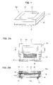
- FIG. 1 is a schematic perspective view showing an optical device according to a first embodiment of the present invention
- FIG. 2A is a plan view showing the optical device according to the first embodiment viewed from a transparent member side;
- FIG. 2B is a sectional view showing the optical device according to the first embodiment
- FIG. 3A is a plan view showing the configuration of the optical device wafer according to the first embodiment
- FIG. 3B is a sectional view showing the configuration of the optical device wafer according to the first embodiment
- FIG. 4A is a step sectional view showing the step of preparing a solid-state image element wafer in a method for manufacturing the optical device according to the first embodiment
- FIG. 4B is a step sectional view showing the step of applying a light-transmitting adhesive in the method for manufacturing the optical device according to the first embodiment
- FIG. 4C is a step sectional view showing the step of adhering a transparent member in the method for manufacturing the optical device according to the first embodiment
- FIG. 5A is a step sectional view showing the resin molding step in the method for manufacturing the optical device according to the first embodiment
- FIG. 5B is a step sectional view showing the configuration of the optical device wafer manufactured by the method for manufacturing the optical device according to the first embodiment
- FIG. 5C is a step sectional view showing the dividing step in the method for manufacturing the optical device according to the first embodiment
- FIG. 6A is a step sectional view showing the step of adhering a transparent member in a method for manufacturing an optical device according to a second embodiment
- FIG. 6B is a step sectional view showing the resin molding step in the method for manufacturing the optical device according to the second embodiment
- FIG. 6C is a step sectional view showing the dividing step in the method for manufacturing the optical device according to the second embodiment
- FIG. 7 is a sectional view showing a digital camera module according to a third embodiment
- FIG. 8 is a sectional view showing an endoscope module according to a fourth embodiment
- FIG. 9 is a sectional view showing an optical device according to a fifth embodiment.
- FIG. 10A is a step sectional view showing the step of adhering a transparent member in a method for manufacturing the optical device according to the fifth embodiment
- FIG. 10B is a step sectional view showing the resin molding step in the method for manufacturing the optical device according to the fifth embodiment
- FIG. 10C is a step sectional view showing the step of fabricating an optical device water in the method for manufacturing the optical device according to the fifth embodiment
- FIG. 10D is a step sectional view showing the step of removing a surface protective seal in the method for manufacturing the optical device according to the fifth embodiment
- FIG. 11 is a sectional view showing an optical device according to a sixth embodiment.
- FIG. 12 is a sectional view showing an optical device according to a seventh embodiment
- FIG. 13 is a sectional view showing an optical device according to an eighth embodiment.
- FIG. 14A is a plan view showing the configuration of an optical device according to a ninth embodiment viewed from the transparent member side;
- FIG. 14B is a sectional view showing the configuration of the optical device according to the ninth embodiment.
- FIG. 15A is a sectional view showing the configuration of the optical device wafer according to the ninth embodiment.
- FIG. 15B is a plan view showing the configuration of the optical device wafer according to the ninth embodiment.
- FIG. 16 is a sectional view showing a conventional solid-state image device.
- FIGS. 17A to 17G are step sectional views showing a method for manufacturing the conventional solid-state image device.
- FIG. 1 is a schematic perspective view showing an optical device according to the first embodiment of the present invention.
- FIGS. 2A and 2B are diagrams showing the configuration of the optic device;
- FIG. 2A is a plan view showing the optical device according to the first embodiment viewed from a transparent member side; and
- FIG. 2B is a sectional view showing the optical device according to the first embodiment, which is the sectional view taken along the line X-X in FIG. 2A .
- FIG. 2A shows a state in which part of a transparent member and molding resin have been removed.
- a solid-state image device is used, and the configuration of a solid-state image device 10 a (an example of optical devices) will be described referring to FIGS. 1 and 2 .
- the solid-state image device 10 a is equipped with a solid-state image element 11 a , which is an example of optical elements; a light transmitting member, such as a transparent member 12 ; and a molding resin 14 .
- an imaging region 16 a (an example of light receiving regions) formed in the vicinity of the center, and a peripheral circuit region 22 located around the imaging region 16 a are provided.
- micro lenses 25 are formed on each pixel arrayed.
- the peripheral circuit region 22 has a plurality of element electrodes 18 to connect peripheral circuits with an internal wiring 17 , and the internal wiring 17 is electrically connected to the element electrodes 18 .
- a plurality of electrodes for external connection 15 are provided on a back surface opposite to the major surface of the solid-state image element 11 a .
- the electrodes for external connection 15 are electrically connected to the element electrodes 18 via penetration electrodes 19 formed on a semiconductor substrate 20 .
- silicon silicon as the material of the semiconductor substrate 20 are described here, one of group III-V compounds and group II-VI compounds may also be used in consideration of application to semiconductor laser and light emitting diode.
- the transparent member 12 is adhered onto the major surface of the solid-state image element ha using a light transmitting adhesive, such as a light-transmitting adhesive 13 , and is disposed so as to coat the entire surface of the imaging region 16 a .
- a light transmitting adhesive such as a light-transmitting adhesive 13
- Upper and lower surfaces of the transparent member 12 are parallel to each other and are processed to be optical flat surfaces.
- Side surfaces of the transparent member 12 are perpendicular to the upper and lower surfaces, and have rectangular project planes. In the project planes of the transparent member 12 , four corners may be cut at an angle of about 45°, and each edge of one of or both of the upper and lower surfaces may be chamfered.
- the material of the transparent member 12 may be, for example, a borosilicate glass plate, and may be a low-pass filter consisting of one of a quartz plate and a calcite plate having birefringence properties to prevent moiré due to fringes in specific directions.
- a low-pass filter wherein quartz plates or calcite plates are adhered on both sides of an infrared cut filter so that birefringence properties intersect at right angles to one another, may be used.
- a transparent epoxy resin plate, an acrylic resin plate, and a transparent alumina plate can also be used.
- the thickness of the transparent member 12 when the borosilicate glass plate is used is within a range of 200 ⁇ m to 1000 ⁇ m, preferably within a range of 300 ⁇ m to 700 ⁇ m.
- the reason why the minimum thickness is 200 ⁇ m is to realize the size and thickness reduction so that, when the solid-state image device 10 a composed of the transparent member 12 , the light-transmitting adhesive 13 , the molding resin 14 , the solid-state image element 11 a , and the electrodes for external connection 15 is mounted, the height is not more than 500 ⁇ m; and the reason why the maximum thickness is 1000 ⁇ m is to realize a transmittance of at least 90% to incident light of a wavelength of 500 nm.
- the preferable thickness range is from 300 ⁇ m to 700 ⁇ m is that the thickness range makes it possible to produce the solid-state image device 10 a most stably using the present manufacturing technique, and a small and thin solid-state image device 10 a can be realized at low manufacturing costs by applying inexpensive general-purpose materials to the components.
- the thickness of each transparent member 12 must be determined taking the difference in transmittance into consideration; and in the case of quartz and calcite, since the distance of double image due to birefringence relates to the thickness of the transparent member 12 , the thickness must be determined taking into consideration the distance between pixels of the solid-state image element 11 a in addition to the difference in transmittance.
- the light-transmitting adhesive 13 is an optical light-transmitting adhesive used when the transparent member 12 is adhered on the imaging region 16 a , and may be, for example, an acrylic resin, an epoxy resin with resin composition having no absorption edge within the wavelength range of visible light, or a polyimide resin.
- the light-transmitting adhesive 13 has cured properties of lower refractive index than the micro lenses 25 formed on the imaging region 16 a , and the cured properties can be performed by one of or both of ultraviolet irradiation and heating.
- the molding resin 14 coats the side surfaces of the transparent member 12 , and the major surface (upper surface) of the solid-state image element 11 a excluding the region coated with the transparent member 12 .
- the molding resin 14 is a light shielding resin having a flat upper surface and a thickness being substantially the same as the transparent member 12 .
- biphenyl resins or silicone resins may also be used when a low-elasticity cured article is applied for reducing the thickness of the semiconductor substrate 20 or for improving the thermal impact resistance or moisture resistance of the solid-state image device 10 a.
- the molding resin 14 is composed of an epoxy resin, which is a major component, in a state in which semi-cured powder resin is in a tablet form; a curing agent; a curing promoting agent, powdered silica as an inorganic filler; a flame retardant; carbon black as a pigment; and a mold release.
- a liquid molding resin 14 composed of the above-described compounding components excluding the mold release is used.
- the selection and compounding quantity of the inorganic filler and pigment in the molding resin 14 used in the solid-state image device 10 a of the present embodiment are important for the warpage and light shielding of the solid-state image device 10 a . Therefore, it is necessary to suppress the warpage of the solid-state image device 10 a by compounding as much of the inorganic filler as possible insofar as the flow (viscosity) of the molten resin during molding is not affected to make the linear expansion coefficient approach the linear expansion coefficient of the solid-state image element 11 a and the transparent member 12 .
- high-purity silica produced by melting to remove crystallinity therefrom is processed in spheres of various diameters and is properly compounded.
- the incident light around the transparent member 12 is prevented from entering from the side surfaces of the transparent member 12 to become stray light.
- the pigment for example, carbon black of a tone having high light-shielding properties is used to prevent a part of the incident light from the above the molding resin 14 from reaching the p-n junction and the gate portions of the passive element and active element on the major surface of the solid-state image element 11 a so as to avoid the malfunction of the solid-state image element 11 a . It is also important to select the material having a particle diameter that can increase the compounding quantity and having a low polarizing property.
- Conductive electrodes 21 for mounting on the circuit substrate of electronic device are formed on the electrodes for external connection 15 .
- the conductive electrodes 21 may be, for example, solder balls, or a resin ball with a conductive film formed on the surface or may be bumps (stud bumps) formed by wire bonding.
- solder balls solder materials having various compositions, such as Sn—Ag—Cu, Sn—Ag—Bi, and Zn—Bi, can be used.
- solder materials having various compositions, such as Sn—Ag—Cu, Sn—Ag—Bi, and Zn—Bi, can be used.
- an electrically conductive adhesive can also be used for mounting.
- the conductive electrodes 21 can be formed by supplying a solder paste onto the electrodes for external connection 15 using, for example, screen printing, and reflowing.
- the imaging region 16 a As described above, by coating at least the imaging region 16 a with the transparent member 12 , and molding with the molding resin 14 the side surfaces of the transparent member 12 and the surface of the peripheral circuit region 22 not coated with the transparent member 12 , since the imaging region 16 a can be protected by the transparent member 12 and the peripheral circuit region 22 can be protected by the molding resin 14 , the mechanical damage on the major surface of the solid-state image device 10 a can be prevented. Furthermore, since the entire major surface of the solid-state image element 11 a is coated with the molding resin 14 and the light-transmitting adhesive 13 , the strength of the solid-state image element 11 a can be prevented from lowering.
- the solid-state image device 10 a having excellent moisture resistance and high reliability can be fabricated.
- the molding resin 14 on the side surfaces of the transparent member 12 , flare, smear, or the like caused by stray light generated by the invasion of external reflected light from the side surfaces of the transparent member 12 can be prevented. Furthermore, since the solid-state image device 10 a requires no housing, and the transparent member 12 is directly adhered on the major surface of the solid-state image element 11 a with the light-transmitting adhesive 13 , the reduction of the size and thickness of the chip can be realized.
- FIGS. 3A and 3B are diagrams of the solid-state image device wafer 30 wherein a plurality of solid-state image devices 10 a are arrayed vertically and horizontally;
- FIG. 3A is a plan view showing the configuration of the optical device wafer according to the first embodiment;
- FIG. 3B is a sectional view taken along the line X-X in FIG. 3A showing the configuration of the optical device wafer according to the first embodiment.
- the solid-state image device wafer 30 is an embodiment of the optical device wafer, and a solid-state image device wafer will be described as an example.
- the solid-state image device wafer 30 is composed of a plurality of the solid-state image elements 11 a arranged vertically and horizontally at even intervals; the transparent members 12 disposed on the micro lenses formed in the imaging region 16 a of each solid-state image element 11 a ; the light-transmitting adhesive 13 for adhering the solid-state image elements 11 a to the transparent members 12 ; and the molding resin 14 for forming a light-shielding layer between the adjoining transparent members 12 on the major surface of the wafer.
- the solid-state image device wafer 30 may be resin molded without adhering the transparent member 12 on the imaging region 16 a of the solid-state image element 11 a rejected in the electrical test or the optical test; alternatively, resin molding may be carried out after adhering an inexpensive dummy block having the same size as the transparent member 12 for maintaining the flatness of the upper surface of the molding resin 14 during resin molding.
- the dummy block is formed of a material, such as resins and silicones.
- the solid-state image device wafer 30 can be fabricated in a wafer form without wasting the expensive transparent members 12 by adhering the transparent members 12 only on the imaging regions 16 a of the solid-state image elements 11 a accepted in the test, or by adhering the dummy blocks on the locations of the solid-state image elements ha rejected in the test as described above, a thin solid-state image device wafer 30 can be realized at low costs.
- FIG. 4A is a step sectional view showing the step of preparing a solid-state image element wafer in a method for manufacturing the optical device according to the first embodiment
- FIG. 4B is a step sectional view showing the step of applying the light-transmitting adhesive in the method for manufacturing the optical device according to the first embodiment
- FIG. 4C is a step sectional view showing the step of adhering the transparent member in the method for manufacturing the optical device according to the first embodiment.
- FIG. 5A is a step sectional view showing the resin molding step in the method for manufacturing the optical device according to the first embodiment
- FIG. 5B is a step sectional view showing the configuration of the optical device wafer manufactured by the method for manufacturing the optical device according to the first embodiment
- FIG. 5C is a step sectional view showing the dividing step in the method for manufacturing the optical device according to the first embodiment.
- FIGS. 1-10 are sectional views showing the steps from molding with the molding resin 14 the region excluding the transparent member 12 on the major surface of the semiconductor substrate 20 to fabricate the solid-state image device wafer 30 , to dividing the solid-state image device wafer 30 into a plurality of the solid-state image devices 10 a to form conductive electrodes 21 .
- a solid-state image device is also used for the description as an example of optical devices.
- a solid-state image element wafer 40 (an example of optical element wafers) including the semiconductor substrate 20 on which the plurality of solid-state image elements 11 a are vertically and horizontally arrayed is prepared. Every solid-state image element 11 a has been subjected to electrical and optical tests in the wafer state.
- FIG. 4B shows the step of applying the light-transmitting adhesive 13 .
- the light-transmitting adhesive 13 is applied onto the micro lenses 25 in the imaging region 16 a situated in the central portion of each solid-state image element 11 a by, for example, screen printing to form a coating film.
- the light-transmitting adhesive 13 supplied onto a mask 41 is flowed onto the imaging region 16 a through the pattern of the mask 41 using a squeegee 42 .
- the curing property may be heat setting, or may be both ultraviolet setting and heat setting properties.
- the material for the light-transmitting adhesive 13 may be one of an epoxy resin and an acrylic resin, or may be a polyimide resin.
- the method for forming the coating film of the light-transmitting adhesive 13 may be one of a drawing method, a potting method, and a stamping method; and a semi-cured prepreg sheet may also be used.
- the coating film of the light-transmitting adhesive 13 may be formed only on the location of the solid-state image elements 11 a accepted in the test.
- FIG. 4C is a sectional view showing the step of adhering the light transmitting member, such as the transparent member 12 .
- the transparent member 12 such as borosilicate glass divided into pieces having a size to coat the entire surface of the imaging region 16 a is placed on the imaging region 16 a of each solid-state image element 11 a to which the light-transmitting adhesive 13 has been applied of the solid-state image element wafer 40 , so as not to introduce the air.
- the transparent member 12 may be placed on the light-transmitting adhesive 13 in a reduced-pressure atmosphere while defoaming.
- the transparent member 12 may be adhered to the micro lenses 25 in the imaging region 16 a by aligning the transparent member 12 to the surface of the imaging region 16 a in parallel at the proper location on the imaging region 16 a , and radiating ultraviolet beams having predetermined optical energy, or by heating after ultraviolet irradiation.
- the transparent member 12 may be any of quartz, calcite, alumina, and transparent resins.
- FIG. 5A is a sectional view showing the step of resin molding.
- the side surfaces of the transparent member 12 and the major surface of the solid-state image element 11 a in the region excluding the transparent member 12 are coated with the epoxy molding resin 14 to form a layer of the molding resin 14 having the same thickness as the thickness of the transparent member 12 by transfer molding using a mold for resin molding 51 .
- the material for the molding resin 14 may be biphenyl resins or silicone resins.
- the mold for resin molding 51 is composed of an upper mold 52 and a flat lower mold 53 , and is preheated to a temperature range of 160° C. to 210° C. at which the molding resin 14 is melted, preferably, a temperature range of 175° C. to 195° C.
- a thin release sheet 54 a made of tensioned tetrafluoroethylene resin is disposed in the lower mold 53 .
- the upper mold 52 is equipped with a cavity (not shown) having a depth substantially the same as the total thickness of the transparent member 12 and the solid-state image element wafer 40 .
- the upper mold 52 is constituted so as to accommodate the solid-state image element wafer 40 on the surface thereof, and a thin release sheet 54 b made of tensioned tetrafluoroethylene resin is disposed in the upper mold 52 .
- the solid-state image element wafer 40 on which the transparent member 12 is adhered is placed on the predetermined location in the lower mold 53 via the release sheet 54 a .
- the upper mold 52 is closed until the upper surface of the transparent member 12 on the major surface side and the electrodes for external connection 15 on the back side are compressed to the release sheets 54 a and 54 b , respectively.
- the molten molding resin 14 is injected into the cavity, and the upper and lower molds 51 are held in the closed (clamped) state until the molding resin 14 is cured in the cavity.
- the upper and lower molds 51 are opened after a predetermined time, and the resin-molded solid-state image element wafer 40 , i.e., the solid-state image device wafer 30 (an example of optical device wafers) is taken out as shown in FIG. 5B .
- the time of holding the solid-state image element wafer 40 in the mold for resin molding 51 is the time until the cross-linking reaction of the molding resin 14 is progressed to reach a strength so that resistance to deformation is obtained.
- the release sheets 54 a and 54 b may be formed of other flexible heat-resistant resin films having no reactive groups.
- the solid-state image device wafer 30 after the resin molding step is divided into individual solid-state image devices 10 a by cutting along the dividing line L using a dicer.
- stealth dicing using a laser may also be used.
- the conductive electrodes 21 are joined on the electrodes for external connection 15 of each solid-state image device 10 a .
- this step to join solder balls as an example of the conductive electrodes 21 to a land plane on the back surface of the solid-state image device 10 a , by applying a flux onto the land plane, placing solder balls thereon, and passing the solid-state image device 10 a through a reflowing furnace set to a predetermined temperature distribution to join the solder balls onto the land, the solid-state image device 10 a can be realized.
- the conductive electrodes 21 of solder balls are formed after dividing the solid-state image device wafer 30 into individual solid-state image devices 10 a in the above-described manufacturing method, the conductive electrodes 21 may be formed before dividing the solid-state image device wafer 30 , and thereafter, the solid-state image device wafer 30 may be divided into individual solid-state image devices 10 a .
- the conductive electrodes 21 may be plated bumps wherein thin gold films are formed on copper or nickel bases, or may be stud bumps formed by gold-ball bonding.
- a plurality of solid-state image devices 10 a can be collectively formed by applying processing in the wafer state of the first embodiment, and the manufacturing method wherein integral resin molding in the wafer state is performed using the mold for resin molding 51 . Furthermore, the reduction of facility investment by compacting the production line, and the reduction of the thickness of the solid-state image devices 10 a can be realized. Since the solid-state image element wafer 40 can be fabricated in the wafer state without wasting the expensive transparent member 12 by adhering the transparent member 12 only to the solid-state image elements 11 a accepted in the test, or by connecting dummy blocks to the locations of the solid-state image elements 11 a rejected in the test, an inexpensive solid-state image device 10 a can be realized.
- the upper surface of the transparent member 12 of the solid-state image device 10 a may be aligned with the upper surface of the molding resin 14 (same height)
- the upper surface of the transparent member 12 may be higher than the upper surface of the molding resin 14 by burying (impressing) the upper surface and the upper ends of the sides of the transparent member 12 in the release sheet 54 b when the mold 51 is closed as shown in FIG. 5A .
- the second embodiment is a manufacturing method in which resin molding of a solid-state image device wafer 30 is performed using not the mold for resin molding in the first embodiment, but screen printing.
- FIG. 6A is a step sectional view showing the step of adhering a transparent member in the method for manufacturing an optical device according to the second embodiment; and a solid-state image element wafer 40 is manufactured and prepared by the steps shown in the above-described FIG. 4 .
- FIG. 6B is a step sectional view showing the resin molding step in the method for manufacturing the optical device according to the second embodiment; and
- FIG. 6C is a step sectional view showing the dividing step in the method for manufacturing the optical device according to the second embodiment.
- a transparent member 12 and the major surface (upper surface) of the solid-state image element wafer 40 in the region excluding the transparent member 12 are coated with a liquid epoxy molding resin 14 by the screen printing using a screen printer to form a layer of the molding resin 14 having the same thickness as the transparent member 12 (i.e., flush with the upper surface of the transparent member 12 ).
- the material for the molding resin 14 may be a biphenyl resin or a silicone resin.
- the screen printer is equipped with a metal mask for printing 61 wherein a pattern capable of applying the liquid molding resin 14 to the region excluding the transparent member 12 is formed.
- the sample table is preheated to a temperature in a range of 50° C. to 100° C., preferably of 65° C. to 85° C. at which the liquid molding resin 14 has a low viscosity. Then, a predetermined amount of the liquid molding resin 14 supplied onto the surface of the metal mask for printing 61 is poured from the pattern of the metal mask for printing 61 using a squeegee 62 and is applied to the region excluding the transparent member 12 .
- the solid-state image element wafer 40 may be kept horizontal in a clean environment until the liquid molding resin 14 is sufficiently spread. Alternatively, the solid-state image element wafer 40 may be kept horizontal in a reduced-pressure atmosphere while removing the air contained in the liquid molding resin 14 .
- the solid-state image element wafer 40 is kept horizontal in a curing oven heated to a temperature in a range of 160° C. to 210° C., preferably of 175° C. to 195° C. for a predetermined time to cure the molding resin 14 .
- the molding resin 14 may be cured in two steps; preliminary curing and final curing. The molding resin 14 is heated until the cross-linking reaction is progressed and the strength to resist deformation is obtained.
- the solid-state image device wafer 30 after the above-described resin molding step is divided along the dividing line L into individual solid-state image devices 10 a using a dicer, and the step of joining conductive electrodes 21 (refer to FIG. 5C ) is performed to realize the solid-state image devices 10 a.
- FIG. 7 is a sectional view showing a digital camera module according to the third embodiment; specifically, a sectional view showing a digital camera module 70 , which is an application example of a solid-state image device lea to electronic devices.
- the camera module 70 has a configuration wherein conductive electrodes 21 of the solid-state image device 10 a are joined to mounting lands 71 a disposed on the central portion of the upper surface of a glass-epoxy wiring substrate 71 , and the mounting height H of the solid-state image device 10 a is within a range of about 0.5 mm to 0.7 mm.
- the wiring substrate 71 may also be a flexible wiring substrate composed of polyimide and the like.
- a fixed housing tube 72 having an opening wider than an imaging region 16 a of the solid-state image device 10 a is disposed and is adhered at a predetermined location on the upper surface of the wiring substrate 71 .
- a sliding housing tube 73 equipped with a lens 76 is inserted, and after the focal point is adjusted, the sliding housing tube 73 is adhered to the fixed housing tube 72 using an adhesive (not shown).
- a configuration wherein a space is secured above the solid-state image device 10 a in the fixed housing tube 72 , and a low-pass filter 74 and a light shielding plate 75 are disposed in the space may also be used.
- the height from the upper end of the sliding housing tube 73 to the upper surface of the wiring substrate 71 can be lowered by designing the mounting height H of the thin solid-state image device 10 a to be low, a thin digital camera can be realized. Furthermore, by securing a space above the solid-state image device 10 a in the fixed housing tube 72 , and disposing the low-pass filter 74 and the light shielding plate 75 in the space, a high-quality thin digital camera generating no moiré can be realized.
- FIG. 8 is a sectional view showing an endoscope module according to the fourth embodiment, and shows the cross section of an endoscope module 80 for disaster, for investigating buried cultural properties and for medical treatments as an application example of a solid-state image device 10 a to electronic devices.
- the housing tube portion of the endoscope module 80 for disaster, for investigating buried cultural properties and for medical treatments has a configuration wherein conductive electrodes 21 of the solid-state image device 10 a are joined to a flexible wiring substrate 81 and mounting lands 81 a disposed on a surface close to the end portion of the flexible wiring substrate 81 , and the mounting height H of the solid-state image device 10 a is within a range of about 0.5 mm to 0.7 mm.
- a semiconductor device for driving 85 and passive electronic parts 86 of peripheral circuits are joined to the joining side of the solid-state image device 10 a close to the center portion of the flexible wiring substrate 81 and the mounting land on the opposite surface, respectively; and external electrodes 87 of the flexible wiring substrate 81 are formed on the surface opposite to the joining side of the solid-state image device 10 a close to the other end portion of the flexible wiring substrate 81 , which are electrically connected by wirings and through-holes on the flexible wiring substrate 81 .
- the flexible wiring substrate 81 is bent at two locations so that the cross section has an inverted N-shape, and held in a housing tube 82 .
- the center portion of the flexible wiring substrate 81 may have a configuration wherein back surfaces of a plurality of the flexible wiring substrates to which electronic parts are joined are laminated so as to form a circuit for imparting high added value functions to a surface of the other flexible wiring substrate.
- a small, thin, and high-quality endoscope module 80 for disaster, for investigating buried cultural properties and for medical treatments, excellent in moisture resistance and preventing deterioration of strength can be realized.
- FIG. 9 is a sectional view showing the optical device according to the fifth embodiment.
- a solid-state image device 90 will be described.
- the solid-state image device 90 is equipped with a solid-state image element 11 a , a transparent member 12 adhered on an imaging region 16 a of the solid-state image element 11 a using a light-transmitting adhesive 13 , and a light shielding molding resin 14 that coats the side surfaces of the transparent member 12 and the major surface of the solid-state image element 11 a excluding the region coated by the transparent member 12 .
- the thickness of the molding resin 14 is larger than the thickness of the transparent member 12 by a range of 20 ⁇ m to 150 ⁇ m, preferably a range of 50 ⁇ m to 100 ⁇ m. Thereby, the upper surface of the molding resin 14 is formed to be higher than the upper surface of the transparent member 12 .
- the operation of the above-described configuration will be described. Since the upper end portion of the molding resin 14 is projected from the upper surface of the transparent member 12 , the lowering of mechanical strength due to the thickness reduction of a semiconductor substrate 20 can be prevented by the thickened molding resin 14 . Flares and smears caused by stray light generated by the invasion of external reflected light from the side surfaces of the transparent member 12 can also be prevented. Furthermore, since the solid-state image device 90 does not require housing, and the transparent member 12 is directly adhered on the major surface of the solid-state image element 11 a , the reduction of the size and thickness of chips can be realized. Since the side surfaces of the transparent member 12 are completely coated with the molding resin 14 , a solid-state image device 90 that excels in optical properties can be realized.
- FIGS. 10A to 10D show sectional views illustrating the step of resin molding of the solid-state image element 11 a , the step of making individual solid-state image devices 90 , and the step of peeling off a surface protective seal 91 in the method. Since the step of preparing a solid-state image element wafer 40 formed of a plurality of the solid-state image elements 11 a vertically and horizontally arranged at even intervals, and the step of forming conductive electrodes 21 on electrodes for external connection 15 are the same as those in the first embodiment shown in FIG. 4A and FIG. 5C , respectively, the detailed description thereof will be omitted here.
- FIG. 10A is a step sectional view showing the step of adhering the transparent member in the method for manufacturing the optical device according to the fifth embodiment, and is a sectional view showing the step of adhering the transparent member 12 on the imaging region 16 a of each solid-state image element 11 a .
- Transparent members 12 made of borosilicate glass are placed on the imaging region 16 a of each solid-state image element 11 a to which the light-transmitting adhesive 13 is applied of the solid-state image element wafer 40 so as not to introduce the air.
- the transparent member 12 has a size to coat the entire surface of the imaging region 16 a , and the surface protective seal 91 has previously been adhered on the upper surface of the transparent member 12 (major surface opposite to the solid-state image element 11 a ). Thereby, the adhesion of dust on the upper surface of the transparent member 12 can be avoided.
- the transparent member 12 may also be placed on the light-transmitting adhesive 13 while defoaming in a reduced-pressure atmosphere.
- the transparent member 12 is aligned in parallel with the surface of the imaging region 16 a at the proper location of the imaging region 16 a , and ultraviolet beams having a predetermined optical energy are radiated so as to cure the light-transmitting adhesive 13 to adhere the transparent member 12 on the micro lenses 25 of the imaging region 16 a .
- the transparent member 12 may be adhered by heating after the irradiation of ultraviolet beams.
- the transparent member 12 may be made of any of quartz, calcite, alumina, and a transparent resin.
- FIG. 10B is a step sectional view showing the resin molding step in the method for manufacturing the optical device according to the fifth embodiment. Since this step can be carried out by transfer molding using a mold 51 as in the first embodiment shown in FIG. 5A , the detailed description will be omitted. In this step, however, since the surface protective seal 91 is adhered on the surface of the transparent member 12 , when an upper mold 52 and a lower mold 53 of the mold 51 are clamped, the surface protective seal 91 is compressed to a release sheet 54 b on the upper mold 52 .
- FIG. 10C is a step sectional view showing the step of fabricating the optical device wafer in the method for manufacturing the optical device according to the fifth embodiment
- the resin-molded solid-state image element wafer 40 that is a solid-state image device wafer 30 (an example of optical device wafers)
- the upper surface of the surface protective sea 91 is formed to be substantially flush (the same height) with the upper surface of the molding resin 14 .
- the solid-state image device wafer 30 is cut along the dividing line L with a dicer into individual solid-state image devices 90 .
- the transparent member 12 is coated with the surface protective seal 91 , the transparent member 12 is not damaged in the dicing step.
- FIG. 10D is a step sectional view showing the step of removing the surface protective seal in the method for manufacturing the optical device according to the fifth embodiment, and is the step of peeling off the surface protective seal 91 on the transparent member 12 .
- the surface protective seal 91 is peeled off and removed from the transparent member 12 , and the upper surface of the clean transparent member 12 is exposed.
- each solid-state image device 90 is joined to the electrodes for external connection 15 of each solid-state image device 90 . Since the configuration for applying the solid-state image device 90 obtained in the fifth embodiment to digital cameras or endoscopes for disaster, for investigating buried cultural properties and for medical treatments to fabricate electronic devices is the same as in the electronic devices described in the third and fourth embodiments, the description thereof will be omitted here.
- FIG. 11 is a sectional view showing an optical device according to the sixth embodiment.
- the same elements as in FIG. 2 of the above-described first embodiment are denoted by the same reference numerals and characters, and the description thereof will be omitted here.
- a transparent member 93 has a size to coat the entire surface of an imaging region 16 a on which micro lenses 25 of a solid-state image element 11 a are formed, and both upper and lower surfaces of the transparent member are processed to be optically flat and are parallel to each other.
- a side surface of the transparent member 93 has a step 93 c consisting of an upper step 93 a and a lower step 93 b .
- the projection plane of the lower step 93 b is rectangular and larger than the imaging region 16 a of the solid-state image element 11 a both in length and width, and larger than the projection plane of the upper step 93 a .
- the projection plane of the upper step 93 a is rectangular and has the substantially same size as the imaging region 16 a of the solid-state image element 11 a .
- a step plane 93 d of the upper step 93 a and the lower step 93 b is formed above half the thickness of the transparent member 93 .
- the edges of the upper step 93 a may be chamfered.
- four corners may be cut at about 45°, and in addition, the edges of one of or both upper and lower surfaces may be chamfered.
- the material of the transparent member 93 is a borosilicate glass plate, a low-pass filter formed of either quartz or calcite may be used, and a transparent epoxy resin, acrylic resin, or transparent alumina may also be used.
- the thickness and transmissivity of the transparent member 93 are the same as in the first embodiment.
- a layer of a molding resin 14 coats the side surface of the upper step 93 a , the side surface of the lower step 93 b and the step plane 93 d of the transparent member 93 , and the projection plane of the upper step 93 a has the substantially same size as the imaging region 16 a of the solid-state image element 11 a , the same effect as when a light-shielding plate is disposed on the transparent member 93 can be obtained in addition to the advantage obtained in the first embodiment.
- the adhesion area of the transparent member 93 and the molding resin 14 is enlarged, the delamination of the transparent member 93 from the molding resin 14 can be prevented, and the invasion of moisture from the boundary between the transparent member 93 and the molding resin 14 can also be prevented.
- FIG. 12 is a sectional view showing an optical device according to the seventh embodiment, and specifically, a sectional view showing a solid-state image device 95 according to the seventh embodiment, which is a modification of the sixth embodiment.
- the projected plane of a lower step 93 b of a transparent member 93 has a rectangular shape of the substantially same size as an imaging region 16 a , and is smaller than the projected plane of an upper stage 93 a.
- the same effect as when a light-shielding plate is disposed on the transparent member 93 can be obtained, and since the adhesion area of the transparent member 93 and a molding resin 14 is enlarged, the delamination of the transparent member 93 from the molding resin 14 can be prevented, and the invasion of moisture from the boundary between the transparent member 93 and the molding resin 14 can also be prevented in addition to the advantage obtained in the first embodiment.
- the step 93 c is formed on the side surface of the transparent member 93
- the side surfaces of the transparent member 93 may be tilted as shown in a sectional view of an optical device according to the eighth embodiment in FIG. 13 .
- FIG. 14A is a plan view showing the configuration of an optical device according to the ninth embodiment viewed from a transparent member side; and FIG. 14B is a sectional view showing the configuration of the optical device according to the ninth embodiment, and is a sectional view taken along the line 3 A- 3 A′.
- FIG. 15A is a sectional view showing the configuration of an optical device wafer according to the ninth embodiment; and FIG. 15 D is a plan view showing the configuration of the optical device wafer according to the ninth embodiment.
- an LED device 10 b the configuration of an LED device 10 b will be described using a light emitting element, particularly an LED (light emitting diode) device 10 b as an example of optical devices referring to FIGS. 14A , 14 B, 15 A and 15 B.
- the ninth embodiment can also be applied to a similar light emitting element, such as a surface emitting laser.
- the LED device 10 b is equipped with an LED element 11 b being an example of optical elements, a transparent member 12 , and a molding resin 14 .
- a light emitting region 16 b is formed on the major surface of the LED element 11 b and an element electrode 18 is provided around the light emitting region 16 b .
- the element electrode 18 is electrically connected to the light emitting region 16 b , and on the back surface opposite to the major surface of the LED element 11 b , a plurality of electrodes for external connection 15 are provided.
- these electrodes for external connection 15 are normally composed of two terminals: one is conducted from the element electrode 18 to the lower surface through a penetration electrode 19 , and the other is directly connected to the back surface of the LED element 11 b to constitute the electrode for external connection 15 .
- group III-V compounds and group II-VI compounds are mainly used on a semiconductor laser and LED (light emitting diode) and in the case of the light emitting diode, GaN substrate and the like are often used.
- the transparent member 12 is adhered on the major surface of the LED element 11 b using a light-transmitting adhesive, such as a light-transmitting adhesive 13 , and is disposed so as to coat the entire surface of the light emitting region 16 b .
- the end surface of the transparent member 12 has no molding resin provided on three of four sides, and the transparent member 12 is exposed on the end surface.
- Such a form can be produced if the transparent member 12 is made to be reed-shaped in the manufacturing step, because a plurality of the LED elements 11 b can be easily fabricated in the wafer or block state.
- a glass plate can be used as the material for the transparent member 12
- an organic transparent substrate such as a transparent acrylic resin, a transparent silicone resin, and a transparent epoxy resin should be used for ease of dicing.
- the thickness of the transparent member 12 is within a range of 10 ⁇ m to 100 ⁇ m, preferably of 20 ⁇ m to 80 ⁇ m.
- the reason why the minimum thickness is 10 ⁇ m is that the size and thickness reduction is realized so that the mounting height of the LED (light emitting diode) device composed of the transparent member 12 , the light-transmitting adhesive 13 , the molding resin 14 , the LED element 11 b and the electrode for external connection 15 when mounted is 100 ⁇ m or less; and the reason why the maximum thickness is 100 ⁇ m is that the size and thickness reduction to 300 ⁇ m or less is realized.
- the preferable range is from 20 ⁇ m to 80 ⁇ m is that this range of thickness is the thickness enabling the LED (light emitting diode) device 10 b to be most stably produced using the existing manufacturing technology, and for realizing an inexpensive, small and thin LED (light emitting diode) device 10 b by applying inexpensive general-purpose materials as the components.
- the thickness must be determined considering the transmission efficiency of each transparent member 12 .
- the light-transmitting adhesive 13 is an optically light-transmitting adhesive used when the transparent member 12 is fixed on the light emitting region 16 b , and can be, for example, acrylic resins, epoxy resins compounded so as to have no absorption end within the wavelength range of visible light, or polyimide resins.
- the light-transmitting adhesive 13 can be cured by ultraviolet irradiation, heating, or the combination thereof, and the cured light-transmitting adhesive 13 has a low refraction index.
- the molding resin 14 particularly coats the element electrode 18 on the major surface of the LED element 11 b , and is a resin formed to have a flat upper surface, and the thickness of the molding resin 14 is substantially the same as the total thickness of the transparent member 12 and the light-transmitting adhesive 13 .
- considerations for light-shielding properties are not required, and it is only necessary to firmly protect the element electrode 18 from moisture and mechanical stress.
- an epoxy resin is mainly used as the material for the molding resin 14 , when a low-elasticity cured article is used for improving resistance to thermal shock and moisture, biphenyl resins or silicone resins may also be used.
- the transparent member 12 and the light-transmitting adhesive 13 may be adhered on the entire major surface of the LED element 11 b .
- the total thickness of the transparent member 12 and the light-transmitting adhesive 13 must combine the light emitting properties of the LED (light emitting diode) device 10 b , and the properties of moisture resistance, heat resistance and the like.
- the mechanical damage on the major surface of the LED (light emitting diode) device 10 b can be prevented. Also since the entire major surface of the LED (light emitting diode) device 10 b is coated with the molding resin 14 and the light-transmitting adhesive 13 , the strength lowering of the LED (light emitting diode) device 10 b can be prevented.
- the LED (light emitting diode) device 10 b does not require as high reliability as the above-described solid-state image device 10 a , it is not so required to firmly prevent the invasion of moisture from the adhesion boundary between the transparent member 12 and the LED element 11 b compared with the solid-state image device 10 a .
- the reason for this is that although moisture resistance is important for the solid-state image device 10 a because micro lenses 25 are disposed on the imaging region 16 a , the LED (light emitting diode) device 10 b does not require micro lenses.
- the number of electrodes for external connection 15 is much smaller compared with the solid-state image device 10 a . Normally, the solid-state image device 10 a has several to several tens of pins.
- an LED (light emitting diode) or a surface emitting laser generally has two pins, or three pins including a pin for a grounding electrode and the like.
- the size of the solid-state image device 10 a is a maximum about 10 mm ⁇ 10 mm
- the size of the LED (light emitting diode) device 10 b is about 0.1 mm ⁇ 0.1 mm to 1.0 mm ⁇ 1.0 mm. Therefore, even if the end surface of the transparent member 12 has no molding resin and is exposed, the LED (light emitting diode) device 10 b is sufficient for practical use.
- the transparent member 12 can be made to be reed-shaped in the manufacturing step, the LED elements 11 b can be fabricated at lower costs.
- FIGS. 15A and 15B show diagrams illustrating the state in which a plurality of the LED (light emitting diode) devices 10 b are vertically and horizontally arranged;
- FIG. 15 A is a sectional view, and
- FIG. 15B is a plan view viewed from the transparent member 12 side in FIG. 15 A.
- the state is constituted by the plurality of LED (light emitting diode) devices 10 b , the transparent members 12 disposed on the LED elements 11 b , the light-transmitting adhesive 13 for adhering the LED elements 11 b to the transparent members 12 , and the molding resin 14 for molding the element electrodes 18 .
- a wafer or block on which the plurality of LED (light emitting diode) devices 10 b are formed is divided along the dividing lines L, and only accepted products are transferred to the next step.
- the LED (light emitting diode) devices 10 b rejected at the electrical or optical test are discarded.
- the wafer or block is cut using a dicing blade fabricated by solidifying diamond abrasive grains with a bonding material at a high-speed rotation (1,000 to 30,000 rpm).
- a method for dividing using a laser may also be used.
- the transparent members 12 are made of glass plates, since cracks are easily produced, if the thickness portions of the transparent members 12 are cut using the laser, and the thickness portions of the LED elements 11 b are cut using the dicing blade, a high-quality LED (light emitting diode) device 10 b without end surface cracking can be obtained.
- the suitable mounting height of the LED (light emitting diode) device 10 b is not less than 100 ⁇ m.
- the suitable mounting height of the LED (light emitting diode) device 10 b is less than 100 ⁇ m.
- the most suitable mounting height is less than 50 ⁇ m. The reason for this is that if the mounting height is less than 50 ⁇ m, for example, if the total thickness of the LED (light emitting diode) device 10 b is 30 ⁇ m, it is not required to repeat the radiation of laser beams multiple times, and the wafer can be divided by one radiation.
Abstract
Description
Claims (15)
Priority Applications (1)
| Application Number | Priority Date | Filing Date | Title |
|---|---|---|---|
| US13/193,075 US8455902B2 (en) | 2007-02-05 | 2011-07-28 | Optical device and method for manufacturing optical device, and camera module and endoscope module equipped with optical device |
Applications Claiming Priority (4)
| Application Number | Priority Date | Filing Date | Title |
|---|---|---|---|
| JP2007024945 | 2007-02-05 | ||
| JP2007-024945 | 2007-02-05 | ||
| JP2007-270759 | 2007-10-18 | ||
| JP2007270759A JP2008219854A (en) | 2007-02-05 | 2007-10-18 | Optical device, optical device wafer, method for manufacturing them, and camera module and endoscope module equipped with optical device |
Related Child Applications (1)
| Application Number | Title | Priority Date | Filing Date |
|---|---|---|---|
| US13/193,075 Division US8455902B2 (en) | 2007-02-05 | 2011-07-28 | Optical device and method for manufacturing optical device, and camera module and endoscope module equipped with optical device |
Publications (2)
| Publication Number | Publication Date |
|---|---|
| US20080185603A1 US20080185603A1 (en) | 2008-08-07 |
| US8013350B2 true US8013350B2 (en) | 2011-09-06 |
Family
ID=39675388
Family Applications (2)
| Application Number | Title | Priority Date | Filing Date |
|---|---|---|---|
| US11/968,763 Expired - Fee Related US8013350B2 (en) | 2007-02-05 | 2008-01-03 | Optical device and method for manufacturing optical device, and camera module and endoscope module equipped with optical device |
| US13/193,075 Active 2028-06-23 US8455902B2 (en) | 2007-02-05 | 2011-07-28 | Optical device and method for manufacturing optical device, and camera module and endoscope module equipped with optical device |
Family Applications After (1)
| Application Number | Title | Priority Date | Filing Date |
|---|---|---|---|
| US13/193,075 Active 2028-06-23 US8455902B2 (en) | 2007-02-05 | 2011-07-28 | Optical device and method for manufacturing optical device, and camera module and endoscope module equipped with optical device |
Country Status (1)
| Country | Link |
|---|---|
| US (2) | US8013350B2 (en) |
Cited By (12)
| Publication number | Priority date | Publication date | Assignee | Title |
|---|---|---|---|---|
| US20100117175A1 (en) * | 2008-11-07 | 2010-05-13 | Oki Semiconductor., Ltd. | Semiconductor module |
| US20100148292A1 (en) * | 2008-11-07 | 2010-06-17 | Panasonic Corporation | Semiconductor device |
| US20110073975A1 (en) * | 2009-09-30 | 2011-03-31 | Kabushiki Kaisha Toshiba | Semiconductor device, electronic apparatus, and manufacturing methods thereof |
| US20110089464A1 (en) * | 2009-10-15 | 2011-04-21 | Advanced Optoelectronic Technology Inc. | Light emitting diode package and method of fabricating the same |
| US20110163328A1 (en) * | 2008-01-23 | 2011-07-07 | Panasonic Corporation | Optical semiconductor device |
| US20110234893A1 (en) * | 2010-03-24 | 2011-09-29 | Kabushiki Kaisha Toshiba | Solid state imaging device, camera module, and method for manufacturing solid state imaging device |
| US20110298077A1 (en) * | 2003-09-17 | 2011-12-08 | Round Rock Research, Llc | Methods of fabrication of package assemblies for optically interactive electronic devices and package assemblies therefor |
| US20130037831A1 (en) * | 2011-08-10 | 2013-02-14 | Heptagon Micro Optics Pte. Ltd. | Opto-Electronic Module and Method for Manufacturing The Same |
| US20180006070A1 (en) * | 2015-02-13 | 2018-01-04 | Sony Corporation | Image sensor, method of manufacturing the same, and electronic apparatus |
| EP3281923A1 (en) | 2016-08-03 | 2018-02-14 | Shin-Etsu Chemical Co., Ltd. | Synthetic quartz glass lid and optical device package |
| EP3354633A1 (en) | 2017-01-31 | 2018-08-01 | Shin-Etsu Chemical Co., Ltd. | Synthetic quartz glass lid precursor, synthetic quartz glass lid, and preparation methods thereof |
| US11381767B2 (en) * | 2017-10-20 | 2022-07-05 | Panasonic Intellectual Property Management Co., Ltd. | Solid-state imaging device having electronic components mounted between a main substrate and an imaging element |
Families Citing this family (31)
| Publication number | Priority date | Publication date | Assignee | Title |
|---|---|---|---|---|
| US8814779B2 (en) | 2006-12-21 | 2014-08-26 | Intuitive Surgical Operations, Inc. | Stereoscopic endoscope |
| US8556807B2 (en) * | 2006-12-21 | 2013-10-15 | Intuitive Surgical Operations, Inc. | Hermetically sealed distal sensor endoscope |
| KR100871707B1 (en) * | 2007-03-30 | 2008-12-05 | 삼성전자주식회사 | Wafer level package preventing a chipping defect and manufacturing method thereof |
| JP5175620B2 (en) * | 2008-05-29 | 2013-04-03 | シャープ株式会社 | Electronic element wafer module and manufacturing method thereof, electronic element module, and electronic information device |
| JP2010040672A (en) * | 2008-08-01 | 2010-02-18 | Oki Semiconductor Co Ltd | Semiconductor device, and fabrication method thereof |
| JP2010040621A (en) * | 2008-08-01 | 2010-02-18 | Toshiba Corp | Solid-state imaging device, and method of manufacturing the same |
| JP2011054925A (en) * | 2009-01-14 | 2011-03-17 | Panasonic Corp | Optical device, solid-state imaging device, and method |
| JPWO2010143614A1 (en) * | 2009-06-10 | 2012-11-22 | 旭硝子株式会社 | Manufacturing method of solar cell module |
| CN102472840B (en) | 2009-07-06 | 2015-05-20 | 康蒂特米克微电子有限公司 | Optical module for simultaneously focusing on two fields of view |
| US8576574B2 (en) | 2010-04-21 | 2013-11-05 | Stmicroelectronics Pte Ltd. | Electromagnetic interference shielding on semiconductor devices |
| JP2012009816A (en) * | 2010-05-28 | 2012-01-12 | Casio Comput Co Ltd | Semiconductor device and method of manufacturing the same |
| US8642119B2 (en) * | 2010-09-22 | 2014-02-04 | Stmicroelectronics Pte Ltd. | Method and system for shielding semiconductor devices from light |
| US9335264B2 (en) | 2010-11-30 | 2016-05-10 | Conti Temic Microelectronic Gmbh | Detection of raindrops on a pane by means of a camera and lighting |
| DE102011103302A1 (en) | 2011-06-03 | 2012-12-06 | Conti Temic Microelectronic Gmbh | Camera system for a vehicle |
| US20130095581A1 (en) * | 2011-10-18 | 2013-04-18 | Taiwan Semiconductor Manufacturing Company, Ltd. | Thick window layer led manufacture |
| JP2013131509A (en) * | 2011-12-20 | 2013-07-04 | Ricoh Co Ltd | Method for manufacturing optical unit, optical unit, optical scanner and image forming apparatus |
| KR20130087249A (en) * | 2012-01-27 | 2013-08-06 | 삼성전자주식회사 | Semiconductor apparatus and image sensor package using the same |
| JP6205110B2 (en) | 2012-04-23 | 2017-09-27 | オリンパス株式会社 | Imaging module |
| DE102012103873A1 (en) | 2012-05-03 | 2013-11-21 | Conti Temic Microelectronic Gmbh | Detecting raindrops on a glass by means of a camera and lighting |
| JP6125878B2 (en) * | 2013-04-01 | 2017-05-10 | ソニーセミコンダクタソリューションズ株式会社 | Solid-state imaging device and electronic apparatus |
| DE102014112883A1 (en) * | 2014-09-08 | 2016-03-10 | Osram Opto Semiconductors Gmbh | Optoelectronic component |
| US20160190353A1 (en) * | 2014-12-26 | 2016-06-30 | Xintec Inc. | Photosensitive module and method for forming the same |
| WO2016166890A1 (en) * | 2015-04-17 | 2016-10-20 | オリンパス株式会社 | Imaging device |
| JP6481559B2 (en) * | 2015-08-18 | 2019-03-13 | 日亜化学工業株式会社 | Light emitting device |
| WO2017077792A1 (en) | 2015-11-05 | 2017-05-11 | ソニー株式会社 | Semiconductor device, method for manufacturing semiconductor device, and electronic apparatus |
| US10965895B2 (en) * | 2015-12-16 | 2021-03-30 | Sony Corporation | Solid-state imaging device, manufacturing method of solid-state imaging device, and electronic device |
| CN109196657A (en) * | 2016-05-30 | 2019-01-11 | 三美电机株式会社 | Optical module, module and its manufacturing method |
| US11217615B2 (en) * | 2017-01-30 | 2022-01-04 | Sony Semiconductor Solutions Corporation | Imaging element, fabrication method, and electronic equipment |
| JP6791584B2 (en) * | 2017-02-01 | 2020-11-25 | 株式会社ディスコ | Processing method |
| US11309343B2 (en) * | 2017-09-29 | 2022-04-19 | Sony Semiconductor Solutions Corporation | Imaging element, method of manufacturing imaging element, and electronic apparatus |
| CN113366359B (en) * | 2019-03-12 | 2022-11-15 | 奥林巴斯株式会社 | Imaging device for endoscope and endoscope |
Citations (5)
| Publication number | Priority date | Publication date | Assignee | Title |
|---|---|---|---|---|
| JP2003031782A (en) | 2001-07-11 | 2003-01-31 | Fuji Film Microdevices Co Ltd | Solid state image device |
| JP2003332542A (en) | 2002-05-09 | 2003-11-21 | Shinko Electric Ind Co Ltd | Semiconductor device and method of manufacturing the same |
| US20040130640A1 (en) | 2002-12-25 | 2004-07-08 | Olympus Corporation | Solid-state imaging device and manufacturing method thereof |
| US20050056903A1 (en) * | 2003-08-28 | 2005-03-17 | Satoshi Yamamoto | Semiconductor package and method of manufacturing same |
| CN1728396A (en) | 2004-07-27 | 2006-02-01 | 富士通株式会社 | Image-capturing apparatus |
Family Cites Families (9)
| Publication number | Priority date | Publication date | Assignee | Title |
|---|---|---|---|---|
| JPH0719895B2 (en) | 1988-04-28 | 1995-03-06 | 松下電器産業株式会社 | Contact image sensor |
| JPH0423469A (en) | 1990-05-18 | 1992-01-27 | Toshiba Corp | Solid-state image sensor module |
| JP2002335020A (en) | 2001-05-10 | 2002-11-22 | Nichia Chem Ind Ltd | Light emitting device |
| JP2004165191A (en) | 2002-11-08 | 2004-06-10 | Oki Electric Ind Co Ltd | Semiconductor device, method of manufacturing semiconductor device, and camera system |
| JP4838501B2 (en) | 2004-06-15 | 2011-12-14 | 富士通セミコンダクター株式会社 | Imaging apparatus and manufacturing method thereof |
| DE112005003327T5 (en) | 2005-01-04 | 2007-11-29 | I Square Reserch Co., Ltd., Mukoh | A solid state imaging device and method of making the same |
| JP5095113B2 (en) | 2005-03-25 | 2012-12-12 | 富士フイルム株式会社 | Solid-state imaging device manufacturing method and solid-state imaging device |
| EP2463910A3 (en) | 2005-03-25 | 2012-08-15 | Fujifilm Corporation | Manufacturing method of a solid state imaging device |
| KR100866619B1 (en) | 2007-09-28 | 2008-11-03 | 삼성전기주식회사 | Image sensor module of wafer level and manufacturing method thereof, and camera module |
-
2008
- 2008-01-03 US US11/968,763 patent/US8013350B2/en not_active Expired - Fee Related
-
2011
- 2011-07-28 US US13/193,075 patent/US8455902B2/en active Active
Patent Citations (7)
| Publication number | Priority date | Publication date | Assignee | Title |
|---|---|---|---|---|
| JP2003031782A (en) | 2001-07-11 | 2003-01-31 | Fuji Film Microdevices Co Ltd | Solid state image device |
| JP2003332542A (en) | 2002-05-09 | 2003-11-21 | Shinko Electric Ind Co Ltd | Semiconductor device and method of manufacturing the same |
| US20040130640A1 (en) | 2002-12-25 | 2004-07-08 | Olympus Corporation | Solid-state imaging device and manufacturing method thereof |
| US20050056903A1 (en) * | 2003-08-28 | 2005-03-17 | Satoshi Yamamoto | Semiconductor package and method of manufacturing same |
| CN1728396A (en) | 2004-07-27 | 2006-02-01 | 富士通株式会社 | Image-capturing apparatus |
| US20060023108A1 (en) * | 2004-07-27 | 2006-02-02 | Fujitsu Limited | Image capturing device |
| US7616250B2 (en) | 2004-07-27 | 2009-11-10 | Fujitsu Microelectronics Limited | Image capturing device |
Cited By (27)
| Publication number | Priority date | Publication date | Assignee | Title |
|---|---|---|---|---|
| US8426954B2 (en) * | 2003-09-17 | 2013-04-23 | Round Rock Research, Llc | Methods of fabrication of package assemblies for optically interactive electronic devices and package assemblies therefor |
| US8624371B2 (en) * | 2003-09-17 | 2014-01-07 | Round Rock Research, Llc | Methods of fabrication of package assemblies for optically interactive electronic devices and package assemblies therefor |
| US20110298077A1 (en) * | 2003-09-17 | 2011-12-08 | Round Rock Research, Llc | Methods of fabrication of package assemblies for optically interactive electronic devices and package assemblies therefor |
| US20130234275A1 (en) * | 2003-09-17 | 2013-09-12 | Round Rock Research, Llc | Methods of fabrication of package assemblies for optically interactive electronic devices and package assemblies therefor |
| US20110163328A1 (en) * | 2008-01-23 | 2011-07-07 | Panasonic Corporation | Optical semiconductor device |
| US20100148292A1 (en) * | 2008-11-07 | 2010-06-17 | Panasonic Corporation | Semiconductor device |
| US8742323B2 (en) * | 2008-11-07 | 2014-06-03 | Lapis Semiconductor Co., Ltd. | Semiconductor module |
| US8125041B2 (en) * | 2008-11-07 | 2012-02-28 | Panasonic Corporation | Semiconductor device |
| US20100117175A1 (en) * | 2008-11-07 | 2010-05-13 | Oki Semiconductor., Ltd. | Semiconductor module |
| US20110073975A1 (en) * | 2009-09-30 | 2011-03-31 | Kabushiki Kaisha Toshiba | Semiconductor device, electronic apparatus, and manufacturing methods thereof |
| US8421207B2 (en) * | 2009-09-30 | 2013-04-16 | Kabushiki Kaisha Toshiba | Semiconductor device, electronic apparatus, and manufacturing methods thereof |
| US20130122618A1 (en) * | 2009-10-15 | 2013-05-16 | Advanced Optoelectronic Technology, Inc. | Led package and mold of manufacturing the same |
| US20110089464A1 (en) * | 2009-10-15 | 2011-04-21 | Advanced Optoelectronic Technology Inc. | Light emitting diode package and method of fabricating the same |
| US8378378B2 (en) * | 2009-10-15 | 2013-02-19 | Advanced Optoelectronic Technology, Inc. | Light emitting diode package and method of fabricating the same |
| US8551794B2 (en) * | 2009-10-15 | 2013-10-08 | Advanced Optoelectronic Technology, Inc. | LED package and mold of manufacturing the same |
| US20110234893A1 (en) * | 2010-03-24 | 2011-09-29 | Kabushiki Kaisha Toshiba | Solid state imaging device, camera module, and method for manufacturing solid state imaging device |
| US8669631B2 (en) * | 2010-03-24 | 2014-03-11 | Kabushiki Kaisha Toshiba | Solid state imaging device having a back surface impurity layer |
| US9224772B2 (en) * | 2011-08-10 | 2015-12-29 | Heptagon Micro Optics Pte. Ltd. | Opto-electronic module and method for manufacturing the same |
| US20130037831A1 (en) * | 2011-08-10 | 2013-02-14 | Heptagon Micro Optics Pte. Ltd. | Opto-Electronic Module and Method for Manufacturing The Same |
| US9786820B2 (en) | 2011-08-10 | 2017-10-10 | Heptagon Micro Optics Pte. Ltd. | Opto-electronic module and method for manufacturing the same |
| US20180006070A1 (en) * | 2015-02-13 | 2018-01-04 | Sony Corporation | Image sensor, method of manufacturing the same, and electronic apparatus |
| US20210183927A1 (en) * | 2015-02-13 | 2021-06-17 | Sony Corporation | Image sensor, method of manufacturing the same, and electronic apparatus |
| EP3281923A1 (en) | 2016-08-03 | 2018-02-14 | Shin-Etsu Chemical Co., Ltd. | Synthetic quartz glass lid and optical device package |
| US10756239B2 (en) | 2016-08-03 | 2020-08-25 | Shin-Etsu Chemical Co., Ltd. | Synthetic quartz glass lid and optical device package |
| EP3354633A1 (en) | 2017-01-31 | 2018-08-01 | Shin-Etsu Chemical Co., Ltd. | Synthetic quartz glass lid precursor, synthetic quartz glass lid, and preparation methods thereof |
| US10865141B2 (en) | 2017-01-31 | 2020-12-15 | Shin-Etsu Chemical Co., Ltd. | Synthetic quartz glass lid precursor, synthetic quartz glass lid, and preparation methods thereof |
| US11381767B2 (en) * | 2017-10-20 | 2022-07-05 | Panasonic Intellectual Property Management Co., Ltd. | Solid-state imaging device having electronic components mounted between a main substrate and an imaging element |
Also Published As
| Publication number | Publication date |
|---|---|
| US20110285003A1 (en) | 2011-11-24 |
| US20080185603A1 (en) | 2008-08-07 |
| US8455902B2 (en) | 2013-06-04 |
Similar Documents
| Publication | Publication Date | Title |
|---|---|---|
| US8013350B2 (en) | Optical device and method for manufacturing optical device, and camera module and endoscope module equipped with optical device | |
| CN101241921B (en) | Optical device and method for manufacturing optical device, and camera module and endoscope module | |
| US11508776B2 (en) | Image sensor semiconductor packages and related methods | |
| US7443028B2 (en) | Imaging module and method for forming the same | |
| CN103915393B (en) | Photoelectric packaging body and manufacturing method thereof | |
| US8193024B2 (en) | Manufacturing method for semiconductor devices and semiconductor device | |
| CN104576570B (en) | Electronic unit, electronic installation and the method for manufacturing electronic unit | |
| US6765801B1 (en) | Optical track drain package | |
| US20100155917A1 (en) | Semiconductor device and method for fabricating the same | |
| JP6478449B2 (en) | Device manufacturing method and device manufacturing method | |
| US9525002B2 (en) | Image sensor device with sensing surface cavity and related methods | |
| JP5875313B2 (en) | Electronic components and electronic devices, and methods for producing them. | |
| CN101246882A (en) | Semiconductor device package with multi-chips and method of the same | |
| JP2013004534A (en) | Semiconductor package | |
| CN101197384A (en) | Imagine sensor package and forming method of the same | |
| JP5389970B2 (en) | Imaging module and imaging module manufacturing method | |
| JP2007317719A (en) | Imaging device and its manufacturing method | |
| JP2009123788A (en) | Solid-state imaging apparatus, method of manufacturing solid-state imaging apparatus, and photographic apparatus using the same solid-state imaging apparatus | |
| JP2006295481A (en) | Semiconductor imaging apparatus and manufacturing method thereof | |
| JP6650958B2 (en) | Electronic component, electronic module, and manufacturing method thereof | |
| JP2007035779A (en) | Leadless hollow package and its manufacturing method | |
| KR100608185B1 (en) | Semiconductor device and method for manufacturing the same | |
| JP2010199410A (en) | Semiconductor device and method for manufacturing thereof | |
| JP4269767B2 (en) | Method for manufacturing photoelectric conversion device | |
| WO2023218997A1 (en) | Semiconductor device, electronic apparatus, and method for producing semiconductor device |
Legal Events
| Date | Code | Title | Description |
|---|---|---|---|
| AS | Assignment |
Owner name: MATSUSHITA ELECTRIC INDUSTRIAL CO., LTD., JAPAN Free format text: ASSIGNMENT OF ASSIGNORS INTEREST;ASSIGNORS:ITOI, KIYOKAZU;FUKUDA, TOSHIYUKI;TAKAYAMA, YOSHIKI;AND OTHERS;REEL/FRAME:020779/0399 Effective date: 20071219 |
|
| AS | Assignment |
Owner name: PANASONIC CORPORATION, JAPAN Free format text: CHANGE OF NAME;ASSIGNOR:MATSUSHITA ELECTRIC INDUSTRIAL CO., LTD.;REEL/FRAME:021897/0516 Effective date: 20081001 Owner name: PANASONIC CORPORATION,JAPAN Free format text: CHANGE OF NAME;ASSIGNOR:MATSUSHITA ELECTRIC INDUSTRIAL CO., LTD.;REEL/FRAME:021897/0516 Effective date: 20081001 |
|
| STCF | Information on status: patent grant |
Free format text: PATENTED CASE |
|
| FEPP | Fee payment procedure |
Free format text: PAYOR NUMBER ASSIGNED (ORIGINAL EVENT CODE: ASPN); ENTITY STATUS OF PATENT OWNER: LARGE ENTITY |
|
| FPAY | Fee payment |
Year of fee payment: 4 |
|
| FEPP | Fee payment procedure |
Free format text: MAINTENANCE FEE REMINDER MAILED (ORIGINAL EVENT CODE: REM.); ENTITY STATUS OF PATENT OWNER: LARGE ENTITY |
|
| LAPS | Lapse for failure to pay maintenance fees |
Free format text: PATENT EXPIRED FOR FAILURE TO PAY MAINTENANCE FEES (ORIGINAL EVENT CODE: EXP.); ENTITY STATUS OF PATENT OWNER: LARGE ENTITY |
|
| STCH | Information on status: patent discontinuation |
Free format text: PATENT EXPIRED DUE TO NONPAYMENT OF MAINTENANCE FEES UNDER 37 CFR 1.362 |
|
| FP | Lapsed due to failure to pay maintenance fee |
Effective date: 20190906 |