US7982229B2 - Light emitting device with conversion structure - Google Patents
Light emitting device with conversion structure Download PDFInfo
- Publication number
- US7982229B2 US7982229B2 US11/719,244 US71924405A US7982229B2 US 7982229 B2 US7982229 B2 US 7982229B2 US 71924405 A US71924405 A US 71924405A US 7982229 B2 US7982229 B2 US 7982229B2
- Authority
- US
- United States
- Prior art keywords
- mixtures
- group
- emitting device
- light emitting
- conversion structure
- Prior art date
- Legal status (The legal status is an assumption and is not a legal conclusion. Google has not performed a legal analysis and makes no representation as to the accuracy of the status listed.)
- Active, expires
Links
- 238000006243 chemical reaction Methods 0.000 title claims abstract description 80
- 239000000203 mixture Substances 0.000 claims description 45
- MYLBTCQBKAKUTJ-UHFFFAOYSA-N 7-methyl-6,8-bis(methylsulfanyl)pyrrolo[1,2-a]pyrazine Chemical compound C1=CN=CC2=C(SC)C(C)=C(SC)N21 MYLBTCQBKAKUTJ-UHFFFAOYSA-N 0.000 claims description 12
- 229910052684 Cerium Inorganic materials 0.000 claims description 12
- 229910052771 Terbium Inorganic materials 0.000 claims description 12
- 229910052693 Europium Inorganic materials 0.000 claims description 10
- 229910052777 Praseodymium Inorganic materials 0.000 claims description 10
- 239000000463 material Substances 0.000 claims description 9
- 230000003287 optical effect Effects 0.000 claims description 9
- 229910052688 Gadolinium Inorganic materials 0.000 claims description 8
- 229910052779 Neodymium Inorganic materials 0.000 claims description 8
- 229910052772 Samarium Inorganic materials 0.000 claims description 8
- 229910052746 lanthanum Inorganic materials 0.000 claims description 8
- 229910052712 strontium Inorganic materials 0.000 claims description 8
- 229910052727 yttrium Inorganic materials 0.000 claims description 8
- 229910052765 Lutetium Inorganic materials 0.000 claims description 6
- 229910052788 barium Inorganic materials 0.000 claims description 6
- 229910052791 calcium Inorganic materials 0.000 claims description 6
- 229910052691 Erbium Inorganic materials 0.000 claims description 4
- 229910052775 Thulium Inorganic materials 0.000 claims description 4
- 229910052769 Ytterbium Inorganic materials 0.000 claims description 4
- 229910052735 hafnium Inorganic materials 0.000 claims description 4
- 229910052748 manganese Inorganic materials 0.000 claims description 4
- 229910052758 niobium Inorganic materials 0.000 claims description 4
- 229910052715 tantalum Inorganic materials 0.000 claims description 4
- 229910052719 titanium Inorganic materials 0.000 claims description 4
- 229910052725 zinc Inorganic materials 0.000 claims description 4
- 229910052726 zirconium Inorganic materials 0.000 claims description 4
- 229910052782 aluminium Inorganic materials 0.000 claims description 3
- 239000011248 coating agent Substances 0.000 claims description 3
- 238000000576 coating method Methods 0.000 claims description 3
- 229910052787 antimony Inorganic materials 0.000 claims description 2
- 229910052733 gallium Inorganic materials 0.000 claims description 2
- 238000010791 quenching Methods 0.000 claims description 2
- 230000000171 quenching effect Effects 0.000 claims description 2
- 229910052718 tin Inorganic materials 0.000 claims description 2
- 238000000149 argon plasma sintering Methods 0.000 claims 1
- 230000003746 surface roughness Effects 0.000 claims 1
- 230000004907 flux Effects 0.000 abstract description 9
- 238000001816 cooling Methods 0.000 description 5
- 238000000295 emission spectrum Methods 0.000 description 5
- 239000007788 liquid Substances 0.000 description 5
- 239000012141 concentrate Substances 0.000 description 3
- 238000012856 packing Methods 0.000 description 3
- XKRFYHLGVUSROY-UHFFFAOYSA-N Argon Chemical compound [Ar] XKRFYHLGVUSROY-UHFFFAOYSA-N 0.000 description 2
- LFQSCWFLJHTTHZ-UHFFFAOYSA-N Ethanol Chemical compound CCO LFQSCWFLJHTTHZ-UHFFFAOYSA-N 0.000 description 2
- LYCAIKOWRPUZTN-UHFFFAOYSA-N Ethylene glycol Chemical compound OCCO LYCAIKOWRPUZTN-UHFFFAOYSA-N 0.000 description 2
- -1 Propylene- Chemical class 0.000 description 2
- 239000000919 ceramic Substances 0.000 description 2
- 150000001875 compounds Chemical class 0.000 description 2
- 238000000034 method Methods 0.000 description 2
- 238000002834 transmittance Methods 0.000 description 2
- XLYOFNOQVPJJNP-UHFFFAOYSA-N water Substances O XLYOFNOQVPJJNP-UHFFFAOYSA-N 0.000 description 2
- OVSKIKFHRZPJSS-UHFFFAOYSA-N 2,4-D Chemical compound OC(=O)COC1=CC=C(Cl)C=C1Cl OVSKIKFHRZPJSS-UHFFFAOYSA-N 0.000 description 1
- BVKZGUZCCUSVTD-UHFFFAOYSA-M Bicarbonate Chemical compound OC([O-])=O BVKZGUZCCUSVTD-UHFFFAOYSA-M 0.000 description 1
- 229910003015 Lu(NO3)3 Inorganic materials 0.000 description 1
- GRYLNZFGIOXLOG-UHFFFAOYSA-N Nitric acid Chemical compound O[N+]([O-])=O GRYLNZFGIOXLOG-UHFFFAOYSA-N 0.000 description 1
- XAGFODPZIPBFFR-UHFFFAOYSA-N aluminium Chemical compound [Al] XAGFODPZIPBFFR-UHFFFAOYSA-N 0.000 description 1
- PNEYBMLMFCGWSK-UHFFFAOYSA-N aluminium oxide Inorganic materials [O-2].[O-2].[O-2].[Al+3].[Al+3] PNEYBMLMFCGWSK-UHFFFAOYSA-N 0.000 description 1
- 229910052786 argon Inorganic materials 0.000 description 1
- 239000011230 binding agent Substances 0.000 description 1
- 238000007664 blowing Methods 0.000 description 1
- 239000012700 ceramic precursor Substances 0.000 description 1
- 239000004020 conductor Substances 0.000 description 1
- 230000007423 decrease Effects 0.000 description 1
- 238000004090 dissolution Methods 0.000 description 1
- 238000000605 extraction Methods 0.000 description 1
- 238000010304 firing Methods 0.000 description 1
- WGCNASOHLSPBMP-UHFFFAOYSA-N hydroxyacetaldehyde Natural products OCC=O WGCNASOHLSPBMP-UHFFFAOYSA-N 0.000 description 1
- 238000005286 illumination Methods 0.000 description 1
- 229910003443 lutetium oxide Inorganic materials 0.000 description 1
- 229910017604 nitric acid Inorganic materials 0.000 description 1
- 239000000843 powder Substances 0.000 description 1
- 239000002244 precipitate Substances 0.000 description 1
- 238000001272 pressureless sintering Methods 0.000 description 1
- 238000005086 pumping Methods 0.000 description 1
- 238000000926 separation method Methods 0.000 description 1
- 229910052709 silver Inorganic materials 0.000 description 1
- 239000004332 silver Substances 0.000 description 1
- 238000005245 sintering Methods 0.000 description 1
- 238000004544 sputter deposition Methods 0.000 description 1
- 239000007858 starting material Substances 0.000 description 1
- 238000003756 stirring Methods 0.000 description 1
- 238000003826 uniaxial pressing Methods 0.000 description 1
- 238000007738 vacuum evaporation Methods 0.000 description 1
Images


Classifications
-
- G—PHYSICS
- G02—OPTICS
- G02B—OPTICAL ELEMENTS, SYSTEMS OR APPARATUS
- G02B6/00—Light guides; Structural details of arrangements comprising light guides and other optical elements, e.g. couplings
- G02B6/0001—Light guides; Structural details of arrangements comprising light guides and other optical elements, e.g. couplings specially adapted for lighting devices or systems
- G02B6/0011—Light guides; Structural details of arrangements comprising light guides and other optical elements, e.g. couplings specially adapted for lighting devices or systems the light guides being planar or of plate-like form
- G02B6/0066—Light guides; Structural details of arrangements comprising light guides and other optical elements, e.g. couplings specially adapted for lighting devices or systems the light guides being planar or of plate-like form characterised by the light source being coupled to the light guide
- G02B6/0068—Arrangements of plural sources, e.g. multi-colour light sources
-
- F—MECHANICAL ENGINEERING; LIGHTING; HEATING; WEAPONS; BLASTING
- F21—LIGHTING
- F21K—NON-ELECTRIC LIGHT SOURCES USING LUMINESCENCE; LIGHT SOURCES USING ELECTROCHEMILUMINESCENCE; LIGHT SOURCES USING CHARGES OF COMBUSTIBLE MATERIAL; LIGHT SOURCES USING SEMICONDUCTOR DEVICES AS LIGHT-GENERATING ELEMENTS; LIGHT SOURCES NOT OTHERWISE PROVIDED FOR
- F21K9/00—Light sources using semiconductor devices as light-generating elements, e.g. using light-emitting diodes [LED] or lasers
- F21K9/60—Optical arrangements integrated in the light source, e.g. for improving the colour rendering index or the light extraction
- F21K9/61—Optical arrangements integrated in the light source, e.g. for improving the colour rendering index or the light extraction using light guides
-
- F—MECHANICAL ENGINEERING; LIGHTING; HEATING; WEAPONS; BLASTING
- F21—LIGHTING
- F21K—NON-ELECTRIC LIGHT SOURCES USING LUMINESCENCE; LIGHT SOURCES USING ELECTROCHEMILUMINESCENCE; LIGHT SOURCES USING CHARGES OF COMBUSTIBLE MATERIAL; LIGHT SOURCES USING SEMICONDUCTOR DEVICES AS LIGHT-GENERATING ELEMENTS; LIGHT SOURCES NOT OTHERWISE PROVIDED FOR
- F21K9/00—Light sources using semiconductor devices as light-generating elements, e.g. using light-emitting diodes [LED] or lasers
- F21K9/60—Optical arrangements integrated in the light source, e.g. for improving the colour rendering index or the light extraction
- F21K9/64—Optical arrangements integrated in the light source, e.g. for improving the colour rendering index or the light extraction using wavelength conversion means distinct or spaced from the light-generating element, e.g. a remote phosphor layer
-
- G—PHYSICS
- G02—OPTICS
- G02B—OPTICAL ELEMENTS, SYSTEMS OR APPARATUS
- G02B6/00—Light guides; Structural details of arrangements comprising light guides and other optical elements, e.g. couplings
- G02B6/0001—Light guides; Structural details of arrangements comprising light guides and other optical elements, e.g. couplings specially adapted for lighting devices or systems
- G02B6/0003—Light guides; Structural details of arrangements comprising light guides and other optical elements, e.g. couplings specially adapted for lighting devices or systems the light guides being doped with fluorescent agents
-
- H—ELECTRICITY
- H01—ELECTRIC ELEMENTS
- H01L—SEMICONDUCTOR DEVICES NOT COVERED BY CLASS H10
- H01L33/00—Semiconductor devices having potential barriers specially adapted for light emission; Processes or apparatus specially adapted for the manufacture or treatment thereof or of parts thereof; Details thereof
- H01L33/48—Semiconductor devices having potential barriers specially adapted for light emission; Processes or apparatus specially adapted for the manufacture or treatment thereof or of parts thereof; Details thereof characterised by the semiconductor body packages
- H01L33/50—Wavelength conversion elements
- H01L33/505—Wavelength conversion elements characterised by the shape, e.g. plate or foil
-
- H—ELECTRICITY
- H01—ELECTRIC ELEMENTS
- H01L—SEMICONDUCTOR DEVICES NOT COVERED BY CLASS H10
- H01L33/00—Semiconductor devices having potential barriers specially adapted for light emission; Processes or apparatus specially adapted for the manufacture or treatment thereof or of parts thereof; Details thereof
- H01L33/48—Semiconductor devices having potential barriers specially adapted for light emission; Processes or apparatus specially adapted for the manufacture or treatment thereof or of parts thereof; Details thereof characterised by the semiconductor body packages
- H01L33/50—Wavelength conversion elements
- H01L33/507—Wavelength conversion elements the elements being in intimate contact with parts other than the semiconductor body or integrated with parts other than the semiconductor body
Definitions
- This invention relates to the field of light emitting devices that include LEDs.
- LEDs used for illumination typically emit incoherent light within a range of 30 to 60 lumen. This means that e.g., for an automobile headlamp, at least 20 to 40 LEDs are needed in order to replace a conventional halogen-lamp. Even with the next generation of LEDs to come, it is estimated that the number of LEDs needed will only be reduced by a maximum of 50%.
- a light-emitting device comprising at least one LED which emits light in the wavelength range of ⁇ 220 nm to ⁇ 550 nm and at least one conversion structure placed towards the at least one LED without optical contact, which converts at least partly the light from the at least one LED to light in the wavelength range of ⁇ 300 nm to ⁇ 1000 nm, characterized in that the at least one conversion structure has a refractive index n of ⁇ 1.5 and ⁇ 3 and the ratio A:E is ⁇ 2:1 and ⁇ 50000:1, where A and E are defined as follows:
- the light-emitting device comprises at least one LED, which emits light in the wavelength range of ⁇ 220 nm and ⁇ 550 nm. LEDs with an emittance in this wavelength range have proven themselves in practice. According to a preferred embodiment of the present invention, the light-emitting device comprises at least one LED, which emits light in the wavelength range of ⁇ 250 nm and ⁇ 500 nm, more preferably ⁇ 300 nm and ⁇ 480 nm.
- the conversion structure comprises at least one exit surface, where light can exit the conversion structure.
- the at least one exit surface is equipped, according to a preferred embodiment of the present invention, with a refractive and/or diffractive structure or surface.
- the at least one exit surface is equipped with a scattering structure 200 a , a pyramid-like structure 200 b , a microlens structure 200 c or a compound parabolic concentrator (CPC) 200 d , as illustrated in FIGS. 6A-6D .
- the exit surface may contain one or a plurality of the indicated structures.
- the geometry of the exit structure can also be used to direct the emitted light from the exit surface to fit any requirement of an application.
- the at least one entrance surface has a roughness Ra of ⁇ 1 nm and ⁇ 500 nm, preferably ⁇ 10 nm and ⁇ 100 nm and more preferably ⁇ 20 nm and ⁇ 40 nm.
- the conversion structure(s) and the LED(s) are placed towards each other without optical contact. This feature is especially important in order to reach the desired light flux.
- Optical contact in the sense of the present invention means, in particular, that the index of refraction of the conversion structure n c is higher than the index of refraction n m of the medium, the structures, the devices and/or the LEDs physically contacting the conversion structure.
- the LED(s) is (are) in direct physical contact with the conversion structure(s), but each has a lower index of refraction than the conversion structure(s).
- the LED(s) and the conversion structure(s) are placed at a distance from each other.
- the distance between the conversion structure(s) and the LED(s) is ⁇ 1 ⁇ m and ⁇ 100 mm, preferably ⁇ 2100 ⁇ m and ⁇ 10 mm and more preferably ⁇ 1 mm and ⁇ 5 mm.
- thermo decoupling of the conversion layer and the LEDs In most applications, the efficiency of the conversion process decreases significantly for temperatures well above 100° C.
- special cooling means are applied to the light-emitting device to transport heat generated within the conversion layer and the LED(s) to a heat sink outside the device, the LED(s) and the conversion structure(s) being placed at a distance from each other, preferably as described above.
- This cooling can be realized by forced air blowing and/or by liquid cooling, i.e., pumping a liquid around the conversion layer.
- the cooling means is therefore a liquid, preferably selected out of a group comprising Water-, Oil-, Propylene-, Ethylene-, Glycol-based systems and mixtures thereof.
- the refractive index of the liquid should be as low as possible to prevent light extraction of emitted light through the surface A of the conversion layer.
- the difference of the refractive index of the conversion layer n c and the liquid n 1 should be 0.1 ⁇ n c ⁇ n 1 ⁇ 3, preferably 0.3 ⁇ n c ⁇ n 1 ⁇ 2.5 and more preferably 0.5 ⁇ n c ⁇ n 1 ⁇ 2.
- the light that enters the conversion structure is at least partly converted to light in the wavelength range of ⁇ 300 nm and ⁇ 1000 nm.
- the light emitting device will emit light in a wavelength range, which is suitable for a broad variety of applications.
- the light that enters the conversion structure is at least partly converted to light in the wavelength range of ⁇ 350 nm and ⁇ 880 nm, more preferably ⁇ 380 nm and ⁇ 780 nm.
- the conversion structure comprises at least one exit surface, where light can exit the conversion structure.
- the at least one exit surface is equipped, according to a preferred embodiment of the present invention, with a refractive and/or diffractive structure or surface.
- the at least one exit surface is equipped with a scattering structure, a pyramid-like structure, a microlens structure or a compound parabolic concentrator (CPC).
- the exit surface may contain one or a plurality of the indicated structures.
- the geometry of the exit structure can also be used to direct the emitted light from the exit surface to fit any requirement of an application.
- the light flux of the LED can be set within the preferred and desired range.
- the ratio A:E, A and E being as defined above, is ⁇ 5:1 and ⁇ 5000:1, more preferably ⁇ 10:1 and ⁇ 3000:1, yet more preferably ⁇ 20:1 and ⁇ 1000:1, and most preferably ⁇ 50:1 and ⁇ 500:1.
- the at least one conversion structure has a refractive index n of ⁇ 1.5 and ⁇ 3.
- n refractive index
- the efficacy of the LED is within a desired range.
- the light that enters the conversion structure as described above will undergo total reflection at the sides/surfaces of the conversion structure, which are no exit surfaces.
- the fraction of the light from the LEDs which is emitted through the exit surface (possibly after conversion) of the conversion structure, compared to the totally emitted light, can be as high as
- the at least one conversion structure has a refractive index n of ⁇ 1.7 and ⁇ 2.8, more preferably ⁇ 1.8 and ⁇ 2.6.
- the conversion structure has a transmittance for emitted light of ⁇ 0.8 and ⁇ 1. This greatly enhances the efficacy of the light-emitting device.
- the transmittance of the conversion structure is ⁇ 0.9 and ⁇ 1, more preferably ⁇ 0.95 and ⁇ 1.
- the relation of the quantum efficiency at a temperature T to the quantum efficiency at 20° C. (thermal quenching) of the conversion structure is ⁇ 70% and ⁇ 100% at 100° C., preferably ⁇ 80% and ⁇ 100% at 100° C. and most preferably ⁇ 90% and ⁇ 100% at 100° C.
- ⁇ 50% and ⁇ 100%, preferably ⁇ 70% and ⁇ 100% and most preferably ⁇ 90% and ⁇ 100% of the light from the LEDs is absorbed by the conversion structure and converted into a wavelength longer than the LED emission wavelength.
- the emission wavelengths of the LEDs and the light emitted by the conversion structure are called the mean wavelength of the emission spectra for LED and the conversion structure, respectively.
- the luminance at the exit surface of the conversion structure L exit is ⁇ 0.1 and ⁇ 300 times the average LED luminance L LED used for the light emitting device, more preferably 1*L LED ⁇ L exit ⁇ 100*L LED and most preferably 3*L LED ⁇ L exit ⁇ 40*L LED .
- the average LED luminance is in particular the lumen fraction per steradian emitted by the LED assembly divided by the LED assembly area.
- the conversion structure is essentially made of a monocrystalline material and/or monolithic polycrystalline material, which is preferably optically isotropic and/or non-birefringent. These materials fulfill the requirements needed for a suitable conversion structure as used within the present invention.
- the conversion structure is essentially made of material selected from the group comprising
- M I is selected from the group comprising Y, Lu or mixtures thereof
- M II is selected from the group comprising Gd, La, Yb or mixtures thereof
- M III is selected from the group comprising Tb, Pr, Ce, Er, Nd, Eu or mixtures thereof
- M IV is Al
- M V is selected from the group comprising Ga, Sc or mixtures thereof, and 0 ⁇ x ⁇ 1, 0 ⁇ y ⁇ 0.1, 0 ⁇ z ⁇ 1,
- M I 1-x-y M II x M III y 2 O 3 — where M I is selected from the group comprising Y, Lu or mixtures thereof, M II is selected from the group comprising Gd, La, Yb or mixtures thereof, M III is selected from the group comprising Tb, Pr, Ce, Er, Nd, Eu, Bi, Sb or mixtures thereof, and 0 ⁇ x ⁇ 1, 0 ⁇ y ⁇ 0.1,
- M I is selected from the group comprising Ca, Sr, Mg, Ba or mixtures thereof
- M II is selected from the group comprising Ce, Eu, Mn, Tb, Sm, Pr, Sb, Sn or mixtures thereof
- M III is selected from the group comprising K, Na, Li, Rb, Zn or mixtures thereof, and 0 ⁇ x ⁇ 0.01, 0 ⁇ y ⁇ 0.05, 0 ⁇ z ⁇ 1,
- M I 1-x-y M II x M III y (M I 1-x-y M II x M III y )O— where M I is selected from the group comprising Ca, Sr, Mg, Ba or mixtures thereof, M II is selected from the group comprising Ce, Eu, Mn, Tb, Sm, Pr or mixtures thereof, M III is selected from the group comprising K, Na, Li, Rb, Zn or mixtures thereof, and 0 ⁇ x ⁇ 0.1, 0 ⁇ y ⁇ 0.1,
- M I 2-x M II x M III 2 (M I 2-x M II x M III 2 )O 7 — where M I is selected from the group comprising La, Y, Gd, Lu, Ba, Sr or mixtures thereof, M II is selected from the group comprising Eu, Tb, Pr, Ce, Nd, Sm, Tm or mixtures thereof, M III is selected from the group comprising Hf, Zr, Ti, Ta, Nb or mixtures thereof, and 0 ⁇ x ⁇ 1,
- M I 1-x M II x M III 1-y M IV y (M I 1-x M II x M III 1-y M IV y )O 3 — where M I is selected from the group comprising Ba, Sr, Ca, La, Y, Gd, Lu or mixtures thereof, M II is selected from the group comprising Eu, Tb, Pr, Ce, Nd, Sm, Tm or mixtures thereof, M III is selected from the group comprising Hf; Zr, Ti, Ta, Nb or mixtures thereof, and M IV is selected from the group comprising Al, Ga, Sc, Si or mixtures thereof, and 0 ⁇ x ⁇ 0.1, 0 ⁇ y ⁇ 0.1, or mixtures thereof.
- the conversion structure comprises at least one further surface which is neither an exit surface nor an entrance surface, and wherein at least one, but preferably all of said further surface(s) are provided with a reflective coating, preferably a mirror or a dielectric coating or a mixture thereof.
- a reflective coating preferably a mirror or a dielectric coating or a mixture thereof.
- the LEDs arranged to irradiate the entrance surfaces of the conversion layer are mounted either individually or in a die package on a single supporting plate serving as a heat conductor and providing the electrical contacts for operation.
- the one or more supporting plates may also contain active electronic elements for LED protection, operation and control.
- the LED dies on a supporting plate are covered with optical structures to optimise the light output of the LED dies.
- LEDs are mounted on a supporting plate with a packing density ⁇ 0.05 and ⁇ 0.5, preferably ⁇ 0.1 and ⁇ 0.3.
- the packing density is the ratio of the sum of the LED die surface areas to the surface area of the supporting plate.
- a light emitting device may be used in a broad variety of systems and/or applications, including one or more of the following:
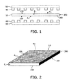
- FIG. 1 shows a schematic cross-sectional partial view of a light-emitting device according to a first embodiment.
- FIG. 2 shows a perspective view of the conversion structure of the light emitting device of FIG. 1 .
- FIG. 3 shows a—very schematic—top view of several LEDs of a light emitting device according to a second embodiment of the invention.
- FIG. 4 shows a perspective view of the conversion structure of a light emitting device according to a third embodiment.
- FIG. 5 is a graph showing the emission spectrum of a light emitting device and a LED used in the light emitting device according to Example 1.
- FIGS. 6A-6D illustrate example exit surface structures.
- FIG. 1 shows a schematic cross-sectional partial view of a light-emitting device 1 according to a first embodiment.
- the conversion structure 10 has a layer-like structure resembling a cuboid. It comprises two entrance surfaces, 100 and 110 (which cannot be seen in FIG. 1 due to the perspective) and one exit surface 200 .
- the surface area of the two entrance surfaces would be A 1 and A 2 , respectively, resulting in A being A 1 +A 2 .
- the ratio of A:E is set to be ⁇ 10:1 and ⁇ 10000:1; in this example A:E would be approximately 30:1.
- the embodiment in FIG. 1 is highly schematic and the ratio may be different for other applications.
- Further surfaces 300 are provided with a mirror, which cannot be seen in the FIG. 1 either.
- several LEDs 40 are provided, which emit light into the entrance surface.
- the LED may be provided on further parts, which are not part of this invention (indicated by the dotted lines and referred to by 50 and 60 ).
- FIG. 2 shows a perspective view of the conversion structure 10 of the light emitting device of FIG. 1 .
- the further surfaces 300 are provided with a mirror 300 ′.
- the at least one entrance surface has a roughness Ra of ⁇ 1 nm and ⁇ 500 nm, preferably ⁇ 10 nm and ⁇ 100 nm and more preferably ⁇ 20 nm and ⁇ 40 nm.
- the embodiment of the present system shown in the figures according to the present invention may be used in a broad variety of systems and/or applications, including one or more of the following: household application systems, shop lighting systems, home lighting systems, accent lighting systems, spot lighting systems, theater lighting systems, fiber-optics application systems, projection systems, self-lit display systems, pixelated display systems, segmented display systems, warning sign systems, medical lighting application systems, indicator sign systems, decorative lighting systems, portable systems and automotive applications.
- FIG. 3 shows a—very schematic—top view of several LEDs 40 ′ of a light emitting device according to a second embodiment of the invention.
- the further parts on which the LEDs may be mounted and/or provided have been omitted.
- the corresponding entrance surface 100 ′ of the conversion structure 10 ′ is shown.
- the LEDs 40 ′ may be provided in a grid-like structure with enough room between them in order to avoid that the LEDs may get too hot.
- the LEDs 40 ′ are mounted with a packing density ⁇ 0.05 and ⁇ 0.5.
- FIG. 4 shows a perspective view of the conversion structure 10 ′′ with an entrance surface 100 ′′ and an exit surface 200 ′′ according to a third embodiment of the invention.
- the conversion structure may be set to be a different shape than a cuboid, with the entrance surface having somewhat the shape of a trapezoid. By doing so, the light flux may be even enhanced, which may be advantageous for some applications.
- the lighting device according to the invention is—in a merely exemplary embodiment—furthermore illustrated by the following example:
- the ceramic precursor powder is then milled with 2 mm alumina balls in ethanol for 4 hrs, dried and granulated with PVA binder.
- Ceramic green bodies are formed by cold uniaxial pressing (3.2 kbar). Firing is done by sinter-HIP at 1750° C. (2 hrs pressureless sintering+10 hrs sintering in argon at 1 kbar). Out of this starting material, a conversion structure with a “box-like”-shape having dimensions of 4 ⁇ 30 ⁇ 1 mm 3 is formed, the index of refraction of the conversion structure being approx. 1.8.
- the conversion structure was then shaped and provided as described above in such a way that both 4 ⁇ 30 mm 2 surfaces were designed as entrance surfaces, whereas one 4 ⁇ 1 mm 2 surface was designed as an exit surface.
- the conversion structure was then post-annealed at 1250° C. for 12 hrs in air.
- the conversion structure was then mounted in a 5 ⁇ 35 ⁇ 8 mm 3 box with one 5 ⁇ 8 mm 2 side open. Both 5 ⁇ 35 mm 2 sides carry 20 1 mm 2 blue emitting LEDs, connected in parallel and in series to an appropriate external power supply. With the LEDs operated together at 40 W electrical power input, the lumen flux at the exit surface of the ceramic is 15 MCd/m 2 at a total flux of 350 lumen.
- FIG. 5 shows the emission spectra of a light emitting device which was made according to the example, and an emission spectrum of one of the employed LEDs. It can be seen that a very broad spectrum over the desired wavelength area can be reached, although the different LEDs have only a small emission spectrum covering less than 100 nm with a maximum around 450 nm.
Landscapes
- Physics & Mathematics (AREA)
- Optics & Photonics (AREA)
- General Physics & Mathematics (AREA)
- Engineering & Computer Science (AREA)
- Microelectronics & Electronic Packaging (AREA)
- General Engineering & Computer Science (AREA)
- Led Device Packages (AREA)
- Luminescent Compositions (AREA)
- Non-Portable Lighting Devices Or Systems Thereof (AREA)
Applications Claiming Priority (4)
| Application Number | Priority Date | Filing Date | Title |
|---|---|---|---|
| EP04105908.0 | 2004-11-18 | ||
| EP04105908 | 2004-11-18 | ||
| EP04105908 | 2004-11-18 | ||
| PCT/IB2005/053683 WO2006054203A1 (en) | 2004-11-18 | 2005-11-09 | Light emitting device with conversion structure |
Publications (2)
| Publication Number | Publication Date |
|---|---|
| US20090078949A1 US20090078949A1 (en) | 2009-03-26 |
| US7982229B2 true US7982229B2 (en) | 2011-07-19 |
Family
ID=35781207
Family Applications (1)
| Application Number | Title | Priority Date | Filing Date |
|---|---|---|---|
| US11/719,244 Active 2027-08-03 US7982229B2 (en) | 2004-11-18 | 2005-11-09 | Light emitting device with conversion structure |
Country Status (8)
| Country | Link |
|---|---|
| US (1) | US7982229B2 (zh) |
| EP (1) | EP1815532B1 (zh) |
| JP (1) | JP2008521233A (zh) |
| CN (1) | CN100472827C (zh) |
| AT (1) | ATE398836T1 (zh) |
| DE (1) | DE602005007629D1 (zh) |
| TW (1) | TWI400816B (zh) |
| WO (1) | WO2006054203A1 (zh) |
Cited By (16)
| Publication number | Priority date | Publication date | Assignee | Title |
|---|---|---|---|---|
| US20130146930A1 (en) * | 2010-11-30 | 2013-06-13 | Panasonic Corporation | Phosphor and light emitting device |
| WO2014155227A1 (en) | 2013-03-29 | 2014-10-02 | Koninklijke Philips N.V. | Light emitting device comprising wavelength converter |
| WO2014155250A1 (en) | 2013-03-29 | 2014-10-02 | Koninklijke Philips N.V. | Light emitting device comprising wavelength converter |
| WO2015185469A1 (en) * | 2014-06-05 | 2015-12-10 | Koninklijke Philips N.V. | Luminescence concentrator with increased efficiency |
| US20160315232A1 (en) * | 2014-01-02 | 2016-10-27 | Philips Lighting Holding B.V. | Light emitting device comprising releasable wavelength converter |
| WO2017054937A1 (en) | 2015-09-29 | 2017-04-06 | Philips Lighting Holding B.V. | Light source with diffractive outcoupling |
| US20170329065A1 (en) * | 2014-10-21 | 2017-11-16 | Imperial Innovations Limited | A Light Source |
| US9921353B2 (en) | 2013-06-14 | 2018-03-20 | Philips Lighting Holding B.V. | Light emitting device |
| WO2018083351A1 (en) | 2016-11-07 | 2018-05-11 | Koninklijke Philips N.V. | Device and method for physiological parameter detection |
| US10261402B2 (en) | 2017-03-29 | 2019-04-16 | Seiko Epson Corporation | Light source device and projector |
| US10379284B2 (en) | 2017-03-29 | 2019-08-13 | Seiko Epson Corporation | Light source device and projector |
| US10746931B2 (en) | 2018-07-27 | 2020-08-18 | Seiko Epson Corporation | Light source device and projector |
| US10969529B2 (en) * | 2015-10-20 | 2021-04-06 | Signify Holding B.V. | Spot lighting device having light guide with plurality of light converting segments |
| US11067734B2 (en) * | 2018-11-18 | 2021-07-20 | Juganu Ltd. | Illumination device having a plurality of different colored LEDs coupled to a solid waveguide |
| WO2022064168A1 (en) | 2020-09-25 | 2022-03-31 | Coolled Limited | Spectral output homogenising apparatus |
| US11604321B2 (en) | 2018-12-04 | 2023-03-14 | Signify Holding B.V. | Light generating system comprising an elongated luminescent body |
Families Citing this family (60)
| Publication number | Priority date | Publication date | Assignee | Title |
|---|---|---|---|---|
| US8684555B2 (en) | 2006-04-26 | 2014-04-01 | Koninklijke Philips N.V. | Light emitting device with ceramic conversion material |
| WO2008056296A1 (en) * | 2006-11-06 | 2008-05-15 | Koninklijke Philips Electronics N.V. | Wavelength converting elements with reflective edges |
| US10788678B2 (en) | 2013-05-17 | 2020-09-29 | Excelitas Canada, Inc. | High brightness solid state illumination system for fluorescence imaging and analysis |
| WO2015007755A2 (en) * | 2013-07-19 | 2015-01-22 | Koninklijke Philips N.V. | A light emitting device and a method for dimming a light emitting device |
| US9810826B2 (en) | 2014-01-28 | 2017-11-07 | Philips Lighting Holding B.V. | Light emitting device |
| EP2947484B1 (en) * | 2014-05-14 | 2017-04-05 | Philips Lighting Holding B.V. | A light emitting device |
| DE102014107345A1 (de) * | 2014-05-26 | 2015-11-26 | Hella Kgaa Hueck & Co. | Beleuchtungsvorrichtung für Fahrzeuge |
| EP3224674B1 (en) * | 2014-11-11 | 2021-04-14 | Lumileds LLC | Lighting device with ceramic garnet |
| KR102432725B1 (ko) * | 2015-02-23 | 2022-08-17 | 코닌클리케 필립스 엔.브이. | 안정적인 유속 출력 대 온도를 갖는 백색 인광체 변환 led |
| EP3292739B1 (en) * | 2015-05-07 | 2020-02-19 | Signify Holding B.V. | High intensity light source with temperature independent color point |
| JP6427718B2 (ja) * | 2015-09-29 | 2018-11-21 | フィリップス ライティング ホールディング ビー ヴィ | セラミックガーネットを備える照明デバイス |
| JP6427721B1 (ja) | 2015-12-11 | 2018-11-21 | フィリップス ライティング ホールディング ビー ヴィ | 積層ルミネッセンス集光器 |
| EP3390901B1 (en) * | 2015-12-15 | 2019-09-11 | Signify Holding B.V. | Multiple pumping luminescent rod configuration for obtaining ultra-high brightness |
| EP3430308A1 (en) | 2016-03-15 | 2019-01-23 | Philips Lighting Holding B.V. | Compound parabolic collimator array for high intensity lighting |
| WO2018141625A1 (en) | 2017-02-03 | 2018-08-09 | Philips Lighting Holding B.V. | Light concentrator module |
| EP3583347A1 (en) | 2017-02-17 | 2019-12-25 | Signify Holding B.V. | Light concentrator module |
| US10976479B2 (en) | 2017-03-28 | 2021-04-13 | Signify Holding B.V. | Light concentrator module with high refractive index interconnect |
| EP3625604B1 (en) | 2017-05-16 | 2021-01-20 | Signify Holding B.V. | Color mixing in laser-based light source |
| EP3649398A1 (en) | 2017-07-07 | 2020-05-13 | Signify Holding B.V. | Light concentrator module |
| WO2019008073A1 (en) | 2017-07-07 | 2019-01-10 | Philips Lighting Holding B.V. | LIGHTING DEVICE |
| JP6818168B2 (ja) | 2017-07-07 | 2021-01-20 | シグニファイ ホールディング ビー ヴィSignify Holding B.V. | 集光器モジュール |
| WO2019008092A1 (en) | 2017-07-07 | 2019-01-10 | Philips Lighting Holding B.V. | CONCENTRATING MODULE OF LIGHT |
| WO2019016006A1 (en) | 2017-07-18 | 2019-01-24 | Philips Lighting Holding B.V. | LIGHT ENGINE WITH HIGH PIXELIZED BRIGHTNESS |
| JP7090842B2 (ja) * | 2017-07-27 | 2022-06-27 | 日本電気硝子株式会社 | 波長変換部材及び発光装置 |
| EP3685099B1 (en) | 2017-09-21 | 2022-07-13 | Signify Holding B.V. | Luminescent concentrator with cpc, light guide and additional phosphor |
| US11356645B2 (en) | 2017-10-19 | 2022-06-07 | Signify Holding B.V. | Enhanced white light for projection lighting |
| JP7344202B2 (ja) | 2017-11-14 | 2023-09-13 | シグニファイ ホールディング ビー ヴィ | カラーホイールと共に使用される場合にデジタルスポークを可能にする固体光源 |
| US11079530B2 (en) | 2018-03-29 | 2021-08-03 | Signify Holding B.V. | Lighting system with light guiding body having trivalent cerium luminescent material |
| CN108410451B (zh) * | 2018-04-12 | 2020-07-31 | 山东大学 | 一种尖晶石基颜色可调控的上转换发光材料及其制备方法和应用 |
| WO2019233876A1 (en) | 2018-06-05 | 2019-12-12 | Signify Holding B.V. | Light concentrator module |
| JP6874743B2 (ja) | 2018-07-20 | 2021-05-19 | セイコーエプソン株式会社 | 光源装置およびプロジェクター |
| JP2020016856A (ja) | 2018-07-27 | 2020-01-30 | セイコーエプソン株式会社 | 光源装置およびプロジェクター |
| JP7040345B2 (ja) | 2018-07-30 | 2022-03-23 | セイコーエプソン株式会社 | 光源装置およびプロジェクター |
| US11537036B2 (en) | 2018-08-10 | 2022-12-27 | Sony Corporation | Light source apparatus and projector |
| TWI676851B (zh) | 2018-08-22 | 2019-11-11 | 隆達電子股份有限公司 | 畫素陣列封裝結構及顯示面板 |
| JP7238294B2 (ja) | 2018-08-24 | 2023-03-14 | セイコーエプソン株式会社 | 光源装置およびプロジェクター |
| CN110865504B (zh) | 2018-08-27 | 2021-08-17 | 精工爱普生株式会社 | 光源装置和投影仪 |
| JP2020042133A (ja) | 2018-09-10 | 2020-03-19 | セイコーエプソン株式会社 | 光源装置およびプロジェクター |
| WO2020078790A1 (en) | 2018-10-16 | 2020-04-23 | Signify Holding B.V. | Hld module with improved thermal performance |
| WO2020089246A1 (en) | 2018-11-01 | 2020-05-07 | Signify Holding B.V. | Lcd engine architecture |
| JP6881423B2 (ja) | 2018-11-22 | 2021-06-02 | セイコーエプソン株式会社 | 光源装置およびプロジェクター |
| US11215747B2 (en) * | 2018-11-30 | 2022-01-04 | Seiko Epson Corporation | Light source device and electronic apparatus |
| JP6888637B2 (ja) * | 2019-01-10 | 2021-06-16 | セイコーエプソン株式会社 | 光源装置、プロジェクター及び蛍光体ロッド |
| WO2020254439A1 (en) | 2019-06-21 | 2020-12-24 | Signify Holding B.V. | Hld module with cavity for improved light coupling |
| WO2020254455A1 (en) | 2019-06-21 | 2020-12-24 | Signify Holding B.V. | Hld module with improved cooling of a luminescent body |
| US11933490B2 (en) * | 2019-07-15 | 2024-03-19 | Signify Holding, B.V. | Laser phosphor based light source with improved brightness |
| WO2021028426A1 (en) | 2019-08-13 | 2021-02-18 | Signify Holding B.V. | Adjustable ratio of converted to transmitted light in transparent luminescent converter |
| EP4018122B1 (en) | 2019-08-20 | 2024-02-14 | Signify Holding B.V. | High intensity light source with high cri |
| JP7142188B1 (ja) | 2019-09-18 | 2022-09-26 | シグニファイ ホールディング ビー ヴィ | 高いcriの高強度光源 |
| WO2021063878A1 (en) | 2019-10-01 | 2021-04-08 | Signify Holding B.V. | High-intensity color tunable white laser light source using green phosphor |
| WO2021069562A1 (en) | 2019-10-10 | 2021-04-15 | Signify Holding B.V. | White luminescent concentrator with ld coupling as additional channel |
| JP7274050B2 (ja) | 2019-10-22 | 2023-05-15 | シグニファイ ホールディング ビー ヴィ | 高強度レーザポンピング光源に関する熱管理及び効率の改善 |
| CN114641648A (zh) | 2019-10-29 | 2022-06-17 | 昕诺飞控股有限公司 | 具有高cri和r9的高强度光源 |
| EP4111095B1 (en) | 2020-02-27 | 2023-11-15 | Signify Holding B.V. | Light generating device with a beam shaping optical element |
| US11347141B2 (en) | 2020-03-23 | 2022-05-31 | Seiko Epson Corporation | Light source device and projector |
| JP7127662B2 (ja) | 2020-03-26 | 2022-08-30 | セイコーエプソン株式会社 | 光源装置およびプロジェクター |
| WO2021219442A1 (en) | 2020-04-30 | 2021-11-04 | Signify Holding B.V. | High intensity light source with high cri for low ctt using green laser pumped phosphor |
| US11927342B2 (en) | 2020-06-16 | 2024-03-12 | Signify Holding B.V. | High-intensity light source with high CRI |
| WO2022096271A1 (en) | 2020-11-03 | 2022-05-12 | Signify Holding B.V. | Laser phosphor lighting device providing beam shaping using concentric fibers |
| EP4109527A1 (en) * | 2021-06-25 | 2022-12-28 | Centre national de la recherche scientifique | Light emitting device comprising a cooling system |
Citations (11)
| Publication number | Priority date | Publication date | Assignee | Title |
|---|---|---|---|---|
| JPH07176794A (ja) | 1993-12-17 | 1995-07-14 | Nichia Chem Ind Ltd | 面状光源 |
| US5590147A (en) * | 1994-12-19 | 1996-12-31 | The Morgan Curcible Company Plc | Side-pumped lasers |
| WO1998012757A1 (de) | 1996-09-20 | 1998-03-26 | Siemens Aktiengesellschaft | Wellenlängenkonvertierende vergussmasse, deren verwendung und verfahren zu deren herstellung |
| US5982092A (en) | 1997-10-06 | 1999-11-09 | Chen; Hsing | Light Emitting Diode planar light source with blue light or ultraviolet ray-emitting luminescent crystal with optional UV filter |
| EP1139440A2 (en) | 2000-03-27 | 2001-10-04 | General Electric Company | White light illumination system with improved color output |
| US20010036083A1 (en) | 1999-01-29 | 2001-11-01 | Weber Andreas G. | Green phosphor converted light emitting diode |
| US20020080501A1 (en) * | 2000-06-20 | 2002-06-27 | Hiroyuki Kawae | Light permeable fluorescent cover for light emitting diode |
| US20020113244A1 (en) | 2001-02-22 | 2002-08-22 | Barnett Thomas J. | High power LED |
| WO2004021460A2 (en) | 2002-08-30 | 2004-03-11 | Gelcore Llc | Light emitting diode planar light source and low-profile headlight constructed therewith |
| EP1418629A2 (en) | 2002-11-06 | 2004-05-12 | Koito Manufacturing Co., Ltd. | Vehicular headlamp using semiconductor light-emitting elements and manufacturing method thereof |
| US20040145308A1 (en) | 2002-10-22 | 2004-07-29 | Osram Opto Semiconductors Gmbh | Light source having an LED and a luminescence conversion body and method for producing the luminescence conversion body |
Family Cites Families (6)
| Publication number | Priority date | Publication date | Assignee | Title |
|---|---|---|---|---|
| US6404127B2 (en) * | 1993-07-20 | 2002-06-11 | University Of Georgia Research Foundation, Inc. | Multi-color microcavity resonant display |
| JP2001517875A (ja) * | 1997-09-25 | 2001-10-09 | ユニバーシティ オブ ブリストル | 光照射装置 |
| JP3421621B2 (ja) * | 1999-12-24 | 2003-06-30 | 三洋電機株式会社 | 面光源装置 |
| DE10026435A1 (de) * | 2000-05-29 | 2002-04-18 | Osram Opto Semiconductors Gmbh | Kalzium-Magnesium-Chlorosilikat-Leuchtstoff und seine Anwendung bei Lumineszenz-Konversions-LED |
| JP2001343531A (ja) * | 2000-05-30 | 2001-12-14 | Canon Inc | 照明装置、この照明装置を有するイメージセンサーおよびこのイメージセンサーを用いた画像読取装置ならびに情報処理システム |
| JP3930900B2 (ja) * | 2002-12-27 | 2007-06-13 | 株式会社林創研 | 照明装置 |
-
2005
- 2005-11-09 WO PCT/IB2005/053683 patent/WO2006054203A1/en active IP Right Grant
- 2005-11-09 AT AT05803070T patent/ATE398836T1/de not_active IP Right Cessation
- 2005-11-09 JP JP2007542384A patent/JP2008521233A/ja active Pending
- 2005-11-09 US US11/719,244 patent/US7982229B2/en active Active
- 2005-11-09 CN CNB2005800395823A patent/CN100472827C/zh active Active
- 2005-11-09 EP EP05803070A patent/EP1815532B1/en active Active
- 2005-11-09 DE DE602005007629T patent/DE602005007629D1/de active Active
- 2005-11-15 TW TW094140111A patent/TWI400816B/zh active
Patent Citations (11)
| Publication number | Priority date | Publication date | Assignee | Title |
|---|---|---|---|---|
| JPH07176794A (ja) | 1993-12-17 | 1995-07-14 | Nichia Chem Ind Ltd | 面状光源 |
| US5590147A (en) * | 1994-12-19 | 1996-12-31 | The Morgan Curcible Company Plc | Side-pumped lasers |
| WO1998012757A1 (de) | 1996-09-20 | 1998-03-26 | Siemens Aktiengesellschaft | Wellenlängenkonvertierende vergussmasse, deren verwendung und verfahren zu deren herstellung |
| US5982092A (en) | 1997-10-06 | 1999-11-09 | Chen; Hsing | Light Emitting Diode planar light source with blue light or ultraviolet ray-emitting luminescent crystal with optional UV filter |
| US20010036083A1 (en) | 1999-01-29 | 2001-11-01 | Weber Andreas G. | Green phosphor converted light emitting diode |
| EP1139440A2 (en) | 2000-03-27 | 2001-10-04 | General Electric Company | White light illumination system with improved color output |
| US20020080501A1 (en) * | 2000-06-20 | 2002-06-27 | Hiroyuki Kawae | Light permeable fluorescent cover for light emitting diode |
| US20020113244A1 (en) | 2001-02-22 | 2002-08-22 | Barnett Thomas J. | High power LED |
| WO2004021460A2 (en) | 2002-08-30 | 2004-03-11 | Gelcore Llc | Light emitting diode planar light source and low-profile headlight constructed therewith |
| US20040145308A1 (en) | 2002-10-22 | 2004-07-29 | Osram Opto Semiconductors Gmbh | Light source having an LED and a luminescence conversion body and method for producing the luminescence conversion body |
| EP1418629A2 (en) | 2002-11-06 | 2004-05-12 | Koito Manufacturing Co., Ltd. | Vehicular headlamp using semiconductor light-emitting elements and manufacturing method thereof |
Cited By (25)
| Publication number | Priority date | Publication date | Assignee | Title |
|---|---|---|---|---|
| US8816377B2 (en) * | 2010-11-30 | 2014-08-26 | Panasonic Corporation | Phosphor and light emitting device |
| US20130146930A1 (en) * | 2010-11-30 | 2013-06-13 | Panasonic Corporation | Phosphor and light emitting device |
| WO2014155227A1 (en) | 2013-03-29 | 2014-10-02 | Koninklijke Philips N.V. | Light emitting device comprising wavelength converter |
| WO2014155250A1 (en) | 2013-03-29 | 2014-10-02 | Koninklijke Philips N.V. | Light emitting device comprising wavelength converter |
| US9921353B2 (en) | 2013-06-14 | 2018-03-20 | Philips Lighting Holding B.V. | Light emitting device |
| US20160315232A1 (en) * | 2014-01-02 | 2016-10-27 | Philips Lighting Holding B.V. | Light emitting device comprising releasable wavelength converter |
| US9722152B2 (en) * | 2014-01-02 | 2017-08-01 | Philips Lighting Holding B.V. | Light emitting device comprising releasable wavelength converter |
| WO2015185469A1 (en) * | 2014-06-05 | 2015-12-10 | Koninklijke Philips N.V. | Luminescence concentrator with increased efficiency |
| US20170139113A1 (en) * | 2014-06-05 | 2017-05-18 | Philips Lighting Holding B.V. | Luminescence concentrator with increased efficiency |
| US10422942B2 (en) * | 2014-06-05 | 2019-09-24 | Signify Holding B.V. | Luminescence concentrator |
| US20170329065A1 (en) * | 2014-10-21 | 2017-11-16 | Imperial Innovations Limited | A Light Source |
| US10502882B2 (en) * | 2014-10-21 | 2019-12-10 | Imperial Innovations Limited | Light source |
| WO2017054937A1 (en) | 2015-09-29 | 2017-04-06 | Philips Lighting Holding B.V. | Light source with diffractive outcoupling |
| US10539730B2 (en) | 2015-09-29 | 2020-01-21 | Signify Holding B.V. | Light source with diffractive outcoupling |
| US10969529B2 (en) * | 2015-10-20 | 2021-04-06 | Signify Holding B.V. | Spot lighting device having light guide with plurality of light converting segments |
| WO2018083351A1 (en) | 2016-11-07 | 2018-05-11 | Koninklijke Philips N.V. | Device and method for physiological parameter detection |
| US11482034B2 (en) | 2016-11-07 | 2022-10-25 | Koninklijke Philips N.V. | Device and method for physiological parameter detection |
| US10379284B2 (en) | 2017-03-29 | 2019-08-13 | Seiko Epson Corporation | Light source device and projector |
| US10261402B2 (en) | 2017-03-29 | 2019-04-16 | Seiko Epson Corporation | Light source device and projector |
| US10746931B2 (en) | 2018-07-27 | 2020-08-18 | Seiko Epson Corporation | Light source device and projector |
| US11067734B2 (en) * | 2018-11-18 | 2021-07-20 | Juganu Ltd. | Illumination device having a plurality of different colored LEDs coupled to a solid waveguide |
| US11397291B2 (en) * | 2018-11-18 | 2022-07-26 | Juganu Ltd. | Illumination device having a plurality of different colored LEDs coupled to solid wedge-shaped waveguides |
| US11604321B2 (en) | 2018-12-04 | 2023-03-14 | Signify Holding B.V. | Light generating system comprising an elongated luminescent body |
| WO2022064168A1 (en) | 2020-09-25 | 2022-03-31 | Coolled Limited | Spectral output homogenising apparatus |
| DE112021005017T5 (de) | 2020-09-25 | 2023-07-27 | Coolled Limited | Apparat zum homogenisieren einer spektralausgabe |
Also Published As
| Publication number | Publication date |
|---|---|
| ATE398836T1 (de) | 2008-07-15 |
| WO2006054203A1 (en) | 2006-05-26 |
| CN100472827C (zh) | 2009-03-25 |
| EP1815532B1 (en) | 2008-06-18 |
| DE602005007629D1 (de) | 2008-07-31 |
| JP2008521233A (ja) | 2008-06-19 |
| TW200631202A (en) | 2006-09-01 |
| US20090078949A1 (en) | 2009-03-26 |
| EP1815532A1 (en) | 2007-08-08 |
| CN101061591A (zh) | 2007-10-24 |
| TWI400816B (zh) | 2013-07-01 |
Similar Documents
| Publication | Publication Date | Title |
|---|---|---|
| US7982229B2 (en) | Light emitting device with conversion structure | |
| EP3047527B1 (en) | A light emitting device | |
| TWI414585B (zh) | 螢光體、製備及使用其之方法、發光裝置封裝件、表面光源設備及使用紅色螢光體之發光設備 | |
| US20090154137A1 (en) | Illumination Device Including Collimating Optics | |
| EP2803898B1 (en) | A light-emitting apparatus | |
| TWI420054B (zh) | 具有波長轉換元件之側持式散熱器的照明裝置 | |
| KR101460484B1 (ko) | 다수 컬러형 광-방출 공급원 및 확산기 부재를 이용한 조명 시스템 | |
| EP3071876B1 (en) | Light emitting device with spectral conversion element | |
| CN110945285B (zh) | 照明设备和照明系统 | |
| EP3987223B1 (en) | Hld module with cavity for improved light coupling | |
| JP2020534658A (ja) | Cpc、光ガイド、及び追加的蛍光体を有するルミネッセンス集光器 | |
| EP4103997B1 (en) | Compact laser-based light generating device | |
| EP3221637B1 (en) | A light emitting device | |
| US20230408802A1 (en) | Laser smd package with phosphor and light incoupler | |
| EP4111095B1 (en) | Light generating device with a beam shaping optical element | |
| CN2840331Y (zh) | 白光发光装置 | |
| JP7322318B2 (ja) | レーザ蛍光体ベースの画素化光源 | |
| CN112005049B (zh) | 高流明密度灯的单面照明 | |
| EP4048942B1 (en) | Improved heat management and efficiency for high intensity laser pumped light source | |
| CN117480343A (zh) | 使用锥形光纤改善热管理的基于激光器的光引擎 | |
| CN117242158A (zh) | 包括泵浦绿色/黄色磷光体的蓝色激光器和泵浦红色磷光体的黄色/橙色超发光二极管的高亮度光源 |
Legal Events
| Date | Code | Title | Description |
|---|---|---|---|
| AS | Assignment |
Owner name: KONINKLIJKE PHILIPS ELECTRONICS N V, NETHERLANDS Free format text: ASSIGNMENT OF ASSIGNORS INTEREST;ASSIGNORS:BECHTEL, HANS-HELMUT;BUSSELT, WOLFGANG;GOLSCH, SILVIA;AND OTHERS;REEL/FRAME:019288/0531;SIGNING DATES FROM 20060425 TO 20060428 Owner name: KONINKLIJKE PHILIPS ELECTRONICS N V, NETHERLANDS Free format text: ASSIGNMENT OF ASSIGNORS INTEREST;ASSIGNORS:BECHTEL, HANS-HELMUT;BUSSELT, WOLFGANG;GOLSCH, SILVIA;AND OTHERS;SIGNING DATES FROM 20060425 TO 20060428;REEL/FRAME:019288/0531 |
|
| STCF | Information on status: patent grant |
Free format text: PATENTED CASE |
|
| FPAY | Fee payment |
Year of fee payment: 4 |
|
| AS | Assignment |
Owner name: KONINKLIJKE PHILIPS N.V., NETHERLANDS Free format text: CHANGE OF NAME;ASSIGNOR:KONINKLIJKE PHILIPS ELECTRONICS N.V.;REEL/FRAME:039428/0606 Effective date: 20130515 |
|
| AS | Assignment |
Owner name: PHILIPS LIGHTING HOLDING B.V., NETHERLANDS Free format text: ASSIGNMENT OF ASSIGNORS INTEREST;ASSIGNOR:KONINKLIJKE PHILIPS N.V.;REEL/FRAME:040060/0009 Effective date: 20160607 |
|
| CC | Certificate of correction | ||
| MAFP | Maintenance fee payment |
Free format text: PAYMENT OF MAINTENANCE FEE, 8TH YEAR, LARGE ENTITY (ORIGINAL EVENT CODE: M1552); ENTITY STATUS OF PATENT OWNER: LARGE ENTITY Year of fee payment: 8 |
|
| AS | Assignment |
Owner name: SIGNIFY HOLDING B.V., NETHERLANDS Free format text: CHANGE OF NAME;ASSIGNOR:PHILIPS LIGHTING HOLDING B.V.;REEL/FRAME:050837/0576 Effective date: 20190201 |
|
| MAFP | Maintenance fee payment |
Free format text: PAYMENT OF MAINTENANCE FEE, 12TH YEAR, LARGE ENTITY (ORIGINAL EVENT CODE: M1553); ENTITY STATUS OF PATENT OWNER: LARGE ENTITY Year of fee payment: 12 |
|
| AS | Assignment |
Owner name: LUMENCOR, INC., OREGON Free format text: ASSIGNMENT OF ASSIGNORS INTEREST;ASSIGNOR:SIGNIFY HOLDING B.V.;REEL/FRAME:066422/0021 Effective date: 20231117 |