US7944200B2 - Probe apparatus - Google Patents
Probe apparatus Download PDFInfo
- Publication number
- US7944200B2 US7944200B2 US12/564,381 US56438109A US7944200B2 US 7944200 B2 US7944200 B2 US 7944200B2 US 56438109 A US56438109 A US 56438109A US 7944200 B2 US7944200 B2 US 7944200B2
- Authority
- US
- United States
- Prior art keywords
- test head
- probe card
- cam followers
- probe
- annular member
- Prior art date
- Legal status (The legal status is an assumption and is not a legal conclusion. Google has not performed a legal analysis and makes no representation as to the accuracy of the status listed.)
- Expired - Fee Related, expires
Links
Images


Classifications
-
- G—PHYSICS
- G01—MEASURING; TESTING
- G01R—MEASURING ELECTRIC VARIABLES; MEASURING MAGNETIC VARIABLES
- G01R31/00—Arrangements for testing electric properties; Arrangements for locating electric faults; Arrangements for electrical testing characterised by what is being tested not provided for elsewhere
- G01R31/28—Testing of electronic circuits, e.g. by signal tracer
- G01R31/2851—Testing of integrated circuits [IC]
- G01R31/2886—Features relating to contacting the IC under test, e.g. probe heads; chucks
- G01R31/2887—Features relating to contacting the IC under test, e.g. probe heads; chucks involving moving the probe head or the IC under test; docking stations
-
- G—PHYSICS
- G01—MEASURING; TESTING
- G01R—MEASURING ELECTRIC VARIABLES; MEASURING MAGNETIC VARIABLES
- G01R31/00—Arrangements for testing electric properties; Arrangements for locating electric faults; Arrangements for electrical testing characterised by what is being tested not provided for elsewhere
- G01R31/26—Testing of individual semiconductor devices
-
- G—PHYSICS
- G01—MEASURING; TESTING
- G01R—MEASURING ELECTRIC VARIABLES; MEASURING MAGNETIC VARIABLES
- G01R1/00—Details of instruments or arrangements of the types included in groups G01R5/00 - G01R13/00 and G01R31/00
- G01R1/02—General constructional details
- G01R1/06—Measuring leads; Measuring probes
-
- H—ELECTRICITY
- H10—SEMICONDUCTOR DEVICES; ELECTRIC SOLID-STATE DEVICES NOT OTHERWISE PROVIDED FOR
- H10P—GENERIC PROCESSES OR APPARATUS FOR THE MANUFACTURE OR TREATMENT OF DEVICES COVERED BY CLASS H10
- H10P74/00—Testing or measuring during manufacture or treatment of wafers, substrates or devices
Definitions
- the present invention relates to a probe apparatus which measures electric characteristics of a substrate by bringing probes into contact with electrode pads of the substrate; and more particularly, to a technique for mounting a test head to a ceiling plate of a main body of a probe apparatus.
- the quality of the device is determined by testing an electric characteristic of each integrated circuit chip of a wafer after the chips are completed.
- a test apparatus called a probe apparatus including: a main body in which a mounting table for mounting, e.g., a semiconductor wafer is provided; a probe card installed in a head plate (ceiling plate) of the main body and having probes provided at its bottom surface, the probes being brought into contact with electrode pads of a chip; and a box-shaped test head provided above the probe card and connected to the probe card via a pogo ring having pogo pins in its top and bottom surfaces.
- a pivot mechanism having a rotation shaft, which is rotatable about a horizontal axis, is provided at a side of the main body of the probe apparatus and the test head is supported at its side by an arm extending from the rotation shaft.
- the test head is pivotable from a horizontal position toward its back surface at an upper side of the probe apparatus.
- the probes of the probe card are arranged according to the electric pads of chips, it is required to exchange the probe card depending on kinds of wafers to be tested. Accordingly, there has been suggested a structure in which the probe card is held by a card holder and an elevation mechanism is provided to move the card holder upward and downward.
- the probe card is moved upward to press the pogo ring of the test head.
- the probe card is moved downward and separated from the pogo ring and then the probe card is drawn out from an outer side of the main body by sliding the card holder aside.
- the test head remains its horizontal posture. However, in the maintenance, the test head is pivoted and separated from the head plate. When the maintenance is finished, the test head returns to the horizontal posture.
- a regular load is required to make sure the electrical contact between the pogo ring and the probe card.
- To apply the load it is necessary to push the test head relatively downward (or to push the probe card relatively upward) by, e.g. about 2 mm after the test head is brought into contact with the probe card.
- the elevation mechanism is provided at the card holder to acquire the fine elevation amount.
- the above probe apparatus requires the mechanisms for sliding the card holder aside and moving the card holder upward and downward, which increases the cost of the probe apparatus.
- an operator may exchange the probe card to the upper surface of the head plate. In this case, since it is necessary to accurately move the card holder upward by a fine amount in a state where the card holder is mounted to the head plate, a complex elevation mechanism is needed.
- test apparatuses have been disclosed in, e.g., Japanese Patent Laid-open Applications Nos. H03-022546 and H02-177343. Further, e.g., Japanese Patent Laid-open Applications Nos. H01-272982 ( FIG. 1 ) and H10-050778 (FIG. 2 )), disclose mechanisms for accurately aligning the positions of the test head and the wafer or for horizontally holding the test head. However, any consideration related to the aforementioned issue is not reflected to the above patent documents.
- the present invention provides a probe apparatus that can simply, inexpensively test a substrate with high accuracy.
- a probe apparatus for testing electrical characteristics of a target chip of a substrate by bringing probes formed on a lower surface of a probe card into contact with electrical pads of the target chip, in which the probe card is mounted in an opening formed in a ceiling plate of a main body of the apparatus and a test head is arranged above the probe card, the apparatus comprising: a pivot mechanism for pivoting the test head, about its horizontal rotary shaft, between a horizontal position at which a lower surface of the test head is horizontally located above the probe card and a separated position at which the test head is separated from the ceiling plate of the main body; a holding frame connected to the rotary shaft and holding the test head through a biasing unit biasing the test head when the test head is horizontally located; a annular member rotatably mounted in a peripheral portion of the opening in its circumferential direction; cam followers provided at the annular member along its circumferential direction to be rotatable about their horizontal axes extending toward a rotational center
- FIG. 1 is a perspective view showing a probe apparatus in accordance with a first embodiment of the present invention
- FIG. 2 is a plan view showing the probe apparatus shown in FIG. 1 ;
- FIG. 3 is an enlarged perspective view showing a test head of the probe apparatus shown in FIG. 1 ;
- FIG. 4 is a vertically cross sectional view showing the probe apparatus shown in FIG. 1 ;
- FIG. 5 is an exploded perspective view showing the head plate, a slide ring and a pogo ring provided in a lower surface of the test head shown in FIG. 3 ;
- FIGS. 6A and 6B are schematic views showing the pogo ring and the slide ring shown in FIG. 5 ;
- FIG. 7 is an enlarged vertically cross sectional view showing the pogo ring shown in FIG. 5 ;
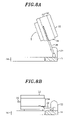
- FIGS. 8A and 8B show how the probe apparatus shown in FIG. 1 is operated
- FIG. 9 shows how the probe apparatus shown in FIG. 1 is operated
- FIGS. 10A to 10C show how the probe apparatus shown in FIG. 1 is operated
- FIGS. 11A and 11B show how the probe apparatus shown in FIG. 1 is operated
- FIGS. 12A and 12B show how the probe apparatus shown in FIG. 1 is operated
- FIGS. 13A to 13C show how the probe apparatus shown in FIG. 1 is operated
- FIG. 14 shows how the probe apparatus shown in FIG. 1 is operated
- FIG. 15 is a vertically cross sectional view showing a probe apparatus in accordance with a second embodiment of the present invention.
- FIG. 16 is a plan view showing the probe apparatus shown FIG. 15 ;
- FIG. 17 is an enlarged schematic view showing a pogo ring of the probe apparatus shown in FIG. 15 ;
- FIGS. 18A and 18B show how the probe apparatus shown in FIG. 15 is operated
- FIG. 19 is a vertically cross sectional view showing a probe apparatus in accordance with a third embodiment of the present invention.
- FIG. 20 is a plan view showing the probe apparatus shown in FIG. 19 ;
- FIGS. 21A and 21B are enlarged schematic views showing a pogo ring of the probe apparatus shown in FIG. 19 ;
- FIG. 22 is a vertically cross sectional view showing a probe apparatus in accordance with a fourth embodiment of the present invention.
- the probe apparatus includes a main body 11 , a test head 12 , and a loader unit 13 provided adjacent to the main body 11 .
- the arrangement direction of the main body 11 and the loader unit 13 is defined as a left-light direction and the lower and the upper side in FIG. 2 are defined as a front side and a back side, respectively.
- the main body 11 includes an exterior housing 20 .
- an opening 22 having, e.g., a rectangular shape is formed in a ceiling plate 21 of the housing 20 .
- a rectangular head plate 24 is provided to cover the opening 22 .
- a guide mechanism 23 extending front and back is formed at, e.g., a lower edge side such that the head plate 24 is mountable and detachable with respect to the main body 11 by sliding front and back.
- An upper surface of the head plate 24 is flush with an upper surface of the ceiling plate 21 .
- a front upper surface of the housing 20 is cut out in a rectangular shape to prevent the housing 20 from colliding with the head plate when the head plate 24 is mounted and detached.
- a central portion of the front upper surface of the housing 20 is further cut out in a lower direction to prevent interference with probe needles 27 , which will be described below.
- the head plate 24 When the head plate 24 is mounted to the main body 11 , the head plate 24 is fixably joined to the main body 11 by, e.g., volts (not shown) or the like.
- the head plate 24 is shown in FIG. 1 with a portion thereof cut out.
- a box-shaped test head 12 having a weight of, e.g., about 60 kg is provided above the head plate 24 .
- the test head 12 is held in its opposite sides by a holding frame 35 having an approximately C-shape (i.e., a rectangular shape with one side open).
- a hinge mechanism 32 which is a pivot mechanism, is provided at a left side of a back edge portion of the ceiling plate 21 (a left side of an X-direction in FIG. 1 ).
- a back side of the holding frame 35 is connected to a rotary shaft 31 of the hinge mechanism 32 via a plate-shaped rotation arm 33 . Accordingly, the holding frame 35 is rotated by the rotary shaft 31 .
- test head 12 is pivotable between an inclinedly separated position at which the test head 12 is pivoted upward and separated from the head plate 24 and a horizontal position at which the test head 12 is horizontally disposed to face the head plate 24 .
- a rotational center of the rotary shaft 31 is located at a position that is, e.g., about 140 mm higher than that of an upper surface of the ceiling plate 21 .
- Reinforcement plates 42 are attached to opposite side surfaces of the test head 12 .
- the test head 12 is held by the holding frame 35 through two pairs of gas springs 43 serving as biasing units, each pair of which is provided spaced apart from each other in the front-back direction between the reinforcement plate 42 and the arm 34 of the holding frame 35 .
- Each of the gas springs 43 extends in a thickness (vertical) direction of the test head 12 . Accordingly, when the test head 12 is horizontally located, upward restoration forces (biasing forces) of the gas springs 43 are balanced with the gravity of the test head 12 .
- test head 12 is horizontally pushed downward by, e.g., about 31 mm to a test position against the restoration forces of the gas springs 43 , which will be described below. For that reason, when the test head 12 is pivoted at, e.g., the upper position, there is a sufficient clearance between the test head 12 and the probe card 26 , a reinforcement member 28 , and other elements to prevent the test head 12 from interfering with them.
- Each of the opposite arms 34 includes a protrusion 34 a .
- the protrusion 34 a is formed by protruding a region of the arm 34 , located between the gas springs 43 in a longitudinal direction thereof toward the test head 12 in an approximate U-shape.
- Two guide rails 46 extending in the thickness direction of the test head 12 are provided at two positions in the reinforcement plate 42 facing the protrusion 34 a and guide members 45 are provided in the protrusions 34 a to guide the guide rails 46 , respectively. Accordingly, when the test head 12 is horizontally located, the test head 12 is moved downward against the restoration forces of the gas springs 43 while the guide rails 46 are guided by the guide members 45 .
- a handle 39 shown in FIG. 1 is for an operator to rotate the test head 12 . In other drawings, the handle 39 may be omitted.
- Through holes 47 a and 47 b are formed at corresponding positions of the opposite arms 34 and the reinforcement plate 42 attached to the opposite side surfaces of the test head 12 , respectively.
- a lock pin 48 which is supported by a reciprocating mechanism (not shown) arranged in the main body 11 , may pass through the through holes 47 a and 47 b , or may be removed from the through holes 47 a and 47 b as desired.
- the lock pin 48 passes through the through holes 47 a and 47 b to lock the test head such that the test head 12 may not be slid upward or downward. However, when the test head 12 horizontally moved upward and downward, the lock pin is moved back to release the lock of the test head 12 .
- FIG. 3 shows the arm 34 with a portion thereof cut out.
- a pressing unit 36 is provided between the main body 11 and each of the opposite arms 34 .
- the pressing unit 36 applies a biasing force to pivot the corresponding arm 34 upward.
- the pressing unit 36 includes a biasing rod 38 urged to extend by a gas spring.
- a base end portion of the biasing rod 38 is joined to a back portion of the main body 11 to be rotatable about a horizontal axis and a leading end portion of the biasing rod 38 is rotatably joined to a lower surface of a supporting member 37 provided on a lower surface of the arm 34 .
- a pogo ring 51 is provided at a lower surface of the test head 12 as an intermediate connecting member for electrically connecting the test head 12 to the probe card 26 provided to the head plate 24 .
- the pogo ring 51 includes a ring member 54 made of an insulating material, e.g., a resin material and a plurality of pogo pins 51 a protruding from a lower surface of the ring member 54 .
- the pogo pins 51 a are biased to protrude (toward the probe card 26 ) by springs or the like (not shown) provided at their base end portions (on the side of the test head 12 ).
- the pogo pins 51 a are arranged corresponding to electrodes formed on an upper surface of the probe card 26 . Moreover, lower ends of the pogo pins 51 a are spaced apart from the upper surface of the probe card 26 by, e.g., about 30 mm when the test head 12 is horizontally located after being pivoted.
- a protrusion 52 outwardly protruding from the peripheral surface in a circular arc shape, i.e., along the peripheral surface of the pogo ring 51 is provided at a plurality of positions, e.g., four positions at regular intervals in a circumferential direction.
- Each of the protrusions 52 is formed such that an angle between opposite ends of the protrusion 52 and the center of the pogo ring 51 is about 70° when viewed from the top.
- An upper surface is inclined in a taper shape such that the height thereof gets higher in, e.g., a clockwise direction and serves as a guideway 55 for guiding an inner cam follower 66 to be described below.
- the guideway 55 includes an inclined surface 56 and a horizontal surface 57 horizontally extending from a top of the inclined surface 56 in the clockwise direction.
- the vertical height of the top of the inclined surface 56 is, e.g., about 33 mm.
- the protrusion 52 cooperates with a slide ring 61 provided in the main body 11 to push downward the pogo ring 51 (the test head 12 ) from the horizontal position to the test position. Described below are structures of the slide ring 61 and the head plate 24 .
- an opening part 25 having, e.g., a circular shape is formed to accommodate the probe card 26 , the pogo ring 51 and the slide ring 61 .
- a lower periphery portion of the opening part 25 protrudes inwardly to form a flange portion 25 a .
- a card holder 29 is detachably joined to the flange portion 25 a .
- the card holder 29 holds the probe card 26 having a circular shape of a diameter, e.g., 440 mm therein.
- FIG. 4 shows that the card holder 29 (the probe card 26 ) is mounted on the flange portion 25 a
- FIG. 5 shows that the card holder 29 is detached from the flange portion 25 a.
- Probes e.g. probe needles 27 are, e.g., vertically extended from a lower surface of the probe card 26 . Leading ends of the probe needles 27 are protruded downwardly to be located lower than a lower surface of the head plate 24 . Each of the probe needles 27 may be of a transverse needle type.
- the probe needles 27 are schematically shown in FIGS. 4 and 7 .
- the reinforcement member 28 having a circular plate shape is provided concentrically with the probe card 26 on an upper surface of the probe card 26 , for example, to prevent deformation of the probe card 26 .
- the pogo ring 51 has an inner diameter slightly greater than an outer diameter of the reinforcement member 28 and an outer diameter slightly smaller than an outer diameter of the probe card 26 .
- the slide ring 61 is provided concentrically shape with the pogo ring 51 on the flange portion 25 a of the opening part 25 to accommodate the pogo ring 51 and the protrusion 52 therein.
- outer cam followers 63 are provided at, e.g., eight positions at regular intervals in a circumferential direction.
- the outer cam followers 63 are rollers that are rotatable about their horizontal axes extending toward the rotational central axis of the slide ring 61 .
- the outer cam followers 63 are fixably joined to the vertical wall by respective central shafts 63 a extending along the rotational center line of the outer cam follower 63 .
- the slide ring 61 is rotatable about its vertical axis by the outer cam follower 63 .
- a ring portion 61 a protrudes outwardly from an upper portion of the slide ring 61 and extends in a circumferential direction.
- the slide ring 61 is rotatably supported by bringing the outer cam follower 63 into contact with a lower surface of the ring portion 61 a .
- a fixed ring 61 b protrudes outwardly from a lower portion of the slide ring 61 and extends circumferentially similarly to the ring surface portion 61 a .
- the fixed ring 61 b makes in contact with a lower side of the outer cam follower 63 to prevent the test head 12 from being moved upward, by the biasing force, from the head plate 24 .
- the slide ring 61 has an upper/lower two-divided structure (not shown) including an upper member having the ring portion 61 a and a lower member having the fixed ring 61 b .
- the lower member of the slide ring 61 is accommodated in the opening part 24 and then the outer cam followers 63 are joined to the vertical wall of the opening part 25 .
- the upper member is accommodated in the opening part 25 .
- the lower member and the upper member are joined to each other by using, e.g., volts or the like.
- hook portions 65 extending from a lower side of the slide ring 61 to above the slide ring 61 are provided at regular intervals in a circumferential direction at, e.g., four positions in an inner periphery of the slide ring 61 to correspond to the protrusions 52 arranged at the intervals.
- the inner cam follower 66 is provided in an inner side of each of the hook portions 65 at a position that is higher than that of the upper surface of the slide ring 61 .
- the inner cam follower includes, e.g., a roller that is rotatable about a horizontal axis extending toward the rotational central axis of the slide ring 61 .
- the inner cam follower 66 is fixably joined to the hook portion 65 by a central shaft 66 a extending along the rotational center line of the inner cam follower 66 .
- An upper portion of the hook portion 65 is bent inwardly to serve as a protection member for, e.g., preventing an operator from making in contact with the inner cam follower 66 .
- a distance between the lower surface of the inner cam follower 66 and the upper surface of the probe card 26 is set to, e.g., about 37 mm.
- a height h of the hook portion 65 is set to, e.g., about 54 mm.
- Both of the cam followers 63 and 66 are identically installed to be rotatable about their horizontal axes. However, for the easy distinguishing, the cam followers are called the inner cam follower 66 and the outer cam follower 63 .
- An operating lever 60 i.e., a manipulation part protrudes from an outer periphery of one of the hook portions 65 and the slide ring 61 is rotated by manipulating the operating lever 60 .
- lower ends of the inclined surfaces 56 of the protrusions 52 are located lower than the lower surface of the inner cam follower 66 .
- the inner cam followers 66 are moved upward along the respective guideways 55 as the slide ring 61 is rotated, the inner cam followers 66 push downward the pogo ring 51 (the test head 12 ) against the biasing force to allow the test head 12 is to be at the test position.
- the protrusions 52 and the slide ring 61 are omitted in FIGS. 1 to 3 .
- a mounting table 71 and a moving mechanism 72 are provided in the housing 20 of the main body 11 .
- the mounting table 71 mounts thereon a substrate, e.g., a semiconductor wafer W, having a surface on which a plurality of target chips is arranged.
- the moving mechanism 72 moves the mounting table 71 in X, Y, and Z directions and rotates the mounting table 71 about its vertical axis.
- the moving mechanism 72 includes an X-direction moving unit 73 , a Y-direction moving unit 74 , and a Z-direction moving unit 75 .
- a camera (not shown) for photographing the prove needles 27 is provided in the Z-direction moving unit 75 .
- Another camera (not shown) for photographing a surface of a wafer W is horizontally and movably installed at an upper side of the housing 20 . The alignment is performed by using the cameras.
- the loader unit 13 is connected to the right side of the main body 11 .
- the loader unit 13 includes an exterior housing 81 .
- An inner space of the housing 81 is divided into an upper space 83 and a lower space 84 by a partition wall 82 .
- a mounting member 85 for mounting thereon a FOUP 2 i.e., a sealed transfer container in which, e.g., 25 wafers are accommodated.
- An opening 86 is formed at a portion of the housing 81 on the right side of the FOUP 2 and the FOUP 2 is transferred between a transfer unit (not shown) and the mounting member 85 through the opening 86 .
- a transfer arm 87 is provided at a front side area in the housing 81 .
- the transfer arm 87 is rotatable about its vertical axis, vertically movable, and horizontally extensible and contractible.
- the transfer arm 87 transfers a wafer W between the FOUP 2 in the upper space 83 and the mounting table 71 of the main body 11 through an opening 88 formed between the main body 11 and the loader unit 13 .
- a control device 5 e.g., a computer, is provided in the probe apparatus.
- the control device 5 includes a program storage unit and a data processing unit having a central processing unit (CPU) and a memory.
- the programs stored in the program storage unit includes various process groups for attaching and detaching the test head 12 with respect to the head plate 24 , performing the transfer of a wafer W, position alignment of a wafer W, and performing a test of a wafer W.
- the memory stores a moving process of the moving mechanism 72 or includes a region into which processing parameter values such as a moving amount and the like are input.
- the programs (including programs related to display and input manipulation of processing parameters) are stored in a storage unit 6 such as a computer storage medium, e.g., a flexible disk, a compact disk, a magneto-optical (MO) disk, a hard disk, or the like and installed in the control device 5 .
- a storage unit 6 such as a computer storage medium, e.g., a flexible disk, a compact disk, a magneto-optical (MO) disk, a hard disk, or the like and installed in the control device 5 .
- test head 12 was pivoted upward and then a process of exchanging the probe card 26 mounted in the opening part 25 was finished.
- an operator rotates the test head 12 from a separated position shown in FIG. 8A to a horizontal position shown in FIG. 8B in which the test head 12 is horizontally located while gripping the handle 39 .
- the protrusions 52 formed in the side peripheral surface of the pogo ring 51 are located in spaces between the adjacent inner cam followers 66 , respectively.
- the lower ends of the inclined surfaces 56 of the protrusions 52 are located lower than the lower surfaces of the inner cam followers 66 as shown in FIG. 9 .
- the pogo pins 51 a of the pogo ring 51 are brought into contact with the probe card 26 as shown in FIG. 12A . Then, if the operating lever 60 is rotated by about 70° from the position shown in FIG. 10A in the clockwise direction to allow the inner cam followers 66 to be bought into contact with the horizontal surfaces 57 of the guideways 55 of the protrusions 52 , respectively, the pogo ring 51 is moved downward by about 1.7 mm as shown in FIG. 12B .
- a pressure of, e.g., about 250 kg/cm 2 is applied to the probe card 26 and the test head 12 is located at the test position where the pogo ring 51 are brought into complete electric-contact with the probe card 26 .
- the test head is fixably located at this level position (the test position) against the biasing forces of the gas spring 43 .
- FIGS. 13A to 13C schematically show how the pogo ring 51 is pushed downward by the rotation of the slide ring 61 .
- FIG. 13A shows that the inner cam followers 66 are located between the protrusions 52 and
- FIG. 13B shows that the inner cam followers 66 are moved relatively upward along the inclined surfaces 57 of the guideways 55 , respectively.
- FIG. 13C shows that the inner cam followers 66 have arrived at the horizontal surfaces 57 of the guideways 55 , respectively.
- the test head 12 is fixably located at the test position.
- a test for a wafer W is started.
- a wafer W is unloaded from the FOUP 2 on the mounting member 85 by the transfer arm 87 .
- the unloaded wafer W is mounted on the mounting table 71 in the main body 11 .
- the probe needles 27 are aligned with the wafer W and are brought into contact with electrode pads formed on target chips on the wafer W. Electrical characteristics of the target chips are tested by supplying preset electrical signals to the electrode pads via the test head 12 , the pogo ring 51 , the probe card 26 , and the probe needles 27 .
- an operator rotates the operating lever 60 up to the position shown in FIG. 10A in the counterclockwise direction and pivots the test head 12 upward from the horizontal position shown in FIG. 8B to the separated position shown in FIG. 8A .
- the probe card 26 is exchanged for example, the test head 12 is pivoted upward to the separated position and then the head plate 24 is pulled out in the front direction. Thereafter, the probe card 26 is moved upward up to a height at which the probe card 26 is not interfered with the hook portions 65 .
- the gas springs 43 are provided in the holding frame 35 to bias the test head 12 upwardly. Further, the test head 12 is pivoted to the horizontal position, and the protrusions 52 of the pogo ring 51 and the slide ring 61 of the head plate 24 cooperates to push down the test head 12 . As a result, the angle (70°) by which the slide ring 61 is rotated, i.e., a rotated amount of the operating lever 60 may be made great relative to the vertical distance (1.7 mm) by which the test head 12 is moved downward while the pogo ring 51 and the probe card 26 are brought into contact with each other and then a pressure is applied to the probe card 26 .
- test head 12 Accordingly, it is possible to move downward the test head 12 with high accuracy. Moreover, even when it is required a great force (pressure) to push downward the pogo ring 51 against the probe card 26 since the test head 12 has a small weight or the probe card 26 has a large volume for example, it is possible to acquire reliable electrical connection by pushing the pogo ring 51 downward onto the probe card 26 by a preset pressure. In other words, the test head 12 and probe card 26 can be reliably brought into electrical contact with each other with ease.
- pressure pressure
- Only the slide ring 61 is provided around the head plate 24 to reliably bring the test head 12 into electrical contact with the probe card 26 . Accordingly, when the test head 12 is pivoted to the separated position and then the probe card 26 is pulled out in the front direction to be exchanged for example, only the slide ring 61 may become an obstacle for such an exchange process. Therefore, it is possible to reduce the number of the members that may be interfered with the probe card 26 . As a result, as described above, when an operator manually exchange the probe card 26 , it is possible to prevent the probe card 26 and the probe needles 27 from being damaged.
- the probe card 26 can be stably exchanged by a manual work of the operator, it becomes unnecessary to use a mechanism or a device for exchanging the probe card 26 . Accordingly, it is possible to inexpensively manufacture the probe apparatus and make the probe apparatus compact.
- the test head 12 is accurately vertically moved downward from the horizontal position to the test position by the protrusion 52 and the slide ring 61 .
- the test head 12 may be substantially vertically moved downward from the horizontal position to an approach position at which the pogo pin 51 a are located near the probe card 26 and then the test head 12 is accurately vertically moved downward from the approach position to the test position by the protrusion and the slide ring 61 similarly to the aforementioned manner.
- This alternative example will be described below as a second embodiment of the present invention.
- a probe apparatus in accordance with the second embodiment of the present invention includes an elevating unit 91 that substantially vertically moves downward the test head 12 to the approach position at which the lower surface (pogo pins 51 a ) of the test head 12 is located near the upper surface of the probe card 26 .
- the elevating unit 91 has a substantial Z shape when the test head 12 is viewed from the side of the reinforcement plate 42 .
- the elevating unit 91 includes a bar-shaped lever 93 and a guide 96 .
- the bar-shaped lever 93 is rotatable in a vertical plane parallel with the reinforcement plate 42 about a horizontal rotary shaft 92 that is provided at a side surface of the test head 12 , e.g., above the reinforcement plate 42 .
- the guide 96 is joined to a bent portion 94 of the lever 93 extending from the horizontal rotary shaft 92 .
- the guide 96 and the bent portion 94 are movable front and back along a rail 95 provided above the arm 34 in a lengthwise direction of the arm 34 .
- a length of the lever 93 extending from the bent portion 94 in the front direction is longer than that of a portion between the horizontal rotary shaft 92 and the bent portion 94 .
- a leading portion of the lever 93 is bent downward.
- the elevating units 91 are provided at the opposite sides of the test head 12 and the levers 93 provided at the opposite sides of the test head 12 are connected to each other by an elevating shaft 97 horizontally extending on the front side of the test head 12 .
- the probe apparatus in accordance with the second embodiment of the present invention also includes the guide members 45 , the guide rails 46 , the protrusions 52 , the slide ring 61 , and the other elements, which are identical or similar to those included in the probe apparatus in accordance with the first embodiment of the present invention.
- the pogo ring 51 is moved upward by the elevating unit 91 to the approach position at which the pogo pin 51 a are located near the probe card 26 . Accordingly, the height at which the pogo ring 51 is vertically moved by the protrusion 52 and the slide ring 61 is reduced as compared with that in the first embodiment.
- a height H of the protrusion 52 and a height h of the hook portion 65 of the slide ring 61 are, e.g., about 4 mm and 35 mm, respectively.
- a distance d between the lower end of the inner cam follower 66 and the upper surface of the probe card 26 is about 12 mm.
- the protrusion 52 and the slide ring 65 horizontally separated from each other are shown in FIG. 17 .
- the bent portion 94 is moved in the front direction along the rail 95 as the leading portion of the lever 93 is pulled in the front direction by an operator as shown in FIG. 18 . Accordingly, the test head 12 is pushed downward by the lever rule using the bent portion 94 as a hinge point. Then, when the test head 12 is moved downward to the approach position at which the pogo pin 51 a are located near the probe card 26 , e.g., the pogo pins 51 a are separated from the probe card 26 by about 2 mm, the lower ends of the inner cam followers 66 are located higher than the lower ends of the inclined surfaces 56 of the protrusions 52 . Thereafter, as described in the first embodiment, the protrusions 52 and the slide ring 61 cooperate to move downward the test head 12 to the test position at which the test head 12 is brought into electrical contact with the probe card 26 .
- the test head 12 is accurately vertically moved downward by the protrusions 52 and the slide ring 61 when the test head 12 is brought into contact with the probe card 26 . Accordingly, for example, the pogo pins 51 a may not slide on the probe card 26 or there may occur no position deviation.
- the same effect as in the first embodiment can be obtained in the second embodiment.
- the height H of the protrusion 52 and the height h of the hook portion 65 of the slide ring 61 can be smaller than those in the first embodiment. Accordingly, for example, when the operator pulls out the head plate 24 in the front direction to exchange the probe card 26 , since the upper end of the hook portion 65 is not significantly separated from the upper surface of the probe card 26 , a height at which the probe card 26 is moved upward by the operator can be shortened when the probe card 26 is moved upward from the head plate 24 ,. Therefore, since it is difficult that the probe card 26 and the probe needles 27 are interfered with the hook portion 65 , it is possible to more efficiently prevent the probe card 26 and the probe needle 27 from being damaged as compared with the first embodiment.
- an elevating unit 191 having, e.g., a configuration shown in FIGS. 19 and 20 may be used instead of the elevating unit 91 .
- a rail 101 is joined to a side surface of the reinforcement plate 42 and a wheel 102 is provided on the rail 101 to be movable along the rail 101 .
- the rail 102 is inclined such that its height is increased from the front side toward the back side.
- One end of a lever 103 having, e.g., a bar shape is rotatably connected to a rotation shaft (not shown) of the wheel 102 and the lever 103 extends through a guide 105 and then is bent to extend horizontally toward the front side.
- the guide 105 is fitted with a fitting rail 104 to be movable front and back along the fitting rail 104 .
- the fitting rail 104 is provided on the arm 34 in parallel with the rail 101 .
- the elevating unit 191 includes the rails 101 and 104 , the wheel 102 , the lever 103 , and the guide 105 .
- the elevating units 191 are provided at the opposite sides of the text head 12 and the levers 103 provided at the opposite sides of the test head 12 are connected to each other by an elevating shaft 106 horizontally extending on the front side of the test head 12 .
- the guide member 45 and the guide rail 46 which are not shown, are provided between the rail 101 and the gas spring 43 .
- the mechanism for biasing the test head 12 upward to support it in the arm 43 e.g., springs 110 may be employed as shown in FIG. 22 instead of the gas springs 43 .
- the embodiments of the present invention are applied to the probe apparatus employing the lightweight test head 12 having about 60 kg or less, and the pressure applied to the probe card 26 being 250 kg/cm 2 or less when the test head 12 mounted on the probe card 26 .
- the present invention may be applied to a probe apparatus employing a test head 12 having a weight of 600 to 700 kg or more. In this case, it is also possible to accurately vertically move downward the test head 12 .
- the elevating unit of the test head 12 is also simple, it is possible to inexpensively manufacture the probe apparatus.
- a power supply unit is located near the back side of the probe apparatus.
- the power supply unit extends from the bottom surface of the probe apparatus to a position that is higher than the upper surface of the test head 12 .
- the test head 12 includes a cooling unit (not shown) for circulating air therein from the back side (the side of the hinge mechanism 32 ) to the front side (the side of the handle 39 ) to cool inner components by using the air. Accordingly, even while the test head 12 is moved upward to the separated position for example, the air flowing out from the inside of test head 12 may not remain in a space between the power supply unit and the head plate 24 , in which the hinge mechanism 32 and the rotation arm 33 are provided.
- the number of the protrusions 52 and the inner cam followers 66 may be two, three, or five or more.
- a single probe apparatus is described in the above embodiments. However, the probe apparatus may be provided in a plural number. For example, two probe apparatuses may be adjacently provided.
- a biasing unit for biasing the test head is provided in the holding frame and after the test head is pivoted upward to the horizontal position, the protrusions of the test head and the slide ring of the probe card cooperate to push downward the test head.
- the angle by which the slide ring is rotated i.e., a rotated amount of the operating lever can be made great relative to the vertical distance by which the test head is moved downward while the pogo ring are brought into contact with the probe card and then a pressure is applied to the probe card. Accordingly, it is possible to move downward the test head with high accuracy.
- test head has a small weight or the probe card has a large volume for example, it is possible to acquire reliable electrical connection by pushing the pogo ring downward onto the probe card by a preset pressure. In other words, the test head and the probe card can be simply brought into electrical contact with each other.
Landscapes
- Physics & Mathematics (AREA)
- General Physics & Mathematics (AREA)
- Engineering & Computer Science (AREA)
- Computer Hardware Design (AREA)
- Microelectronics & Electronic Packaging (AREA)
- General Engineering & Computer Science (AREA)
- Testing Or Measuring Of Semiconductors Or The Like (AREA)
- Tests Of Electronic Circuits (AREA)
- Measuring Leads Or Probes (AREA)
- Container, Conveyance, Adherence, Positioning, Of Wafer (AREA)
Abstract
Description
Claims (11)
Applications Claiming Priority (2)
| Application Number | Priority Date | Filing Date | Title |
|---|---|---|---|
| JP2008-242950 | 2008-09-22 | ||
| JP2008242950A JP5277827B2 (en) | 2008-09-22 | 2008-09-22 | Probe device |
Publications (2)
| Publication Number | Publication Date |
|---|---|
| US20100079161A1 US20100079161A1 (en) | 2010-04-01 |
| US7944200B2 true US7944200B2 (en) | 2011-05-17 |
Family
ID=42048389
Family Applications (1)
| Application Number | Title | Priority Date | Filing Date |
|---|---|---|---|
| US12/564,381 Expired - Fee Related US7944200B2 (en) | 2008-09-22 | 2009-09-22 | Probe apparatus |
Country Status (5)
| Country | Link |
|---|---|
| US (1) | US7944200B2 (en) |
| JP (1) | JP5277827B2 (en) |
| KR (1) | KR101523105B1 (en) |
| CN (1) | CN101685132B (en) |
| TW (1) | TWI425216B (en) |
Cited By (7)
| Publication number | Priority date | Publication date | Assignee | Title |
|---|---|---|---|---|
| US20120104543A1 (en) * | 2010-10-29 | 2012-05-03 | Apple Inc. | High-speed memory sockets and interposers |
| US20130148322A1 (en) * | 2011-02-10 | 2013-06-13 | Apple Inc. | Interposer connectors with alignment features |
| US8683190B2 (en) | 2010-06-30 | 2014-03-25 | Apple Inc. | Circuitry for active cable |
| US8966134B2 (en) | 2011-02-23 | 2015-02-24 | Apple Inc. | Cross-over and bypass configurations for high-speed data transmission |
| US9033740B2 (en) | 2011-04-25 | 2015-05-19 | Apple Inc. | Interposer connectors |
| US9112310B2 (en) | 2010-06-30 | 2015-08-18 | Apple Inc. | Spark gap for high-speed cable connectors |
| US9385478B2 (en) | 2010-06-30 | 2016-07-05 | Apple Inc. | High-speed connector inserts and cables |
Families Citing this family (26)
| Publication number | Priority date | Publication date | Assignee | Title |
|---|---|---|---|---|
| US8704543B2 (en) * | 2008-07-14 | 2014-04-22 | Advantest Corporation | Test head moving apparatus and electronic component testing apparatus |
| JP5557547B2 (en) * | 2010-02-10 | 2014-07-23 | 株式会社アドバンテスト | Test head and semiconductor wafer test apparatus provided with the same |
| KR101083346B1 (en) * | 2010-12-09 | 2011-11-15 | 주식회사 이노비즈 | LED chip inspection device |
| JP6220596B2 (en) * | 2013-08-01 | 2017-10-25 | 東京エレクトロン株式会社 | Prober |
| JP6267928B2 (en) | 2013-10-29 | 2018-01-24 | 東京エレクトロン株式会社 | Maintenance inspection carriage for wafer inspection apparatus and maintenance method for wafer inspection apparatus |
| CN104535914A (en) * | 2014-11-05 | 2015-04-22 | 中山市智牛电子有限公司 | Tester for buffer protection circuit board |
| JP6041175B2 (en) * | 2015-03-30 | 2016-12-07 | 株式会社東京精密 | Prober |
| KR101639298B1 (en) * | 2015-12-24 | 2016-07-13 | 주식회사 제이디테크 | PCB test apparatus |
| CN105807200A (en) * | 2016-05-13 | 2016-07-27 | 南京工业大学 | Universal testing device for solar cell and electroluminescent device |
| JP6854419B2 (en) * | 2016-09-07 | 2021-04-07 | 株式会社東京精密 | Prober |
| CN106940976B (en) * | 2016-12-23 | 2020-08-04 | 武汉精测电子集团股份有限公司 | Automatic crimping structure of FOG LCD screen |
| CN107677231B (en) * | 2017-10-30 | 2024-08-13 | 广东盈贯新机械有限公司 | Quick glass detection table with double detection heads arranged vertically and horizontally |
| US10613137B2 (en) * | 2017-12-01 | 2020-04-07 | Xilinx, Inc. | Probe head securing mechanism for probe assembly |
| CN108169012B (en) * | 2017-12-26 | 2020-09-22 | 深圳市诺峰光电设备有限公司 | Online mechanical pressure monitoring device |
| CN108803100B (en) * | 2018-08-16 | 2023-10-27 | 武汉精测电子集团股份有限公司 | Manual crimping jig |
| CN111505348B (en) * | 2019-01-31 | 2025-02-14 | 杭州广立测试设备有限公司 | A test head for a probe station |
| JP7267058B2 (en) * | 2019-03-26 | 2023-05-01 | 東京エレクトロン株式会社 | inspection equipment |
| TWI692644B (en) * | 2019-06-18 | 2020-05-01 | 旺矽科技股份有限公司 | Electronic device needle measuring device |
| WO2021167216A1 (en) * | 2020-02-20 | 2021-08-26 | 황태성 | Probe positioner for semiconductor measurement device |
| KR102398395B1 (en) * | 2020-09-03 | 2022-05-16 | 주식회사 유니세트 | High temperature test device of semiconductor memoty module |
| TWI745088B (en) * | 2020-09-18 | 2021-11-01 | 利亙通國際有限公司 | Open test head solution for wafer automatic test system |
| CN113805006B (en) * | 2021-09-30 | 2022-09-06 | 徐州云泰精密技术有限公司 | Resistance ring electrical property testing arrangement |
| CN115343599B (en) * | 2022-08-26 | 2023-05-05 | 深圳市卓瑞源科技有限公司 | BMS product testing device |
| KR102520852B1 (en) * | 2022-10-14 | 2023-04-13 | 주식회사 유니밴스 | Top Reinforcement Plate for Probe Card |
| KR102794290B1 (en) * | 2023-01-13 | 2025-04-09 | 스테코 주식회사 | Probe card |
| CN120446849B (en) * | 2025-07-09 | 2025-12-26 | 上海道格特科技有限公司 | Probe performance testing methods |
Citations (5)
| Publication number | Priority date | Publication date | Assignee | Title |
|---|---|---|---|---|
| JPH01272982A (en) | 1988-04-25 | 1989-10-31 | Teru Yamanashi Kk | Inspecting device for substrate |
| JPH02177343A (en) | 1988-09-07 | 1990-07-10 | Tokyo Electron Ltd | Inspection device |
| JPH0322546A (en) | 1989-06-20 | 1991-01-30 | Tokyo Electron Ltd | Inspecting device |
| JPH1050778A (en) | 1996-08-03 | 1998-02-20 | Tokyo Electron Ltd | Heavy object moving device and inspection device |
| US7301326B1 (en) * | 2004-07-13 | 2007-11-27 | Intest Corporation | Modular interface |
Family Cites Families (12)
| Publication number | Priority date | Publication date | Assignee | Title |
|---|---|---|---|---|
| JPH079380Y2 (en) * | 1989-10-20 | 1995-03-06 | 横河電機株式会社 | Semiconductor wafer inspection system |
| JP3095889B2 (en) * | 1992-06-26 | 2000-10-10 | 東京エレクトロン株式会社 | Gravity reduction mechanism |
| JP3194669B2 (en) * | 1993-05-19 | 2001-07-30 | 東京エレクトロン株式会社 | Inspection device and connection method in inspection device |
| JPH07122601A (en) * | 1993-10-25 | 1995-05-12 | Tokyo Electron Ltd | Probe device and its maintenance jig |
| JP2000019223A (en) * | 1998-06-30 | 2000-01-21 | Ando Electric Co Ltd | Test board and structure for attaching test board to test head |
| JP2000150596A (en) * | 1998-11-10 | 2000-05-30 | Tokyo Seimitsu Co Ltd | Prober |
| US6310486B1 (en) * | 1999-10-01 | 2001-10-30 | Teradyne, Inc. | Integrated test cell |
| JP3946072B2 (en) * | 2002-03-29 | 2007-07-18 | 株式会社日立国際電気エンジニアリング | Semiconductor wafer measuring instrument |
| JP2006343182A (en) * | 2005-06-08 | 2006-12-21 | Renesas Technology Corp | Manufacturing method of semiconductor integrated circuit device |
| JP4625387B2 (en) * | 2005-09-16 | 2011-02-02 | 東京エレクトロン株式会社 | Probe card clamping mechanism and probe device |
| JP2009133722A (en) * | 2007-11-30 | 2009-06-18 | Tokyo Electron Ltd | Probe device |
| JP5826466B2 (en) * | 2010-06-25 | 2015-12-02 | 東京エレクトロン株式会社 | Probe card parallel adjustment mechanism and inspection device |
-
2008
- 2008-09-22 JP JP2008242950A patent/JP5277827B2/en not_active Expired - Fee Related
-
2009
- 2009-09-18 KR KR1020090088666A patent/KR101523105B1/en not_active Expired - Fee Related
- 2009-09-21 TW TW098131759A patent/TWI425216B/en not_active IP Right Cessation
- 2009-09-21 CN CN2009101690817A patent/CN101685132B/en not_active Expired - Fee Related
- 2009-09-22 US US12/564,381 patent/US7944200B2/en not_active Expired - Fee Related
Patent Citations (5)
| Publication number | Priority date | Publication date | Assignee | Title |
|---|---|---|---|---|
| JPH01272982A (en) | 1988-04-25 | 1989-10-31 | Teru Yamanashi Kk | Inspecting device for substrate |
| JPH02177343A (en) | 1988-09-07 | 1990-07-10 | Tokyo Electron Ltd | Inspection device |
| JPH0322546A (en) | 1989-06-20 | 1991-01-30 | Tokyo Electron Ltd | Inspecting device |
| JPH1050778A (en) | 1996-08-03 | 1998-02-20 | Tokyo Electron Ltd | Heavy object moving device and inspection device |
| US7301326B1 (en) * | 2004-07-13 | 2007-11-27 | Intest Corporation | Modular interface |
Cited By (13)
| Publication number | Priority date | Publication date | Assignee | Title |
|---|---|---|---|---|
| US9112310B2 (en) | 2010-06-30 | 2015-08-18 | Apple Inc. | Spark gap for high-speed cable connectors |
| US8683190B2 (en) | 2010-06-30 | 2014-03-25 | Apple Inc. | Circuitry for active cable |
| US8862912B2 (en) | 2010-06-30 | 2014-10-14 | Apple Inc. | Power distribution inside cable |
| US9274579B2 (en) | 2010-06-30 | 2016-03-01 | Apple Inc. | Circuitry for active cable |
| US9385478B2 (en) | 2010-06-30 | 2016-07-05 | Apple Inc. | High-speed connector inserts and cables |
| US9494989B2 (en) | 2010-06-30 | 2016-11-15 | Apple Inc. | Power distribution inside cable |
| US10199778B2 (en) | 2010-06-30 | 2019-02-05 | Apple Inc. | High-speed connector inserts and cables |
| US20120104543A1 (en) * | 2010-10-29 | 2012-05-03 | Apple Inc. | High-speed memory sockets and interposers |
| US20130148322A1 (en) * | 2011-02-10 | 2013-06-13 | Apple Inc. | Interposer connectors with alignment features |
| US9474156B2 (en) * | 2011-02-10 | 2016-10-18 | Apple Inc. | Interposer connectors with alignment features |
| US8966134B2 (en) | 2011-02-23 | 2015-02-24 | Apple Inc. | Cross-over and bypass configurations for high-speed data transmission |
| US10372650B2 (en) | 2011-02-23 | 2019-08-06 | Apple Inc. | Cross-over and bypass configurations for high-speed data transmission |
| US9033740B2 (en) | 2011-04-25 | 2015-05-19 | Apple Inc. | Interposer connectors |
Also Published As
| Publication number | Publication date |
|---|---|
| KR101523105B1 (en) | 2015-05-26 |
| CN101685132A (en) | 2010-03-31 |
| CN101685132B (en) | 2012-07-04 |
| TW201020551A (en) | 2010-06-01 |
| US20100079161A1 (en) | 2010-04-01 |
| JP2010074091A (en) | 2010-04-02 |
| TWI425216B (en) | 2014-02-01 |
| KR20100033938A (en) | 2010-03-31 |
| JP5277827B2 (en) | 2013-08-28 |
Similar Documents
| Publication | Publication Date | Title |
|---|---|---|
| US7944200B2 (en) | Probe apparatus | |
| US6794888B2 (en) | Probe device | |
| US11061071B2 (en) | Wafer inspection system, wafer inspection apparatus and prober | |
| US7859283B2 (en) | Probe apparatus, probing method, and storage medium | |
| KR101442035B1 (en) | Apparatus for testing camera module | |
| US8267633B2 (en) | FOUP opening/closing device and probe apparatus | |
| US9519023B2 (en) | Module for exchanging an interface unit in a testing system for testing semiconductor components and testing system comprising such a module | |
| US8294480B2 (en) | Inspection apparatus having alignment mechanism | |
| CN106847723B (en) | Test system and indexing mechanism with a probe device | |
| CN105452887B (en) | Probe device | |
| KR101839214B1 (en) | Probe card transferring apparatus, probe card transferring method and probe apparatus | |
| KR20160119538A (en) | Test socket | |
| JP5044575B2 (en) | Electronic component testing equipment | |
| EP1495339B1 (en) | Semiconductor test system with easily changed interface unit | |
| US7568918B2 (en) | Socket for semiconductor device | |
| KR20130134220A (en) | Display glass holding module | |
| JPH10253341A (en) | Exchange system and magazine for work module and method for operating coordinate-positioning apparatus | |
| JP4768309B2 (en) | Exchange device for work table receiving display substrate and inspection device for display substrate | |
| JP2010175288A (en) | Apparatus for inspecting electronic device and implement for holding electronic device | |
| JP2010175287A (en) | Apparatus and method for inspecting electronic device | |
| JP4443937B2 (en) | Automated test system with compliance for tester positioning and method of operating it | |
| KR100593815B1 (en) | Aging Tester | |
| TWI894958B (en) | Wafer probing equipment using a probe card positioning module | |
| JP2017135027A (en) | Socket for electrical parts | |
| WO2019054347A1 (en) | Inspection device |
Legal Events
| Date | Code | Title | Description |
|---|---|---|---|
| AS | Assignment |
Owner name: TOKYO ELECTRON LIMITED,JAPAN Free format text: ASSIGNMENT OF ASSIGNORS INTEREST;ASSIGNORS:ENDO, TOMOYA;YAMADA, HIROSHI;YAMAGATA, KAZUMI;REEL/FRAME:023271/0583 Effective date: 20090918 Owner name: TOKYO ELECTRON LIMITED, JAPAN Free format text: ASSIGNMENT OF ASSIGNORS INTEREST;ASSIGNORS:ENDO, TOMOYA;YAMADA, HIROSHI;YAMAGATA, KAZUMI;REEL/FRAME:023271/0583 Effective date: 20090918 |
|
| FEPP | Fee payment procedure |
Free format text: PAYOR NUMBER ASSIGNED (ORIGINAL EVENT CODE: ASPN); ENTITY STATUS OF PATENT OWNER: LARGE ENTITY |
|
| STCF | Information on status: patent grant |
Free format text: PATENTED CASE |
|
| FPAY | Fee payment |
Year of fee payment: 4 |
|
| FEPP | Fee payment procedure |
Free format text: MAINTENANCE FEE REMINDER MAILED (ORIGINAL EVENT CODE: REM.); ENTITY STATUS OF PATENT OWNER: LARGE ENTITY |
|
| LAPS | Lapse for failure to pay maintenance fees |
Free format text: PATENT EXPIRED FOR FAILURE TO PAY MAINTENANCE FEES (ORIGINAL EVENT CODE: EXP.); ENTITY STATUS OF PATENT OWNER: LARGE ENTITY |
|
| STCH | Information on status: patent discontinuation |
Free format text: PATENT EXPIRED DUE TO NONPAYMENT OF MAINTENANCE FEES UNDER 37 CFR 1.362 |
|
| FP | Lapsed due to failure to pay maintenance fee |
Effective date: 20190517 |