US7902808B2 - Constant current circuit for supplying a constant current to operating circuits - Google Patents
Constant current circuit for supplying a constant current to operating circuits Download PDFInfo
- Publication number
- US7902808B2 US7902808B2 US11/963,412 US96341207A US7902808B2 US 7902808 B2 US7902808 B2 US 7902808B2 US 96341207 A US96341207 A US 96341207A US 7902808 B2 US7902808 B2 US 7902808B2
- Authority
- US
- United States
- Prior art keywords
- constant current
- transistor
- current mirror
- output
- circuit
- Prior art date
- Legal status (The legal status is an assumption and is not a legal conclusion. Google has not performed a legal analysis and makes no representation as to the accuracy of the status listed.)
- Expired - Fee Related, expires
Links
Images


Classifications
-
- G—PHYSICS
- G05—CONTROLLING; REGULATING
- G05F—SYSTEMS FOR REGULATING ELECTRIC OR MAGNETIC VARIABLES
- G05F3/00—Non-retroactive systems for regulating electric variables by using an uncontrolled element, or an uncontrolled combination of elements, such element or such combination having self-regulating properties
- G05F3/02—Regulating voltage or current
- G05F3/08—Regulating voltage or current wherein the variable is DC
- G05F3/10—Regulating voltage or current wherein the variable is DC using uncontrolled devices with non-linear characteristics
- G05F3/16—Regulating voltage or current wherein the variable is DC using uncontrolled devices with non-linear characteristics being semiconductor devices
- G05F3/20—Regulating voltage or current wherein the variable is DC using uncontrolled devices with non-linear characteristics being semiconductor devices using diode- transistor combinations
- G05F3/26—Current mirrors
- G05F3/267—Current mirrors using both bipolar and field-effect technology
Definitions
- the present invention relates to a constant current circuit which includes an input path through which a constant current on an input side of the constant current circuit flows, and an output path through which a constant current on an output side of the constant current circuit corresponding to the constant current on the input side flows.
- some of the current mirror circuits often include, with respect to one current mirror input transistor, a plurality of current mirror output transistors which are connected on a common base to the current mirror input transistor.
- the present invention provides a constant current circuit comprising a current mirror input, transistor through which a constant current flows, and a plurality of current mirror output transistors.
- a constant current circuit comprising a current mirror input, transistor through which a constant current flows, and a plurality of current mirror output transistors.
- at least one of the plurality of current mirror output transistors is equipped with a low-pass filter for eliminating a high frequency component contained in a current output from the at least one of the plurality of current mirror output transistors.
- provision of the low-pass filter can prevent the high frequency component in a circuit connected to an output of one current mirror circuit adversely affecting an output of another current mirror circuit.
- FIG. 1 shows a basic configuration of a constant current circuit according to an embodiment of the present invention
- FIG. 2 shows another basic configuration of the constant current circuit
- FIG. 3 shows still another basic configuration of the constant current circuit
- FIG. 4 shows still another basic configuration of the constant current circuit
- FIG. 5 is a diagram in which the circuit of FIG. 1 is depicted in a simplified form to explain operation of the circuit;
- FIG. 6 depicts a further simplified form of the circuit shown in FIG. 5 ;
- FIG. 7 depicts a still further simplified form of the circuit shown in FIG. 6 ;
- FIG. 8 depicts another configuration of the circuit shown in FIG. 6 in which a low-pass filter is added
- FIG. 9 depicts a further modified configuration of the circuit shown in FIG. 6 ;
- FIG. 10 depicts a configuration in which a low-pass filter is added to the circuit shown in FIG. 9 ;
- FIG. 11A shows a structure of the low-pass filter
- FIG. 11B shows another structure of the low-pass filter
- FIG. 11C shows still another structure of the low-pass filter
- FIG. 11D shows a further structure of the low-pass filter
- FIG. 12 shows a configuration according to the embodiment using a parasitic capacitance
- FIG. 13A is a diagram showing a configuration according to an embodiment in which the low-pass filter is added to the circuit shown in FIG. 1 ;
- FIG. 13B is a diagram showing an improvement effect of adding the low-pass filter to the circuit shown in FIG. 1 ;
- FIG. 14A is a diagram showing a configuration according to an embodiment in which the low-pass filter is added to the circuit shown in FIG. 2 ;
- FIG. 14B is a diagram showing an improvement effect of adding the low-pass filter to the circuit shown in FIG. 2 ;
- FIG. 15A is a diagram showing a configuration according to an embodiment in which the low-pass filter is added to the circuit shown in FIG. 3 ;
- FIG. 15B is a diagram showing an improvement effect of adding the low-pass filter to the circuit shown in FIG. 3 ;
- FIG. 16A is a diagram showing a configuration according to an embodiment in which the low-pass filter is added to the circuit shown in FIG. 4 ;
- FIG. 16B is a diagram showing an improvement effect of adding the low-pass filter to the circuit shown in FIG. 4 ;
- FIG. 17 is a diagram in which a plurality of output terminals are installed in a current mirror circuit having the configuration shown in FIG. 1 , and a low-pass filter is provided for each of the output terminals;
- FIG. 18 is a diagram in which a plurality of output terminals are installed in a current mirror circuit having the configuration shown in FIG. 2 , and a low-pass filter is provided for each of the output terminals;
- FIG. 19 is a diagram in which a plurality of output terminals are installed in a current mirror circuit having the configuration shown in FIG. 3 , and a low-pass filter is provided for each of the output terminals;
- FIG. 20 is a diagram in which a plurality of output terminals are installed in a current mirror circuit having the configuration shown in FIG. 4 , and a low-pass filter is provided for each of the output terminals.
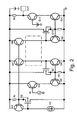
- FIG. 1 shows a basic configuration of a constant current circuit according to an embodiment of the present invention.
- a PNP transistor Q 1 has an emitter connected to a positive power supply and a collector connected via a constant current source CC to ground.
- a base of the transistor Q 1 which is a control end of the transistor Q 1 is connected to the positive power supply through a resistance R 1 and also connected to a collector of a PNP transistor Q 2 .
- a base of the transistor Q 2 is connected to the collector of the transistor Q 1 , while a collector of the transistor Q 2 is connected to ground.
- a base line of the transistor Q 1 is connected to PNP transistors Q 7 and Q 8 whose emitters are connected to the positive power supply, and a base current is supplied from the transistor Q 2 to the base line.
- the transistors Q 7 and Q 8 constitute a current mirror circuit in conjunction with the transistor Q 1 .
- an NPN transistor Q 4 has a base to which a signal IN is input, a collector connected to the positive power supply, and an emitter connected to a collector of an NPN transistor Q 3 .
- An emitter of the transistor Q 3 is connected to ground, while a base of the transistor Q 3 is connected to ground through a resistance R 2 and also connected to both a base of an NPN transistor Q 6 and an emitter of an NPN transistor Q 5 .
- the transistor Q 6 has an emitter connected to ground and a collector connected to a base of the NPN transistor Q 5 .
- the transistor Q 5 has a collector connected to the positive power supply and an emitter connected to a common base for the transistors Q 3 and Q 6 . Therefore, the transistor Q 6 and the transistor Q 3 constitute a current mirror.
- both the collector of the transistor Q 6 and the base of the transistor Q 5 are connected to a collector of the transistor Q 7 .
- a constant current corresponding to a current that flows through the transistor Q 1 is fed from the transistor Q 7 , and the constant current flows through both the transistor Q 6 and the transistor Q 3 . Therefore, the constant current flows through the transistor Q 4 as a bias current, which causes the transistor Q 4 to output a current corresponding to the input signal IN from an output terminal OUT 0 disposed on a collector side of the transistor Q 4 .
- a collector of the transistor Q 8 is connected to a collector of an NPN transistor Q 9 whose emitter is connected to ground.
- a collector of the transistor Q 9 is connected to a base of an NPN transistor Q 10 , and a collector of the transistor Q 10 is connected to the positive power supply while an emitter of the transistor Q 10 is connected to a base of the transistor Q 9 .
- the base of the transistor Q 9 is connected to ground through a resistance R 3 and also connected to a base of an NPN transistor Q 11 .
- the transistor Q 11 has an emitter connected to ground, and constitutes a current mirror in conjunction with the transistor Q 9 .
- a collector of the transistor Q 11 is connected to an emitter of an NPN transistor Q 12 .
- a collector of the transistor Q 12 is connected to the positive power supply through a resistance R 4 , and a signal IN 2 is input to a base of the transistor Q 12 .
- an output terminal OUT is connected to a collector of the transistor Q 12 .
- the constant current that flows through the transistor Q 1 is sent to the transistor Q 11 and then supplied as the bias current to the transistor Q 12 . Accordingly, a voltage output in accordance with ah input to the transistor Q 12 is obtained at the output terminal OUT.
- the transistor Q 1 forms the current mirror together with the transistors Q 7 and Q 8 , and the transistors Q 7 and Q 8 function as a constant current source.
- the transistors Q 7 and Q 8 are circuits for handling different signals.
- the output terminal OUT 0 is removed from the circuit, and the input to the base of the transistor Q 12 is supplied at a constant voltage. Accordingly, the output terminal OUT 0 is removed from the circuits of from FIG. 2 onward, and the input to the base of the transistor Q 12 is represented as a direct-current power supply.
- the transistors Q 2 , Q 5 , and Q 10 disposed between the base and the collector of the transistor Q 1 which is located on an input side of the current mirror are composed of MOS transistors.
- the transistors Q 2 , Q 5 , and Q 10 function to provide the base current to the transistors that form the current mirror.
- the MOS transistors which do not need the base current are used as the transistors Q 2 , Q 5 , and Q 10 , the current mirror can be configured with a high degree of accuracy.
- the transistors Q 1 , Q 2 , Q 7 , and Q 8 that constitute the current mirror circuit for supplying the constant current from the constant current source CC shown in FIG. 1 are composed of NPN transistors. Accordingly, the transistors Q 3 , Q 5 , Q 6 , Q 9 , Q 10 , and Q 11 that constitute another current mirror circuit are composed of PNP transistors. Also in this circuit, the current that flows through the constant current source CC is supplied via the transistors Q 7 and Q 8 to the transistors Q 4 and Q 12 as the bias current, and the inputs to the bases of the transistors Q 4 and Q 12 are respectively obtained at output terminals of the transistors Q 4 and Q 12 .
- FIG. 4 shows an example of using the MOS transistors as the transistors Q 2 , Q 5 , and Q 10 in the circuit of FIG. 3 .
- the input signal acts on the emitter of the transistor Q 12 , thereby causing the transistor Q 12 to operate.
- the input signal leaks from the collector of the transistor Q 12 to the output terminal.
- the circuit of FIG. 1 can be simplified as illustrated in FIG. 5 .
- the circuit of FIG. 5 is developed by removing the transistors Q 3 , Q 5 , Q 6 , Q 9 , Q 10 , and Q 11 , a circuit as shown in FIG. 6 is obtained.
- the transistors Q 1 and Q 2 are represented simply by diodes and the transistors Q 7 and Q 8 are represented only by direct current power supplies in the circuit of FIG. 6 , the circuit can be also depicted as shown in FIG. 7 .
- FIG. 9 the most simplified diagram of the above-described circuit is shown in FIG. 9 .
- the direct current power supplies are omitted, and the CB capacitances of the transistors Q 7 and Q 8 are described as capacitances in their original forms.
- a low pass filter is mounted between an output collector and a part that receives a current from the output collector, to thereby eliminate the DC change which results in the signal leakage.
- a low pass filter LPF is inserted, as illustrated in FIG. 10 , between an input signal source and the collector of the transistor Q 7 and between the collector of the transistor Q 8 and the output terminal OUT for outputting the signal, to remove, in the low pass filter LPF, the high-frequency component from the signal with a view toward preventing the signal leakage being transferred over the base line of the current mirror circuit.
- FIG. 8 A slightly more detailed illustration of the circuit of FIG. 10 is shown in FIG. 8 .
- the low pass filter LPF is preferably configured in a form as depicted in FIG. 11A , 11 B, 11 C, or 11 D.
- FIG. 11A a connection point between two resistances connected in series is connected to one end of a capacitance whose the other end is connected to ground.
- FIG. 11B a lower side (a ground side) of one resistance is connected to one end of the capacitance whose other end is connected to ground.
- FIG. 11C an upper side (a positive power supply side) of one resistance is connected to one end of the capacitance whose other end is connected to ground.
- the low pass filter LPF may be configured by only the resistance as shown in FIG. 12 .
- various types of transistors are formed by implanting impurities into a silicon substrate to thereby form an N well, a P well, an N region, a P region, and others. Accordingly, the parasitic capacitance is generated between a collector (C) region and the substrate (SUB).
- this parasitic capacitance can be used as a capacitance for the low pass filter LPF.
- Such usage of the capacitance allows the high-frequency component to escape to a substrate side.
- the low pass filter LPF can be formed on a wiring line by disposing the resistance on the wiring line for connecting the collectors of the transistor Q 7 and of the transistor Q 6 , or by disposing the resistance on a wiring line for connecting the collectors of the transistor Q 8 and of the transistor Q 10 .
- FIGS. 13A , 14 A, 15 A, and 16 A show circuits according to other embodiments. It should be noted that a signal output corresponding to an input to the transistor Q 4 is not illustrated in FIGS. 13A , 14 A, 15 A, and 16 A.
- the low pass filter LPF using the series resistances and the capacitance in combination as shown in FIG. 11A is mounted on both the wiring line for connecting the collectors of the transistor Q 7 and of the transistor Q 6 , and the wiring line for connecting the collectors of the transistor Q 8 and of the transistor Q 10 .
- FIGS. 13B , 14 B, 15 B, and 16 B are diagrams each showing an effect obtained by the provision of the low pass filter LPF as described above.
- a curve designated as “NEW CIRCUIT” represents the circuit according to the embodiment. It can be seen from the drawings that signal leakage is suppressed in a wide range of from several megahertzs (MHz) to 1 gigahertz (GHz).
- FIG. 13A shows the circuit configured by adding the low pass filters LPFs into the circuit shown in FIG. 1
- FIG. 14A shows the circuit configured by adding the low pass filters LPFs into the circuit shown in FIG. 2
- FIG. 15A shows the circuit configured by adding the low pass filters LPFs into the circuit shown in FIG. 3
- FIG. 16A shows the circuit configured by adding the low pass filters LPFs into the circuit shown in FIG. 4 .
- FIGS. 17 , 18 , 19 , and 20 show application examples of the present embodiment.
- the base line of one current mirror input transistor Q 1 is connected to multiple current mirror output transistors Q 20 s from which the constant currents are respectively output, and the output constant currents are supplied to respective output terminals.
- the low pass filter LPF is disposed on each current path between the current mirror output transistors Q 20 s and the output terminals, to remove the high-frequency component through the low pass filter LPF on the current path.
- the current mirror circuit including the low pass filters is integrated into one cell, and the outputs from the current mirror output transistors Q 20 s is connected to output terminals of the cell to respectively supply the constant current via the output terminals of the cell to operation circuits installed outside the cell.
- the current mirror circuit having a plurality of the constant current outputs is integrated into one cell, and the low pass filter is mounted on a part from which the constant currents are output, to thereby remove the high-frequency component. In this manner, a high-frequency signal being transferred from one output terminal via the base line of the current mirror circuit to another output terminal can be prevented.
- the transistors may be configured using the MOS transistors, which has not explained in the description above.
- the PNP type corresponds to a P channel
- the NPN type corresponds to an N channel
- the collector corresponds to a drain
- the emitter corresponds to a source
- the base corresponds to the gate (the control end).
Landscapes
- Engineering & Computer Science (AREA)
- Physics & Mathematics (AREA)
- Microelectronics & Electronic Packaging (AREA)
- Nonlinear Science (AREA)
- Electromagnetism (AREA)
- General Physics & Mathematics (AREA)
- Radar, Positioning & Navigation (AREA)
- Automation & Control Theory (AREA)
- Amplifiers (AREA)
- Control Of Electrical Variables (AREA)
- Networks Using Active Elements (AREA)
Abstract
Description
Claims (5)
Applications Claiming Priority (2)
| Application Number | Priority Date | Filing Date | Title |
|---|---|---|---|
| JP2006351118A JP5237549B2 (en) | 2006-12-27 | 2006-12-27 | Constant current circuit |
| JP2006-351118 | 2006-12-27 |
Publications (2)
| Publication Number | Publication Date |
|---|---|
| US20080174294A1 US20080174294A1 (en) | 2008-07-24 |
| US7902808B2 true US7902808B2 (en) | 2011-03-08 |
Family
ID=39640604
Family Applications (1)
| Application Number | Title | Priority Date | Filing Date |
|---|---|---|---|
| US11/963,412 Expired - Fee Related US7902808B2 (en) | 2006-12-27 | 2007-12-21 | Constant current circuit for supplying a constant current to operating circuits |
Country Status (2)
| Country | Link |
|---|---|
| US (1) | US7902808B2 (en) |
| JP (1) | JP5237549B2 (en) |
Citations (18)
| Publication number | Priority date | Publication date | Assignee | Title |
|---|---|---|---|---|
| JPH07121256A (en) | 1993-10-26 | 1995-05-12 | Sanyo Electric Co Ltd | Current mirror circuit |
| US5627490A (en) * | 1995-02-23 | 1997-05-06 | Matsushita Electric Industrial Co., Ltd. | Amplifier circuit |
| JPH1097332A (en) | 1996-09-20 | 1998-04-14 | Sanyo Electric Co Ltd | Current mirror circuit |
| US6084391A (en) * | 1998-06-05 | 2000-07-04 | Nec Corporation | Bandgap reference voltage generating circuit |
| US6150885A (en) * | 1999-06-24 | 2000-11-21 | Lucent Technologies Inc. | Transconductance amplifier with wideband noise filtering |
| US6184742B1 (en) * | 1996-09-26 | 2001-02-06 | U.S. Philips Corporation | Current distribution circuit having an additional parallel DC-current sinking branch |
| US20020079968A1 (en) * | 2000-12-22 | 2002-06-27 | Godfrey Paul J. | Common mode output current control circuit and method |
| US6429720B1 (en) * | 2000-05-12 | 2002-08-06 | Analog Devices, Inc. | RMS-DC converter using a variable gain amplifier to drive a squaring cell |
| US6465997B2 (en) * | 2000-09-15 | 2002-10-15 | Stmicroelectronics S.A. | Regulated voltage generator for integrated circuit |
| US6472928B1 (en) * | 2001-05-04 | 2002-10-29 | Semiconductor Components Industries Llc | Reduced noise band gap reference with current feedback and method of using |
| US6496057B2 (en) * | 2000-08-10 | 2002-12-17 | Sanyo Electric Co., Ltd. | Constant current generation circuit, constant voltage generation circuit, constant voltage/constant current generation circuit, and amplification circuit |
| US6545540B1 (en) * | 2000-10-11 | 2003-04-08 | Intersil Americas Inc. | Current mirror-embedded low-pass filter for subscriber line interface circuit applications |
| US6668334B1 (en) * | 2000-06-27 | 2003-12-23 | Lucent Technologies Inc. | Apparatus for detecting clock failure within a fixed number of cycles of the clock |
| US6784652B1 (en) * | 2003-02-25 | 2004-08-31 | National Semiconductor Corporation | Startup circuit for bandgap voltage reference generator |
| US20050248393A1 (en) * | 2004-05-05 | 2005-11-10 | Elantec Semiconductor, Inc. | Noise cancellation circuits and methods |
| JP2006033523A (en) | 2004-07-16 | 2006-02-02 | Sanyo Electric Co Ltd | Current mirror circuit |
| US6998902B2 (en) * | 2001-10-26 | 2006-02-14 | Oki Electric Industry Co., Ltd. | Bandgap reference voltage circuit |
| US7132899B1 (en) * | 2004-10-22 | 2006-11-07 | Xilinx, Inc. | Method and apparatus for providing an improved high speed buffer |
Family Cites Families (8)
| Publication number | Priority date | Publication date | Assignee | Title |
|---|---|---|---|---|
| JPH01115203A (en) * | 1987-10-29 | 1989-05-08 | Mitsubishi Electric Corp | Current mirror circuit |
| JP2708442B2 (en) * | 1987-12-11 | 1998-02-04 | 株式会社日立製作所 | Semiconductor integrated circuit |
| JPH10163429A (en) * | 1996-11-29 | 1998-06-19 | Mitsubishi Electric Corp | Semiconductor device |
| JP2000252779A (en) * | 1999-02-26 | 2000-09-14 | Kyocera Corp | RC filter |
| CA2454723C (en) * | 2001-07-23 | 2010-07-20 | Northern Power Systems, Inc. | Control system for a power converter and method of controlling operation of a power converter prior application information |
| JP2005197859A (en) * | 2004-01-05 | 2005-07-21 | Renesas Technology Corp | High frequency power amplifier circuit |
| JP2005348312A (en) * | 2004-06-07 | 2005-12-15 | Renesas Technology Corp | Electronic components for high frequency power amplification |
| JP2006060455A (en) * | 2004-08-19 | 2006-03-02 | Matsushita Electric Ind Co Ltd | Constant current mirror circuit |
-
2006
- 2006-12-27 JP JP2006351118A patent/JP5237549B2/en not_active Expired - Fee Related
-
2007
- 2007-12-21 US US11/963,412 patent/US7902808B2/en not_active Expired - Fee Related
Patent Citations (21)
| Publication number | Priority date | Publication date | Assignee | Title |
|---|---|---|---|---|
| JPH07121256A (en) | 1993-10-26 | 1995-05-12 | Sanyo Electric Co Ltd | Current mirror circuit |
| US5627490A (en) * | 1995-02-23 | 1997-05-06 | Matsushita Electric Industrial Co., Ltd. | Amplifier circuit |
| JPH1097332A (en) | 1996-09-20 | 1998-04-14 | Sanyo Electric Co Ltd | Current mirror circuit |
| US6184742B1 (en) * | 1996-09-26 | 2001-02-06 | U.S. Philips Corporation | Current distribution circuit having an additional parallel DC-current sinking branch |
| US6084391A (en) * | 1998-06-05 | 2000-07-04 | Nec Corporation | Bandgap reference voltage generating circuit |
| US6150885A (en) * | 1999-06-24 | 2000-11-21 | Lucent Technologies Inc. | Transconductance amplifier with wideband noise filtering |
| US6696888B2 (en) * | 2000-05-12 | 2004-02-24 | Analog Devices, Inc. | Amplifier with feedback compensation |
| US6429720B1 (en) * | 2000-05-12 | 2002-08-06 | Analog Devices, Inc. | RMS-DC converter using a variable gain amplifier to drive a squaring cell |
| US6525601B2 (en) * | 2000-05-12 | 2003-02-25 | Analog Devices, Inc. | Input system for variable gain amplifier having transconductance stages with feedforward paths diverted to AC ground |
| US6668334B1 (en) * | 2000-06-27 | 2003-12-23 | Lucent Technologies Inc. | Apparatus for detecting clock failure within a fixed number of cycles of the clock |
| US6496057B2 (en) * | 2000-08-10 | 2002-12-17 | Sanyo Electric Co., Ltd. | Constant current generation circuit, constant voltage generation circuit, constant voltage/constant current generation circuit, and amplification circuit |
| US6465997B2 (en) * | 2000-09-15 | 2002-10-15 | Stmicroelectronics S.A. | Regulated voltage generator for integrated circuit |
| US6545540B1 (en) * | 2000-10-11 | 2003-04-08 | Intersil Americas Inc. | Current mirror-embedded low-pass filter for subscriber line interface circuit applications |
| US20020079968A1 (en) * | 2000-12-22 | 2002-06-27 | Godfrey Paul J. | Common mode output current control circuit and method |
| US6472928B1 (en) * | 2001-05-04 | 2002-10-29 | Semiconductor Components Industries Llc | Reduced noise band gap reference with current feedback and method of using |
| US6998902B2 (en) * | 2001-10-26 | 2006-02-14 | Oki Electric Industry Co., Ltd. | Bandgap reference voltage circuit |
| US6784652B1 (en) * | 2003-02-25 | 2004-08-31 | National Semiconductor Corporation | Startup circuit for bandgap voltage reference generator |
| US20050248393A1 (en) * | 2004-05-05 | 2005-11-10 | Elantec Semiconductor, Inc. | Noise cancellation circuits and methods |
| US20060061414A1 (en) * | 2004-05-05 | 2006-03-23 | Elantec Semiconductor, Inc. | Noise cancellation circuits and methods |
| JP2006033523A (en) | 2004-07-16 | 2006-02-02 | Sanyo Electric Co Ltd | Current mirror circuit |
| US7132899B1 (en) * | 2004-10-22 | 2006-11-07 | Xilinx, Inc. | Method and apparatus for providing an improved high speed buffer |
Non-Patent Citations (3)
| Title |
|---|
| esp@cenet patent abstract for Japanese Publication No. 10097332, Publication date Apr. 14, 1998 (1 page). |
| esp@cenet patent abstract for Japanese Publication No. 2006033523, Publication date Feb. 2, 2006 (1 page). |
| esp@cenet patent abstract for Japanese Publication No. 7121256, Publication date May 12, 1995 (1 page). |
Also Published As
| Publication number | Publication date |
|---|---|
| JP2008166904A (en) | 2008-07-17 |
| JP5237549B2 (en) | 2013-07-17 |
| US20080174294A1 (en) | 2008-07-24 |
Similar Documents
| Publication | Publication Date | Title |
|---|---|---|
| US8279003B2 (en) | Differential RF amplifier | |
| US6850120B2 (en) | Semiconductor device including semiconductor element of high breakdown voltage | |
| US6819182B2 (en) | High isolation/high speed buffer amplifier | |
| JP3886090B2 (en) | Differential amplifier circuit | |
| US20040263211A1 (en) | On-chip high-pass filter with large time constant | |
| US7948329B2 (en) | Oscillator gain circuit and method | |
| US9401679B1 (en) | Apparatus and method for improving power supply rejection ratio | |
| US20190158024A1 (en) | Crystal oscillator interconnect architecture with noise immunity | |
| US20220385244A1 (en) | Multiple feedback filter | |
| US7227392B2 (en) | Frequency multiplier | |
| US7902808B2 (en) | Constant current circuit for supplying a constant current to operating circuits | |
| US7209010B2 (en) | Oscillator with tunable diffusion capacitance as resonant circuit capacitance | |
| US20030107429A1 (en) | Current source circuit | |
| US7002396B2 (en) | Frequency converter | |
| US11869399B2 (en) | Driving circuit and semiconductor integrated circuit for use in an optical communication device | |
| US7286018B2 (en) | Transistor circuit | |
| EP1280033B1 (en) | EMC immune low drop regulator | |
| US4799028A (en) | Zero phase shift active microwave oscillators with resistive feedback in field effect transistor amplifiers | |
| CN117674745A (en) | Amplifying circuit and communication device | |
| US7193483B2 (en) | Blocking a leakage current | |
| JP2010273284A (en) | High frequency amplifier | |
| US6255868B1 (en) | Buffer circuit and hold circuit | |
| JP5448044B2 (en) | High frequency amplifier circuit and communication equipment | |
| US7567787B2 (en) | Apparatus and method of feeding internal calibration signal through electro-static discharge protection circuitry | |
| US20080068088A1 (en) | Amplifier circuit |
Legal Events
| Date | Code | Title | Description |
|---|---|---|---|
| AS | Assignment |
Owner name: SANYO SEMICONDUCTOR CO., LTD., JAPAN Free format text: ASSIGNMENT OF ASSIGNORS INTEREST;ASSIGNOR:HASHIMOTO, FUMINORI;REEL/FRAME:020318/0163 Effective date: 20071217 Owner name: SANYO ELECTRIC CO., LTD., JAPAN Free format text: ASSIGNMENT OF ASSIGNORS INTEREST;ASSIGNOR:HASHIMOTO, FUMINORI;REEL/FRAME:020318/0163 Effective date: 20071217 |
|
| STCF | Information on status: patent grant |
Free format text: PATENTED CASE |
|
| AS | Assignment |
Owner name: SEMICONDUCTOR COMPONENTS INDUSTRIES, LLC, ARIZONA Free format text: ASSIGNMENT OF ASSIGNORS INTEREST;ASSIGNOR:SANYO ELECTRIC CO., LTD.;REEL/FRAME:026594/0385 Effective date: 20110101 |
|
| AS | Assignment |
Owner name: SEMICONDUCTOR COMPONENTS INDUSTRIES, LLC, ARIZONA Free format text: CORRECTIVE ASSIGNMENT TO CORRECT THE INCORRECT #12/577882 PREVIOUSLY RECORDED ON REEL 026594 FRAME 0385. ASSIGNOR(S) HEREBY CONFIRMS THE ASSIGNMENT;ASSIGNOR:SANYO ELECTRIC CO., LTD;REEL/FRAME:032836/0342 Effective date: 20110101 |
|
| FPAY | Fee payment |
Year of fee payment: 4 |
|
| AS | Assignment |
Owner name: SEMICONDUCTOR COMPONENTS INDUSTRIES, LLC, ARIZONA Free format text: ASSIGNMENT OF ASSIGNORS INTEREST;ASSIGNOR:SANYO SEMICONDUCTOR CO., LTD.;REEL/FRAME:033813/0420 Effective date: 20140924 |
|
| AS | Assignment |
Owner name: SYSTEM SOLUTIONS CO., LTD., JAPAN Free format text: CHANGE OF NAME;ASSIGNOR:SANYO SEMICONDUCTOR CO., LTD;REEL/FRAME:034537/0044 Effective date: 20140228 |
|
| AS | Assignment |
Owner name: SEMICONDUCTOR COMPONENTS INDUSTRIES, LLC, ARIZONA Free format text: CORRECTIVE ASSIGNMENT TO CORRECT THE ASSIGNOR NAME PREVIOUSLY RECORDED AT REEL: 033813 FRAME: 0420. ASSIGNOR(S) HEREBY CONFIRMS THE ASSIGNMENT;ASSIGNOR:SYSTEM SOLUTIONS CO., LTD.;REEL/FRAME:034816/0510 Effective date: 20141217 |
|
| AS | Assignment |
Owner name: DEUTSCHE BANK AG NEW YORK BRANCH, NEW YORK Free format text: SECURITY INTEREST;ASSIGNOR:SEMICONDUCTOR COMPONENTS INDUSTRIES, LLC;REEL/FRAME:038620/0087 Effective date: 20160415 |
|
| AS | Assignment |
Owner name: DEUTSCHE BANK AG NEW YORK BRANCH, AS COLLATERAL AGENT, NEW YORK Free format text: CORRECTIVE ASSIGNMENT TO CORRECT THE INCORRECT PATENT NUMBER 5859768 AND TO RECITE COLLATERAL AGENT ROLE OF RECEIVING PARTY IN THE SECURITY INTEREST PREVIOUSLY RECORDED ON REEL 038620 FRAME 0087. ASSIGNOR(S) HEREBY CONFIRMS THE SECURITY INTEREST;ASSIGNOR:SEMICONDUCTOR COMPONENTS INDUSTRIES, LLC;REEL/FRAME:039853/0001 Effective date: 20160415 Owner name: DEUTSCHE BANK AG NEW YORK BRANCH, AS COLLATERAL AG Free format text: CORRECTIVE ASSIGNMENT TO CORRECT THE INCORRECT PATENT NUMBER 5859768 AND TO RECITE COLLATERAL AGENT ROLE OF RECEIVING PARTY IN THE SECURITY INTEREST PREVIOUSLY RECORDED ON REEL 038620 FRAME 0087. ASSIGNOR(S) HEREBY CONFIRMS THE SECURITY INTEREST;ASSIGNOR:SEMICONDUCTOR COMPONENTS INDUSTRIES, LLC;REEL/FRAME:039853/0001 Effective date: 20160415 |
|
| MAFP | Maintenance fee payment |
Free format text: PAYMENT OF MAINTENANCE FEE, 8TH YEAR, LARGE ENTITY (ORIGINAL EVENT CODE: M1552); ENTITY STATUS OF PATENT OWNER: LARGE ENTITY Year of fee payment: 8 |
|
| FEPP | Fee payment procedure |
Free format text: MAINTENANCE FEE REMINDER MAILED (ORIGINAL EVENT CODE: REM.); ENTITY STATUS OF PATENT OWNER: LARGE ENTITY |
|
| LAPS | Lapse for failure to pay maintenance fees |
Free format text: PATENT EXPIRED FOR FAILURE TO PAY MAINTENANCE FEES (ORIGINAL EVENT CODE: EXP.); ENTITY STATUS OF PATENT OWNER: LARGE ENTITY |
|
| STCH | Information on status: patent discontinuation |
Free format text: PATENT EXPIRED DUE TO NONPAYMENT OF MAINTENANCE FEES UNDER 37 CFR 1.362 |
|
| FP | Lapsed due to failure to pay maintenance fee |
Effective date: 20230308 |
|
| AS | Assignment |
Owner name: FAIRCHILD SEMICONDUCTOR CORPORATION, ARIZONA Free format text: RELEASE OF SECURITY INTEREST IN PATENTS RECORDED AT REEL 038620, FRAME 0087;ASSIGNOR:DEUTSCHE BANK AG NEW YORK BRANCH, AS COLLATERAL AGENT;REEL/FRAME:064070/0001 Effective date: 20230622 Owner name: SEMICONDUCTOR COMPONENTS INDUSTRIES, LLC, ARIZONA Free format text: RELEASE OF SECURITY INTEREST IN PATENTS RECORDED AT REEL 038620, FRAME 0087;ASSIGNOR:DEUTSCHE BANK AG NEW YORK BRANCH, AS COLLATERAL AGENT;REEL/FRAME:064070/0001 Effective date: 20230622 |