US7193483B2 - Blocking a leakage current - Google Patents
Blocking a leakage current Download PDFInfo
- Publication number
- US7193483B2 US7193483B2 US11/089,310 US8931005A US7193483B2 US 7193483 B2 US7193483 B2 US 7193483B2 US 8931005 A US8931005 A US 8931005A US 7193483 B2 US7193483 B2 US 7193483B2
- Authority
- US
- United States
- Prior art keywords
- circuit
- oscillator
- leakage current
- amplifier
- coupled
- Prior art date
- Legal status (The legal status is an assumption and is not a legal conclusion. Google has not performed a legal analysis and makes no representation as to the accuracy of the status listed.)
- Active, expires
Links
- 230000000903 blocking effect Effects 0.000 title description 9
- 239000004065 semiconductor Substances 0.000 claims description 36
- 239000013078 crystal Substances 0.000 claims description 23
- 239000003990 capacitor Substances 0.000 claims description 16
- 238000000034 method Methods 0.000 claims description 14
- 230000008878 coupling Effects 0.000 claims description 7
- 238000010168 coupling process Methods 0.000 claims description 7
- 238000005859 coupling reaction Methods 0.000 claims description 7
- 230000001105 regulatory effect Effects 0.000 claims 1
- 238000010586 diagram Methods 0.000 description 8
- 239000002131 composite material Substances 0.000 description 7
- 230000008569 process Effects 0.000 description 5
- 230000008859 change Effects 0.000 description 4
- 238000013461 design Methods 0.000 description 3
- 230000008901 benefit Effects 0.000 description 2
- 230000007423 decrease Effects 0.000 description 2
- 238000005421 electrostatic potential Methods 0.000 description 2
- 238000012986 modification Methods 0.000 description 2
- 230000004048 modification Effects 0.000 description 2
- 238000012358 sourcing Methods 0.000 description 2
- 230000002411 adverse Effects 0.000 description 1
- 238000004364 calculation method Methods 0.000 description 1
- 230000001413 cellular effect Effects 0.000 description 1
- 238000004891 communication Methods 0.000 description 1
- 239000000463 material Substances 0.000 description 1
- 239000002184 metal Substances 0.000 description 1
- 229910044991 metal oxide Inorganic materials 0.000 description 1
- 150000004706 metal oxides Chemical class 0.000 description 1
- 230000010355 oscillation Effects 0.000 description 1
- 230000002269 spontaneous effect Effects 0.000 description 1
- 230000000087 stabilizing effect Effects 0.000 description 1
- 238000012546 transfer Methods 0.000 description 1
Images


Classifications
-
- H—ELECTRICITY
- H03—ELECTRONIC CIRCUITRY
- H03B—GENERATION OF OSCILLATIONS, DIRECTLY OR BY FREQUENCY-CHANGING, BY CIRCUITS EMPLOYING ACTIVE ELEMENTS WHICH OPERATE IN A NON-SWITCHING MANNER; GENERATION OF NOISE BY SUCH CIRCUITS
- H03B5/00—Generation of oscillations using amplifier with regenerative feedback from output to input
- H03B5/30—Generation of oscillations using amplifier with regenerative feedback from output to input with frequency-determining element being electromechanical resonator
- H03B5/32—Generation of oscillations using amplifier with regenerative feedback from output to input with frequency-determining element being electromechanical resonator being a piezoelectric resonator
- H03B5/36—Generation of oscillations using amplifier with regenerative feedback from output to input with frequency-determining element being electromechanical resonator being a piezoelectric resonator active element in amplifier being semiconductor device
- H03B5/364—Generation of oscillations using amplifier with regenerative feedback from output to input with frequency-determining element being electromechanical resonator being a piezoelectric resonator active element in amplifier being semiconductor device the amplifier comprising field effect transistors
-
- H—ELECTRICITY
- H03—ELECTRONIC CIRCUITRY
- H03B—GENERATION OF OSCILLATIONS, DIRECTLY OR BY FREQUENCY-CHANGING, BY CIRCUITS EMPLOYING ACTIVE ELEMENTS WHICH OPERATE IN A NON-SWITCHING MANNER; GENERATION OF NOISE BY SUCH CIRCUITS
- H03B5/00—Generation of oscillations using amplifier with regenerative feedback from output to input
- H03B5/30—Generation of oscillations using amplifier with regenerative feedback from output to input with frequency-determining element being electromechanical resonator
- H03B5/32—Generation of oscillations using amplifier with regenerative feedback from output to input with frequency-determining element being electromechanical resonator being a piezoelectric resonator
- H03B5/36—Generation of oscillations using amplifier with regenerative feedback from output to input with frequency-determining element being electromechanical resonator being a piezoelectric resonator active element in amplifier being semiconductor device
- H03B5/362—Generation of oscillations using amplifier with regenerative feedback from output to input with frequency-determining element being electromechanical resonator being a piezoelectric resonator active element in amplifier being semiconductor device the amplifier being a single transistor
Definitions
- the invention generally relates to blocking a leakage current.
- a typical semiconductor package includes one or more semiconductor dies that contain integrated circuitry and external terminals (leads or bumps, for example) to electrically connect the package to other electrical components.
- the die(s) typically contain bonding pads, which are exposed sites on the die(s) at which electrically conductive bonds are formed between the integrated circuitry and the external terminals of the semiconductor package.
- Each external terminal of the semiconductor package may potentially communicate an electrostatic discharge (ESD) to the integrated circuitry of the package.
- ESD electrostatic discharge
- An ESD is a rapid and spontaneous transfer of electrostatic charge between two bodies, which is initiated by an electrostatic potential difference between the bodies.
- an ESD may occur, for example, when a particular external terminal of the semiconductor package contacts a body (a machine, a human body, a shipping material, etc.) that has a different electrostatic potential.
- the ESD typically produces a voltage fluctuation, or spike, on the external terminal; and this voltage spike may be capable of damaging integrated circuitry of the semiconductor package.
- a conventional integrated circuit may have an ESD protection circuit for each bonding pad to reduce, or dampen, an ESD-induced voltage spike that may otherwise propagate to the pad and onto other circuitry that is electrically coupled to the pad.
- an apparatus in an embodiment of the invention, includes an oscillator circuit that includes terminals to couple a second circuit having an impedance to the oscillator circuit.
- the apparatus includes a third circuit that is coupled to at least one of the terminals to isolate a leakage current from at least part of the oscillator circuit.
- a technique in another embodiment, includes coupling an electrostatic discharge protection circuit to an oscillator and isolating a leakage current that is generated by the electrostatic discharge protection circuit from at least part of the oscillator.
- a system in another embodiment, includes an oscillator circuit to provide a reference signal.
- the oscillator circuit includes terminals to couple a second circuit that has an impedance to the oscillator circuit.
- the system also includes an electrostatic discharge circuit, a fourth circuit and a radio frequency circuit.
- the electrostatic discharge protection circuit is coupled to one of the terminals and is capable of generating a leakage current.
- the fourth circuit isolates the leakage current from at least part of the oscillator circuit, and the radio frequency circuit receives the reference signal.
- an apparatus in yet another embodiment, includes a semiconductor die and a circuit.
- the die includes oscillator circuitry, and the circuit isolates leakage current from at least part of the oscillator circuitry.
- FIG. 1 is a schematic diagram of an integrated circuit oscillator according to an embodiment of the invention.
- FIG. 2 is a schematic diagram of an oscillator.
- FIG. 3 is a schematic diagram illustrating the impedances of a crystal.
- FIG. 4 is a schematic diagram of a portion of the oscillator of FIG. 4 used in an impedance calculation.
- FIG. 5 is a schematic diagram depicting an equivalent impedance of the portion of the oscillator shown in FIG. 4 .
- FIG. 6 is a schematic diagram illustrating the impedances of the oscillator of FIG. 4 .
- FIG. 7 is a schematic diagram of an integrated circuit oscillator according to an embodiment of the invention.
- FIG. 8 is a schematic diagram of a wireless system according to an embodiment of the invention.
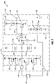
- an embodiment 20 of an oscillator in accordance with the invention includes an oscillator circuit 24 that is fabricated on a semiconductor die 22 and a crystal 32 that is external to the die 22 .
- the oscillator circuit 24 includes an amplifier and impedances, at least some of which are coupled to the crystal 32 to form a resonant tank for the oscillator 20 .
- the oscillator 20 generates an analog sinusoidal signal (called “V OUT ” in FIG. 1 ) at its output terminals 26 .
- the V OUT signal may be a reference signal for a transceiver.
- the semiconductor die 22 may be part of a semiconductor package that includes external crystal connection terminals 27 (e.g., leads or bumps).
- external crystal connection terminals 27 e.g., leads or bumps.
- bonding pads 30 of the semiconductor die 22 are bonded and electrically coupled to the external crystal connection terminals 27 ; and through one or more metal layers that formed in the semiconductor die 22 , the bonding pads 30 are electrically connected to internal crystal connection terminals 28 that extend to the oscillator circuit 24 .
- the bonding pads 30 are located between the external crystal connection terminals 27 of the semiconductor package and the internal crystal connection terminals 28 .
- the semiconductor die 22 may include electrostatic discharge (ESD) protection circuits 29 for purposes of protecting the oscillator 20 from ESD-induced voltage spikes. As depicted in FIG. 1 , each bonding pad 30 may be connected to an associated ESD protection circuit 29 . It is noted that the ESD protection circuits 29 may be external to the die 22 , in some embodiments of the invention.
- ESD electrostatic discharge
- the ESD protection circuit 29 may include one or more diodes that are capable of generating a composite DC leakage current (called “I LEAK ” in FIG. 1 ) into or out of the oscillator 20 , if not for features of the oscillator 20 described herein.
- the leakage current is attributable to conduction of current through the diodes of the ESD protection circuit 29 when the diodes are in their reverse biased states.
- Such a leakage current may significantly affect the DC biasing in one or more parts of the oscillator 20 and thus, may significantly alter operation of the oscillator 20 .
- the oscillator 20 includes a leakage current blocking circuit 36 to block, or isolate, leakage currents that are generated by the ESD protection circuits 29 from the parts of the oscillator 20 , which are sensitive to a leakage current.
- the oscillator circuit 24 may include a feedback resistor whose relatively high resistance (a resistance in the megaohm range, for example) causes at least part of the oscillator circuit 24 to be sensitive to small changes in the current that flows through the feedback resistor. More particularly, as further described below by way of a specific example, if not for the leakage current blocking circuit 36 , the large resistance of the feedback resistor is prone to magnifying any leakage current to the extent that biasing of the oscillator circuit 24 may be significantly altered.
- a feedback resistor whose relatively high resistance (a resistance in the megaohm range, for example) causes at least part of the oscillator circuit 24 to be sensitive to small changes in the current that flows through the feedback resistor. More particularly, as further described below by way of a specific example, if not for the leakage current blocking circuit 36 , the large resistance of the feedback resistor is prone to magnifying any leakage current to the extent that biasing of the oscillator circuit 24 may be significantly altered.
- a Colpitts-type oscillator such as a Colpitts oscillator 50 that is depicted in FIG. 2 , may be particularly sensitive to a leakage current.
- the oscillator 50 has a feedback resistor that has a relatively large feedback resistance; and due to this characteristic of the oscillator 50 , the presence of a leakage current in the feedback resistor may produce a DC voltage change that, in turn, significantly changes the DC biasing of the oscillator 50 from designed values.
- the oscillator 50 includes an amplifier 52 that is electrically coupled to a resonant tank 60 of the oscillator 50 .
- the resonant tank 60 includes a crystal 62 that is coupled between an input terminal 67 of the amplifier 52 and an output terminal 68 of the amplifier 52 .
- the resonant tank 60 also includes a capacitor 64 (having a capacitance called “C 1 ”) that is coupled between the input terminal 67 and ground.
- the resonant circuit 60 includes another capacitor 66 (having a capacitance called “C 2 ”) that is coupled between the output terminal 68 and ground.
- the amplifier 52 includes a current source 53 that is coupled between a positive supply voltage (called “V DD ”) and the output terminal 68 of the amplifier 52 .
- the current source 53 establishes a bias current for an n-channel metal oxide semiconductor field-effect-transistor (NMOSFET) 55 of the amplifier 52 .
- Drain 81 , gate 82 and source 83 terminals of the NMOSFET 55 are coupled to the output terminal 68 , input terminal 67 and ground, respectively.
- the amplifier 52 includes a feedback resistor 56 (having a resistance called “R b ”) that has one terminal, which is connected to the output terminal 68 ; and the other terminal of the feedback resistor 56 is connected to the input terminal 67 .
- the R b resistance of the feedback resistor 56 may be relatively large (a resistance in the megaohm range, for example) for purposes of stabilizing the operation of the oscillator 50 and producing an oscillation frequency that remains within a relatively tight tolerance.
- a large R b resistance means that the oscillator 50 is relatively sensitive to small changes in the current that flows through the resistor 56 .
- the oscillator 50 may be designed so that the current source 53 furnishes a constant current that in general does not vary with the drain voltage of the NMOSFET 55 , a leakage current may cause a larger-than-expected drain bias voltage of the NMOSFET 55 , which causes the current source 53 to undesirably linearly vary with the drain voltage or even turn off.
- the impedance of the crystal 62 may be viewed as being formed from the series connections of an inductor 72 (having an inductance called “L x ”), a resistor 76 (having a resistance called “R x ”) and a capacitor 74 (having a capacitance called “C x ”).
- an impedance (called “Z ON ”) of the oscillator 50 as viewed into the gate 81 and drain 82 terminals of the NMOSFET 55 may be mathematically described according to the following equation:
- Z ON - g m ⁇ 2 ⁇ C 1 ⁇ C 2 + 1 j ⁇ ⁇ ⁇ ⁇ C 1 + 1 j ⁇ ⁇ ⁇ ⁇ C 2 , Eq . ⁇ 1
- g m represents the transconductance of the NMOSFET 55 .
- the Z ON impedance may be represented by an equivalent circuit 90 ( FIG. 5 ) that includes a resistor 92 (having a resistance called “Req”) that is in series with a capacitor 94 (having a capacitance called “Ceq.”)
- the Req resistance and the Ceq capacitance are mathematically described below in Equations 2 and 3:
- the impedances of the oscillator 50 may be represented by an equivalent circuit 91 that is depicted in FIG. 6 .
- the circuit 91 is formed from the parallel connection of the Z ON impedance, the R b resistance and the impedance of the crystal 62 .
- the R b resistance is typically on the order of several megaohms (tens of megaohms, as a more specific example), a resistance value that may lead to problems if leakage current is routed to the resistor 56 .
- a 32 kilohertz (kHz) crystal that is typically available may have an Rx resistance (see FIG. 3 ) of 40 kilohms (k ⁇ ) to 2 k ⁇ and may use a load capacitance of 6 to 12.5 picoFarads (pF).
- Rx resistance see FIG. 3
- k ⁇ 40 kilohms
- pF load capacitance
- the Req resistance may be ⁇ 40 k ⁇
- the Ceq capacitance may be 8 pF.
- the series combination of the Req resistance and the Ceq capacitance may be transformed into a resistance that is parallel to a capacitance.
- the Rb resistance has to be much greater than 9.26 M ⁇ for purposes of making the overall negative resistance between the input 67 and output 68 terminals close to ⁇ 40 k ⁇ .
- the oscillator 50 has to adjust its operation point to accommodate the lower R b resistance. Therefore, a challenge with this low resistance is that the low resistance causes the equivalent load capacitance of the oscillator 50 to change, and this change may cause frequency error.
- a leakage current may produce a significant voltage drop across the resistor 56 .
- the R b resistance is 20 M ⁇
- 30 nanoamperes (nA) of leakage current produces a 600 millivolts (mV) voltage drop across the resistor 56
- nA nanoamperes
- mV millivolts
- This voltage drop forces the gate terminal voltage of the NMOSFET 55 to decrease and forces the drain terminal voltage of the NMOSFET 55 to increase.
- Possible solutions to de-sensitizing the oscillator's bias point to a leakage current include designing the oscillator 50 with a smaller R b resistance or limiting the operating temperature of the semiconductor package that contains the oscillator 50 . As pointed out above, a smaller R b resistance decreases the frequency stability of the oscillator. Furthermore, limiting the operation temperature of the semiconductor package may not be an optimal solution. Although it may be possible to design the ESD protection circuits to produce less leakage current, there is typically a tradeoff between the ESD protection performance of the ESD protection circuit and leakage current.
- an oscillator 100 may be used in place of the oscillator 50 .
- the oscillator 100 has a similar design to the oscillator 50 except for the following differences.
- the oscillator 100 includes a high pass filter that may be formed from a capacitor 108 , for example.
- the capacitor 108 serves as a leakage current blocking device for purposes of preventing a leakage current (i.e., a DC current) from either ESD protection circuit 120 or 126 from flowing through the resistor 56 , a bias sensitive part of the oscillator 100 .
- one terminal of the capacitor 108 is connected to the input terminal 67 of the amplifier 52 .
- the other terminal of the capacitor 108 is connected to a node 102 .
- the capacitor 64 is coupled between the node 102 and the negative supply voltage terminal (ground, in this embodiment) ground; and thus, the capacitor 108 separates the node 102 from the input terminal 67 .
- the capacitor 66 is coupled between the output terminal 68 and ground.
- oscillator 100 has a Colpitts topology, it is understood that other oscillator topologies may be used, in other embodiments of the invention.
- the oscillator 100 includes components 101 that are fabricated on a semiconductor die as part of a semiconductor package and the crystal 62 , which may be external to the die.
- the crystal 62 is coupled to two bonding pads 110 and 112 of the semiconductor die.
- the node 102 is coupled to the bonding pad 110 ; and the output terminal 68 is coupled to the bonding pad 112 .
- the ESD protection circuit 120 is connected to the bonding pad 110 ; and the ESD protection circuit 126 is coupled to the bonding pad 112 .
- each ESD protection circuit 120 , 126 includes a diode 122 that is coupled between the bonding pad that is being protected and the V DD supply voltage. More specifically, the cathode of the diode 122 is coupled to the V DD supply voltage, and the anode of the diode 122 is coupled to the pad being protected.
- the ESD protection circuit 120 , 126 also includes a diode 124 that is coupled between the pad that is being protected and the negative supply voltage, which for the embodiment depicted in FIG. 7 is ground. More specifically, the cathode of the diode 124 is coupled to the bonding pad being protected, and the anode of the diode 124 is coupled to ground.
- the voltage of the node 102 is indeterminate, or “floats,” if not for other features of the oscillator 100 .
- the oscillator 100 includes a voltage reference circuit 130 for purposes of establishing a DC bias voltage of the node 102 (and thus, a DC bias voltage of the bonding pad 110 ). As depicted in FIG.
- the voltage reference circuit 130 may be a MOSFET divider circuit that is formed from NMOSFETs 132 that are coupled between the V DD supply voltage and the bonding pad 110 and p-channel MOSFETs (PMOSFETs) 134 that are coupled between the bonding pad 110 and the negative supply voltage terminal (i.e., ground for the embodiment that is depicted in FIG. 7 ).
- Each MOSFET 132 , 134 has its gate and drain terminals coupled together.
- the aspect ratios (channel width-to-length ratios) of the NMOSFETs 132 and PMOSFETs 134 may be designed so that the reference voltage circuit 130 draws relatively small currents at low temperature and typical process corners. At high temperature and at the FS or SF process corners, the leakage currents from the diodes 122 and 124 may be relatively large and thus, may produce a composite leakage current into or out of the ESD protection circuit. For these conditions, the voltage reference circuit 130 is capable of sinking or sourcing the composite leakage current so that the voltage of the bonding pad 110 does not drift to the V DD supply voltage or ground.
- the leakage current from the diode 124 is much greater than the leakage current from the diode 122 , thereby creating a relatively large composite leakage current that is sourced by the voltage reference circuit 130 .
- the nMOSFETs 132 are conducting relatively large currents and are capable of sourcing the composite leakage current. Therefore, the voltage of the bonding pad 110 remains stable.
- the leakage current from the diode 122 is significantly greater than the leakage current from the diode 124 to produce a relatively large composite leakage current that the voltage reference circuit 130 sinks.
- the pMOSFETs 134 are conducting relatively currents and are capable of sinking the composite leakage current to keep the voltage of the bonding pad 110 stable.
- the voltage reference circuit 130 generates a stable pad voltage for a wide range of process variations and temperature change, while consuming relatively little power, in some embodiments of the invention.
- the MOSFET divider that is depicted in FIG. 7 is one out of many possible embodiments for the voltage reference circuit 130 .
- the number of nMOSFET and pMOSFET transistors may be adjusted for different power supply voltages and/or bonding pad bias voltages.
- the oscillator 100 may be part of a transceiver semiconductor package 204 that, in turn, is part of a wireless system 200 .
- the wireless system 200 may be a cellular telephone or wireless personal digital assistant (PDA), in some embodiments of the invention.
- the oscillator 100 generates a reference signal for a baseband processor 240 of the wireless system 200 . It is noted that the oscillator 100 topology may be used in different and/or additional oscillators of the wireless system 200 in the various embodiments of the invention.
- an oscillator 209 may contain the above-described leakage current blocking features of the oscillator 100 .
- the oscillator 209 may use an external crystal (not shown in FIG. 8 ) and connect to the crystal through bonding pads of the package 204 , which are subject to ESD protection.
- the oscillator 209 generates a reference sinusoidal signal from which a synthesizer 212 (of the transceiver semiconductor package 204 ) may generate various sinusoidal signals that are used by a receiver 214 and a transmitter 216 of the transceiver semiconductor package 204 . As depicted in FIG.
- the transceiver semiconductor package 204 may include a control circuit 208 that receives a control signal from the baseband processor 240 for purposes of fine tuning the frequency of the signal that is produced by the oscillator 209 .
- this fine tuning may involve adjusting one or both of the capacitances of the capacitors 64 and 66 .
- the baseband processor 240 may communicate with a baseband interface 220 of the transceiver semiconductor package 204 .
- the baseband processor 240 is separate from the semiconductor package 204 .
- the baseband processor 240 may be part of the semiconductor package 204 ; and all of the circuitry of the transceiver semiconductor package 204 is fabricated on the same die.
- the wireless system 200 may include power amplifiers 230 that are coupled between the transmitter 216 and an antenna switch 234 .
- the antenna switch 234 is used to select the appropriate standard for communication over an antenna 236 .
- the wireless system 200 may include radio frequency (RF) filters 232 that are coupled between the antenna switch 234 and the receiver 214 .
- the baseband processor 240 may be coupled to an application subsystem, a subsystem that includes an application processor 260 and a memory 252 .
- the application subsystem may also include a display interface 270 that couples the application subsystem to a display 280 ; and the application subsystem may also include one or more input devices, such as, for example, a keypad 262 that is coupled to the application processor 260 .
- the current blocking circuits are described above as blocking, or isolating, leakage current that is generated by ESD protection circuitry from the feedback resistance Rb, the current blocking circuits also block, or isolate, leakage currents that are generated by a leakage current source that is located outside of the chip (such as leakage current from a printed circuit board (PCB), for example). If not blocked, a leakage current from outside of the semiconductor package may enter through the external terminal 27 (in FIG. 1 ) and flow through the feedback resistor and significantly affect the DC bias point of oscillator.
- a leakage current source such as leakage current from a printed circuit board (PCB), for example.
Abstract
Description
where “gm” represents the transconductance of the
Claims (37)
Priority Applications (1)
| Application Number | Priority Date | Filing Date | Title |
|---|---|---|---|
| US11/089,310 US7193483B2 (en) | 2005-03-24 | 2005-03-24 | Blocking a leakage current |
Applications Claiming Priority (1)
| Application Number | Priority Date | Filing Date | Title |
|---|---|---|---|
| US11/089,310 US7193483B2 (en) | 2005-03-24 | 2005-03-24 | Blocking a leakage current |
Publications (2)
| Publication Number | Publication Date |
|---|---|
| US20060214740A1 US20060214740A1 (en) | 2006-09-28 |
| US7193483B2 true US7193483B2 (en) | 2007-03-20 |
Family
ID=37034611
Family Applications (1)
| Application Number | Title | Priority Date | Filing Date |
|---|---|---|---|
| US11/089,310 Active 2025-04-21 US7193483B2 (en) | 2005-03-24 | 2005-03-24 | Blocking a leakage current |
Country Status (1)
| Country | Link |
|---|---|
| US (1) | US7193483B2 (en) |
Cited By (1)
| Publication number | Priority date | Publication date | Assignee | Title |
|---|---|---|---|---|
| US20140104009A1 (en) * | 2012-10-12 | 2014-04-17 | Google Inc. | Crystal oscillator with electrostatic discharge (esd) compliant drive level limiter |
Families Citing this family (3)
| Publication number | Priority date | Publication date | Assignee | Title |
|---|---|---|---|---|
| JP2008131455A (en) | 2006-11-22 | 2008-06-05 | Matsushita Electric Ind Co Ltd | Oscillator circuit |
| JP6668695B2 (en) * | 2015-11-12 | 2020-03-18 | セイコーエプソン株式会社 | Circuit device, oscillator, electronic equipment and moving object |
| GB201801161D0 (en) * | 2018-01-24 | 2018-03-07 | Eosemi Ltd | Oscillator circuits |
Citations (1)
| Publication number | Priority date | Publication date | Assignee | Title |
|---|---|---|---|---|
| US7038549B2 (en) * | 2003-10-30 | 2006-05-02 | Oki Electric Industry Co., Ltd. | Oscillator circuit with switchable feedback |
-
2005
- 2005-03-24 US US11/089,310 patent/US7193483B2/en active Active
Patent Citations (1)
| Publication number | Priority date | Publication date | Assignee | Title |
|---|---|---|---|---|
| US7038549B2 (en) * | 2003-10-30 | 2006-05-02 | Oki Electric Industry Co., Ltd. | Oscillator circuit with switchable feedback |
Cited By (2)
| Publication number | Priority date | Publication date | Assignee | Title |
|---|---|---|---|---|
| US20140104009A1 (en) * | 2012-10-12 | 2014-04-17 | Google Inc. | Crystal oscillator with electrostatic discharge (esd) compliant drive level limiter |
| US8854147B2 (en) * | 2012-10-12 | 2014-10-07 | Google Inc. | Crystal oscillator with electrostatic discharge (ESD) compliant drive level limiter |
Also Published As
| Publication number | Publication date |
|---|---|
| US20060214740A1 (en) | 2006-09-28 |
Similar Documents
| Publication | Publication Date | Title |
|---|---|---|
| US7477495B2 (en) | System and method of ESD protection of integrated circuit components | |
| US7920030B2 (en) | Multi-phase voltage-control oscillator | |
| US7547970B2 (en) | Semiconductor device | |
| US20080185679A1 (en) | Inductor layout and manufacturing method thereof | |
| US8134814B2 (en) | Semiconductor device having an ESD protection circuit | |
| US20090091380A1 (en) | Differential varactor using gated varactor | |
| US7675374B2 (en) | Voltage controlled oscillator with switching bias | |
| US7193483B2 (en) | Blocking a leakage current | |
| US6861915B2 (en) | Crystal oscillator with adjustable capacitive assembly having selectable capacitances | |
| JP3921362B2 (en) | Temperature compensated crystal oscillator | |
| US20050156681A1 (en) | Voltage controlled oscillator | |
| US7362193B2 (en) | Oscillator and an integrated circuit | |
| CN107070405B (en) | Oscillator device | |
| US6577204B2 (en) | Electronic circuit supplied with power via current generator means | |
| US7375600B2 (en) | Integrated quartz oscillator circuit | |
| US7113050B1 (en) | Integrated circuit with oscillator and electrostatic discharge protection | |
| US6087896A (en) | Compensation technique using MOS capacitance | |
| US20120161888A1 (en) | Crystal oscillator circuit | |
| US11368124B1 (en) | Oscillator with bulk-acoustic wave (BAW) resonator and series-resonance topology | |
| JP2001102867A (en) | Oscillation control circuit | |
| EP1396930B1 (en) | An oscillator and an integrated circuit | |
| JP3068000B2 (en) | Front end circuit | |
| KR19990077625A (en) | Quartz oscillation circuit and quartz oscillation integrated circuit device | |
| JPH04249409A (en) | Voltage controlled oscillator | |
| JP5126676B2 (en) | amplifier |
Legal Events
| Date | Code | Title | Description |
|---|---|---|---|
| AS | Assignment |
Owner name: SILICON LABORATORIES INC., TEXAS Free format text: ASSIGNMENT OF ASSIGNORS INTEREST;ASSIGNOR:SHENG, WENJUN;REEL/FRAME:016413/0587 Effective date: 20050323 |
|
| FEPP | Fee payment procedure |
Free format text: PAYOR NUMBER ASSIGNED (ORIGINAL EVENT CODE: ASPN); ENTITY STATUS OF PATENT OWNER: LARGE ENTITY |
|
| STCF | Information on status: patent grant |
Free format text: PATENTED CASE |
|
| CC | Certificate of correction | ||
| FPAY | Fee payment |
Year of fee payment: 4 |
|
| FEPP | Fee payment procedure |
Free format text: PAYER NUMBER DE-ASSIGNED (ORIGINAL EVENT CODE: RMPN); ENTITY STATUS OF PATENT OWNER: LARGE ENTITY Free format text: PAYOR NUMBER ASSIGNED (ORIGINAL EVENT CODE: ASPN); ENTITY STATUS OF PATENT OWNER: LARGE ENTITY |
|
| FPAY | Fee payment |
Year of fee payment: 8 |
|
| AS | Assignment |
Owner name: RPX CORPORATION, CALIFORNIA Free format text: ASSIGNMENT OF ASSIGNORS INTEREST;ASSIGNOR:SILICON LABORATORIES INC.;REEL/FRAME:033373/0941 Effective date: 20140721 |
|
| AS | Assignment |
Owner name: JPMORGAN CHASE BANK, N.A., AS COLLATERAL AGENT, IL Free format text: SECURITY AGREEMENT;ASSIGNORS:RPX CORPORATION;RPX CLEARINGHOUSE LLC;REEL/FRAME:038041/0001 Effective date: 20160226 |
|
| AS | Assignment |
Owner name: RPX CLEARINGHOUSE LLC, CALIFORNIA Free format text: RELEASE (REEL 038041 / FRAME 0001);ASSIGNOR:JPMORGAN CHASE BANK, N.A.;REEL/FRAME:044970/0030 Effective date: 20171222 Owner name: RPX CORPORATION, CALIFORNIA Free format text: RELEASE (REEL 038041 / FRAME 0001);ASSIGNOR:JPMORGAN CHASE BANK, N.A.;REEL/FRAME:044970/0030 Effective date: 20171222 |
|
| AS | Assignment |
Owner name: JEFFERIES FINANCE LLC, NEW YORK Free format text: SECURITY INTEREST;ASSIGNOR:RPX CORPORATION;REEL/FRAME:046486/0433 Effective date: 20180619 |
|
| MAFP | Maintenance fee payment |
Free format text: PAYMENT OF MAINTENANCE FEE, 12TH YEAR, LARGE ENTITY (ORIGINAL EVENT CODE: M1553); ENTITY STATUS OF PATENT OWNER: LARGE ENTITY Year of fee payment: 12 |
|
| AS | Assignment |
Owner name: RPX CORPORATION, CALIFORNIA Free format text: RELEASE OF LIEN ON PATENTS;ASSIGNOR:JEFFERIES FINANCE LLC, AS COLLATERAL AGENT;REEL/FRAME:051261/0517 Effective date: 20191211 |
|
| AS | Assignment |
Owner name: UNITED MICROELECTRONICS CORP., TAIWAN Free format text: ASSIGNMENT OF ASSIGNORS INTEREST;ASSIGNOR:RPX CORPORATION;REEL/FRAME:051364/0328 Effective date: 20191113 |
|
| AS | Assignment |
Owner name: RPX CORPORATION, CALIFORNIA Free format text: RELEASE BY SECURED PARTY;ASSIGNOR:JEFFERIES FINANCE LLC;REEL/FRAME:054486/0422 Effective date: 20201023 |