US11368124B1 - Oscillator with bulk-acoustic wave (BAW) resonator and series-resonance topology - Google Patents
Oscillator with bulk-acoustic wave (BAW) resonator and series-resonance topology Download PDFInfo
- Publication number
- US11368124B1 US11368124B1 US17/189,556 US202117189556A US11368124B1 US 11368124 B1 US11368124 B1 US 11368124B1 US 202117189556 A US202117189556 A US 202117189556A US 11368124 B1 US11368124 B1 US 11368124B1
- Authority
- US
- United States
- Prior art keywords
- terminal
- coupled
- inductor
- resistor
- network
- Prior art date
- Legal status (The legal status is an assumption and is not a legal conclusion. Google has not performed a legal analysis and makes no representation as to the accuracy of the status listed.)
- Active
Links
Images


Classifications
-
- H—ELECTRICITY
- H03—ELECTRONIC CIRCUITRY
- H03B—GENERATION OF OSCILLATIONS, DIRECTLY OR BY FREQUENCY-CHANGING, BY CIRCUITS EMPLOYING ACTIVE ELEMENTS WHICH OPERATE IN A NON-SWITCHING MANNER; GENERATION OF NOISE BY SUCH CIRCUITS
- H03B5/00—Generation of oscillations using amplifier with regenerative feedback from output to input
- H03B5/30—Generation of oscillations using amplifier with regenerative feedback from output to input with frequency-determining element being electromechanical resonator
- H03B5/32—Generation of oscillations using amplifier with regenerative feedback from output to input with frequency-determining element being electromechanical resonator being a piezoelectric resonator
- H03B5/326—Generation of oscillations using amplifier with regenerative feedback from output to input with frequency-determining element being electromechanical resonator being a piezoelectric resonator the resonator being an acoustic wave device, e.g. SAW or BAW device
-
- H—ELECTRICITY
- H03—ELECTRONIC CIRCUITRY
- H03H—IMPEDANCE NETWORKS, e.g. RESONANT CIRCUITS; RESONATORS
- H03H9/00—Networks comprising electromechanical or electro-acoustic elements; Electromechanical resonators
- H03H9/02—Details
- H03H9/02007—Details of bulk acoustic wave devices
-
- H—ELECTRICITY
- H03—ELECTRONIC CIRCUITRY
- H03H—IMPEDANCE NETWORKS, e.g. RESONANT CIRCUITS; RESONATORS
- H03H9/00—Networks comprising electromechanical or electro-acoustic elements; Electromechanical resonators
- H03H9/02—Details
- H03H9/02007—Details of bulk acoustic wave devices
- H03H9/02086—Means for compensation or elimination of undesirable effects
-
- H—ELECTRICITY
- H03—ELECTRONIC CIRCUITRY
- H03H—IMPEDANCE NETWORKS, e.g. RESONANT CIRCUITS; RESONATORS
- H03H9/00—Networks comprising electromechanical or electro-acoustic elements; Electromechanical resonators
- H03H9/15—Constructional features of resonators consisting of piezoelectric or electrostrictive material
- H03H9/17—Constructional features of resonators consisting of piezoelectric or electrostrictive material having a single resonator
-
- H—ELECTRICITY
- H03—ELECTRONIC CIRCUITRY
- H03L—AUTOMATIC CONTROL, STARTING, SYNCHRONISATION OR STABILISATION OF GENERATORS OF ELECTRONIC OSCILLATIONS OR PULSES
- H03L7/00—Automatic control of frequency or phase; Synchronisation
- H03L7/06—Automatic control of frequency or phase; Synchronisation using a reference signal applied to a frequency- or phase-locked loop
- H03L7/08—Details of the phase-locked loop
- H03L7/099—Details of the phase-locked loop concerning mainly the controlled oscillator of the loop
Definitions
- a conventional oscillator circuit generates signal(s) with different resonant frequencies.
- conventional oscillators include a power supply and active circuit to replenish energy due to losses in the oscillator circuit.
- Different oscillator circuits vary with regard to topology, power consumption, resonant frequencies, quality factor, phase noise, and other parameters.
- One type of oscillator includes a bulk-acoustic wave (BAW) resonator or microelectromechanical system (MEMS) resonator coupled to an active circuit.
- BAW bulk-acoustic wave
- MEMS microelectromechanical system
- Flicker noise (such as, 1/f noise and colored noise) in active devices used in voltage controller oscillators gets up-converted around the oscillation frequency thereby degrading close-in phase noise. This is particularly an issue for close-in frequency offsets (e.g., 1 Hz, 10 Hz, 100 Hz).
- an oscillator comprises: a bulk-acoustic wave (BAW) resonator having a first BAW resonator terminal and a second BAW resonator terminal; and an active circuit coupled to the first and second BAW resonator terminals and having a series resonance topology.
- BAW bulk-acoustic wave
- the series resonance topology includes: a first transistor having a first current terminal, a second current terminal and a first control terminal, the first current terminal coupled to a voltage supply terminal, and the control terminal coupled to the first BAW resonator terminal; a second transistor having a third current terminal, a fourth current terminal and a second control terminal, the third current terminal coupled to the voltage supply terminal, and the second control terminal coupled to the second BAW resonator terminal; a first resistor having a first resistor terminal and a second resistor terminal, the first resistor terminal coupled to the second current terminal, and the second resistor terminal coupled to a ground terminal; a second resistor a third resistor terminal and a fourth resistor terminal, the third resistor terminal coupled to the fourth current terminal, and the fourth resistor terminal coupled to the ground terminal; a capacitive network coupled to the first and second BAW resonator terminals, the second current terminal, and the fourth current terminal; and an inductor having a first inductor terminal and a second inductor terminal, the first in
- a system comprises circuitry having a clock input; and an oscillator having a clock output coupled to the clock input of the circuitry.
- the oscillator has: a BAW resonator having a first BAW resonator terminal and a second BAW resonator terminal; and an active circuit coupled to the first and second BAW resonator terminals and having a series resonance topology.
- the series resonance topology includes: a first transistor having a first current terminal, a second current terminal and a first control terminal, the first current terminal coupled to a voltage supply terminal, and the control terminal coupled to the first BAW resonator terminal; a second transistor having a third current terminal, a fourth current terminal and a second control terminal, the third current terminal coupled to the voltage supply terminal, and the second control terminal coupled to the second BAW resonator terminal; a first resistor having a first resistor terminal and a second resistor terminal, the first resistor terminal coupled to the second current terminal, and the second resistor terminal coupled to a ground terminal; a second resistor a third resistor terminal and a fourth resistor terminal, the third resistor terminal coupled to the fourth current terminal, and the fourth resistor terminal coupled to the ground terminal; a capacitive network coupled to the first and second BAW resonator terminals, the second current terminal, and the fourth current terminal; and an inductor having a first inductor terminal and a second inductor terminal, the first in
- FIG. 1 is a block diagram of an integrated circuit in accordance with an example embodiment.
- FIG. 2 is a block diagram of a system in accordance with an example embodiment.
- FIG. 3 is a schematic diagram of an oscillator topology in accordance with an example embodiment.
- FIG. 4 is a schematic diagram of another oscillator topology in accordance with an example embodiment.
- FIG. 5 is a schematic diagram of another oscillator topology in accordance with an example embodiment.
- FIG. 6 is a schematic diagram of another oscillator topology in accordance with an example embodiment.
- FIG. 7 is a graph of phase noise as a function of inductance in accordance with an example embodiment.
- FIG. 8 is graphs of voltage as a function of time for transistor terminals of an oscillator topology in accordance with different examples.
- FIG. 9 is a graph of phase noise as a function of inductance in accordance with a conventional approach.
- an oscillator includes a bulk-acoustic wave (BAW) resonator and an active circuit with features to deliver ultra-flow flicker noise performance at close-in frequency offsets (e.g., 10 Hz, 100 Hz, and 1 kHz).
- close-in frequency offsets e.g. 10 Hz, 100 Hz, and 1 kHz.
- close-in frequency offsets refers to sub parts-per-million (ppm) offsets. For example, at 2.5 GHz, offsets below 2.5 kHz are close-in frequency offsets.
- the active circuit includes a bipolar junction transistor (BJT)-based differential series topology with large devices to limit series capacitive reactance and lower inherent flicker.
- the device size is selected to be as large as possible subject to constraints such as power consumption, area overhead, distributed impedance targets, or other practical constraints.
- the active circuit includes split inductive and resistive degeneration, for flicker suppression and suppression through fine phase alignment between base and emitter voltages.
- the active circuit includes a large common-mode direct-current (DC) biasing inductor, which allows for a single common signal electrostatic discharge (ESD) between transistor base terminals without affecting the oscillation frequency.
- DC direct-current
- FIG. 1 is a block diagram of an integrated circuit 100 in accordance with an example embodiment.
- the integrated circuit 100 includes an oscillator 102 coupled to circuitry 110 .
- oscillator 102 provides a reference signal and the circuitry 110 includes phase-locked loops (PLLs) or other timing circuitry that rely on the reference signal from the oscillator.
- the reference signal from the oscillator 102 is a radio frequency (RF) signal (e.g., in the several GHz range).
- RF radio frequency
- the oscillator 102 includes an active circuit 104 coupled to a BAW resonator 108 .
- the BAW resonator 108 is modeled in FIG.
- the BAW resonator 108 provides first and second resonant frequencies (e.g., 2.5 GHz and 2.533 GHz). More specifically, the BAW resonator 108 behaves like an effective inductor (L eff ) with inductance ranging from 0 to ⁇ between the frequency interval spanning the first resonant frequency (a series resonance ⁇ s ) and the second resonant frequency (a parallel resonance ⁇ p ).
- L eff effective inductor
- the equivalent circuit used to model the BAW resonator 108 in FIG. 1 has the following characteristics:
- the effective inductance, L eff , expression is used here to explain the concept behind using the BAW resonator in an oscillator.
- the BAW resonator behaves like an inductor.
- the size of active circuit components e.g., transistors and metal capacitors
- the size of active circuit components is subject to power and area constraints.
- an active circuit with a very large capacitor will have a distributed inductance which will push the self-resonance frequency (SRF) of the capacitor close to the oscillator frequency, which can lead to design failure.
- capacitor sizes for the active circuit is selected so that the SRF of each capacitor falls below 5*f osc , where f osc is the oscillation frequency (e.g., 2.5 GHz).
- the size of transistors for the active circuit is subject to “negative resistance” constraints
- the active circuit 104 may be designed to efficiently compensate for the expected losses of the BAW resonator 108 without negatively affecting desired parameters (such as quality factor) and/or with minimal degradation of parameters such as phase noise or jitter.
- desired parameters such as quality factor
- the combination of the BAW resonator 108 and the active circuit 104 determine the resonant frequencies.
- the active circuit 104 may couple to the BAW resonator 108 in series or in parallel (shunt) depending on the oscillator topology.
- the active circuit 104 provides a clocking signal with ultra-low flicker noise performance at close-in frequency offsets (e.g., 10 Hz, 100 Hz, 1 kHz).
- the features include a series resonance topology 106 with: 1) BJTs sized to maximize series capacitance; 2) split common-mode (CM) resonance (e.g., use of a split inductive and resistive degeneration); 3) ESD-compliant bias circuit; 4) the BJTs are R-degeneration NPN devices for improved flicker performance; and 5) a figure eight shape tail inductor for reduced coupling.
- the features of the active circuit 104 may vary.
- the BJT size should minimize the series reactance looking into the base terminals.
- selecting the size of the BJT is an iterative process that involves selecting the largest capacitor size for the active circuit that can implemented practically such that the SRF of the capacitors are above a threshold (e.g., 5*f osc ).
- the effective series resistance (r eff , or “effective losses”) of the BAW resonator is calculated based on the effective frequency of oscillation given by the resonance frequency of the equivalent BAW inductor (L eff ) and the previously selected capacitors for the active circuit (whose SRF is above the threshold). Iteration of BJT sizes that satisfy
- each BJT option will add its own intrinsic capacitance between the base emitter junction in addition to the metal capacitors that were selected.
- the selected BJT size will be dictated by target criteria such as a target phase noise at a given frequency offset. If there are multiple BJT options still available, the most power/area optimal solution may be selected.
- any magnetically isolated shape e.g., clover shaped inductors would also work.
- the inductive degeneration is common to all nodes in an active circuit and is explicitly tuned to the 2 nd harmonic of the oscillation frequency.
- the DC path is degenerated through a resistor while the frequency determining the alternating current (AC) path is degenerated at a common mode node through an inductor.
- the CM degeneration inductor does not resonate at the 2 nd harmonic. Instead, the CM degeneration inductor is used to attain fine phase alignment between emitter and base voltages.
- the oscillator 102 with the BAW resonator 108 and the active circuit 104 is a type of Clapp or Colpitts oscillator.
- the series resonance topology 106 includes a DC only CM biasing inductor/choke that allows for a single signal ESD for two transistor base terminals.
- the base terminals are resistively biased which adds noise and parasitic shunt loading at the oscillation frequency.
- the inductor whose center tap is used to bias the transistor base terminals is also the primary frequency determining element (oscillating element).
- a microelectromechanical system (MEMS)-based resonator uses the MEMS device as the primary resonance elements and MEMS devices are DC open and thus cannot be used for biasing.
- MEMS microelectromechanical system
- an inductor is used as the bias element, which allows a low resistance DC path.
- the inductor is sized to self-resonate at the oscillation frequency to minimize shunt parasitics.
- this DC biasing inductor of the active circuit 104 has high-impedance (approaching an open circuit) at the oscillation frequency, thereby having no impact on the oscillation frequency.
- the center tap of the active circuit 104 is connected to a single signal ESD that serves to provide a discharge path through the inductor and ESD protection at any of the two bases to which the BAW resonator 108 is connected.
- a transistor collector terminal of the active circuit 104 is used as a common mode node (AC ground) tied to a voltage supply (VDD) Also, the output is tapped directly from the base node (to which the BAW resonator 108 is directly connected). With large devices, the series capacitive reactance associated with the active circuit 104 is lowered, which allows for tapping the signal directly from a transistor base terminal without affecting performance through loading. In contrast, conventional approaches tap the output either from the transistor collector terminal or the transistor emitter terminal.
- split CM degeneration is used for fine phase alignment between base and emitter terminal voltages as opposed to a basic 2 nd harmonic resonance. This leads to a superior close-in phase noise improvement (>3 dB) over a common degeneration inductor as done in conventional approaches.
- Split CM degeneration also provides an additional degree of freedom in the active circuit 104 as the degeneration resistance and inductor sizing expand the potential solution set for optimal performance.
- use of a DC CM biasing inductor and ESD protection circuitry for the active circuit 104 helps lower the nonlinear capacitance through ESD protection circuitry as well as making the load presented to the circuit by the ESD a common mode load.
- Use of a DC CM biasing inductor and ESD protection circuitry for the active circuit 104 also allows for ESD compliance without sacrificing any flicker performance due to the non-linear (signal dependent) ESD capacitance.
- the active circuit 104 uses: split inductive and resistive degeneration; DC biasing CM inductor (choke) with a single common ESD; and lower flicker from inherently large BJTs (to limit series capacitive reactance).
- FIG. 2 is a block diagram of a system 200 in accordance with an example embodiment.
- the system 200 includes an integrated circuit 100 A (an example of the integrated circuit 100 in FIG. 1 ) with an oscillator 102 A (an example of the oscillator 102 in FIG. 1 ).
- the integrated circuit 100 A is coupled to clocked component(s) 204 .
- the integrated circuit 100 A provides a reference signal (CLK) to the clocked component(s).
- CLK is used to support: clock generation; data transfers between the clocked component(s) 204 ; and/or data transfers between the clocked component(s) 204 and the integrated circuit 100 A.
- the system 200 also includes power management circuit 202 coupled to and regulating power to the integrated circuit 100 A and the clocked component(s) 204 .
- the clock signal (CLK) may also be provided to power management circuit 202 .
- the system 200 is a communication device, a base station, or other electronic device with high-speed clocks.
- FIG. 3 is a schematic diagram of an oscillator topology 300 in accordance with an example embodiment.
- the oscillator topology 300 includes a BAW resonator 310 (an example of the BAW resonator 108 in FIG. 1 ).
- the oscillator topology 300 also includes active circuit components (e.g., components of the active circuit 104 in FIG. 1 ) including a voltage supply (VDD) terminal 302 , first and second BJTs Q1 and Q2, a capacitor network (formed by C1, C2, C3 and C4), resistors R1 and R2, inductor L1, and diodes D1 and D2 in the arrangement shown.
- inductors L2 and L3 are part of a biasing network, where L2 and L3 are used as choke inductors. Diodes D1 and D2 are used for ESD protection.
- Q1 has a first current terminal (e.g., collector of Q1), a second current terminal (e.g., emitter of Q1) and a first control terminal (e.g., base of Q1), the first current terminal coupled to the voltage supply terminal 302 , and the control terminal coupled to a first terminal of the BAW resonator 310 .
- Q2 has a third current terminal (e.g., collector of Q2), a fourth current terminal (e.g., emitter of Q2) and a second control terminal (e.g., base of Q2), the third current terminal coupled to the voltage supply terminal 302 , and the second control terminal coupled to a second terminal of the BAW resonator 310 .
- R1 has a first resistor terminal and a second resistor terminal.
- the first resistor terminal of R1 coupled to the second current terminal, and the second resistor terminal of R1 coupled to a ground terminal 306 .
- R2 has a third resistor terminal and a fourth resistor terminal. The third resistor terminal of R2 coupled to the fourth current terminal, and the fourth resistor terminal of R2 coupled to the ground terminal 306 .
- the capacitive network includes a first network terminal (at a first/top terminal of C1) coupled to the first terminal of the BAW resonator 310 .
- the capacitive network also includes a second network terminal (at a second/bottom terminal of C1 and a first/top terminal of C2) coupled to the second current terminal (e.g., the emitter of Q1).
- the capacitive network further includes a third network terminal (at a second/bottom terminal of C2) coupled to a first inductor terminal (at a first/top terminal of L1).
- the capacitive network further includes a fourth network terminal (at a first/top terminal of C3) coupled to the second terminal of the BAW resonator 310 .
- the capacitor network also includes a fifth network terminal (at a second/bottom terminal of C3 and at a first/top terminal of C4) coupled to the fourth current terminal (e.g., the emitter of Q1). Moreover, the capacitive network includes a sixth network terminal (at a second/bottom terminal of C4) coupled to the first inductor terminal (at the first/top terminal of L1). In some example embodiments, the capacitive network includes: a first capacitor (e.g., C1) coupled between the first and second network terminals; a second capacitor (e.g., C2) coupled between the second and third network terminals; a third capacitor C3) coupled between the fourth and fifth network terminals; and a fourth capacitor (C4) coupled between the fifth and sixth network terminals.
- a first capacitor e.g., C1
- a second capacitor e.g., C2
- a third capacitor C3 coupled between the fourth and fifth network terminals
- a fourth capacitor (C4) coupled between the fifth and sixth network terminals.
- L2 of the oscillator topology 300 has a third inductor terminal (at a first/left terminal of L2) and a fourth inductor terminal (at a second/right terminal of L2.
- the third inductor terminal is coupled to the first terminal BAW resonator 310
- the fourth inductor terminal is coupled to a bias terminal 304 .
- L3 of the oscillator topology 300 has a fifth inductor terminal (at a first/right terminal of L3) and a sixth inductor terminal (at a second/left terminal of L3).
- the fifth inductor terminal is coupled to the second terminal the BAW resonator 310
- the sixth inductor terminal is coupled to the bias terminal 304 .
- a bias circuit (e.g., RDAC 502 in FIG. 5 ) is coupled to the bias terminal 304 and is configured to provide a direct current bias to the bias terminal 304 .
- ESD protection circuitry may be coupled to the bias terminal 304 .
- the ESD protection circuitry includes a first diode (e.g., D1 in FIG. 3 ) having a first anode and a first cathode. The first anode is coupled to the bias terminal 304 , and the first cathode coupled to the voltage supply terminal 302 .
- the ESD protection circuitry also includes a second diode (e.g., D2) having a second anode and a second cathode. The second cathode is coupled to the bias terminal 304 , and the second anode is coupled to the common voltage potential (e.g. ground terminal) 306 .
- FIG. 4 is a schematic diagram of another oscillator topology 400 in accordance with an example embodiment.
- the oscillator topology 400 of FIG. 4 includes many of the same components as the oscillator topology 300 of FIG. 3 , including the BAW resonator 310 (an example of the BAW resonator 108 in FIG. 1 ) and active circuit components (e.g., components of the active circuit 104 in FIG. 1 ).
- the active circuit components of the oscillator topology 400 include: the voltage supply terminal 302 , Q1 and Q2, a capacitor network formed by C1-C4, R1, R2, and L1 in the same arrangement shown for the oscillator topology 300 of FIG. 3 .
- the outputs of the oscillator topology 400 are at (tapped from) the base terminals of Q1 and Q2. This would be the same as tapping at the terminals of the BAW resonator 310 or at the bond wires between the base terminals of Q1 and Q2 and respective terminals of the BAW resonator 310 .
- the outputs of the oscillator topology 400 are at (tapped from) the emitter terminals of Q1 and Q2. The difference between these output options is the size of the AC coupling capacitor that couples the oscillator to a buffer (the AC coupling capacitor and buffer are not shown), which provides the final output of the oscillator.
- resistor R3 replaces L2, and resistor R4 replaces L3.
- R3 has a fifth resistor terminal and a sixth resistor terminal.
- the fifth resistor terminal is coupled to the first BAW resonator terminal, and the sixth resistor terminal is coupled to a bias terminal.
- R4 has a seventh resistor terminal and an eighth resistor terminal.
- the seventh resistor terminal is coupled to the second BAW resonator terminal, and the eighth resistor terminal is coupled to the bias terminal.
- the oscillator topology 400 includes ESD protection circuitry at the control (base) terminals of Q1 and Q2.
- the ESD protection circuitry of the oscillator topology 400 includes the diodes D3 and D4. As shown, D3 includes a cathode coupled to the control terminal of Q1, and an anode coupled to the ground 306 . D4 includes a cathode coupled to the control terminal of Q2, and an anode coupled to the ground 306 .
- D3 and D4 are base-collector (BC) junctions to prevent against positive ESD events (spikes) through the BC pn junctions. In such case, a path is provided only for negative ESD events.
- Q1 and Q2 cannot be used to effectively counter ESD events due to emitter degeneration resistance limiting the conductivity.
- Q1 and Q2 are much bigger than a diode size required to support machine model (MM) ESD events (MM ESD events emulate ESD events caused by automated machine handling of ICs), thereby allowing for absorption of the relatively small non-linear ESD capacitance.
- MM machine model
- the size of the ESD is emulated as the smallest diode size that satisfies the charge/discharge criterion for a machine model event. It varies slightly from one technology node to the other, but this diode size has no correlation to the actual BJT size in the oscillator. Likewise, the ESD capacitance will depend on the size of the ESD diode (again, not controlled by the designer).
- FIG. 5 is a schematic diagram of another oscillator topology 500 in accordance with an example embodiment.
- the oscillator topology 500 of FIG. 5 includes many of the same components as the oscillator topology 300 of FIG. 3 , including a BAW resonator 310 A (an example of the BAW resonator 108 in FIG. 1 , or the BAW resonator 310 in FIG. 3 ) and active circuit components (e.g., components of the active circuit 104 in FIG. 1 ).
- the active circuit components of the oscillator topology 500 include: the voltage supply terminal 302 , Q1 and Q2, a capacitor network formed by C1-C4, R1, R2, L1-L3 in the same arrangement shown for the oscillator topology 300 of FIG.
- wires 512 and 514 are coupled between the BAW resonator 310 A and traces coupled to respective transmitter base terminals of Q1 and Q2.
- the outputs of the oscillator topology 500 are at (tapped from) the base terminals of Q1 and Q2. This would be the same as tapping at the terminals of the BAW resonator 310 A or at the bond wires 512 and 514 between the base terminals of Q1 and Q2 and respective terminals of the BAW resonator 310 A.
- the outputs of the oscillator topology 500 are at (tapped from) the emitter terminals of Q1 and Q2. The difference between these output options is the size of the AC coupling capacitor that couples the oscillator to a buffer (the AC coupling capacitor and buffer are not shown), which provides the final output of the oscillator.
- each of C1-C4 are metal-oxide metal (MOM) capacitators (sometimes referred to as finger caps).
- MOM metal-oxide metal
- the BAW resonator 310 A is coupled to a bias circuit 502 (e.g., a 7-bit resistive digital-to-analog converter or RDAC).
- the bias circuit 502 includes resistors R5-R7 and a capacitor C5 in the arrangement shown with R7 and R6 in series between the voltage supply terminal 302 and the ground terminal 306 .
- R7 is a variable resistor in FIG. 5 .
- R5 is coupled between the BAW resonator 310 A and the connection between R6 and R7.
- C5 is coupled between the ground node 306 and the connection between R7 and R6.
- the oscillator topology 500 includes ESD protection circuitry coupled to the BAW resonator 310 A.
- the ESD protection circuitry of the oscillator topology 500 includes the diodes D5 and D6.
- D5 includes a cathode coupled to the voltage supply terminal 302 , and an anode coupled to the BAW resonator 310 A.
- D6 includes a cathode coupled to the BAW resonator 310 A, and an anode coupled to the ground terminal 306 .
- the oscillator topology 500 includes various features to improve phase noise performance at close-in offsets.
- the features include: a split-CM resonance (L2 and L3); an ESD-compliant (due to D1 and D2) CM inductive bias (the 7-bit RDAC 502 coupled to D1 and D2); R-degeneration NPNs (Q1 and Q2) for improved flicker performance; and a figure eight shape tail inductor (L1) for reduced coupling.
- the bias can be brought in through an resistive DAC (RDAC), or a current DAC (IDAC) pumping current directly into the base terminal or by pumping current into a diode-connected MOSFET.
- RDAC resistive DAC
- IDAC current DAC
- FIG. 6 is a schematic diagram of another oscillator topology 600 in accordance with an example embodiment.
- the oscillator topology 600 of FIG. 6 includes many of the same components as the oscillator topology 300 of FIG. 3 , including the BAW resonator 310 and active circuit components (e.g., components of the active circuit 104 in FIG. 1 ).
- the active circuit components of the oscillator topology 600 include: the voltage supply terminal 302 , Q1 and Q2, a capacitor network formed by C1-C4, R1, R2, L1 in the same arrangement shown for the oscillator topology 300 of FIG. 3 .
- the biasing network formed by L2 and L3 is included in the oscillator topology 600 .
- the outputs of the oscillator topology 600 are at (tapped from) the base terminals of Q1 and Q2. This would be the same as tapping at the terminals of the BAW resonator 310 or at the bond wires between the base terminals of Q1 and Q2 and respective terminals of the BAW resonator 310 .
- the outputs of the oscillator topology 600 are at (tapped from) the emitter terminals of Q1 and Q2. The difference between these output options is the size of the AC coupling capacitor that couples the oscillator to a buffer (the AC coupling capacitor and buffer are not shown), which provides the final output of the oscillator.
- the BAW resonator 310 and C1-C4 are identified as frequency determining elements 614 .
- the signal pads 615 and 616 coupled to the terminals of the BAW resonator 310 are ESD protected by ESD protection circuitry 612 coupled to the bias terminal 304 .
- the ESD protection circuitry 612 includes D1 and D2 in the same arrangement described for FIG. 3 .
- a voltage DAC 610 is used as a DC bias source 608 .
- voltage DAC 610 does not affect the oscillation frequency. The frequency is determined by C1-C4 and BAW 310 .
- the oscillator topology 600 also includes supply protection circuitry 602 with a resistor-capacitor (RC) clamp 604 and ESD protection circuitry including diodes D5 and D6. More specifically, the cathode of D5 is coupled to a second voltage supply (I/O VDD) terminal 620 , and the anode of D5 is coupled to the voltage supply terminal 302 . Also, the cathode of D6 is coupled to the voltage supply terminal 302 , and the anode of D6 is coupled to the ground terminal 306 .
- I/O VDD second voltage supply
- D6 is coupled to the voltage supply terminal 302
- the anode of D6 is coupled to the ground terminal 306 .
- CM inductor L2 or L3 is driven by the voltage DAC 610 for DC biasing only (without affecting the oscillation frequency). Also, the CM inductor (L2 or L3) provides a common ESD path for the signal pads 615 and 616 coupled to terminals of the BAW resonator 310 and the control terminals of Q1 and Q2 (NPN BJTs).
- ESD compliance may be achieved, without any performance penalty, through inductive base biasing as described for oscillator topologies 300 , 500 , and 600 of FIGS. 3, 5, and 6 .
- the CM biasing inductor should be as large as possible and can operate beyond its self-resonant frequency (SRF) at the frequency of interest since its only for DC biasing and should present as high an impedance as possible at the oscillation frequency.
- SRF self-resonant frequency
- the tail inductor (L1 in the oscillator topologies 300 , 400 , 500 , and 600 ) is used for fine phase alignment between the base and the collector voltages.
- the tail inductor differs from a regular choke or 2 nd harmonic inductor since its always shunted by the small emitter degeneration resistor (R1 or R2 in the oscillator topologies 300 , 400 , 500 , and 600 ).
- R1 or R2 small emitter degeneration resistor
- the oscillator topologies 300 , 400 , 500 , and 600 are also less sensitive to ground parasitic inductance compared to other oscillator topologies.
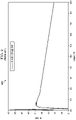
- FIG. 7 is a graph 700 of phase noise at the oscillator outputs (e.g., the output of an output buffer for the related oscillator) as a function of tail inductance Ldegen (e.g., L1) in accordance with an example embodiment.
- Ldegen e.g., L1
- the graph 700 indicates an optimal inductance value for phase alignment between base and emitter signals, leading to improved flicker noise suppression.
- the phase noise is at a minimum when inductance of the tail inductor (Ldegen) is around 800 pH.
- the value of L1 (Ldegen) in an oscillator topology such as the oscillator topologies 300 , 400 , 500 , and 600 is selected to minimize phase noise.
- FIG. 8 is graphs 800 and 810 of voltage as a function of time for transistor terminals (since the active circuit is a symmetric circuit, the graphs 800 and 810 are for the base and emitter voltages of either of Q1 or Q2) of an oscillator topology in accordance with different examples.
- a value of 800 pH is assumed for L1 (Ldegen).
- a value of 200 pH is assumed for L1 (Ldegen).
- FIG. 9 is a graph 900 of phase noise at the oscillator outputs (e.g., the output of an output buffer for the related oscillator) as a function of tail inductance Ldegen (e.g., L1) in accordance with a conventional approach.
- Ldegen e.g., L1
- FIG. 9 indicates the lowest phase noise performance is above ⁇ 61 dBc/Hz, which is approximately 4 dB worse than phase noise performance of the described oscillator topologies (e.g., the oscillator topologies 300 , 500 , and 600 ).
- Couple is used throughout the specification. The term may cover connections, communications, or signal paths that enable a functional relationship consistent with the description of the present disclosure. For example, if device A generates a signal to control device B to perform an action, in a first example device A is coupled to device B, or in a second example device A is coupled to device B through intervening component C if intervening component C does not substantially alter the functional relationship between device A and device B such that device B is controlled by device A via the control signal generated by device A.
- terminal As used herein, the terms “terminal”, “node”, “interconnection”, “pin” are used interchangeably. Unless specifically stated to the contrary, these terms are generally used to mean an interconnection between or a terminus of a device element, a circuit element, an integrated circuit, a device or other electronics or semiconductor component.
- BJTs NPN bipolar junction transistors
- PNP BJTs PNP bipolar junction transistors
- nMOSFET n-channel metal-oxide-silicon field-effect transistors
- MOSFET p-channel MOSFETs
- a current terminal such terminal may be an emitter, collector, source or drain.
- the control terminal may be a base or a gate.
- the diodes of the example embodiments may include any type of diode or diode-connected transistors.
Landscapes
- Physics & Mathematics (AREA)
- Acoustics & Sound (AREA)
- Inductance-Capacitance Distribution Constants And Capacitance-Resistance Oscillators (AREA)
Abstract
An oscillator includes: a bulk-acoustic wave (BAW) resonator having a first BAW resonator terminal and a second BAW resonator terminal; and an active circuit coupled to the first and second BAW resonator terminals and having a series resonance topology with: a first transistor; a second transistor; a first resistor; a second resistor; a capacitive network coupled to first and second BAW resonator terminals and to respective current terminals of the first and second transistors; and an inductor having a first inductor terminal and a second inductor terminal, the first inductor terminal coupled to the capacitive network, and the second inductor terminal coupled to ground terminal.
Description
As new electronic devices are developed and integrated circuit (“IC”) technology advances, new IC products are commercialized. One example IC product for electronic devices is an oscillator. A conventional oscillator circuit generates signal(s) with different resonant frequencies. In addition to including one or more inductors and capacitors, conventional oscillators include a power supply and active circuit to replenish energy due to losses in the oscillator circuit. Different oscillator circuits vary with regard to topology, power consumption, resonant frequencies, quality factor, phase noise, and other parameters. One type of oscillator includes a bulk-acoustic wave (BAW) resonator or microelectromechanical system (MEMS) resonator coupled to an active circuit. Flicker noise (such as, 1/f noise and colored noise) in active devices used in voltage controller oscillators gets up-converted around the oscillation frequency thereby degrading close-in phase noise. This is particularly an issue for close-in frequency offsets (e.g., 1 Hz, 10 Hz, 100 Hz).
In at least one example, an oscillator comprises: a bulk-acoustic wave (BAW) resonator having a first BAW resonator terminal and a second BAW resonator terminal; and an active circuit coupled to the first and second BAW resonator terminals and having a series resonance topology. The series resonance topology includes: a first transistor having a first current terminal, a second current terminal and a first control terminal, the first current terminal coupled to a voltage supply terminal, and the control terminal coupled to the first BAW resonator terminal; a second transistor having a third current terminal, a fourth current terminal and a second control terminal, the third current terminal coupled to the voltage supply terminal, and the second control terminal coupled to the second BAW resonator terminal; a first resistor having a first resistor terminal and a second resistor terminal, the first resistor terminal coupled to the second current terminal, and the second resistor terminal coupled to a ground terminal; a second resistor a third resistor terminal and a fourth resistor terminal, the third resistor terminal coupled to the fourth current terminal, and the fourth resistor terminal coupled to the ground terminal; a capacitive network coupled to the first and second BAW resonator terminals, the second current terminal, and the fourth current terminal; and an inductor having a first inductor terminal and a second inductor terminal, the first inductor terminal coupled to the capacitive network, and the second inductor terminal coupled to ground terminal.
In another example, a system comprises circuitry having a clock input; and an oscillator having a clock output coupled to the clock input of the circuitry. The oscillator has: a BAW resonator having a first BAW resonator terminal and a second BAW resonator terminal; and an active circuit coupled to the first and second BAW resonator terminals and having a series resonance topology. The series resonance topology includes: a first transistor having a first current terminal, a second current terminal and a first control terminal, the first current terminal coupled to a voltage supply terminal, and the control terminal coupled to the first BAW resonator terminal; a second transistor having a third current terminal, a fourth current terminal and a second control terminal, the third current terminal coupled to the voltage supply terminal, and the second control terminal coupled to the second BAW resonator terminal; a first resistor having a first resistor terminal and a second resistor terminal, the first resistor terminal coupled to the second current terminal, and the second resistor terminal coupled to a ground terminal; a second resistor a third resistor terminal and a fourth resistor terminal, the third resistor terminal coupled to the fourth current terminal, and the fourth resistor terminal coupled to the ground terminal; a capacitive network coupled to the first and second BAW resonator terminals, the second current terminal, and the fourth current terminal; and an inductor having a first inductor terminal and a second inductor terminal, the first inductor terminal coupled to the capacitive network, and the second inductor terminal coupled to ground terminal.
The same reference numbers are used in the drawings to depict the same or similar features.
In this description, an oscillator includes a bulk-acoustic wave (BAW) resonator and an active circuit with features to deliver ultra-flow flicker noise performance at close-in frequency offsets (e.g., 10 Hz, 100 Hz, and 1 kHz). With ultra-flow flicker noise performance at close-in frequency offsets, the phase noise of the oscillator is reduced, which is an important performance metric for seismic clocks, atomic clocks, or other time references for use with a Global System for Mobile Communications (GSM) satellite or other applications that rely on long term stability, low drift time references. As used herein, “close-in frequency offsets” refers to sub parts-per-million (ppm) offsets. For example, at 2.5 GHz, offsets below 2.5 kHz are close-in frequency offsets.
In some example embodiments, the active circuit includes a bipolar junction transistor (BJT)-based differential series topology with large devices to limit series capacitive reactance and lower inherent flicker. In some example embodiments, the device size is selected to be as large as possible subject to constraints such as power consumption, area overhead, distributed impedance targets, or other practical constraints. In some example embodiments, the active circuit includes split inductive and resistive degeneration, for flicker suppression and suppression through fine phase alignment between base and emitter voltages. In some example embodiments, the active circuit includes a large common-mode direct-current (DC) biasing inductor, which allows for a single common signal electrostatic discharge (ESD) between transistor base terminals without affecting the oscillation frequency.
In some example embodiments, the equivalent circuit used to model the BAW resonator 108 in FIG. 1 has the following characteristics:
The effective inductance, Leff, expression is used here to explain the concept behind using the BAW resonator in an oscillator. Between the series and the parallel resonance frequencies (the series resonance frequency being lower in frequency than the parallel resonance frequency), the BAW resonator behaves like an inductor. To exploit the series resonance of the BAW resonator in an oscillator, the size of active circuit components (e.g., transistors and metal capacitors) are selected to keep the oscillation frequency as close to the natural series resonance of the BAW resonator as possible since the quality factor of the BAW resonator degrades as one moves away from the natural series resonance. The size of active circuit components is subject to power and area constraints. For example, an active circuit with a very large capacitor will have a distributed inductance which will push the self-resonance frequency (SRF) of the capacitor close to the oscillator frequency, which can lead to design failure. In some example embodiments, capacitor sizes for the active circuit is selected so that the SRF of each capacitor falls below 5*fosc, where fosc is the oscillation frequency (e.g., 2.5 GHz). The size of transistors for the active circuit is subject to “negative resistance” constraints
used by the active circuit to compensate for the losses in the BAW resonator. This is an iterative process since the transistors will also contribute to the base emitter capacitance in addition to the capacitor added between the base and the emitter.
In some example embodiments, the active circuit 104 may be designed to efficiently compensate for the expected losses of the BAW resonator 108 without negatively affecting desired parameters (such as quality factor) and/or with minimal degradation of parameters such as phase noise or jitter. For the oscillator 102, the combination of the BAW resonator 108 and the active circuit 104 determine the resonant frequencies. For example, the active circuit 104 may couple to the BAW resonator 108 in series or in parallel (shunt) depending on the oscillator topology.
In some example embodiments, the active circuit 104 provides a clocking signal with ultra-low flicker noise performance at close-in frequency offsets (e.g., 10 Hz, 100 Hz, 1 kHz). In the example of FIG. 1 , the features include a series resonance topology 106 with: 1) BJTs sized to maximize series capacitance; 2) split common-mode (CM) resonance (e.g., use of a split inductive and resistive degeneration); 3) ESD-compliant bias circuit; 4) the BJTs are R-degeneration NPN devices for improved flicker performance; and 5) a figure eight shape tail inductor for reduced coupling. In other example embodiments, the features of the active circuit 104 may vary. Regarding the first feature (BJTs sized to maximize series capacitance), the BJT size should minimize the series reactance looking into the base terminals. In some example embodiments, selecting the size of the BJT is an iterative process that involves selecting the largest capacitor size for the active circuit that can implemented practically such that the SRF of the capacitors are above a threshold (e.g., 5*fosc). Next, the effective series resistance (reff, or “effective losses”) of the BAW resonator is calculated based on the effective frequency of oscillation given by the resonance frequency of the equivalent BAW inductor (Leff) and the previously selected capacitors for the active circuit (whose SRF is above the threshold). Iteration of BJT sizes that satisfy
is then performed. This is an iterative process since there will be a set of BJT sizes (with variance in length and/or width) that satisfy this constraint. Additionally, each BJT option will add its own intrinsic capacitance between the base emitter junction in addition to the metal capacitors that were selected. The selected BJT size will be dictated by target criteria such as a target phase noise at a given frequency offset. If there are multiple BJT options still available, the most power/area optimal solution may be selected.
This allows the BAW resonator 108 to operate close to its natural series resonance where it exhibits the maximum Q (quality factor). In other words, as the size of the BJT increases, the frequency pulling experienced by the BAW resonator 108 decreases, resulting in a higher Q and lower phase noise. Regarding the fifth feature (a figure eight shape tail inductor), any magnetically isolated shape (e.g., clover shaped inductors) would also work.
In conventional topologies, the inductive degeneration is common to all nodes in an active circuit and is explicitly tuned to the 2nd harmonic of the oscillation frequency. In contrast, in the topology of the example embodiments, the DC path is degenerated through a resistor while the frequency determining the alternating current (AC) path is degenerated at a common mode node through an inductor. Accordingly, the CM degeneration inductor does not resonate at the 2nd harmonic. Instead, the CM degeneration inductor is used to attain fine phase alignment between emitter and base voltages.
In some example embodiments, the oscillator 102 with the BAW resonator 108 and the active circuit 104 is a type of Clapp or Colpitts oscillator. In some example embodiments, the series resonance topology 106 includes a DC only CM biasing inductor/choke that allows for a single signal ESD for two transistor base terminals. In conventional MEMS series oscillators, the base terminals are resistively biased which adds noise and parasitic shunt loading at the oscillation frequency. In one conventional approach, the inductor whose center tap is used to bias the transistor base terminals is also the primary frequency determining element (oscillating element). In another conventional approach, a microelectromechanical system (MEMS)-based resonator uses the MEMS device as the primary resonance elements and MEMS devices are DC open and thus cannot be used for biasing.
In contrast, in the described topology, an inductor is used as the bias element, which allows a low resistance DC path. Also, the inductor is sized to self-resonate at the oscillation frequency to minimize shunt parasitics. For the oscillator 102, this DC biasing inductor of the active circuit 104 has high-impedance (approaching an open circuit) at the oscillation frequency, thereby having no impact on the oscillation frequency. Additionally, the center tap of the active circuit 104 is connected to a single signal ESD that serves to provide a discharge path through the inductor and ESD protection at any of the two bases to which the BAW resonator 108 is connected. Having a common signal ESD for the active circuit 104 lowers the overall non-linear capacitance connected to the signal nodes in addition to making the active circuit 104 common mode, both of which serve to lower its impact on the flicker performance of the oscillator 102.
In some example embodiments, a transistor collector terminal of the active circuit 104 is used as a common mode node (AC ground) tied to a voltage supply (VDD) Also, the output is tapped directly from the base node (to which the BAW resonator 108 is directly connected). With large devices, the series capacitive reactance associated with the active circuit 104 is lowered, which allows for tapping the signal directly from a transistor base terminal without affecting performance through loading. In contrast, conventional approaches tap the output either from the transistor collector terminal or the transistor emitter terminal.
In some example embodiments, split CM degeneration is used for fine phase alignment between base and emitter terminal voltages as opposed to a basic 2nd harmonic resonance. This leads to a superior close-in phase noise improvement (>3 dB) over a common degeneration inductor as done in conventional approaches. Split CM degeneration also provides an additional degree of freedom in the active circuit 104 as the degeneration resistance and inductor sizing expand the potential solution set for optimal performance.
In some example embodiments, use of a DC CM biasing inductor and ESD protection circuitry for the active circuit 104 helps lower the nonlinear capacitance through ESD protection circuitry as well as making the load presented to the circuit by the ESD a common mode load. Use of a DC CM biasing inductor and ESD protection circuitry for the active circuit 104 also allows for ESD compliance without sacrificing any flicker performance due to the non-linear (signal dependent) ESD capacitance. In some example embodiments, the active circuit 104 uses: split inductive and resistive degeneration; DC biasing CM inductor (choke) with a single common ESD; and lower flicker from inherently large BJTs (to limit series capacitive reactance).
In the example of FIG. 3 , Q1 has a first current terminal (e.g., collector of Q1), a second current terminal (e.g., emitter of Q1) and a first control terminal (e.g., base of Q1), the first current terminal coupled to the voltage supply terminal 302, and the control terminal coupled to a first terminal of the BAW resonator 310. Also, Q2 has a third current terminal (e.g., collector of Q2), a fourth current terminal (e.g., emitter of Q2) and a second control terminal (e.g., base of Q2), the third current terminal coupled to the voltage supply terminal 302, and the second control terminal coupled to a second terminal of the BAW resonator 310. In addition, R1 has a first resistor terminal and a second resistor terminal. The first resistor terminal of R1 coupled to the second current terminal, and the second resistor terminal of R1 coupled to a ground terminal 306. R2 has a third resistor terminal and a fourth resistor terminal. The third resistor terminal of R2 coupled to the fourth current terminal, and the fourth resistor terminal of R2 coupled to the ground terminal 306.
As shown, the capacitive network includes a first network terminal (at a first/top terminal of C1) coupled to the first terminal of the BAW resonator 310. The capacitive network also includes a second network terminal (at a second/bottom terminal of C1 and a first/top terminal of C2) coupled to the second current terminal (e.g., the emitter of Q1). The capacitive network further includes a third network terminal (at a second/bottom terminal of C2) coupled to a first inductor terminal (at a first/top terminal of L1). The capacitive network further includes a fourth network terminal (at a first/top terminal of C3) coupled to the second terminal of the BAW resonator 310. The capacitor network also includes a fifth network terminal (at a second/bottom terminal of C3 and at a first/top terminal of C4) coupled to the fourth current terminal (e.g., the emitter of Q1). Moreover, the capacitive network includes a sixth network terminal (at a second/bottom terminal of C4) coupled to the first inductor terminal (at the first/top terminal of L1). In some example embodiments, the capacitive network includes: a first capacitor (e.g., C1) coupled between the first and second network terminals; a second capacitor (e.g., C2) coupled between the second and third network terminals; a third capacitor C3) coupled between the fourth and fifth network terminals; and a fourth capacitor (C4) coupled between the fifth and sixth network terminals.
In some example embodiments, L2 of the oscillator topology 300 has a third inductor terminal (at a first/left terminal of L2) and a fourth inductor terminal (at a second/right terminal of L2. The third inductor terminal is coupled to the first terminal BAW resonator 310, and the fourth inductor terminal is coupled to a bias terminal 304. In some example embodiments, L3 of the oscillator topology 300 has a fifth inductor terminal (at a first/right terminal of L3) and a sixth inductor terminal (at a second/left terminal of L3). The fifth inductor terminal is coupled to the second terminal the BAW resonator 310, and the sixth inductor terminal is coupled to the bias terminal 304.
In some example embodiments, a bias circuit (e.g., RDAC 502 in FIG. 5 ) is coupled to the bias terminal 304 and is configured to provide a direct current bias to the bias terminal 304. Also, ESD protection circuitry may be coupled to the bias terminal 304. In some example embodiments, the ESD protection circuitry includes a first diode (e.g., D1 in FIG. 3 ) having a first anode and a first cathode. The first anode is coupled to the bias terminal 304, and the first cathode coupled to the voltage supply terminal 302. The ESD protection circuitry also includes a second diode (e.g., D2) having a second anode and a second cathode. The second cathode is coupled to the bias terminal 304, and the second anode is coupled to the common voltage potential (e.g. ground terminal) 306.
In the oscillator topology 400, resistor R3 replaces L2, and resistor R4 replaces L3. Specifically R3 has a fifth resistor terminal and a sixth resistor terminal. The fifth resistor terminal is coupled to the first BAW resonator terminal, and the sixth resistor terminal is coupled to a bias terminal. Also, R4 has a seventh resistor terminal and an eighth resistor terminal. The seventh resistor terminal is coupled to the second BAW resonator terminal, and the eighth resistor terminal is coupled to the bias terminal.
Also, the oscillator topology 400 includes ESD protection circuitry at the control (base) terminals of Q1 and Q2. The ESD protection circuitry of the oscillator topology 400 includes the diodes D3 and D4. As shown, D3 includes a cathode coupled to the control terminal of Q1, and an anode coupled to the ground 306. D4 includes a cathode coupled to the control terminal of Q2, and an anode coupled to the ground 306.
In some example embodiments, D3 and D4 are base-collector (BC) junctions to prevent against positive ESD events (spikes) through the BC pn junctions. In such case, a path is provided only for negative ESD events. For the oscillator topology 400, Q1 and Q2 cannot be used to effectively counter ESD events due to emitter degeneration resistance limiting the conductivity. By design, Q1 and Q2 are much bigger than a diode size required to support machine model (MM) ESD events (MM ESD events emulate ESD events caused by automated machine handling of ICs), thereby allowing for absorption of the relatively small non-linear ESD capacitance. In some example embodiments, the size of the ESD is emulated as the smallest diode size that satisfies the charge/discharge criterion for a machine model event. It varies slightly from one technology node to the other, but this diode size has no correlation to the actual BJT size in the oscillator. Likewise, the ESD capacitance will depend on the size of the ESD diode (again, not controlled by the designer).
In the oscillator topology 500, example structures for C1-C4 and L1-L3 are given. More specifically, L1 has a figure eight shape, L2 has a C shape, and L3 has a reverse C shape. Also, in some example embodiments, each of C1-C4 are metal-oxide metal (MOM) capacitators (sometimes referred to as finger caps). In the example of FIG. 5 , the BAW resonator 310A is coupled to a bias circuit 502 (e.g., a 7-bit resistive digital-to-analog converter or RDAC). The bias circuit 502 includes resistors R5-R7 and a capacitor C5 in the arrangement shown with R7 and R6 in series between the voltage supply terminal 302 and the ground terminal 306. As shown, R7 is a variable resistor in FIG. 5 . Also, R5 is coupled between the BAW resonator 310A and the connection between R6 and R7. Further, C5 is coupled between the ground node 306 and the connection between R7 and R6.
Also, the oscillator topology 500 includes ESD protection circuitry coupled to the BAW resonator 310A. The ESD protection circuitry of the oscillator topology 500 includes the diodes D5 and D6. As shown, D5 includes a cathode coupled to the voltage supply terminal 302, and an anode coupled to the BAW resonator 310A. D6 includes a cathode coupled to the BAW resonator 310A, and an anode coupled to the ground terminal 306.
The oscillator topology 500 includes various features to improve phase noise performance at close-in offsets. The features include: a split-CM resonance (L2 and L3); an ESD-compliant (due to D1 and D2) CM inductive bias (the 7-bit RDAC 502 coupled to D1 and D2); R-degeneration NPNs (Q1 and Q2) for improved flicker performance; and a figure eight shape tail inductor (L1) for reduced coupling. In some example embodiments, the bias can be brought in through an resistive DAC (RDAC), or a current DAC (IDAC) pumping current directly into the base terminal or by pumping current into a diode-connected MOSFET. There are many possible ways to provide the bias, and the described topologies are compatible with all such biasing schemes.
In the oscillator topology 600, the BAW resonator 310 and C1-C4 are identified as frequency determining elements 614. Also, the signal pads 615 and 616 coupled to the terminals of the BAW resonator 310 are ESD protected by ESD protection circuitry 612 coupled to the bias terminal 304. The ESD protection circuitry 612 includes D1 and D2 in the same arrangement described for FIG. 3 . In the example of FIG. 6 , a voltage DAC 610 is used as a DC bias source 608. In some example embodiments, voltage DAC 610 does not affect the oscillation frequency. The frequency is determined by C1-C4 and BAW 310.
As shown, the oscillator topology 600 also includes supply protection circuitry 602 with a resistor-capacitor (RC) clamp 604 and ESD protection circuitry including diodes D5 and D6. More specifically, the cathode of D5 is coupled to a second voltage supply (I/O VDD) terminal 620, and the anode of D5 is coupled to the voltage supply terminal 302. Also, the cathode of D6 is coupled to the voltage supply terminal 302, and the anode of D6 is coupled to the ground terminal 306.
With the oscillator topology 600, a CM inductor (L2 or L3) is driven by the voltage DAC 610 for DC biasing only (without affecting the oscillation frequency). Also, the CM inductor (L2 or L3) provides a common ESD path for the signal pads 615 and 616 coupled to terminals of the BAW resonator 310 and the control terminals of Q1 and Q2 (NPN BJTs).
With the oscillator topologies 300, 400, 500, and 600, close-in (flicker region) phase noise performance of an oscillator with BAW resonator is improved through a combination of device degeneration and tail filtering. In some example embodiments, ESD compliance may be achieved, without any performance penalty, through inductive base biasing as described for oscillator topologies 300, 500, and 600 of FIGS. 3, 5, and 6 . The CM biasing inductor should be as large as possible and can operate beyond its self-resonant frequency (SRF) at the frequency of interest since its only for DC biasing and should present as high an impedance as possible at the oscillation frequency. The tail inductor (L1 in the oscillator topologies 300, 400, 500, and 600) is used for fine phase alignment between the base and the collector voltages. The tail inductor differs from a regular choke or 2nd harmonic inductor since its always shunted by the small emitter degeneration resistor (R1 or R2 in the oscillator topologies 300, 400, 500, and 600). With the tail inductor (L1, also referred to as Ldegen herein), the oscillator topologies 300, 400, 500, and 600 are also less sensitive to ground parasitic inductance compared to other oscillator topologies.
The term “couple” is used throughout the specification. The term may cover connections, communications, or signal paths that enable a functional relationship consistent with the description of the present disclosure. For example, if device A generates a signal to control device B to perform an action, in a first example device A is coupled to device B, or in a second example device A is coupled to device B through intervening component C if intervening component C does not substantially alter the functional relationship between device A and device B such that device B is controlled by device A via the control signal generated by device A.
As used herein, the terms “terminal”, “node”, “interconnection”, “pin” are used interchangeably. Unless specifically stated to the contrary, these terms are generally used to mean an interconnection between or a terminus of a device element, a circuit element, an integrated circuit, a device or other electronics or semiconductor component.
While the example embodiments above utilize NPN bipolar junction transistors (BJTs), other example embodiments may utilize PNP BJTs, n-channel metal-oxide-silicon field-effect transistors (nMOSFET), p-channel MOSFETs or any other type of transistor. Hence, when referring to a current terminal, such terminal may be an emitter, collector, source or drain. In addition, the control terminal may be a base or a gate. In addition, the diodes of the example embodiments may include any type of diode or diode-connected transistors.
Modifications are possible in the described embodiments, and other embodiments are possible, within the scope of the claims.
Claims (20)
1. An oscillator, comprising:
a bulk-acoustic wave (BAW) resonator having a first BAW resonator terminal and a second BAW resonator terminal;
an active circuit coupled to the first and second BAW resonator terminals and having a series resonance topology with:
a first transistor having a first current terminal, a second current terminal and a first control terminal, the first current terminal coupled to a voltage supply terminal, and the first control terminal coupled to the first BAW resonator terminal;
a second transistor having a third current terminal, a fourth current terminal and a second control terminal, the third current terminal coupled to the voltage supply terminal, and the second control terminal coupled to the second BAW resonator terminal;
a first resistor having a first resistor terminal and a second resistor terminal, the first resistor terminal coupled to the second current terminal, and the second resistor terminal coupled to a ground terminal;
a second resistor having a third resistor terminal and a fourth resistor terminal, the third resistor terminal coupled to the fourth current terminal, and the fourth resistor terminal coupled to the ground terminal;
a capacitive network coupled to the first and second BAW resonator terminals, the second current terminal, and the fourth current terminal; and
an inductor having a first inductor terminal and a second inductor terminal, the first inductor terminal coupled to the capacitive network, and the second inductor terminal coupled to the ground terminal; and
an inductive bias network coupled to the first and second BAW resonator terminals and to the first and second control terminals.
2. The oscillator of claim 1 , wherein the capacitive network includes a first network terminal, a second network terminal, a third network terminal, a fourth network terminal, and a fifth network terminal, the first network terminal coupled to the first BAW resonator terminal, the second network terminal coupled to the second current terminal, the third network terminal coupled to the first inductor terminal, the fourth network terminal coupled to the second BAW resonator terminal, and the fifth network terminal coupled to the fourth current terminal.
3. The oscillator of claim 2 , wherein the capacitive network includes:
a first capacitor coupled between the first and second network terminals;
a second capacitor coupled between the second and third network terminals;
a third capacitor coupled between the fourth and fifth network terminals; and
a fourth capacitor coupled between the fifth and third network terminals.
4. The oscillator of claim 1 , wherein the inductor is a first inductor, and the inductive bias network comprises:
a second inductor having a third inductor terminal and a fourth inductor terminal, the third inductor terminal coupled to the first BAW resonator terminal, and the fourth inductor terminal coupled to a bias terminal; and
a third inductor having a fifth inductor terminal and a sixth inductor terminal, the fifth inductor terminal coupled to the second BAW resonator terminal, and the sixth inductor terminal coupled to the bias terminal.
5. The oscillator of claim 4 , further comprising:
a bias circuit coupled to the bias terminal and configured to provide a direct current bias to the bias terminal; and
electrostatic discharge (ESD) protection circuitry coupled to the bias terminal.
6. The oscillator of claim 5 , wherein the ESD protection circuitry includes:
a first diode having a first anode and a first cathode, the first anode coupled to the bias terminal, and the first cathode coupled to voltage supply terminal; and
a second diode having a second anode and a second cathode, the second cathode coupled to the bias terminal, and the second anode coupled to the ground terminal.
7. The oscillator of claim 1 , wherein the first and second transistors are NPN bipolar junction transistors and the active circuit includes:
a split common-mode (CM) resonance; and
an electrostatic discharge (ESD) protected common-mode inductive bias.
8. The oscillator of claim 1 , wherein the inductor has a figure eight shape.
9. The oscillator of claim 1 , further comprising:
a voltage supply protection circuit coupled to the voltage supply terminal; and
a clamp circuit coupled between the voltage supply terminal and the ground terminal.
10. A system, comprising:
circuitry having a clock input; and
an oscillator having a clock output coupled to the clock input of the circuitry, the oscillator having:
a bulk-acoustic wave (BAW) resonator having a first BAW resonator terminal and a second BAW resonator terminal;
an active circuit coupled to the first and second BAW resonator terminals and having a series resonance topology with:
a first transistor having a first current terminal, a second current terminal and a first control terminal, the first current terminal coupled to a voltage supply terminal, and the control terminal coupled to the first BAW resonator terminal;
a second transistor having a third current terminal, a fourth current terminal and a second control terminal, the third current terminal coupled to the voltage supply terminal, and the second control terminal coupled to the second BAW resonator terminal;
a first resistor having a first resistor terminal and a second resistor terminal, the first resistor terminal coupled to the second current terminal, and the second resistor terminal coupled to a ground terminal;
a second resistor having a third resistor terminal and a fourth resistor terminal, the third resistor terminal coupled to the fourth current terminal, and the fourth resistor terminal coupled to the ground terminal;
a capacitive network coupled to the first and second BAW resonator terminals, the second current terminal, and the fourth current terminal; and
an inductor having a first inductor terminal and a second inductor terminal, the first inductor terminal coupled to the capacitive network, and the second inductor terminal coupled to ground terminal; and
an inductive bias network coupled to the first and second BAW resonator terminals and to the first and second control terminals.
11. The system of claim 10 , wherein the capacitive network includes a first network terminal, a second network terminal, a third network terminal, a fourth network terminal, and a fifth network terminal, the first network terminal coupled to the first BAW resonator terminal, the second network terminal coupled to the second current terminal, the third network terminal coupled to the first inductor terminal, the fourth network terminal coupled to the second BAW resonator terminal, and the fifth network terminal coupled to the fourth current terminal.
12. The system of claim 11 , wherein the capacitive network includes:
a first capacitor coupled between the first and second network terminals;
a second capacitor coupled between the second and third network terminals;
a third capacitor coupled between the fourth and fifth network terminals; and
a fourth capacitor coupled between the fifth and third network terminals.
13. The system of claim 10 , wherein the inductor is a first inductor, and the inductive bias network includes:
a second inductor having a third inductor terminal and a fourth inductor terminal, the third inductor terminal coupled to the first BAW resonator terminal, and the fourth inductor terminal coupled to a bias terminal; and
a third inductor having a fifth inductor terminal and a sixth inductor terminal, the fifth inductor terminal coupled to the second BAW resonator terminal, and the sixth inductor terminal coupled to the bias terminal.
14. The system of claim 13 , further comprising:
a bias circuit coupled to the bias terminal and configured to provide a direct current bias to the bias terminal; and
electrostatic discharge (ESD) protection circuitry coupled to the bias terminal.
15. The system of claim 10 , wherein the first and second transistors are NPN bipolar junction transistors (BJTs), and the active circuit includes:
a split common-mode (CM) resonance; and
an electrostatic discharge (ESD) protected common-mode inductive bias.
16. The system of claim 10 , wherein the inductor has a figure eight shape.
17. The system of claim 10 , wherein the oscillator is implemented on a single semiconductor die.
18. An oscillator, comprising:
a bulk-acoustic wave (BAW) resonator having a first BAW resonator terminal and a second BAW resonator terminal;
an active circuit coupled to the first and second BAW resonator terminals and having a series resonance topology with:
a first transistor having a first current terminal, a second current terminal and a first control terminal, the first current terminal coupled to a voltage supply terminal, and the first control terminal coupled to the first BAW resonator terminal;
a second transistor having a third current terminal, a fourth current terminal and a second control terminal, the third current terminal coupled to the voltage supply terminal, and the second control terminal coupled to the second BAW resonator terminal;
a first resistor having a first resistor terminal and a second resistor terminal, the first resistor terminal coupled to the second current terminal, and the second resistor terminal coupled to a ground terminal;
a second resistor having a third resistor terminal and a fourth resistor terminal, the third resistor terminal coupled to the fourth current terminal, and the fourth resistor terminal coupled to the ground terminal;
a capacitive network coupled to the first and second BAW resonator terminals, the second current terminal, and the fourth current terminal; and
an inductor having a first inductor terminal and a second inductor terminal, the first inductor terminal coupled to the capacitive network, and the second inductor terminal coupled to the ground terminal; and
a resistive bias network coupled to the first and second BAW resonator terminals, to the first and second control terminals and to a bias terminal.
19. The oscillator of claim 18 , wherein the resistive bias network includes:
a third resistor having a fifth resistor terminal and a sixth resistor terminal, the fifth resistor terminal coupled to the first BAW resonator terminal, and the sixth resistor terminal coupled to the bias terminal; and
a fourth resistor having a seventh resistor terminal and an eighth resistor terminal, the seventh resistor terminal coupled to the second BAW resonator terminal, and the eighth resistor terminal coupled to the bias terminal.
20. The oscillator of claim 18 , further comprising:
first and second diodes, the first diode having a first cathode coupled to the first BAW resonator terminal and a first anode coupled to the ground terminal, and the second diode having a second cathode coupled to the second BAW resonator terminal and a second anode coupled to the ground terminal.
Priority Applications (2)
| Application Number | Priority Date | Filing Date | Title |
|---|---|---|---|
| US17/189,556 US11368124B1 (en) | 2021-03-02 | 2021-03-02 | Oscillator with bulk-acoustic wave (BAW) resonator and series-resonance topology |
| CN202210170354.5A CN115001435A (en) | 2021-03-02 | 2022-02-24 | Oscillator with Bulk Acoustic Wave (BAW) resonator and series resonant topology |
Applications Claiming Priority (1)
| Application Number | Priority Date | Filing Date | Title |
|---|---|---|---|
| US17/189,556 US11368124B1 (en) | 2021-03-02 | 2021-03-02 | Oscillator with bulk-acoustic wave (BAW) resonator and series-resonance topology |
Publications (1)
| Publication Number | Publication Date |
|---|---|
| US11368124B1 true US11368124B1 (en) | 2022-06-21 |
Family
ID=82060497
Family Applications (1)
| Application Number | Title | Priority Date | Filing Date |
|---|---|---|---|
| US17/189,556 Active US11368124B1 (en) | 2021-03-02 | 2021-03-02 | Oscillator with bulk-acoustic wave (BAW) resonator and series-resonance topology |
Country Status (2)
| Country | Link |
|---|---|
| US (1) | US11368124B1 (en) |
| CN (1) | CN115001435A (en) |
Cited By (1)
| Publication number | Priority date | Publication date | Assignee | Title |
|---|---|---|---|---|
| CN117353730A (en) * | 2023-11-02 | 2024-01-05 | 西安电子科技大学 | A capacitor and inductor based on topological insulators |
Families Citing this family (1)
| Publication number | Priority date | Publication date | Assignee | Title |
|---|---|---|---|---|
| CN121461972B (en) * | 2025-10-21 | 2026-04-17 | 北京炬力北方微电子股份有限公司 | Method for reducing CDR recovered clock and data jitter and digital-to-analog converter thereof |
Citations (2)
| Publication number | Priority date | Publication date | Assignee | Title |
|---|---|---|---|---|
| US7002423B1 (en) * | 2004-07-20 | 2006-02-21 | Pericom Semiconductor Corp. | Crystal clock generator operating at third overtone of crystal's fundamental frequency |
| US20110018649A1 (en) * | 2008-01-18 | 2011-01-27 | Commissar.A L'energ.Atom.Et Aux Energ. Altern. | Electrical resonator device with a wide frequency variation range |
-
2021
- 2021-03-02 US US17/189,556 patent/US11368124B1/en active Active
-
2022
- 2022-02-24 CN CN202210170354.5A patent/CN115001435A/en active Pending
Patent Citations (2)
| Publication number | Priority date | Publication date | Assignee | Title |
|---|---|---|---|---|
| US7002423B1 (en) * | 2004-07-20 | 2006-02-21 | Pericom Semiconductor Corp. | Crystal clock generator operating at third overtone of crystal's fundamental frequency |
| US20110018649A1 (en) * | 2008-01-18 | 2011-01-27 | Commissar.A L'energ.Atom.Et Aux Energ. Altern. | Electrical resonator device with a wide frequency variation range |
Cited By (1)
| Publication number | Priority date | Publication date | Assignee | Title |
|---|---|---|---|---|
| CN117353730A (en) * | 2023-11-02 | 2024-01-05 | 西安电子科技大学 | A capacitor and inductor based on topological insulators |
Also Published As
| Publication number | Publication date |
|---|---|
| CN115001435A (en) | 2022-09-02 |
Similar Documents
| Publication | Publication Date | Title |
|---|---|---|
| US7321271B2 (en) | Voltage-controlled oscillator, radio communication apparatus and voltage-controlled oscillation method for reducing degradation of phase noise characteristic | |
| Rogers et al. | The effect of varactor nonlinearity on the phase noise of completely integrated VCOs | |
| JP2007300623A (en) | Oscillation circuit with embedded power supply circuit | |
| US11228280B1 (en) | Microelectromechanical system resonator-based oscillator | |
| JP4067664B2 (en) | Wide frequency range and low noise voltage controlled oscillator for integrated circuit configurations | |
| US20050156681A1 (en) | Voltage controlled oscillator | |
| US11368124B1 (en) | Oscillator with bulk-acoustic wave (BAW) resonator and series-resonance topology | |
| US6469586B1 (en) | Low voltage voltage-controlled oscillator topology | |
| US20070085620A1 (en) | Semiconductor integrated circuit device | |
| US8222963B2 (en) | Voltage-controlled oscillator | |
| US7057469B2 (en) | High speed differential voltage controlled oscillator | |
| KR100938086B1 (en) | oscillator | |
| US20060220754A1 (en) | Voltage controlled oscillator | |
| CN1671051B (en) | Low Phase Noise Switched Capacitor Circuits and Related Methods for Suppressing Clock Feedthrough Effect | |
| CN102163968B (en) | Integrated circuit with LC tank circuit and method of operation thereof | |
| US7385452B2 (en) | Voltage controlled oscillator using capacitive degeneration | |
| US6724273B1 (en) | Filter circuitry for voltage controlled oscillator | |
| Samori et al. | Integrated LC oscillators for frequency synthesis in wireless applications | |
| US11239795B2 (en) | Fully integrated oscillator for ultra low voltage applications with quadrupled voltage and low phase noise | |
| US6952140B2 (en) | Ocillator and electronic device using same | |
| CN111162736B (en) | Voltage controlled oscillator | |
| US7193483B2 (en) | Blocking a leakage current | |
| US7170355B2 (en) | Voltage-controlled oscillator using current feedback network | |
| JP2003324315A (en) | Voltage controlled oscillator | |
| JP4677696B2 (en) | Balanced oscillation circuit and electronic device using the same |
Legal Events
| Date | Code | Title | Description |
|---|---|---|---|
| FEPP | Fee payment procedure |
Free format text: ENTITY STATUS SET TO UNDISCOUNTED (ORIGINAL EVENT CODE: BIG.); ENTITY STATUS OF PATENT OWNER: LARGE ENTITY |
|
| STCF | Information on status: patent grant |
Free format text: PATENTED CASE |
|
| MAFP | Maintenance fee payment |
Free format text: PAYMENT OF MAINTENANCE FEE, 4TH YEAR, LARGE ENTITY (ORIGINAL EVENT CODE: M1551); ENTITY STATUS OF PATENT OWNER: LARGE ENTITY Year of fee payment: 4 |