US7885683B2 - Method and system for simultaneous FM transmit and FM receive functions using an integrated bluetooth local oscillator generator (LOGEN) - Google Patents
Method and system for simultaneous FM transmit and FM receive functions using an integrated bluetooth local oscillator generator (LOGEN) Download PDFInfo
- Publication number
- US7885683B2 US7885683B2 US11/754,708 US75470807A US7885683B2 US 7885683 B2 US7885683 B2 US 7885683B2 US 75470807 A US75470807 A US 75470807A US 7885683 B2 US7885683 B2 US 7885683B2
- Authority
- US
- United States
- Prior art keywords
- frequency
- ddfs
- signals
- clock signal
- signal
- Prior art date
- Legal status (The legal status is an assumption and is not a legal conclusion. Google has not performed a legal analysis and makes no representation as to the accuracy of the status listed.)
- Active, expires
Links
Images


Classifications
-
- H—ELECTRICITY
- H03—ELECTRONIC CIRCUITRY
- H03F—AMPLIFIERS
- H03F3/00—Amplifiers with only discharge tubes or only semiconductor devices as amplifying elements
- H03F3/20—Power amplifiers, e.g. Class B amplifiers, Class C amplifiers
- H03F3/21—Power amplifiers, e.g. Class B amplifiers, Class C amplifiers with semiconductor devices only
- H03F3/211—Power amplifiers, e.g. Class B amplifiers, Class C amplifiers with semiconductor devices only using a combination of several amplifiers
-
- H—ELECTRICITY
- H03—ELECTRONIC CIRCUITRY
- H03F—AMPLIFIERS
- H03F3/00—Amplifiers with only discharge tubes or only semiconductor devices as amplifying elements
- H03F3/20—Power amplifiers, e.g. Class B amplifiers, Class C amplifiers
- H03F3/24—Power amplifiers, e.g. Class B amplifiers, Class C amplifiers of transmitter output stages
- H03F3/245—Power amplifiers, e.g. Class B amplifiers, Class C amplifiers of transmitter output stages with semiconductor devices only
-
- H—ELECTRICITY
- H03—ELECTRONIC CIRCUITRY
- H03F—AMPLIFIERS
- H03F3/00—Amplifiers with only discharge tubes or only semiconductor devices as amplifying elements
- H03F3/72—Gated amplifiers, i.e. amplifiers which are rendered operative or inoperative by means of a control signal
-
- H—ELECTRICITY
- H03—ELECTRONIC CIRCUITRY
- H03G—CONTROL OF AMPLIFICATION
- H03G3/00—Gain control in amplifiers or frequency changers without distortion of the input signal
- H03G3/20—Automatic control
- H03G3/30—Automatic control in amplifiers having semiconductor devices
- H03G3/3052—Automatic control in amplifiers having semiconductor devices in bandpass amplifiers (H.F. or I.F.) or in frequency-changers used in a (super)heterodyne receiver
- H03G3/3068—Circuits generating control signals for both R.F. and I.F. stages
-
- H—ELECTRICITY
- H03—ELECTRONIC CIRCUITRY
- H03G—CONTROL OF AMPLIFICATION
- H03G3/00—Gain control in amplifiers or frequency changers without distortion of the input signal
- H03G3/20—Automatic control
- H03G3/30—Automatic control in amplifiers having semiconductor devices
- H03G3/3052—Automatic control in amplifiers having semiconductor devices in bandpass amplifiers (H.F. or I.F.) or in frequency-changers used in a (super)heterodyne receiver
- H03G3/3078—Circuits generating control signals for digitally modulated signals
-
- H—ELECTRICITY
- H03—ELECTRONIC CIRCUITRY
- H03F—AMPLIFIERS
- H03F2200/00—Indexing scheme relating to amplifiers
- H03F2200/129—Indexing scheme relating to amplifiers there being a feedback over the complete amplifier
-
- H—ELECTRICITY
- H03—ELECTRONIC CIRCUITRY
- H03F—AMPLIFIERS
- H03F2200/00—Indexing scheme relating to amplifiers
- H03F2200/156—One or more switches are realised in the feedback circuit of the amplifier stage
-
- H—ELECTRICITY
- H03—ELECTRONIC CIRCUITRY
- H03F—AMPLIFIERS
- H03F2200/00—Indexing scheme relating to amplifiers
- H03F2200/294—Indexing scheme relating to amplifiers the amplifier being a low noise amplifier [LNA]
-
- H—ELECTRICITY
- H03—ELECTRONIC CIRCUITRY
- H03F—AMPLIFIERS
- H03F2200/00—Indexing scheme relating to amplifiers
- H03F2200/451—Indexing scheme relating to amplifiers the amplifier being a radio frequency amplifier
-
- H—ELECTRICITY
- H03—ELECTRONIC CIRCUITRY
- H03F—AMPLIFIERS
- H03F2203/00—Indexing scheme relating to amplifiers with only discharge tubes or only semiconductor devices as amplifying elements covered by H03F3/00
- H03F2203/72—Indexing scheme relating to gated amplifiers, i.e. amplifiers which are rendered operative or inoperative by means of a control signal
- H03F2203/7236—Indexing scheme relating to gated amplifiers, i.e. amplifiers which are rendered operative or inoperative by means of a control signal the gated amplifier being switched on or off by putting into parallel or not, by choosing between amplifiers by (a ) switch(es)
Definitions
- Certain embodiments of the invention relate to wireless communication. More specifically, certain embodiments of the invention relate to a method and system for enabling simultaneous FM transmitter and FM receiver functions using an integrated Bluetooth Local Oscillator Generator (LOGEN).
- LOGEN Bluetooth Local Oscillator Generator
- Mobile terminals that support audio applications are becoming increasingly popular and, consequently, there is a growing demand for various voice and/or audio communications applications.
- some users may utilize Bluetooth-enabled devices, such as headphones and/or speakers, to allow them to communicate audio data with their wireless handset while freeing to perform other activities.
- Other users may have portable electronic devices that may enable them to play stored audio content and/or receive audio content via FM broadcast communication, for example.
- Wireless devices may utilize a direct digital frequency synthesizer (DDFS) in signal processing operations relating to transmission and reception of signals.
- DDFS is a digitally-controlled signal generator that may vary the output signal frequency over a large range of frequencies, based on a single fixed-frequency precision reference clock.
- a DDFS is also phase-tunable.
- discrete amplitude levels are input to a digital-to-analog converter (DAC) at a sampling rate determined by the fixed-frequency reference clock.
- DAC digital-to-analog converter
- the output of the DDFS may provide a signal whose shape may depend on the sequence of discrete amplitude levels that are input to the DAC at the constant sampling rate.
- the DDFS is particularly well suited as a frequency generator that outputs a sine or other periodic waveforms over a large range of frequencies, from almost DC to approximately half the fixed-frequency reference clock frequency.
- a DDFS offers a larger range of operating frequencies and requires no feedback loop, thereby providing near instantaneous phase and frequency changes, avoiding overshooting, undershooting and settling time issues associated with other analog systems.
- a DDFS may provide precise digitally-controlled frequency and/or phase changes without signal discontinuities.
- a system and/or method for enabling simultaneous FM transmitter and FM receiver functions using an integrated Bluetooth Local Oscillator Generator (LOGEN), substantially as shown in and/or described in connection with at least one of the figures, as set forth more completely in the claims.
- LOGEN Bluetooth Local Oscillator Generator
- FIG. 1 is a block diagram of an exemplary system for wireless communication using a plurality of communication protocols, which may be utilized in accordance with an embodiment of the invention.
- FIG. 2A is a block diagram of an exemplary system for wireless communication using a single BT LOGEN to clock the BT and FM transceivers, which may be utilized in accordance with an embodiment of the invention.
- FIG. 2B is a block diagram of an exemplary system for wireless communication using a integrated BT LOGEN to clock the BT and clock FM transceiver at 1.6 GHz, which may be utilized in accordance with an embodiment of the invention.
- FIG. 2C is a block diagram of an exemplary system for wireless communication using a integrated BT LOGEN to clock the BT and clock FM transceiver at 800 MHz, which may be utilized in accordance with an embodiment of the invention.
- FIG. 2D is a block diagram of an exemplary system for wireless communication using a integrated BT LOGEN to clock the BT and clock FM transceiver via a MUX with plurality of input frequencies, which may be utilized in accordance with an embodiment of the invention.
- FIG. 3 is a block diagram illustrating an exemplary direct digital frequency synthesizer, which may be utilized in accordance with an embodiment of the invention.
- FIG. 4 is a flow diagram illustrating exemplary steps for using direct digital frequency synthesizers (DDFS) with a plurality of communication protocols to generate clocking signal for FM transceiver, which may be utilized in accordance with an embodiment of the invention.
- DDFS direct digital frequency synthesizers
- Certain embodiments of the invention may be found in a method and system for enabling simultaneous FM transmitter and FM receiver functions using an integrated Bluetooth Local Oscillator Generator (LOGEN).
- Aspects of the method may comprise utilizing a LOGEN to generate a Bluetooth® signal that comprises (I) and (Q) components for use in Bluetooth® communication.
- the LOGEN may comprise a Voltage Controlled Oscillator (VCO), which may be enabled to generate signals, for example, in the 1.6 GHz range.
- VCO Voltage Controlled Oscillator
- These (I) and (Q) components may be referred to as Bluetooth® local oscillator (LO) signals.
- the Bluetooth® LO signals may have to be, for example, in the 2.4 GHz range, and as such, dividers and/or mixers may be utilized to generate the Bluetooth® signals from the VCO 1.6 GHz signals.
- the VCO signals may also be utilized to clock two digital frequency synthesizers (DDFS) to generate FM radio (I) and (Q) LO signals for FM radio reception and/or transmission.
- DDFS digital frequency synthesizers
- the two DDFS may be clocked directly from the VCO 1.6 GHz signal, or from the output signal of a signal divider generating a signal in the 800 MHz range.
- the LOGEN signal may be kept at the same frequency, or reduced in frequency, for use in clocking the two FM DDFS.
- each DDFS may be a constant frequency while the inputs to each DDFS may vary in frequency.
- the Bluetooth® LO signal may vary in frequency as Bluetooth® frequency hopping occurs, the FM LO signals may remain constant for a specific channel frequency.
- the DDFS may be controlled by one or more frequency words, which may be generated by one or more processors or controllers.
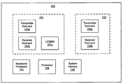
- FIG. 1 is a block diagram of an exemplary system for wireless communication using a plurality of communication protocols, which may be utilized in accordance with an embodiment of the invention.
- a mobile terminal 150 comprising a plurality of transceivers 151 and 152 , a baseband processor 154 , a processor 156 , and system memory 158 .
- the transceivers 151 and 152 may each comprise a transmitter front end 151 a , 152 a , respectively, and a receiver front end 151 b , 152 b , respectively.
- Transceiver 151 may additional comprise a Local Oscillator Generator (LOGEN) 151 c.
- LOGEN Local Oscillator Generator
- the transmitter front ends 151 a and 152 a may comprise suitable logic, circuitry, and/or code that may be adapted to process and transmit RF signals.
- the antennas that may be used to transmit the signals are not shown.
- the transmitter front ends 151 a and 152 a may be communicated baseband signals to be transmitted from a baseband processor, such as, for example, the baseband processor 154 .
- the signals may then be, for example, filtered, amplified, unconverted, and/or modulated for transmission.
- the baseband signal may be analog or digital depending on the functionality of the transmitter front end 151 a or 152 a and the baseband processor 154 .
- the receiver front ends 151 b and 152 b may comprise suitable logic, circuitry, and/or code that may be adapted to receive and process RF signals.
- the antennas that may be used to receive the signals are not shown.
- the receiver front ends 151 b and 152 b may amplify, filter, downconvert, and/or demodulate the received signals to generate a baseband signal.
- the baseband signal may be analog or digital depending on the functionality of the receiver front end 151 b or 152 b and the baseband processor 154
- the LOGEN 151 c may comprise suitable logic, circuitry, and/or code that may enable generating clock signals that may be utilized in RF transmission and/or reception.
- the baseband processor 154 may comprise suitable logic, circuitry, and/or code that may be adapted to process received baseband signals from the receiver front ends 151 b and 152 b .
- the baseband processor 154 also may comprise suitable logic, circuitry, and/or code that may be adapted to process a baseband signal for communication to the transmitter front ends 151 a and 152 a .
- the baseband processor 154 may be depicted as a single block, the invention need not be so limited. Accordingly, other embodiments of the invention may comprise a plurality of baseband processors for processing signals to and/or from the transceivers 151 and 152 .
- the baseband processor 154 may be utilized to generate control words that may be utilized to control the DDFS.
- the baseband processor 154 may also be utilized to determine the scale factors for signal dividers that may be utilized in clock signal derivations. These derived clock signals may be utilized to clock FM transmit, FM receive, and/or Bluetooth transmit and Bluetooth receive functions.
- the processor 156 may comprise suitable logic, circuitry, and/or code that may be adapted to control the operations of the transceivers 151 and 152 and/or the baseband processor 154 .
- the processor 156 may be utilized to update and/or modify programmable parameters and/or values in a plurality of components, devices, and/or processing elements in the transceivers 151 and 152 and/or the baseband processor 154 .
- Control and/or data information may also be transferred to and/or from another controller and/or processor in the mobile terminal 150 to the processor 156 .
- the processor 156 may transfer control and/or data information to another controller and/or processor in the mobile terminal 150 .
- the processor 156 may utilize the received control and/or data information to determine a mode of operation for the transceivers 151 and/or 152 . For example, the processor 156 may control each of the receiver front ends 151 b and 152 b to receive RF signals at a specific frequency. Similarly, the processor 156 may control each of the transmitter front ends 151 a and 152 a to transmit RF signals at a specific frequency. The processor 156 may also adjust a specific gain for a variable gain amplifier, and/or adjust filtering characteristics for a filter.
- a specific frequency selected and/or parameters needed to calculate the specific frequency, and/or the specific gain value and/or the parameters needed to calculate the specific gain may be stored in the system memory 158 via the controller/processor 156 .
- This information stored in system memory 158 may be transferred to the receiver front end 152 from the system memory 158 via the controller/processor 156 .
- the system memory 158 may comprise suitable logic, circuitry, and/or code that may be adapted to store a plurality of control and/or data information, including parameters needed to calculate frequencies and/or gain, and/or the frequency value and/or gain value.
- the processor 156 may be utilized to generate control words that may be utilized to control the DDFS.
- the mobile terminal 150 may enable two simultaneous RF communications.
- the plurality of transceivers, 151 and 152 may enable performing RF transmission and/or reception operations pertaining to different interfaces at the same time.
- the mobile terminal 150 may be utilized to support simultaneous Bluetooth® and FM.
- the transceiver 151 may be utilized to support Bluetooth® communication
- the transceiver 152 may be utilized to support the FM transmit and receive functions.
- the processor 156 , baseband processor 154 , and system memory 158 may be utilized to control and support the two simultaneous RF communications, for example Bluetooth® and FM, by providing necessary control and data the may enable the plurality of the transceivers, 151 and 152 , to perform RF transmission and/or reception.
- the LOGEN 151 c may be utilized for generating clock signaling necessary for RF transmission and/or reception, for example Bluetooth®, in transceiver 151 . Furthermore, the LOGEN 151 c may also be utilized to simultaneously generate clock signaling for a second RF transmission and/or reception, for example FM, in transceiver 152 .
- the processor 156 , baseband processor 154 , and system memory 158 may be utilized to control and support such clock signaling operations.
- the processor 156 and/or baseband processor 154 may be utilized to control direct digital frequency synthesizers that may be utilized in clock signal generation and derivation operations; also, the processor 156 and/or baseband processor 154 may be utilized to provide any necessary scale factors for signal dividers that may be utilized in clock signal derivations.
- FIG. 2A is a block diagram of an exemplary system for wireless communication using a single BT LOGEN to clock the BT and FM transceivers, which may be utilized in accordance with an embodiment of the invention.
- a wireless terminal 200 comprising a BT transceiver 202 , a BT LOGEN 204 , a divider block 206 a , a divider block 206 b , a DDFS 208 , a DDFS 214 , an FM receiver 210 , a frequency word control block 212 a , a frequency word control block 212 b , and an FM transmitter 216 .
- the BT transceiver 202 may comprise suitable logic, circuitry, and/or code that may enable reception and transmission of Bluetooth® signals.
- the BT transceiver 202 may be similar, for example, to the transceiver 151 and/or 153 . Accordingly, the BT transceiver 202 may transmit and receive RF signals at frequencies used for Bluetooth® communication.
- the BT LOGEN 204 may comprise suitable logic and/or circuitry that may enable generation of a desired local oscillator (LO) signal for use by, for example, a transceiver, such as the BT transceiver 202 .
- the BT LOGEN 204 may generate a plurality of LO signals with the same frequency, but different phases. For example, the BT LOGEN 204 may generate (I) and (Q) signals for use by the Bluetooth® transceiver 202 .
- General operation of a PLL is described in more detail with respect to FIG. 2B and FIG. 2C .
- the FM receiver 210 may comprise suitable logic, circuitry, and/or code that may enable reception of RF signals at FM radio spectrum.
- the FM transmitter 216 may comprise suitable logic, circuitry, and/or code that may enable transmission of RF signals at FM radio spectrum.
- the divider block 206 a may comprise suitable logic, circuitry, and/or code that may enable reducing a frequency of an input signal to an output signal with a desired frequency.
- the output signal generated by the divider block 206 a may be used, for example, as a reference clock for the DDFS 208 .
- the divider block 206 b may comprise similar to divider bock 206 a .
- the output signal generated by the divider block 206 b may be used, for example, as a reference clock for the DDFS 214 .
- the DDFS 208 may generate at least one output signal that may be used as a LO signal for transmission and reception of RF signals by the FM transmitter 210 .
- the DDFS 208 may be utilized to generate, for example, (I) and (Q) LO signals for use by the FM receiver 210 .
- the frequency word control block 212 a may comprise suitable logic, circuitry, and/or code that may enable generation of frequency word controls for the DDFS 208 .
- the frequency word controls may be used by the DDFS 208 to determine the frequency and/or phase of the output signals of the DDFS 208 .
- the frequency word control block 212 a may vary the frequency word controls to the DDFS 208 depending on the frequency of the input signal and the desired output frequency.
- the DDFS 214 and frequency word control block 212 b may be comprised similar to the DDFS 208 and frequency word control block 212 a , and operate in similar manner in conjunction with the FM transmitter 216 .
- the BT LOGEN 204 may be utilized to generate appropriate LO signals that may be used for the Bluetooth® transceiver 202 .
- the LO signals generated by the BT LOGEN 204 may be used for frequency hopping by the Bluetooth® transceiver 202 . Accordingly, frequencies of the (I) and O signals may vary.
- the signal from the BT LOGEN 204 may be divided by the divider blocks 206 a and 206 b using appropriate scale factors, for example N FM — Rx and N FM — Tx , such that it may be an appropriate reference clock signal for the DDFS 208 and the DDFS 214 .
- the scale factors may be determined by, for example, a processor such as the baseband processor 154 and/or the processor 156 .
- the signal from the divider block 206 a may be communicated to the DDFS 208 as a reference clock. Since the input to the divider block 206 a may change as the BT transceiver 202 engages in frequency hopping, the output of the divider block 206 a may also change frequencies. Accordingly, the frequency word control block 212 a may vary the frequency word control to compensate for the changing input reference clock. Similarly, the frequency word control block 212 b may vary the frequency word control to compensate for the changing input reference clock inputted into the DDFS 214 from the divider block 206 b as a result of variations caused by Bluetooth® hopping. Other embodiments of the invention may also control the divider blocks 206 a and 206 b to change the frequency of its output signal.
- the DDFS 208 and the DDFS 214 may output a desired frequency by controlling the frequency of the input reference clock signal and the value of the frequency word control.
- the digital signals generated by the frequency word control block 212 a and the frequency word control block 212 b may comprise control information about the frequency and/or phase of the analog output signal that may be generated by the DDFS 208 and 214 .
- the processor 156 and/or processor 154 may also be utilized to control the DDFSs 208 , 214 , so as to provide necessary data that may enable the DDFSs 208 and/or 214 to perform necessary frequency synthesis, and scale factors utilized by divider 206 a and/or 206 b.
- the BT LOGEN 204 may output (I) and (Q) signals for the BT transceiver 204 .
- the outputs of the DDFS 208 and 214 may comprise (I) and (Q) signals for the FM receiver 210 and the FM transmitter 216 , respectively.
- the input to the divider block 206 a and 206 b may be, for example, one of the (I) and (Q) signals.
- the DDFS 208 may generate (I) and (Q) signals for the FM receiver 210
- the DDFS 214 may generate (I) and (Q) signals for the FM transmitter 216 .
- divider block 206 a and the divider block 206 b may be shown in an embodiment of the invention disclosed with respect to FIG. 2 , the invention need not be so limited.
- a signal that has the same frequency as the output of the BT LOGEN 204 may be used as a reference clock for the DDFS 208 and the DDFS 214 .
- FIG. 2B is a block diagram of an exemplary system for wireless communication using a integrated BT LOGEN to clock the BT and clock FM transceiver at 1.6 GHz, which may be utilized in accordance with an embodiment of the invention.
- BT transceiver 202 there is shown BT transceiver 202 , the BT LOGEN 204 , the divider block 206 a , the divider block 206 b , the DDFS 208 , the DDFS 214 , the FM receiver 210 , the frequency word control block 212 a , the frequency word control block 212 b , the FM transmitter 216 , a digital to analog converter (DAC) 242 a , a digital to analog converter (DAC) 242 b , a filter 244 a , and a filter 244 b .
- DAC digital to analog converter
- DAC digital to analog converter
- the BT transceiver 202 may comprise a Bluetooth (BT) receiver 238 and a Bluetooth (BT) transmitter 240 .
- the BT LOGEN 204 may comprise a voltage controlled oscillator (VCO) 220 , a fractional synthesizer 222 , a plurality of loop amplifiers 224 , 226 , 228 , and 230 , a plurality of mixers 232 and 234 , and a divider 232 .
- VCO voltage controlled oscillator
- the BT LOGEN 204 may comprise suitable logic, circuitry, and/or code that may be enabled to generate a quadrature clock signal f BT comprising an in-phase (I) component f BT — I and a quadrature-phase (Q) component f BT — Q .
- the (I) and (Q) component signals may be communicated to the BT receiver 238 and the BT transmitter 240 .
- the frequency of the generated quadrature clock signal f BT to the BT receiver 238 and the BT transmitter 240 may be about 2.4 GHz, for example, and may be enabled to clock one or more of the BT receiver 238 and the BT transmitter 240 .
- the BT LOGEN 204 may also be utilized to generate an (I) and (Q) component output signals for FM transmission and reception frequencies f FM — Tx and f FM — Rx .
- the frequency of the generated quadrature clock signals f FM — Rx and f FM — Tx to the FM receiver 232 and the FM transmitter 230 may be in the range of 78-100 MHz, for example, and may be enabled to clock one or more of the FM receiver 232 and the FM transmitter 230 .
- the VCO 220 may comprise suitable logic, circuitry, and/or code that may be enabled to generate a clock signal f LO at a particular frequency that may be N times the frequency of the reference oscillator, Nf 0 , for example, where f 0 is the frequency of the reference oscillator.
- the VCO 220 may be enabled to generate a 1.6 GHz clock signal.
- the loop amplifier 216 may comprise suitable logic, circuitry, and/or code that may be enabled to amplify the generated clock signal f LO received from the VCO 220 .
- the loop amplifier 224 may comprise suitable logic, circuitry, and/or code that may be enabled to generate an amplified output signal to the plurality of mixers 234 and 236 , and the divider 232 .
- the loop amplifier 226 may comprise suitable logic, circuitry, and/or code that may be enabled to amplify a received signal from the loop amplifier 224 and generate an amplified output signal to the fractional synthesizer 222 .
- the fractional synthesizer 222 may comprise suitable logic, circuitry, and/or code that may be enabled to divide the output of the VCO 220 by N, for example, to match the frequency of a reference oscillator.
- the fractional synthesizer 222 may be programmable to synthesize a plurality of closely spaced frequencies, which enables it to be utilized in commercial wireless applications with multiple channels.
- the fractional synthesizer 222 may be enabled to adjust a clock signal f LO generated by the VCO 220 without affecting the quadrature clock signals f BT communicated to the Bluetooth transceiver 204 .
- the divider 232 may comprise suitable logic, circuitry, and/or code that may be enabled to divide a frequency of a received input signal into one or more signals with different frequencies.
- the divider 232 may be enabled to receive a 1.6 GHz input signal from the loop amplifier 224 and generate two 800 MHz output signals, for example, to the plurality of mixers 234 and 236 .
- the divider 232 may be enabled to generate an output clock signal f DIV by dividing a frequency of the generated clock signal f LO .
- the mixer 234 may comprise suitable logic, circuitry, and/or code that may be enabled to mix the received input signals from the loop amplifier 224 and the divider 232 and generate an output signal to the loop amplifier 228 .
- the mixer 234 may be enabled to mix a 1.6 GHz input signal from the loop amplifier 224 and a 800 MHz input signal from the divider 232 and generate a 2.4 GHz output signal to the loop amplifier 228 .
- the loop amplifier 228 may be enabled to amplify the received input signal from the mixer 234 and generate an amplified output signal to one or more of the BT receiver 238 and the BT transmitter 240 .
- the loop amplifier 228 may be enabled to generate the (Q) component f BT — Q of the amplified output signal to one or more of the BT receiver 238 and the BT transmitter 240 .
- the mixer 236 may comprise suitable logic, circuitry, and/or code that may be enabled to mix the received input signals from the loop amplifier 224 and the divider 232 and generate an output signal to the loop amplifier 230 .
- the mixer 236 may be enabled to mix a 1.6 GHz input signal from the loop amplifier 224 and a 800 MHz input signal from the divider 232 and generate a 2.4 GHz output signal to the loop amplifier 230 .
- the loop amplifier 230 may be enabled to amplify the received input signal from the mixer 236 and generate an amplified output signal to one or more of the BT receiver 238 and the BT transmitter 240 .
- the loop amplifier 230 may be enabled to generate the (I) component f BT — I of the amplified output signal to one or more of the BT receiver 238 and the BT transmitter 240 .
- the fractional synthesizer 222 may be enabled to generate a control signal, which may be utilized by the VCO 220 to generate a clock signal f LO .
- the frequency of the clock signal, f LO may be about 1.6 GHz.
- the fractional synthesizer 222 may utilize the clock signal, f LO to adjust a subsequent control signal communicated to the VCO 220 .
- the clock signal, f LO may be communicated to a divider 232 , which may implement frequency division on the received signal f LO .
- the divider 232 may generate an output clock signal, f DIV comprising in-phase (I) component frequency division signal, f DIV — I , and a quadrature-phase (Q) component frequency division signal, f DIV — Q .
- f DIV in-phase (I) component frequency division signal
- Q quadrature-phase
- the mixer 236 may be enabled to mix the signals, f LO and f DIV — I , and generate a signal f BT — I .
- the mixer 234 may mix the signals, f LO and f DIV — Q , and generate a signal f BT — Q .
- the signals f BT — I and f BT — Q may be communicated to the BT receiver 238 and/or to the BT transmitter 240 .
- the frequency of the signals f BT — I and f BT — Q may be about 2.4 GHz.
- the clock signal f LO may be communicated to the divider blocks 206 a and 206 b , where clock signal may be reduced by a control factor as described above.
- the clock signal f LO may also be communicated directly to the DDFS 208 and 214 .
- the DDFS 208 and 214 may be enabled to receive a clock signal, which may either be the clock signal f LO or the output signals from the divider blocks 206 a and 206 b respectively, and generate a sequence of binary numbers.
- the process of converting the DDFS input signal to a sequence of binary numbers may comprise analog to digital conversion (ADC) whereby each distinct voltage, current and/or power level associated with the received clock signal may be represented as a binary number selected from a plurality of binary numbers. Conversely, each binary number may correspond to a range of voltage, current and/or power levels in the received clock signal.
- An exemplary clock signal, f LO may be a sinusoidal signal for which the corresponding period may be equal to the inverse of the frequency, (1/f LO ).
- the number of binary numbers in the plurality may be determined by the number of bits, b, in the binary number representation. Each binary number may comprise a least significant bit (LSB) and a most significant bit (MSB).
- each of binary numbers may have a value within the range 0 to 2 b ⁇ 1.
- the operation of the DDFS 208 may be such that a period of the received clock signal, f LO may be converted to a binary sequence 0, 1, . . . , 2 b ⁇ 1, wherein upon reaching the value 2 b ⁇ 1 the next number in the binary sequence may be 0 with the sequence continuing.
- the set of numbers from 0 to 2 b ⁇ 1 may represent a period of the binary sequence.
- the DDFS 208 may receive a frequency word control input signal, f Word — Rx , from the processor 212 a upon which the value of b may be determined.
- the period of the sequence of binary numbers generated by the DDFS may be programmable based on the f Word — Rx input signal.
- the DDFS 214 may operate in similar manner wherein the processor 212 b may communicate another frequency word control input signal f Word — Tx that is specifically configured to desired frequency from FM transmission.
- the DAC 242 a and 242 b may comprise suitable logic, circuitry and/or code that may enable generation of an analog output signal based on a received sequence of input binary numbers.
- the DAC 242 a and 242 b may be enabled to generate corresponding analog voltage levels for each input binary number.
- the number of distinct analog voltage levels may be equal to the number of distinct binary numbers in the input sequence.
- the filter 244 a may comprise suitable logic, circuitry and/or code that may enable low pass filtering (LPF) of signal components contained in a received input signal.
- the filter 244 a may enable smoothing of the received input signal to attenuate amplitudes for undesirable frequency components contained in the received input signal.
- the filter 244 a may generate a signal, f FM — Rx , having a frequency in the FM frequency band.
- the range of frequencies for the signal f FM — Rx may be between about 78 MHz and 100 MHz, for example.
- the signal f FM — Rx may be a quadrature signal comprising (I) and (Q) signal components.
- the 78-100 MHz (I) and (Q) signals may be communicated to an FM receiver 210 .
- the filter 244 b may be similar to 244 a , and may be utilized in similar manner to generate a signal f FM — Tx , having a frequency in the FM frequency band.
- the range of frequencies for the signal f FM — Tx may be between about 78 MHz and 100 MHz, for example.
- the signal f FM — Tx may be a quadrature signal comprising (I) and (Q) signal components.
- the 78-100 MHz (I) and (Q) signals may be communicated to an FM transmitter 210 .
- the FM frequencies f FM — Rx and f FM — Tx may be different.
- the value f Word — Tx and f Word — Rx may be selected to maintain an approximately constant frequency for the signals f FM — Rx and f FM — Tx despite changes that may occur in the signal f LO , which may occur due to frequency hopping in the Bluetooth communication signal.
- FIG. 2C is a block diagram of an exemplary system for wireless communication using a integrated BT LOGEN to clock the BT and clock FM transceiver at 800 MHz, which may be utilized in accordance with an embodiment of the invention.
- the BT transceiver 202 there is shown the BT transceiver 202 , the BT LOGEN 204 , the divider block 206 a , the divider block 206 b , the DDFS 208 , the DDFS 214 , the FM receiver 210 , the frequency word control block 212 a , the frequency word control block 212 b , the FM transmitter 216 , the digital to analog converter (DAC) 242 a , the digital to analog converter (DAC) 242 b , the filter 244 a , and a filter 244 b .
- DAC digital to analog converter
- DAC digital to analog converter
- the BT transceiver 202 may comprise the Bluetooth (BT) receiver 238 and the Bluetooth (BT) transmitter 240 .
- the BT LOGEN 204 may comprise the voltage controlled oscillator (VCO) 220 , the fractional synthesizer 222 , the plurality of loop amplifiers 224 , 226 , 228 , and 230 , the plurality of mixers 232 and 234 , and the divider 232 .
- VCO voltage controlled oscillator
- the components may be substantially similar to the corresponding components described with respect to FIG. 2B .
- the signal f DIV — I or the signal f DIV — Q may be utilized instead.
- the clock signal f DIV — Q may be communicated to the divider blocks 206 a and 206 b .
- the clock signal f DIV — Q may also be communicated directly to the DDFS 208 and 214 .
- the DDFS 208 and 214 may be enabled to receive a clock signal, which may either be the clock signal f DIV — I the output signals from the divider blocks 206 a and 206 b respectively, and generate a sequence of binary numbers.
- the process of converting the DDFS input signal to a sequence of binary numbers may comprise analog to digital conversion (ADC) whereby each distinct voltage, current and/or power level associated with the received clock signal may be represented as a binary number selected from a plurality of binary numbers. Conversely, each binary number may correspond to a range of voltage, current and/or power levels in the received clock signal.
- An exemplary clock signal, f LO may be a sinusoidal signal for which the corresponding period may be equal to the inverse of the frequency, (1/f DIV — Q ).
- the number of binary numbers in the plurality may be determined by the number of bits, b, in the binary number representation. Each binary number may comprise a least significant bit (LSB) and a most significant bit (MSB).
- each of binary numbers may have a value within the range 0 to 2 b ⁇ 1.
- the operation of the DDFS 208 may be such that a period of the received clock signal, f LO may be converted to a binary sequence 0, 1, . . . , 2 b ⁇ 1, wherein upon reaching the value 2 b ⁇ 1 the next number in the binary sequence may be 0 with the sequence continuing.
- the set of numbers from 0 to 2 b ⁇ 1 may represent a period of the binary sequence.
- the DDFS 208 may receive a frequency word input signal, f Word — Rx , from the processor 212 a upon which the value of b may be determined.
- the period of the sequence of binary numbers generated by the DDFS may be programmable based on the f Word — Rx input signal.
- the DDFS 214 may operate in similar manner wherein the processor 212 b may communicate another f Word — Tx that is specifically configured to desired frequency from FM transmission.
- the DAC 242 a and 242 b may comprise suitable logic, circuitry and/or code that may enable generation of an analog output signal based on a received sequence of input binary numbers.
- the DAC 242 a and 242 b may be enabled to generate corresponding analog voltage levels for each input binary number.
- the number of distinct analog voltage levels may be equal to the number of distinct binary numbers in the input sequence.
- the filter 244 a may comprise suitable logic, circuitry and/or code that may enable low pass filtering (LPF) of signal components contained in a received input signal.
- the filter 244 a may enable smoothing of the received input signal to attenuate amplitudes for undesirable frequency components contained in the received input signal.
- the filter 244 a may generate a signal, f FM — Rx , having a frequency in the FM frequency band.
- the range of frequencies for the signal f FM — Rx may be between about 78 MHz and 100 MHz, for example.
- the signal f FM — Rx may be a quadrature signal comprising (I) and (Q) signal components.
- the 78-100 MHz (I) and (Q) signals may be communicated to an FM receiver 210 .
- the filter 244 b may be similar to 244 a , and may be utilized in similar manner to generate a signal f FM — Tx , having a frequency in the FM frequency band.
- the range of frequencies for the signal f FM — Tx may be between about 78 MHz and 100 MHz, for example.
- the signal f FM — Tx may be a quadrature signal comprising (I) and (Q) signal components.
- the 78-100 MHz (I) and (Q) signals may be communicated to an FM transmitter 210 .
- the FM frequencies f FM — Rx and f FM — Tx may be different.
- the value f Word — Tx and f Word — Rx may be selected to maintain an approximately constant frequency for the signals f FM — Rx and f FM — Tx despite changes that may occur in the signal f DIV — Q , which may occur due to frequency hopping in the Bluetooth communication signal. Also, because the clock signal used is f DIV — Q instead of f LO , the values used for f Word — Tx and f Word — Rx in this embodiment may also be different from the values used in the embodiment described in FIG. 2B .
- FIG. 2D is a block diagram of an exemplary system for wireless communication using an integrated BT LOGEN to clock the BT and clock FM transceiver via a MUX with plurality of input frequencies, which may be utilized in accordance with an embodiment of the invention.
- the BT transceiver 202 may comprise the Bluetooth (BT) receiver 238 and the Bluetooth (BT) transmitter 240 .
- the BT LOGEN 204 may comprise the voltage controlled oscillator (VCO) 220 , the fractional synthesizer 222 , the plurality of loop amplifiers 224 , 226 , 228 , and 230 , the plurality of mixers 232 and 234 , and the divider 232 .
- VCO voltage controlled oscillator
- the MUX 246 may comprise suitable logic, circuitry and/or code that may enable outputting a signal which is selected from a plurality of input signals.
- the other components may be substantially similar to the corresponding components described with respect to FIG. 2B and FIG. 2C .
- F LO , F Div — Q and F Div — I may be inputted into the MUX 246 .
- the MUX 246 may then receive Select input , which may be utilized by the MUX 246 to select an input from the plurality of inputs.
- the MUX 246 may output a signal by choosing a single from F LO , F Div — Q and F Div — I based on Select input .
- the output signal from the MUX 246 may be inputted into divider blocks 206 a and 206 b , and subsequently utilized to clock DDFS 208 and DDFS 214 as described with respect to FIG. 2B . and FIG. 2C .
- FIG. 3 is a block diagram illustrating an exemplary direct digital frequency synthesizer, which may be utilized in accordance with an embodiment of the invention.
- a direct digital frequency synthesizer (DDFS) 300 comprising a phase accumulator 302 , a phase-to-sine amplitude converter 304 , and a digital to analog converter (DAC) 306 .
- the DDFS 300 may be similar in functionality to the DDFS 208 and 214 .
- the phase accumulator 302 may comprise an adder 302 a that may enable integrating an input signal, such as, for example, a frequency word control CTRL, by adding it to a previous integrated value stored in a register 302 b on each cycle of a reference clock F ref .
- the reference clock F ref may be fixed-frequency or varying frequency. In the case of a varying reference clock F ref , the change in frequency may be compensated by altering the frequency word control CTRL such that the output of the DDFS may comprise a desired frequency and/or phase.
- the phase-to-sine amplitude converter 304 may comprise suitable logic, circuitry, and/or code that may enable conversion of the output of the phase accumulator 302 to an approximated sine amplitude. For example, the conversion may be achieved via a look-up table. Although only a single output may be shown for exemplary purposes, a plurality of signals may be generated where each signal may be phase shifted from the others. For example, where (I) and (Q) signals may be needed, the phase-to-sine amplitude converter 304 may utilize a plurality of different look-up tables for each input value. In an exemplary embodiment of the invention, a first look-up table may be utilized for the (I) signal and a second look-up table may be utilized for the (Q) signal.
- the DAC 306 may comprise suitable logic and/or circuitry that may enable converting the digital output of the phase-to-sine amplitude converter 304 to an analog output.
- the DAC 306 may also comprise, for example, a low-pass filter that may be used to “smooth” the analog output.
- the DDFS 300 may generate, for example, (I) and (Q) signals, there may be a DAC for generating an (I) signal and a DAC for generating a (Q) signal.
- the DDFS 300 may be a digitally-controlled signal generator that may vary phase, frequency, and/or amplitude of one or more output signals based on a single reference clock F ref and an input control word, CTRL.
- the input control word, CTRL may be provided to the adder 302 a , and may be successively added to an integrated value stored in the register 302 b .
- the adding may occur, for example, on each cycle of the reference clock F ref .
- the sum may eventually be greater than the maximum value the accumulator can store, and the value in the accumulator may overflow or “wrap”.
- the output of the phase accumulator 302 which may be referred to as F out may be periodic at a period of 1/F out and may represent the phase angle of a signal.
- the DDFS 322 may operate as a frequency generator that generates one or more sine waves or other periodic waveforms over a large range of frequencies, from almost DC to approximately half the reference clock frequency F ref .
- the state of the DDFS 300 may be saved in, for example, a memory such as the system memory 158 , described with respect to FIG. 1A .
- the output signal F out may be interrupted and then resumed without losing the phase information comprising the generated signals.
- the DDFS 300 may resume generating the output signal F out using the saved state loaded from, for example, the system memory 158 . Accordingly, the output signal F out may resume from the last phase angle transmitted before the signal was interrupted.
- FIG. 4 is a flow diagram illustrating exemplary steps for using digital frequency synthesizers (DDFS) with a plurality of communication protocols to generate clocking signal for FM transceiver, which may be utilized in accordance with an embodiment of the invention.
- exemplary steps may begin at step 400 .
- the VCO 220 may generate a clock signal f LO at a particular frequency, for example, 1.6 GHz utilizing the fractional synthesizer 222 .
- an output clock signal f DIV may be generated by dividing a frequency of the generated clock signal f LO .
- a first quadrature clock signal f BT may be generated by mixing the generated clock signal f LO with the generated output clock signal f DIV .
- the generated first quadrature clock signal f BT may be utilized to enable the transmission and/or reception of the Bluetooth communication signals by the BT transceiver 202 .
- the generated output clock signal f LO may be communicated to two different DDFS.
- the generated clock signal, f Div may be communicated to the DDFS instead of the f LO signal.
- the clock signal whether it is f LO or f Div , may be communicated first to signal dividers where the signal may be reduced by a scaling factor.
- the two DDFS may enable modification of a frequency of the communicated output clock signal f DIV or communicated clock signal f LO based on received control word frequencies f WORD — Tx and/or f WORD — Rx .
- the control word frequencies may be utilized to compensate for frequency deviations in f LO or f Div , which may be caused by frequency hopping for Bluetooth® communication.
- second quadrature clock signals f FM — Rx and f FM — Tx may be generated utilizing the generated clock signal f LO or the generated output clock signal f DIV to enable the transmission and/or reception of FM communication signals. Control then passes to end step 416 .
- aspects of an exemplary system may comprise, on a chip, the BT LOGEN 204 that may generate an initial signal f LO which may be utilized to clock a Bluetooth® (BT) transceiver 202 .
- the LOGEN may comprise a Voltage Controlled Oscillator (VCO) 220 generating signals in the 1.6 GHz range.
- VCO Voltage Controlled Oscillator
- the generated signal f LO may be utilized to generate a quadrature signal f Div via a signal divider 232 .
- the quadrature signal f Div may comprise an (I) and (Q) phase signals f Div — Q and f Div — I .
- the initial signal f LO may be mixed with the quadrature signal f Div to generate a quadrature Bluetooth (BT) clock frequency f BT , which may comprise (I) and (Q) LO signals f BT — Q and f BT — I .
- BT Bluetooth
- the BT LOGEN 204 may also be utilized to generate clocking signals for FM radio transmission and reception.
- the initial signal f LO may be communicated to DDFS 208 and 214 , either directly or via divider blocks 206 a and 206 b .
- the divider block 206 a may reduce the frequency of the input signal by a factor that may be determined by, for example, the baseband processor 154 and/or the processor 156 for FM transmission and/or reception.
- the divider block 206 b may also reduce the frequency of the input signal by a factor that may be determined by, for example, the baseband processor 154 and/or the processor 156 for FM transmission.
- the output of the divider block 206 a may be communicated to the DDFS 208 as a reference clock.
- the DDFS 208 may further reduce the frequency of the signal from the divider block 206 a to generate, for example, f FM — Rx , having (I) and (Q) LO signals, for the FM receiver 210 . Since the DDFS 208 may generate signals with a single frequency at a given time, the FM receiver 210 may operate in a half-duplex mode.
- the output of the divider block 206 b may be communicated to the DDFS 214 as a reference clock.
- the DDFS 214 may further reduce the frequency of the signal from the divider block 206 b to generate, for example, f FM — Tx , having (I) and (Q) LO signals, for the FM transmitter 216 . Since the DDFS 214 may generate signals with a single frequency at a given time, the FM transmitter 216 may operate in a half-duplex mode. The FM transmit frequency and the FM receive frequency may comprise different frequencies.
- the Digital-Analog-Converters (DAC) 242 a and 242 b may enable conversion of the output signals of DDFS 208 and 214 from analog to digital; the Low Pass Filters (LPF) 244 a and 244 b may be utilized to filter the output signals of the DDFS 208 and 214 before being communicated to the FM receiver 210 and FM transmitter 216 .
- LPF Low Pass Filters
- each DDFS may be a constant frequency while the inputs to each DDFS may vary in frequency.
- the Bluetooth® LO signal may vary in frequency as Bluetooth® frequency hopping occurs, the FM LO signals may remain constant for a specific channel frequency.
- the DDFS may utilize frequency control words inputted from processors.
- Time division duplexing of transmission of FM signals and reception of FM signals may be performed by switching the frequency control words between a plurality of values in successive time intervals.
- Another embodiment of the invention may provide a machine-readable storage, having stored thereon, a computer program having at least one code section executable by a machine, thereby causing the machine to perform the steps as described herein for using the BT LOGEN to clock two or more DDFS that may be utilized to enable FM transmission and FM reception.
- the present invention may be realized in hardware, software, or a combination of hardware and software.
- the present invention may be realized in a centralized fashion in at least one computer system, or in a distributed fashion where different elements are spread across several interconnected computer systems. Any kind of computer system or other apparatus adapted for carrying out the methods described herein is suited.
- a typical combination of hardware and software may be a general-purpose computer system with a computer program that, when being loaded and executed, controls the computer system such that it carries out the methods described herein.
- the present invention may also be embedded in a computer program product, which comprises all the features enabling the implementation of the methods described herein, and which when loaded in a computer system is able to carry out these methods.
- Computer program in the present context means any expression, in any language, code or notation, of a set of instructions intended to cause a system having an information processing capability to perform a particular function either directly or after either or both of the following: a) conversion to another language, code or notation; b) reproduction in a different material form.
Abstract
Description
f BT
and
f BT
The signals fBT
F out=(F ref*CTRL)/2N [2]
Claims (36)
Priority Applications (1)
| Application Number | Priority Date | Filing Date | Title |
|---|---|---|---|
| US11/754,708 US7885683B2 (en) | 2007-03-19 | 2007-05-29 | Method and system for simultaneous FM transmit and FM receive functions using an integrated bluetooth local oscillator generator (LOGEN) |
Applications Claiming Priority (2)
| Application Number | Priority Date | Filing Date | Title |
|---|---|---|---|
| US89569807P | 2007-03-19 | 2007-03-19 | |
| US11/754,708 US7885683B2 (en) | 2007-03-19 | 2007-05-29 | Method and system for simultaneous FM transmit and FM receive functions using an integrated bluetooth local oscillator generator (LOGEN) |
Publications (2)
| Publication Number | Publication Date |
|---|---|
| US20080233873A1 US20080233873A1 (en) | 2008-09-25 |
| US7885683B2 true US7885683B2 (en) | 2011-02-08 |
Family
ID=39774079
Family Applications (32)
| Application Number | Title | Priority Date | Filing Date |
|---|---|---|---|
| US11/750,091 Active 2027-11-22 US7586458B2 (en) | 2007-03-19 | 2007-05-17 | Method and system for using a transformer for FM transmit and FM receive functionality |
| US11/750,103 Active 2027-11-17 US7683851B2 (en) | 2007-03-19 | 2007-05-17 | Method and system for using a single transformer for FM transmit and FM receive functions |
| US11/750,111 Expired - Fee Related US7821472B2 (en) | 2007-03-19 | 2007-05-17 | Method and system for FM transmit and FM receive using a transformer as a duplexer |
| US11/750,095 Active 2028-08-12 US7825871B2 (en) | 2007-03-19 | 2007-05-17 | Method and system for equalizing antenna circuit matching variations |
| US11/752,025 Active 2027-07-10 US7564302B2 (en) | 2007-03-19 | 2007-05-22 | Method and system for gain control and power saving in broadband feedback low-noise amplifiers |
| US11/752,754 Active 2029-09-15 US7933568B2 (en) | 2007-03-19 | 2007-05-23 | Method and system for mitigating receiver saturation during simultaneous FM transmission and reception |
| US11/753,698 Expired - Fee Related US8369889B2 (en) | 2007-03-19 | 2007-05-25 | Method and system for sharing a single antenna for frequency modulation (FM) transmission, FM reception and near field communication (NFC) |
| US11/753,708 Expired - Fee Related US8238825B2 (en) | 2007-03-19 | 2007-05-25 | Method and system for sharing a single antenna for frequency modulation (FM) reception or FM transmission and near field communication (NFC) |
| US11/754,481 Active 2030-08-07 US8175543B2 (en) | 2007-03-19 | 2007-05-29 | Method and system for wireless communication using integrated clock generation for bluetooth and FM transmit and FM receive functions |
| US11/754,600 Active 2029-10-10 US7937107B2 (en) | 2007-03-19 | 2007-05-29 | Method and system for Bluetooth, near field communication and simultaneous FM transmission and reception functions |
| US11/754,467 Active 2031-10-24 US8600315B2 (en) | 2007-03-19 | 2007-05-29 | Method and system for a configurable front end |
| US11/754,499 Abandoned US20080233868A1 (en) | 2007-03-19 | 2007-05-29 | Method and system for sharing a single antenna for frequency modulation (fm) transmit or fm receive, and near field communicaiton (nfc) |
| US11/754,708 Active 2029-09-26 US7885683B2 (en) | 2007-03-19 | 2007-05-29 | Method and system for simultaneous FM transmit and FM receive functions using an integrated bluetooth local oscillator generator (LOGEN) |
| US11/754,438 Expired - Fee Related US7915999B2 (en) | 2007-03-19 | 2007-05-29 | Method and system for simultaneous transmission and reception of FM signals utilizing a DDFS clocked by an RFID PLL |
| US11/754,581 Active 2029-10-02 US7925222B2 (en) | 2007-03-19 | 2007-05-29 | Method and system for simultaneous FM transmission and FM reception using a shared antenna and a direct digital frequency synthesizer |
| US11/754,705 Expired - Fee Related US7995971B2 (en) | 2007-03-19 | 2007-05-29 | Method and system for clocking FM transmit FM receive, and near field communication functions using DDFS |
| US11/754,407 Active 2029-08-28 US7920893B2 (en) | 2007-03-19 | 2007-05-29 | Method and system for transmission or reception of FM signals utilizing a DDFS clocked by an RFID PLL |
| US11/754,472 Active 2027-06-29 US7554404B2 (en) | 2007-03-19 | 2007-05-29 | Method and system for a low noise amplifier with tolerance to large inputs |
| US11/754,460 Abandoned US20080232522A1 (en) | 2007-03-19 | 2007-05-29 | Method and System for Integration of Bluetooth and FM Local Oscillator Generation into a Single Unit Using a DDFS |
| US11/754,490 Expired - Fee Related US8005436B2 (en) | 2007-03-19 | 2007-05-29 | Method and system for integrated bluetooth transceiver, FM transmitter and FM receiver |
| US11/754,768 Active 2030-01-29 US8032175B2 (en) | 2007-03-19 | 2007-05-29 | Method and system for using a bluetooth PLL to drive FM transmit, FM receive, bluetooth, and NFC functions |
| US11/754,621 Abandoned US20080232507A1 (en) | 2007-03-19 | 2007-05-29 | Method and System for Simultaneous FM Transmission and FM Reception Using a Shared Antenna and an Integrated Local Oscillator Generator |
| US11/864,754 Active 2029-06-15 US8509356B2 (en) | 2007-03-19 | 2007-09-28 | Method and system for blocker and/or leakage signal rejection by DC bias cancellation |
| US12/485,547 Abandoned US20090251210A1 (en) | 2007-03-19 | 2009-06-16 | Method And System For Gain Control And Power Saving In Broadband Feedback Low-Noise Amplifiers |
| US12/536,059 Expired - Fee Related US8018393B2 (en) | 2007-03-19 | 2009-08-05 | Method and system for using a transformer for FM transmit and FM receive functionally |
| US12/910,167 Abandoned US20110037677A1 (en) | 2007-03-19 | 2010-10-22 | Method and system for fm transmit and fm receive using a transformer as a duplexer |
| US12/917,799 Expired - Fee Related US7990333B2 (en) | 2007-03-19 | 2010-11-02 | Method and system for equalizing antenna circuit matching variations |
| US13/080,036 Active US8437706B2 (en) | 2007-03-19 | 2011-04-05 | Method and system for transmission or reception of FM signals utilizing a DDFS clocked by an RFID PLL |
| US13/099,457 Active US8249650B2 (en) | 2007-03-19 | 2011-05-03 | Method and system for bluetooth, near field communication and simultaneous FM transmission and reception functions |
| US13/206,240 Active US8145140B2 (en) | 2007-03-19 | 2011-08-09 | Method and system for clocking FM transmit, FM receive, and near field communication functions using DDFS |
| US13/207,556 Abandoned US20110291911A1 (en) | 2007-03-19 | 2011-08-11 | Method and System for Using a Transformer for FM Transmit and FM Receive Functionality |
| US13/558,187 Active 2028-08-27 US9160288B2 (en) | 2007-03-19 | 2012-07-25 | Method and system for sharing a single antenna for frequency modulation (FM) reception or FM transmission and near field communication (NFC) |
Family Applications Before (12)
| Application Number | Title | Priority Date | Filing Date |
|---|---|---|---|
| US11/750,091 Active 2027-11-22 US7586458B2 (en) | 2007-03-19 | 2007-05-17 | Method and system for using a transformer for FM transmit and FM receive functionality |
| US11/750,103 Active 2027-11-17 US7683851B2 (en) | 2007-03-19 | 2007-05-17 | Method and system for using a single transformer for FM transmit and FM receive functions |
| US11/750,111 Expired - Fee Related US7821472B2 (en) | 2007-03-19 | 2007-05-17 | Method and system for FM transmit and FM receive using a transformer as a duplexer |
| US11/750,095 Active 2028-08-12 US7825871B2 (en) | 2007-03-19 | 2007-05-17 | Method and system for equalizing antenna circuit matching variations |
| US11/752,025 Active 2027-07-10 US7564302B2 (en) | 2007-03-19 | 2007-05-22 | Method and system for gain control and power saving in broadband feedback low-noise amplifiers |
| US11/752,754 Active 2029-09-15 US7933568B2 (en) | 2007-03-19 | 2007-05-23 | Method and system for mitigating receiver saturation during simultaneous FM transmission and reception |
| US11/753,698 Expired - Fee Related US8369889B2 (en) | 2007-03-19 | 2007-05-25 | Method and system for sharing a single antenna for frequency modulation (FM) transmission, FM reception and near field communication (NFC) |
| US11/753,708 Expired - Fee Related US8238825B2 (en) | 2007-03-19 | 2007-05-25 | Method and system for sharing a single antenna for frequency modulation (FM) reception or FM transmission and near field communication (NFC) |
| US11/754,481 Active 2030-08-07 US8175543B2 (en) | 2007-03-19 | 2007-05-29 | Method and system for wireless communication using integrated clock generation for bluetooth and FM transmit and FM receive functions |
| US11/754,600 Active 2029-10-10 US7937107B2 (en) | 2007-03-19 | 2007-05-29 | Method and system for Bluetooth, near field communication and simultaneous FM transmission and reception functions |
| US11/754,467 Active 2031-10-24 US8600315B2 (en) | 2007-03-19 | 2007-05-29 | Method and system for a configurable front end |
| US11/754,499 Abandoned US20080233868A1 (en) | 2007-03-19 | 2007-05-29 | Method and system for sharing a single antenna for frequency modulation (fm) transmit or fm receive, and near field communicaiton (nfc) |
Family Applications After (19)
| Application Number | Title | Priority Date | Filing Date |
|---|---|---|---|
| US11/754,438 Expired - Fee Related US7915999B2 (en) | 2007-03-19 | 2007-05-29 | Method and system for simultaneous transmission and reception of FM signals utilizing a DDFS clocked by an RFID PLL |
| US11/754,581 Active 2029-10-02 US7925222B2 (en) | 2007-03-19 | 2007-05-29 | Method and system for simultaneous FM transmission and FM reception using a shared antenna and a direct digital frequency synthesizer |
| US11/754,705 Expired - Fee Related US7995971B2 (en) | 2007-03-19 | 2007-05-29 | Method and system for clocking FM transmit FM receive, and near field communication functions using DDFS |
| US11/754,407 Active 2029-08-28 US7920893B2 (en) | 2007-03-19 | 2007-05-29 | Method and system for transmission or reception of FM signals utilizing a DDFS clocked by an RFID PLL |
| US11/754,472 Active 2027-06-29 US7554404B2 (en) | 2007-03-19 | 2007-05-29 | Method and system for a low noise amplifier with tolerance to large inputs |
| US11/754,460 Abandoned US20080232522A1 (en) | 2007-03-19 | 2007-05-29 | Method and System for Integration of Bluetooth and FM Local Oscillator Generation into a Single Unit Using a DDFS |
| US11/754,490 Expired - Fee Related US8005436B2 (en) | 2007-03-19 | 2007-05-29 | Method and system for integrated bluetooth transceiver, FM transmitter and FM receiver |
| US11/754,768 Active 2030-01-29 US8032175B2 (en) | 2007-03-19 | 2007-05-29 | Method and system for using a bluetooth PLL to drive FM transmit, FM receive, bluetooth, and NFC functions |
| US11/754,621 Abandoned US20080232507A1 (en) | 2007-03-19 | 2007-05-29 | Method and System for Simultaneous FM Transmission and FM Reception Using a Shared Antenna and an Integrated Local Oscillator Generator |
| US11/864,754 Active 2029-06-15 US8509356B2 (en) | 2007-03-19 | 2007-09-28 | Method and system for blocker and/or leakage signal rejection by DC bias cancellation |
| US12/485,547 Abandoned US20090251210A1 (en) | 2007-03-19 | 2009-06-16 | Method And System For Gain Control And Power Saving In Broadband Feedback Low-Noise Amplifiers |
| US12/536,059 Expired - Fee Related US8018393B2 (en) | 2007-03-19 | 2009-08-05 | Method and system for using a transformer for FM transmit and FM receive functionally |
| US12/910,167 Abandoned US20110037677A1 (en) | 2007-03-19 | 2010-10-22 | Method and system for fm transmit and fm receive using a transformer as a duplexer |
| US12/917,799 Expired - Fee Related US7990333B2 (en) | 2007-03-19 | 2010-11-02 | Method and system for equalizing antenna circuit matching variations |
| US13/080,036 Active US8437706B2 (en) | 2007-03-19 | 2011-04-05 | Method and system for transmission or reception of FM signals utilizing a DDFS clocked by an RFID PLL |
| US13/099,457 Active US8249650B2 (en) | 2007-03-19 | 2011-05-03 | Method and system for bluetooth, near field communication and simultaneous FM transmission and reception functions |
| US13/206,240 Active US8145140B2 (en) | 2007-03-19 | 2011-08-09 | Method and system for clocking FM transmit, FM receive, and near field communication functions using DDFS |
| US13/207,556 Abandoned US20110291911A1 (en) | 2007-03-19 | 2011-08-11 | Method and System for Using a Transformer for FM Transmit and FM Receive Functionality |
| US13/558,187 Active 2028-08-27 US9160288B2 (en) | 2007-03-19 | 2012-07-25 | Method and system for sharing a single antenna for frequency modulation (FM) reception or FM transmission and near field communication (NFC) |
Country Status (1)
| Country | Link |
|---|---|
| US (32) | US7586458B2 (en) |
Cited By (3)
| Publication number | Priority date | Publication date | Assignee | Title |
|---|---|---|---|---|
| US20140084970A1 (en) * | 2006-05-11 | 2014-03-27 | Broadcom Corporation | Low-power ethernet transmitter |
| US8699985B1 (en) * | 2010-04-29 | 2014-04-15 | Agilent Technologies, Inc. | Frequency generator including direct digital synthesizer and signal processor including the same |
| US9729119B1 (en) * | 2016-03-04 | 2017-08-08 | Atmel Corporation | Automatic gain control for received signal strength indication |
Families Citing this family (144)
| Publication number | Priority date | Publication date | Assignee | Title |
|---|---|---|---|---|
| US6765964B1 (en) | 2000-12-06 | 2004-07-20 | Realnetworks, Inc. | System and method for intracoding video data |
| US7065658B1 (en) | 2001-05-18 | 2006-06-20 | Palm, Incorporated | Method and apparatus for synchronizing and recharging a connector-less portable computer system |
| US9026070B2 (en) | 2003-12-18 | 2015-05-05 | Qualcomm Incorporated | Low-power wireless diversity receiver with multiple receive paths |
| US9450665B2 (en) | 2005-10-19 | 2016-09-20 | Qualcomm Incorporated | Diversity receiver for wireless communication |
| US7825745B1 (en) * | 2006-09-12 | 2010-11-02 | Rf Magic Inc. | Variable bandwidth tunable silicon duplexer |
| US20080081631A1 (en) * | 2006-09-29 | 2008-04-03 | Ahmadreza Rofougaran | Method And System For Integrating An NFC Antenna And A BT/WLAN Antenna |
| WO2008089841A1 (en) * | 2007-01-22 | 2008-07-31 | Freescale Semiconductor, Inc. | Calibration signal generator |
| US7978782B2 (en) * | 2007-02-28 | 2011-07-12 | Broadcom Corporation | Method and system for polar modulation using a direct digital frequency synthesizer |
| US8036308B2 (en) * | 2007-02-28 | 2011-10-11 | Broadcom Corporation | Method and system for a wideband polar transmitter |
| US7586458B2 (en) * | 2007-03-19 | 2009-09-08 | Ahmadreza Rofougaran | Method and system for using a transformer for FM transmit and FM receive functionality |
| GB2451435B (en) * | 2007-07-27 | 2012-06-20 | Hewlett Packard Development Co | A Method of enabling the downloading of content |
| US8284704B2 (en) * | 2007-09-28 | 2012-10-09 | Broadcom Corporation | Method and system for utilizing undersampling for crystal leakage cancellation |
| US20090085678A1 (en) * | 2007-09-28 | 2009-04-02 | Ahmadreza Rofougaran | Method and system for signal generation via a digitally controlled oscillator |
| US8116796B2 (en) * | 2008-01-09 | 2012-02-14 | Harris Corporation | Multi-transceiver portable radio communications device and related method |
| US7865138B2 (en) * | 2008-03-28 | 2011-01-04 | Broadcom Corporation | Method and system for a low-complexity multi-beam repeater |
| US9048884B2 (en) * | 2008-05-02 | 2015-06-02 | Lockheed Martin Corporation | Magnetic based short range communications device, system and method |
| US8712334B2 (en) * | 2008-05-20 | 2014-04-29 | Micron Technology, Inc. | RFID device using single antenna for multiple resonant frequency ranges |
| US20110134964A1 (en) * | 2008-08-21 | 2011-06-09 | Nxp B.V. | Frequency synthesizer and configuration for an enhanced frequency-hopping rate |
| USD640976S1 (en) | 2008-08-28 | 2011-07-05 | Hewlett-Packard Development Company, L.P. | Support structure and/or cradle for a mobile computing device |
| US8712324B2 (en) | 2008-09-26 | 2014-04-29 | Qualcomm Incorporated | Inductive signal transfer system for computing devices |
| US8234509B2 (en) * | 2008-09-26 | 2012-07-31 | Hewlett-Packard Development Company, L.P. | Portable power supply device for mobile computing devices |
| US8385822B2 (en) | 2008-09-26 | 2013-02-26 | Hewlett-Packard Development Company, L.P. | Orientation and presence detection for use in configuring operations of computing devices in docked environments |
| US8868939B2 (en) | 2008-09-26 | 2014-10-21 | Qualcomm Incorporated | Portable power supply device with outlet connector |
| US8850045B2 (en) | 2008-09-26 | 2014-09-30 | Qualcomm Incorporated | System and method for linking and sharing resources amongst devices |
| US8401469B2 (en) * | 2008-09-26 | 2013-03-19 | Hewlett-Packard Development Company, L.P. | Shield for use with a computing device that receives an inductive signal transmission |
| US8688037B2 (en) | 2008-09-26 | 2014-04-01 | Hewlett-Packard Development Company, L.P. | Magnetic latching mechanism for use in mating a mobile computing device to an accessory device |
| US8527688B2 (en) | 2008-09-26 | 2013-09-03 | Palm, Inc. | Extending device functionality amongst inductively linked devices |
| DE102008051684B4 (en) * | 2008-10-15 | 2015-06-18 | Airbus Defence and Space GmbH | Transmission / reception means |
| KR101435492B1 (en) * | 2008-10-30 | 2014-08-28 | 삼성전자주식회사 | Antenna deviece for portable wireless terminal |
| US9083686B2 (en) * | 2008-11-12 | 2015-07-14 | Qualcomm Incorporated | Protocol for program during startup sequence |
| EP2377296B1 (en) | 2009-01-05 | 2019-10-16 | QUALCOMM Incorporated | Interior connector scheme for accessorizing a mobile computing device with a removeable housing segment |
| US9509436B2 (en) * | 2009-01-29 | 2016-11-29 | Cubic Corporation | Protection of near-field communication exchanges |
| US8125933B2 (en) * | 2009-02-27 | 2012-02-28 | Research In Motion Limited | Mobile wireless communications device including a differential output LNA connected to multiple receive signal chains |
| US8279018B1 (en) * | 2009-03-16 | 2012-10-02 | Marvell International Ltd. | Trifila balun for wireless transceiver |
| US8232857B1 (en) * | 2009-04-15 | 2012-07-31 | Triquint Semiconductor, Inc. | Flux-coupled transformer for power amplifier output matching |
| US8344959B2 (en) * | 2009-04-30 | 2013-01-01 | Nokia Corporation | Multiprotocol antenna for wireless systems |
| US20100279734A1 (en) * | 2009-04-30 | 2010-11-04 | Nokia Corporation | Multiprotocol Antenna For Wireless Systems |
| US9654792B2 (en) | 2009-07-03 | 2017-05-16 | Intel Corporation | Methods and systems for motion vector derivation at a video decoder |
| US8462852B2 (en) | 2009-10-20 | 2013-06-11 | Intel Corporation | Methods and apparatus for adaptively choosing a search range for motion estimation |
| US8917769B2 (en) * | 2009-07-03 | 2014-12-23 | Intel Corporation | Methods and systems to estimate motion based on reconstructed reference frames at a video decoder |
| US8954001B2 (en) * | 2009-07-21 | 2015-02-10 | Qualcomm Incorporated | Power bridge circuit for bi-directional wireless power transmission |
| US8437695B2 (en) * | 2009-07-21 | 2013-05-07 | Hewlett-Packard Development Company, L.P. | Power bridge circuit for bi-directional inductive signaling |
| US9395827B2 (en) * | 2009-07-21 | 2016-07-19 | Qualcomm Incorporated | System for detecting orientation of magnetically coupled devices |
| US8755815B2 (en) | 2010-08-31 | 2014-06-17 | Qualcomm Incorporated | Use of wireless access point ID for position determination |
| US8395547B2 (en) | 2009-08-27 | 2013-03-12 | Hewlett-Packard Development Company, L.P. | Location tracking for mobile computing device |
| US7952430B1 (en) * | 2009-09-10 | 2011-05-31 | Mediatek Singapore Pte. Ltd. | Amplifier circuit, integrated circuit and radio frequency communication unit |
| US7902920B1 (en) * | 2009-09-10 | 2011-03-08 | Media Tek Singapore Pte. Ltd. | Amplifier circuit, integrated circuit and radio frequency communication unit |
| USD674391S1 (en) | 2009-11-17 | 2013-01-15 | Hewlett-Packard Development Company, L.P. | Docking station for a computing device |
| EP2337150B1 (en) * | 2009-12-18 | 2012-12-05 | Laird Technologies AB | An antenna arrangement and a portable radio communication device comprising such an antenna arrangement |
| EP2337231B1 (en) * | 2009-12-21 | 2012-10-31 | ST-Ericsson (France) SAS | A process for performing near field communication (NFC) in an integrated circuit or package also including a FM receiver |
| US9137757B2 (en) * | 2010-02-11 | 2015-09-15 | Qualcomm Incorporated | Method and apparatus for power control in high speed packet access (HSPA) networks |
| US8725088B2 (en) * | 2010-04-05 | 2014-05-13 | Texas Instruments Incorporated | Antenna solution for near-field and far-field communication in wireless devices |
| KR20120028634A (en) * | 2010-09-15 | 2012-03-23 | 삼성전자주식회사 | Fully integrated radio transmitter, radio communication devicce, and method of transmitting radio signal |
| CN103222319B (en) | 2010-09-29 | 2016-08-10 | 高通股份有限公司 | A kind of method for mobile computing device and mobile computing device |
| US8912963B2 (en) * | 2010-10-20 | 2014-12-16 | Apple Inc. | System for testing multi-antenna devices using bidirectional faded channels |
| JP5721851B2 (en) | 2010-12-21 | 2015-05-20 | インテル・コーポレーション | Improved DMVD processing system and method |
| US8610638B2 (en) | 2011-01-17 | 2013-12-17 | Nokia Corporation | FM transmission using a RFID/NFC coil antenna |
| US8798546B2 (en) | 2011-01-31 | 2014-08-05 | Telcordia Technologies, Inc. | Directional filter for separating closely spaced channels in an HF transceiver |
| DE102011006269A1 (en) | 2011-02-28 | 2012-08-30 | Infineon Technologies Ag | High frequency switching arrangement, transmitter and method |
| US8824977B2 (en) * | 2011-04-11 | 2014-09-02 | Texas Instruments Incorporated | Using a same antenna for simultaneous transmission and/or reception by multiple transceivers |
| CN102170295A (en) * | 2011-04-21 | 2011-08-31 | 惠州Tcl移动通信有限公司 | Mobile terminal of common antenna for NFC (near field communication) function and FM-TM sending function |
| US9178669B2 (en) | 2011-05-17 | 2015-11-03 | Qualcomm Incorporated | Non-adjacent carrier aggregation architecture |
| US9252827B2 (en) | 2011-06-27 | 2016-02-02 | Qualcomm Incorporated | Signal splitting carrier aggregation receiver architecture |
| US9154179B2 (en) | 2011-06-29 | 2015-10-06 | Qualcomm Incorporated | Receiver with bypass mode for improved sensitivity |
| GB2492772B (en) * | 2011-07-11 | 2014-02-19 | Cambridge Silicon Radio Ltd | Communication apparatus |
| US8503960B2 (en) | 2011-07-29 | 2013-08-06 | Mediatek Singapore Pte. Ltd. | Amplifier and associated receiver |
| CN202308282U (en) * | 2011-08-15 | 2012-07-04 | 中兴通讯股份有限公司 | Near field communication (NFC) and frequency modulation (FM) common antenna |
| US9008616B2 (en) * | 2011-08-19 | 2015-04-14 | Google Inc. | Point of sale processing initiated by a single tap |
| US9390414B2 (en) | 2011-09-18 | 2016-07-12 | Google Inc. | One-click offline buying |
| US8519814B2 (en) * | 2011-09-30 | 2013-08-27 | Intel Corporation | Switchable transformer with embedded switches inside the windings |
| US20130083472A1 (en) * | 2011-09-30 | 2013-04-04 | Igt | Ruggedized data storage and communication apparatus and method |
| CN103095342B (en) * | 2011-11-01 | 2015-03-11 | 中国移动通信集团公司 | Communication method and device between near field communication terminal and card reader |
| US8774334B2 (en) | 2011-11-09 | 2014-07-08 | Qualcomm Incorporated | Dynamic receiver switching |
| US9466877B2 (en) | 2011-11-29 | 2016-10-11 | Hill-Rom Services, Inc. | Hospital bed having near field communication capability |
| WO2013099229A2 (en) | 2011-12-30 | 2013-07-04 | Makita Corporation | Battery system for a power tool, as well as battery holder therefor, charger, and charging system |
| US8688038B2 (en) | 2012-01-27 | 2014-04-01 | Blackberry Limited | Mobile communications device providing enhanced near field communication (NFC) mode switching features and related methods |
| EP2621100B1 (en) * | 2012-01-27 | 2017-05-10 | BlackBerry Limited | Mobile communications device providing enhanced near field communication (NFC) mode switching features and related methods |
| US9172402B2 (en) | 2012-03-02 | 2015-10-27 | Qualcomm Incorporated | Multiple-input and multiple-output carrier aggregation receiver reuse architecture |
| US9362958B2 (en) | 2012-03-02 | 2016-06-07 | Qualcomm Incorporated | Single chip signal splitting carrier aggregation receiver architecture |
| US9184798B2 (en) | 2012-03-12 | 2015-11-10 | Broadcom Corporation | Near field communications (NFC) device having adjustable gain |
| CN104205491B (en) * | 2012-03-30 | 2017-07-11 | 英特尔公司 | Near-field communication with embedded wireless antenna(NFC)Coil |
| US9118439B2 (en) | 2012-04-06 | 2015-08-25 | Qualcomm Incorporated | Receiver for imbalanced carriers |
| US8774721B2 (en) | 2012-04-10 | 2014-07-08 | Google Inc. | Detecting a communication tap via signal monitoring |
| US9154356B2 (en) | 2012-05-25 | 2015-10-06 | Qualcomm Incorporated | Low noise amplifiers for carrier aggregation |
| US9867194B2 (en) | 2012-06-12 | 2018-01-09 | Qualcomm Incorporated | Dynamic UE scheduling with shared antenna and carrier aggregation |
| US8737929B2 (en) * | 2012-06-27 | 2014-05-27 | Intel Corporation | Device, system and method of estimating a phase between radio-frequency chains |
| KR101421568B1 (en) | 2012-07-27 | 2014-07-22 | 주식회사 케이티 | Smart card, device and method for smart card service |
| US8816765B2 (en) * | 2012-08-14 | 2014-08-26 | Broadcom Corporation | Coupled inductor and calibrated complementary low noise amplifiers |
| US9300420B2 (en) | 2012-09-11 | 2016-03-29 | Qualcomm Incorporated | Carrier aggregation receiver architecture |
| CN108173574B9 (en) * | 2012-10-19 | 2021-11-12 | 华为终端有限公司 | Method and terminal for controlling file transmission |
| US9543903B2 (en) | 2012-10-22 | 2017-01-10 | Qualcomm Incorporated | Amplifiers with noise splitting |
| US9781496B2 (en) | 2012-10-25 | 2017-10-03 | Milwaukee Electric Tool Corporation | Worksite audio device with wireless interface |
| US9143196B2 (en) * | 2012-11-14 | 2015-09-22 | Centurylink Intellectual Property Llc | Enhanced wireless signal distribution using in-building wiring |
| US9793616B2 (en) | 2012-11-19 | 2017-10-17 | Apple Inc. | Shared antenna structures for near-field communications and non-near-field communications circuitry |
| TWI578621B (en) * | 2012-11-29 | 2017-04-11 | 群邁通訊股份有限公司 | Nfc and fm antenna system |
| US20140162573A1 (en) * | 2012-12-07 | 2014-06-12 | Anayas360.Com, Llc | Adaptive tuning voltage buffer for millimeter-wave multi-channel frequency synthesizer example embodiments |
| CN103018637B (en) * | 2012-12-13 | 2015-08-05 | 广州供电局有限公司 | Transmission line travelling wave measures noise-decreasing device and noise reducing method |
| GB2509777B (en) | 2013-01-15 | 2016-03-16 | Broadcom Corp | An apparatus for a radio frequency integrated circuit |
| KR20140094810A (en) * | 2013-01-23 | 2014-07-31 | 주식회사 케이티 | Method and apparatus for sharing purchase information using NFC |
| US9088334B2 (en) * | 2013-01-23 | 2015-07-21 | Texas Instruments Incorporated | Transceiver with asymmetric matching network |
| KR20140097832A (en) | 2013-01-30 | 2014-08-07 | 주식회사 케이티 | Device of generating and terminating a virtual card transferred to a physical card |
| KR20140103210A (en) | 2013-02-14 | 2014-08-26 | 주식회사 케이티 | Apparatus and method for setting a primary payment means |
| US8995591B2 (en) | 2013-03-14 | 2015-03-31 | Qualcomm, Incorporated | Reusing a single-chip carrier aggregation receiver to support non-cellular diversity |
| US9237045B2 (en) * | 2013-03-15 | 2016-01-12 | Avago Technologies General Ip (Singapore) Pte. Ltd. | System and method for internal AC coupling with active DC restore and adjustable high-pass filter for a PAM 2/4 receiver |
| WO2014161091A1 (en) | 2013-04-04 | 2014-10-09 | Rand James S | Unified communications system and method |
| US9408015B2 (en) * | 2013-05-06 | 2016-08-02 | Broadcom Corporation | Reducing receiver performance degradation due to frequency coexistence |
| CN103413561B (en) * | 2013-07-12 | 2016-08-17 | 深圳Tcl新技术有限公司 | Audio frequency playing method based on wireless sound box and system |
| US9065541B2 (en) * | 2013-09-10 | 2015-06-23 | Broadcom Corporation | Configurable wireless communication device with configurable front-end |
| US20150092636A1 (en) * | 2013-09-30 | 2015-04-02 | Broadcom Corporation | Single local oscillator architecture |
| US20150091523A1 (en) * | 2013-10-02 | 2015-04-02 | Mediatek Singapore Pte. Ltd. | Wireless charger system that has variable power / adaptive load modulation |
| US9220013B2 (en) * | 2014-02-06 | 2015-12-22 | Verizon Patent And Licensing Inc. | Tune control for shared access system |
| US9325080B2 (en) | 2014-03-03 | 2016-04-26 | Apple Inc. | Electronic device with shared antenna structures and balun |
| US9621230B2 (en) | 2014-03-03 | 2017-04-11 | Apple Inc. | Electronic device with near-field antennas |
| US9721248B2 (en) | 2014-03-04 | 2017-08-01 | Bank Of America Corporation | ATM token cash withdrawal |
| US9350396B2 (en) * | 2014-03-26 | 2016-05-24 | Marvell World Trade Ltd. | Systems and methods for reducing signal distortion in wireless communication |
| US10312593B2 (en) | 2014-04-16 | 2019-06-04 | Apple Inc. | Antennas for near-field and non-near-field communications |
| US9577718B2 (en) | 2014-11-19 | 2017-02-21 | Qualcomm Incorporated | Systems and methods for inductively coupled communications |
| US10148233B2 (en) * | 2014-12-30 | 2018-12-04 | Skyworks Solutions, Inc. | Transmit-receive isolation in a transformer-based radio frequency power amplifier |
| DE102015102600A1 (en) * | 2015-02-24 | 2016-08-25 | Infineon Technologies Ag | Communication device and method for calibrating an oscillator |
| JP2016174236A (en) * | 2015-03-16 | 2016-09-29 | 株式会社東芝 | Semiconductor device |
| CN204993318U (en) * | 2015-07-23 | 2016-01-20 | 中兴通讯股份有限公司 | Near field communications received circuit |
| TWI632567B (en) * | 2015-10-21 | 2018-08-11 | 村田製作所股份有限公司 | Balanced filter |
| CN105634511A (en) * | 2015-12-21 | 2016-06-01 | 广东欧珀移动通信有限公司 | NFC (Near Field Communication) and WIFI ((Wireless Fidelity) antenna shared circuit system and mobile terminal |
| US10177722B2 (en) | 2016-01-12 | 2019-01-08 | Qualcomm Incorporated | Carrier aggregation low-noise amplifier with tunable integrated power splitter |
| US10460367B2 (en) | 2016-04-29 | 2019-10-29 | Bank Of America Corporation | System for user authentication based on linking a randomly generated number to the user and a physical item |
| US10268635B2 (en) | 2016-06-17 | 2019-04-23 | Bank Of America Corporation | System for data rotation through tokenization |
| US10181828B2 (en) | 2016-06-29 | 2019-01-15 | Skyworks Solutions, Inc. | Active cross-band isolation for a transformer-based power amplifier |
| CN106025497B (en) * | 2016-07-14 | 2019-08-06 | 浙江生辉照明有限公司 | FM antenna, NFC antenna, Multi-Function Antenna and lighting apparatus |
| US9973149B2 (en) * | 2016-07-15 | 2018-05-15 | Psemi Corporation | Source switched split LNA |
| CN106379180A (en) * | 2016-09-08 | 2017-02-08 | 淄博正邦知识产权企划有限公司 | New energy vehicle powered by wind power and solar energy |
| US9806686B1 (en) * | 2016-09-22 | 2017-10-31 | Inphi Corporation | Linear variable gain amplifier |
| CN107995133B (en) * | 2016-10-26 | 2019-12-13 | 电信科学技术研究院 | Method and device for generating channel frequency and channel evaluation circuit |
| WO2018198602A1 (en) * | 2017-04-26 | 2018-11-01 | 株式会社村田製作所 | Balancing filter |
| CN108879113A (en) * | 2017-05-12 | 2018-11-23 | 中兴通讯股份有限公司 | Antenna circuit, the coupling module and wireless telecom equipment converted for antenna |
| US10574286B2 (en) * | 2017-09-01 | 2020-02-25 | Qualcomm Incorporated | High selectivity TDD RF front end |
| CN108881099B (en) * | 2018-06-20 | 2019-08-09 | 北京理工大学 | A kind of the generation system and generation method of signal of communication |
| CN109525210A (en) * | 2018-11-07 | 2019-03-26 | 中电科仪器仪表有限公司 | Power amplifying system, method and application |
| US10700650B1 (en) | 2019-01-08 | 2020-06-30 | Psemi Corporation | Configurable wideband split LNA |
| WO2020146504A1 (en) | 2019-01-08 | 2020-07-16 | Psemi Corporation | Configurable wideband split lna |
| CN110444893B (en) * | 2019-08-16 | 2020-05-26 | 歌尔科技有限公司 | Monopole antenna bandwidth adjusting method and system |
| CN112825489A (en) * | 2019-11-19 | 2021-05-21 | 澜至电子科技(成都)有限公司 | Radio frequency signal transceiver |
| US11418163B1 (en) | 2020-06-11 | 2022-08-16 | Marvell Asia Pte Ltd. | Constant-bandwidth linear variable gain amplifier |
| CN112469141B (en) * | 2020-11-27 | 2022-08-26 | 维沃移动通信有限公司 | Wireless connection method, device, equipment and readable storage medium |
| US11870451B1 (en) * | 2022-12-20 | 2024-01-09 | Viavi Solutions Inc. | Frequency synthesizer using voltage-controlled oscillator (VCO) core of wideband synthesizer with integrated VCO |
Citations (5)
| Publication number | Priority date | Publication date | Assignee | Title |
|---|---|---|---|---|
| US20020150147A1 (en) * | 2001-03-03 | 2002-10-17 | Ping Liang | Multichannel signal transmission and reception for bluetooth systems |
| US20050090208A1 (en) * | 2003-08-19 | 2005-04-28 | Rich Liao | General radio frequency synthesizer (GRFS) |
| US20050117071A1 (en) * | 2003-02-28 | 2005-06-02 | Silicon Laboratories, Inc. | Tuner using a direct digital frequency synthesizer, television receiver using such a tuner, and method therefor |
| US20050239499A1 (en) * | 2002-09-13 | 2005-10-27 | Hitachi, Ltd. | Communication semiconductor integrated circuit and radio communication system |
| US6960962B2 (en) * | 2001-01-12 | 2005-11-01 | Qualcomm Inc. | Local oscillator leakage control in direct conversion processes |
Family Cites Families (171)
| Publication number | Priority date | Publication date | Assignee | Title |
|---|---|---|---|---|
| NL45215C (en) * | 1934-04-28 | |||
| US2102401A (en) * | 1935-02-18 | 1937-12-14 | Rca Corp | Superheterodyne receiver |
| US2704815A (en) * | 1943-07-19 | 1955-03-22 | Sperry Corp | Servo system |
| US2696611A (en) * | 1950-06-23 | 1954-12-07 | Multiplex Dev Corp | Multipdex communication system |
| US2697745A (en) * | 1950-07-31 | 1954-12-21 | Multiplex Dev Corp | Multiplex communications system |
| US4010327A (en) * | 1976-05-11 | 1977-03-01 | Motorola, Inc. | Communication system interface circuit |
| JPS54128653A (en) * | 1978-03-30 | 1979-10-05 | Nippon Gakki Seizo Kk | Antenna unit for receiver |
| EP0084098B1 (en) * | 1982-01-18 | 1985-03-20 | LGZ LANDIS & GYR ZUG AG | Audiofrequency signals receiver |
| GB2119704B (en) * | 1982-04-30 | 1985-09-11 | Glaverbel | Process of forming multi-ply laminates |
| KR900000748A (en) * | 1988-06-17 | 1990-01-31 | 안시환 | Sensor unit for traffic control of unmanned carriages |
| JPH02285817A (en) * | 1989-04-27 | 1990-11-26 | Nec Corp | Radio transmitter |
| US5129098A (en) * | 1990-09-24 | 1992-07-07 | Novatel Communication Ltd. | Radio telephone using received signal strength in controlling transmission power |
| US5059922A (en) * | 1990-11-19 | 1991-10-22 | Motorola, Inc. | High speed low offset CMOS amplifier with power supply noise isolation |
| US5130671A (en) | 1990-12-26 | 1992-07-14 | Hughes Aircraft Company | Phase-locked loop frequency tracking device including a direct digital synthesizer |
| JPH0824300B2 (en) * | 1991-03-07 | 1996-03-06 | 八木アンテナ株式会社 | Bus type LAN modem device |
| JP3286347B2 (en) * | 1992-07-21 | 2002-05-27 | 株式会社日立製作所 | Mobile terminal location information display system |
| US5598437A (en) * | 1993-07-16 | 1997-01-28 | Litton Systems, Inc. | Multichannel frequency and phase variable radio frequency simulator |
| US5548829A (en) * | 1993-12-01 | 1996-08-20 | Rohm Co., Ltd. | PLL circuit having a low-pass passive filter coupled to a varactor diode |
| JP3396318B2 (en) * | 1994-12-20 | 2003-04-14 | 富士通株式会社 | Automatic equalizer |
| US5554865A (en) * | 1995-06-07 | 1996-09-10 | Hughes Aircraft Company | Integrated transmit/receive switch/low noise amplifier with dissimilar semiconductor devices |
| FR2742946B1 (en) * | 1995-12-22 | 1998-01-16 | Alcatel Mobile Comm France | MULTIMODE RADIOCOMMUNICATION TERMINAL |
| US6182011B1 (en) * | 1996-04-01 | 2001-01-30 | The United States Of America As Represented By The Administrator Of National Aeronautics And Space Administration | Method and apparatus for determining position using global positioning satellites |
| US5793328A (en) * | 1996-04-01 | 1998-08-11 | The United States Of America As Represented By The Administrator Of The National Aeronautics And Space Administration | Method and apparatus for determining position using global positioning satellites |
| US6058292A (en) * | 1996-11-06 | 2000-05-02 | Consultic Consultant En Gestion Et Informatique Inc. | Integrated transmitter/receiver apparatus (monolithic integration capabilities) |
| US6069505A (en) * | 1997-03-20 | 2000-05-30 | Plato Labs, Inc. | Digitally controlled tuner circuit |
| US6414562B1 (en) * | 1997-05-27 | 2002-07-02 | Motorola, Inc. | Circuit and method for impedance matching |
| US6308048B1 (en) * | 1997-11-19 | 2001-10-23 | Ericsson Inc. | Simplified reference frequency distribution in a mobile phone |
| US6275444B1 (en) * | 1998-02-24 | 2001-08-14 | Matsushita Electric Industrial Co., Ltd. | Semiconductor integrated circuit |
| GB9808762D0 (en) * | 1998-04-25 | 1998-06-24 | Marconi Gec Ltd | Modulated reflector circuit |
| US6181218B1 (en) | 1998-05-19 | 2001-01-30 | Conexant Systems, Inc. | High-linearity, low-spread variable capacitance array |
| JPH11340760A (en) * | 1998-05-28 | 1999-12-10 | Fuji Film Microdevices Co Ltd | Variable gain amplifier circuit |
| KR100357619B1 (en) * | 1998-06-23 | 2003-01-15 | 삼성전자 주식회사 | Output power control device and method of mobile communication terminal |
| US6356536B1 (en) * | 1998-09-30 | 2002-03-12 | Ericsson Inc. | Protective and decoupling shunt switch at LNA input for TDMA/TDD transceivers |
| US6219088B1 (en) * | 1998-11-03 | 2001-04-17 | Broadcom Corporation | NTSC interference rejection filter |
| DE69842089D1 (en) * | 1998-11-30 | 2011-02-17 | Sony Deutschland Gmbh | Dual Band end receivers |
| US6879817B1 (en) * | 1999-04-16 | 2005-04-12 | Parkervision, Inc. | DC offset, re-radiation, and I/Q solutions using universal frequency translation technology |
| US7328425B2 (en) * | 1999-05-20 | 2008-02-05 | Micronic Laser Systems Ab | Method and device for correcting SLM stamp image imperfections |
| US6429796B1 (en) * | 1999-07-16 | 2002-08-06 | Advanced Testing Technologies Inc. | Method and device for spectrally pure, programmable signal generation |
| US6198353B1 (en) * | 1999-08-05 | 2001-03-06 | Lucent Technologies, Inc. | Phase locked loop having direct digital synthesizer dividers and improved phase detector |
| US6738601B1 (en) * | 1999-10-21 | 2004-05-18 | Broadcom Corporation | Adaptive radio transceiver with floating MOSFET capacitors |
| ATE397319T1 (en) * | 1999-11-11 | 2008-06-15 | Broadcom Corp | GIGABIT ETHERNET TRANSMITTER RECEIVER WITH ANALOG INPUT CIRCUIT |
| KR100356022B1 (en) * | 1999-11-23 | 2002-10-18 | 한국전자통신연구원 | CMOS variable gain amplifier and control method therefor |
| US6405164B1 (en) * | 1999-12-30 | 2002-06-11 | Engineering Consortium, Inc. | Audio compression circuit and method |
| US6366174B1 (en) | 2000-02-21 | 2002-04-02 | Lexmark International, Inc. | Method and apparatus for providing a clock generation circuit for digitally controlled frequency or spread spectrum clocking |
| US6414555B2 (en) * | 2000-03-02 | 2002-07-02 | Texas Instruments Incorporated | Frequency synthesizer |
| US6947721B2 (en) * | 2000-05-15 | 2005-09-20 | Texas Instruments Incorporated | Wireless communications with transceiver-integrated frequency shift control and power control |
| US6483388B2 (en) * | 2000-06-21 | 2002-11-19 | Research In Motion Limited | Direct digital frequency synthesizer and a hybrid frequency synthesizer combining a direct digital frequency synthesizer and a phase locked loop |
| EP1185038A3 (en) * | 2000-08-28 | 2004-03-17 | Sony Corporation | Radio transmission/reception device, method, system, and storage medium |
| SE0003058D0 (en) | 2000-08-30 | 2000-08-30 | Ericsson Telefon Ab L M | A state machine |
| US6384647B1 (en) * | 2000-08-31 | 2002-05-07 | Xilinx, Inc. | Digital clock multiplier and divider with sychronization during concurrences |
| FR2815791B1 (en) * | 2000-10-24 | 2003-03-07 | France Telecom | METHOD FOR TRANSFORMING BANDPASS FILTERS TO FACILITATE THEIR PRODUCTION, AND DEVICES OBTAINED THEREBY |
| US6505072B1 (en) * | 2000-11-16 | 2003-01-07 | Cardiac Pacemakers, Inc. | Implantable electronic stimulator having isolation transformer input to telemetry circuits |
| JP3979485B2 (en) * | 2001-01-12 | 2007-09-19 | 株式会社ルネサステクノロジ | Semiconductor integrated circuit for signal processing and wireless communication system |
| US20020163391A1 (en) * | 2001-03-01 | 2002-11-07 | Peterzell Paul E. | Local oscillator leakage control in direct conversion processes |
| US6717516B2 (en) * | 2001-03-08 | 2004-04-06 | Symbol Technologies, Inc. | Hybrid bluetooth/RFID based real time location tracking |
| US6480064B1 (en) * | 2001-05-25 | 2002-11-12 | Infineon Technologies Ag | Method and apparatus for an efficient low voltage switchable Gm cell |
| US6448938B1 (en) * | 2001-06-12 | 2002-09-10 | Tantivy Communications, Inc. | Method and apparatus for frequency selective beam forming |
| US6876844B1 (en) * | 2001-06-29 | 2005-04-05 | National Semiconductor Corporation | Cascading-synchronous mixer and method of operation |
| CN100380825C (en) * | 2001-08-15 | 2008-04-09 | 高通股份有限公司 | Dual mode bluetooth/wireless device with power conservation features |
| CA2398153A1 (en) * | 2001-08-17 | 2003-02-17 | Joseph Mathieu Pierre Langlois | Phase to sine amplitude conversion system and method |
| US6907089B2 (en) * | 2001-11-14 | 2005-06-14 | Broadcom, Corp. | Digital demodulation and applications thereof |
| DE10156027B4 (en) * | 2001-11-15 | 2012-02-09 | Globalfoundries Inc. | Adjustable filter circuit |
| US7046098B2 (en) | 2001-11-27 | 2006-05-16 | Texas Instruments Incorporated | All-digital frequency synthesis with capacitive re-introduction of dithered tuning information |
| EP1324550B1 (en) * | 2001-12-28 | 2005-08-24 | Kabushiki Kaisha Toshiba | Portable terminal with combined direct short haul radio and cellular radio communication |
| US7120411B2 (en) * | 2002-03-25 | 2006-10-10 | Broadcom Corporation | Low noise amplifier (LNA) gain switch circuitry |
| JP2005518714A (en) * | 2002-02-20 | 2005-06-23 | コーニンクレッカ フィリップス エレクトロニクス エヌ ヴィ | Wireless communication deployment with synchronous packet transmission |
| DE50202015D1 (en) * | 2002-02-21 | 2005-02-17 | Fraunhofer Ges Forschung | DEVICE AND METHOD FOR READING A DIFFERENTIAL CAPACITY WITH A FIRST AND SECOND PARTIAL CAPACITY |
| US6646581B1 (en) | 2002-02-28 | 2003-11-11 | Silicon Laboratories, Inc. | Digital-to-analog converter circuit incorporating hybrid sigma-delta modulator circuit |
| US6985711B2 (en) * | 2002-04-09 | 2006-01-10 | Qualcomm, Incorporated | Direct current offset cancellation for mobile station modems using direct conversion |
| JP2003304118A (en) | 2002-04-09 | 2003-10-24 | Mitsubishi Electric Corp | Lc oscillation circuit |
| US6549075B1 (en) * | 2002-04-18 | 2003-04-15 | Texas Insruments Incorporated | Method of configuring a switch network for programmable gain amplifiers |
| US6882226B2 (en) * | 2002-05-16 | 2005-04-19 | Integrant Technologies Inc. | Broadband variable gain amplifier with high linearity and variable gain characteristic |
| US7103327B2 (en) * | 2002-06-18 | 2006-09-05 | Broadcom, Corp. | Single side band transmitter having reduced DC offset |
| US20040232982A1 (en) * | 2002-07-19 | 2004-11-25 | Ikuroh Ichitsubo | RF front-end module for wireless communication devices |
| US7302237B2 (en) * | 2002-07-23 | 2007-11-27 | Mercury Computer Systems, Inc. | Wideband signal generators, measurement devices, methods of signal generation, and methods of signal analysis |
| US8364080B2 (en) * | 2002-08-01 | 2013-01-29 | Broadcom Corporation | Method and system for achieving enhanced quality and higher throughput for collocated IEEE 802.11 B/G and bluetooth devices in coexistent operation |
| US6842710B1 (en) | 2002-08-22 | 2005-01-11 | Cypress Semiconductor Corporation | Calibration of integrated circuit time constants |
| GB2395849B (en) * | 2002-11-26 | 2005-11-09 | Wolfson Ltd | Improved analogue selector |
| AU2003280179A1 (en) * | 2002-12-04 | 2004-06-23 | Koninklijke Philips Electronics N.V. | Method and apparatus for true diversity reception with single antenna |
| JP4023308B2 (en) * | 2002-12-17 | 2007-12-19 | ソニー株式会社 | Communication apparatus and communication method |
| WO2004079924A2 (en) * | 2003-02-28 | 2004-09-16 | Silicon Laboratories Inc. | Tuner for radio frequency receivers and associated method |
| US7010330B1 (en) * | 2003-03-01 | 2006-03-07 | Theta Microelectronics, Inc. | Power dissipation reduction in wireless transceivers |
| FI115879B (en) * | 2003-03-07 | 2005-07-29 | Nokia Corp | Channel selection in wireless communication system |
| US20040204168A1 (en) * | 2003-03-17 | 2004-10-14 | Nokia Corporation | Headset with integrated radio and piconet circuitry |
| US6983024B2 (en) | 2003-03-18 | 2006-01-03 | Qualcomm Inc. | Quadra-polar modulator |
| US7209727B2 (en) * | 2003-06-12 | 2007-04-24 | Broadcom Corporation | Integrated circuit radio front-end architecture and applications thereof |
| US6924761B2 (en) * | 2003-06-19 | 2005-08-02 | Intel Corporation | Differential digital-to-analog converter |
| US7081796B2 (en) * | 2003-09-15 | 2006-07-25 | Silicon Laboratories, Inc. | Radio frequency low noise amplifier with automatic gain control |
| US20080233870A1 (en) * | 2003-09-29 | 2008-09-25 | Wolfgang Otto Budde | Adapter and Method for Wireless Transfer of Memory Card Contents |
| US6919858B2 (en) * | 2003-10-10 | 2005-07-19 | Broadcom, Corp. | RF antenna coupling structure |
| US6995616B2 (en) * | 2003-10-14 | 2006-02-07 | Broadcom Corporation | Power amplifier having cascode architecture with separately controlled MOS transistor and parasitic bipolar transistor |
| US7236044B2 (en) * | 2003-10-14 | 2007-06-26 | The Board Of Trustees Of The Leland Stanford Junior University | Apparatus and method for adjusting the substrate impedance of a MOS transistor |
| DE10357785B3 (en) * | 2003-12-10 | 2005-05-04 | Infineon Technologies Ag | Linear switched capacitor circuit device using integrated deep-sub-micron technology has thick oxide transistors used in switched capacitor circuit |
| US8010073B2 (en) * | 2004-01-22 | 2011-08-30 | Broadcom Corporation | System and method for adjusting power amplifier output power in linear dB steps |
| US7061276B2 (en) * | 2004-04-02 | 2006-06-13 | Teradyne, Inc. | Digital phase detector |
| US7336937B2 (en) * | 2004-05-05 | 2008-02-26 | Nokia Corporation | Compensation of a DC offset in a receiver |
| US7034606B2 (en) * | 2004-05-07 | 2006-04-25 | Broadcom Corporation | VGA-CTF combination cell for 10 Gb/s serial data receivers |
| TWI240485B (en) | 2004-05-14 | 2005-09-21 | Via Tech Inc | Global automatic RC time constant tuning circuit and method for on chip RC filters |
| US7120393B2 (en) * | 2004-08-06 | 2006-10-10 | Broadcom Corporation | Temperature sensor insensitive to device offsets with independent adjustment of slope and reference temperature |
| JP4640948B2 (en) * | 2004-06-17 | 2011-03-02 | ローム株式会社 | Amplifier with ALC and electronic device using the same |
| US7154346B2 (en) * | 2004-07-30 | 2006-12-26 | Broadcom Corporation | Apparatus and method to provide a local oscillator signal |
| JP4335184B2 (en) * | 2004-08-12 | 2009-09-30 | インテグラント テクノロジーズ インコーポレーテッド | Highly linear programmable gain amplifier using switches |
| US7532679B2 (en) * | 2004-08-12 | 2009-05-12 | Texas Instruments Incorporated | Hybrid polar/cartesian digital modulator |
| US7342497B2 (en) * | 2004-08-26 | 2008-03-11 | Avante International Technology, Inc | Object monitoring, locating, and tracking system employing RFID devices |
| JP4487695B2 (en) * | 2004-09-07 | 2010-06-23 | 日本電気株式会社 | Multiband radio |
| JP4029086B2 (en) * | 2004-09-16 | 2008-01-09 | 松下電器産業株式会社 | Transmitting device and portable communication terminal device |
| US7245179B2 (en) * | 2004-10-04 | 2007-07-17 | Industrial Technology Research Institute | Auto gain controller |
| US7421004B2 (en) * | 2004-10-05 | 2008-09-02 | Kamilo Feher | Broadband, ultra wideband and ultra narrowband reconfigurable interoperable systems |
| JP2006180194A (en) | 2004-12-22 | 2006-07-06 | Toshiba Corp | Frequency synthesizer |
| US8462858B2 (en) * | 2005-02-18 | 2013-06-11 | Texas Instruments Incorporated | Wireless communications with transceiver-integrated frequency shift control and power control |
| JP4329727B2 (en) * | 2005-05-20 | 2009-09-09 | ソニー株式会社 | Content playback device, content playback method, and program |
| US7526256B2 (en) * | 2005-05-25 | 2009-04-28 | Broadcom Corporation | Transformer-based multi-band RF front-end architecture |
| US8428512B2 (en) * | 2005-05-26 | 2013-04-23 | Broadcom Corporation | Method and system for sharing a Bluetooth processor for FM functions |
| US8064949B2 (en) * | 2005-05-26 | 2011-11-22 | Broadcom Corporation | Method and system for bluetooth and FM radio communication |
| US7515935B2 (en) * | 2005-05-26 | 2009-04-07 | Broadcom Corporation | Method and system for flexible FM tuning |
| US8285205B2 (en) * | 2005-05-26 | 2012-10-09 | Broadcom Corporation | Method and system for a single chip integrated Bluetooth and FM transceiver and baseband processor |
| US20060268965A1 (en) * | 2005-05-26 | 2006-11-30 | Brima Ibrahim | Method and system for RDS decoder for single chip integrated Bluetooth and FM transceiver and baseband processor |
| US7706836B2 (en) * | 2005-05-26 | 2010-04-27 | Broadcom Corporation | Method and system for a radio data system (RDS) demodulator for a single chip integrated bluetooth and frequency modulation (FM) transceiver and baseband processor |
| US20070002722A1 (en) * | 2005-06-30 | 2007-01-04 | Georgios Palaskas | Device, system and method of crosstalk cancellation |
| US7280810B2 (en) * | 2005-08-03 | 2007-10-09 | Kamilo Feher | Multimode communication system |
| US7936229B2 (en) * | 2005-08-11 | 2011-05-03 | Texas Instruments Incorporated | Local oscillator incorporating phase command exception handling utilizing a quadrature switch |
| US7224302B2 (en) * | 2005-08-23 | 2007-05-29 | Silicon Laboratories, Inc. | Integrated PM/FM modulator using direct digital frequency synthesis and method therefor |
| US20070049197A1 (en) * | 2005-08-31 | 2007-03-01 | Andre Klein | Control device for audio players |
| US7924944B2 (en) * | 2005-09-16 | 2011-04-12 | Broadcom Corporation | Method and system for multi-band direct conversion complimentary metal-oxide-semiconductor (CMOS) mobile television tuner |
| US20070064843A1 (en) | 2005-09-16 | 2007-03-22 | Vavelidis Konstantinos D | Method and system for mobile cellular television tuner utilizing current-steering variable gain at RF |
| JP2007088978A (en) * | 2005-09-26 | 2007-04-05 | Hitachi Kokusai Electric Inc | Radio communication system |
| US7620429B1 (en) * | 2005-10-07 | 2009-11-17 | At&T Mobility Ii Llc | Hearing assistive system with low power interface |
| US7653163B2 (en) * | 2005-10-26 | 2010-01-26 | Intel Corporation | Systems for communicating using multiple frequency bands in a wireless network |
| US7558548B2 (en) * | 2005-11-02 | 2009-07-07 | Alon Konchistky | Method and apparatus for receiving and/or down converting high frequency signals in multi mode/ multi band applications, using mixer and sampler |
| US7756486B1 (en) * | 2005-11-16 | 2010-07-13 | Marvell International Ltd. | Transmitter and receiver impedance control using shunt switches |
| US7680227B2 (en) * | 2006-03-02 | 2010-03-16 | Broadcom Corporation | Method and system for filter calibration using fractional-N frequency synthesized signals |
| US7668521B2 (en) * | 2006-03-02 | 2010-02-23 | Broadcom Corporation | Method and system for RF front-end calibration scheme using fractional-N frequency synthesized signals and RSSI |
| US7761115B2 (en) * | 2006-05-30 | 2010-07-20 | Broadcom Corporation | Multiple mode RF transceiver and antenna structure |
| US20070298833A1 (en) * | 2006-06-21 | 2007-12-27 | Ahmadreza Rofougaran | Method and System for Frequency Conversion for Bluetooth and FM |
| US8660604B2 (en) * | 2006-06-21 | 2014-02-25 | Broadcom Corporation | Method and system for a transceiver for bluetooth and near field communication (NFC) |
| US7756487B2 (en) * | 2006-08-29 | 2010-07-13 | Texas Instruments Incorporated | Local oscillator with non-harmonic ratio between oscillator and RF frequencies using pulse generation and selection |
| US8017935B2 (en) * | 2006-08-29 | 2011-09-13 | Texas Instruments Incorporated | Parallel redundant single-electron device and method of manufacture |
| US7567138B2 (en) * | 2006-08-29 | 2009-07-28 | Texas Instruments Incorporated | Single-electron injection/extraction device for a resonant tank circuit and method of operation thereof |
| US7767995B2 (en) * | 2006-08-29 | 2010-08-03 | Texas Instruments Incorporated | Single-electron tunnel junction for complementary metal-oxide device and method of manufacturing the same |
| US7570182B2 (en) * | 2006-09-15 | 2009-08-04 | Texas Instruments Incorporated | Adaptive spectral noise shaping to improve time to digital converter quantization resolution using dithering |
| US7783318B2 (en) * | 2006-09-26 | 2010-08-24 | Wilson Electronics | Cellular network amplifier with automated output power control |
| US20080081631A1 (en) * | 2006-09-29 | 2008-04-03 | Ahmadreza Rofougaran | Method And System For Integrating An NFC Antenna And A BT/WLAN Antenna |
| US8018913B2 (en) * | 2006-09-29 | 2011-09-13 | Broadcom Corporation | Method and system for sharing components in a time division multiplex wireless system |
| US20080118086A1 (en) * | 2006-11-16 | 2008-05-22 | Scott Krig | Method and System For Controlling Volume Settings For Multimedia Devices |
| US7599675B2 (en) * | 2006-12-12 | 2009-10-06 | Telefonaktiebolaget Lm Ericsson (Publ) | Method and apparatus for receiving radio frequency signals |
| US7792498B2 (en) * | 2006-12-28 | 2010-09-07 | Texas Instruments Incorporated | Apparatus for and method of automatic radio link establishment |
| US7962183B2 (en) * | 2006-12-28 | 2011-06-14 | Texas Instruments Incorporated | Apparatus for and method of managing peak current consumption of multiple subsystems in a mobile handset |
| CN101222209B (en) * | 2007-01-02 | 2011-01-26 | 晨星半导体股份有限公司 | Dynamic bandwidth compensating method and associated apparatus |
| US7961659B2 (en) * | 2007-01-16 | 2011-06-14 | Texas Instruments Incorporated | Idle connection state power consumption reduction in a wireless local area network using variable beacon data advertisement |
| US10817679B2 (en) * | 2007-01-26 | 2020-10-27 | Allen Hollister | Multidimensional sieving for high density low collision RFID tag fields |
| US20080180579A1 (en) * | 2007-01-31 | 2008-07-31 | Silicon Laboratories, Inc. | Techniques for Improving Harmonic and Image Rejection Performance of an RF Receiver Mixing DAC |
| US7599676B2 (en) * | 2007-01-31 | 2009-10-06 | Silicon Laboratories, Inc. | Power consumption reduction techniques for an RF receiver implementing a mixing DAC architecture |
| US20080192622A1 (en) * | 2007-02-09 | 2008-08-14 | Comsys Communication & Signal Processing Ltd. | Control channel signaling in a multiple access wireless communication system |
| US20120244824A1 (en) * | 2007-02-12 | 2012-09-27 | Texas Instruments Incorporated | Minimization of rms phase error in a phase locked loop by dithering of a frequency reference |
| US7936833B2 (en) * | 2007-02-28 | 2011-05-03 | Broadcom Corporation | Method and system for efficient transmission and reception of RF energy in MIMO systems using polar modulation and direct digital frequency synthesis |
| US20080212658A1 (en) * | 2007-03-01 | 2008-09-04 | Ahmadreza Rofougaran | Method and system for communication of signals using a direct digital frequency synthesizer (ddfs) |
| US20080214238A1 (en) * | 2007-03-01 | 2008-09-04 | Motorola, Inc. | Devices and methods for facilitating hands-free mode with fm transmitter |
| US7719352B2 (en) * | 2007-03-13 | 2010-05-18 | Qualcomm Incorporated | Active circuits with isolation switches |
| US7844242B2 (en) * | 2007-03-14 | 2010-11-30 | Broadcom Corporation | Wireless communication device with programmable antenna system |
| US7764932B2 (en) * | 2007-03-14 | 2010-07-27 | Broadcom Corporation | Antenna system for use within a wireless communication device |
| US7729722B2 (en) * | 2007-03-14 | 2010-06-01 | Broadcom Corporation | Calibration of wireless communication device |
| US20080233869A1 (en) * | 2007-03-19 | 2008-09-25 | Thomas Baker | Method and system for a single-chip fm tuning system for transmit and receive antennas |
| US7586458B2 (en) * | 2007-03-19 | 2009-09-08 | Ahmadreza Rofougaran | Method and system for using a transformer for FM transmit and FM receive functionality |
| US7869948B2 (en) * | 2007-04-27 | 2011-01-11 | Sirf Technology, Inc. | Method and apparatus in positioning without broadcast ephemeris |
| CN201054596Y (en) * | 2007-04-29 | 2008-04-30 | 信昌电子有限公司 | Automatic detection device for Bluetooth frequency modulation transmission belt port |
| US8571611B2 (en) * | 2007-05-10 | 2013-10-29 | Texas Instruments Incorporated | System and method for wirelessly providing multimedia |
| US20080317165A1 (en) * | 2007-06-19 | 2008-12-25 | Wilinx Inc. | Systems and methods of calibrating a transmitter |
| US8045922B2 (en) * | 2007-11-23 | 2011-10-25 | Texas Instruments Incorporated | Apparatus for and method of bluetooth and wireless local area network coexistence using a single antenna in a collocated device |
| US8200479B2 (en) * | 2008-02-08 | 2012-06-12 | Texas Instruments Incorporated | Method and system for asymmetric independent audio rendering |
| US8032182B2 (en) * | 2008-08-07 | 2011-10-04 | Broadcom Corporation | Subscriber identity module with an incorporated radio |
| JP2010273069A (en) * | 2009-05-21 | 2010-12-02 | Renesas Electronics Corp | Receiver, transmitter/receiver, and portable terminal device |
-
2007
- 2007-05-17 US US11/750,091 patent/US7586458B2/en active Active
- 2007-05-17 US US11/750,103 patent/US7683851B2/en active Active
- 2007-05-17 US US11/750,111 patent/US7821472B2/en not_active Expired - Fee Related
- 2007-05-17 US US11/750,095 patent/US7825871B2/en active Active
- 2007-05-22 US US11/752,025 patent/US7564302B2/en active Active
- 2007-05-23 US US11/752,754 patent/US7933568B2/en active Active
- 2007-05-25 US US11/753,698 patent/US8369889B2/en not_active Expired - Fee Related
- 2007-05-25 US US11/753,708 patent/US8238825B2/en not_active Expired - Fee Related
- 2007-05-29 US US11/754,481 patent/US8175543B2/en active Active
- 2007-05-29 US US11/754,600 patent/US7937107B2/en active Active
- 2007-05-29 US US11/754,467 patent/US8600315B2/en active Active
- 2007-05-29 US US11/754,499 patent/US20080233868A1/en not_active Abandoned
- 2007-05-29 US US11/754,708 patent/US7885683B2/en active Active
- 2007-05-29 US US11/754,438 patent/US7915999B2/en not_active Expired - Fee Related
- 2007-05-29 US US11/754,581 patent/US7925222B2/en active Active
- 2007-05-29 US US11/754,705 patent/US7995971B2/en not_active Expired - Fee Related
- 2007-05-29 US US11/754,407 patent/US7920893B2/en active Active
- 2007-05-29 US US11/754,472 patent/US7554404B2/en active Active
- 2007-05-29 US US11/754,460 patent/US20080232522A1/en not_active Abandoned
- 2007-05-29 US US11/754,490 patent/US8005436B2/en not_active Expired - Fee Related
- 2007-05-29 US US11/754,768 patent/US8032175B2/en active Active
- 2007-05-29 US US11/754,621 patent/US20080232507A1/en not_active Abandoned
- 2007-09-28 US US11/864,754 patent/US8509356B2/en active Active
-
2009
- 2009-06-16 US US12/485,547 patent/US20090251210A1/en not_active Abandoned
- 2009-08-05 US US12/536,059 patent/US8018393B2/en not_active Expired - Fee Related
-
2010
- 2010-10-22 US US12/910,167 patent/US20110037677A1/en not_active Abandoned
- 2010-11-02 US US12/917,799 patent/US7990333B2/en not_active Expired - Fee Related
-
2011
- 2011-04-05 US US13/080,036 patent/US8437706B2/en active Active
- 2011-05-03 US US13/099,457 patent/US8249650B2/en active Active
- 2011-08-09 US US13/206,240 patent/US8145140B2/en active Active
- 2011-08-11 US US13/207,556 patent/US20110291911A1/en not_active Abandoned
-
2012
- 2012-07-25 US US13/558,187 patent/US9160288B2/en active Active
Patent Citations (5)
| Publication number | Priority date | Publication date | Assignee | Title |
|---|---|---|---|---|
| US6960962B2 (en) * | 2001-01-12 | 2005-11-01 | Qualcomm Inc. | Local oscillator leakage control in direct conversion processes |
| US20020150147A1 (en) * | 2001-03-03 | 2002-10-17 | Ping Liang | Multichannel signal transmission and reception for bluetooth systems |
| US20050239499A1 (en) * | 2002-09-13 | 2005-10-27 | Hitachi, Ltd. | Communication semiconductor integrated circuit and radio communication system |
| US20050117071A1 (en) * | 2003-02-28 | 2005-06-02 | Silicon Laboratories, Inc. | Tuner using a direct digital frequency synthesizer, television receiver using such a tuner, and method therefor |
| US20050090208A1 (en) * | 2003-08-19 | 2005-04-28 | Rich Liao | General radio frequency synthesizer (GRFS) |
Cited By (5)
| Publication number | Priority date | Publication date | Assignee | Title |
|---|---|---|---|---|
| US20140084970A1 (en) * | 2006-05-11 | 2014-03-27 | Broadcom Corporation | Low-power ethernet transmitter |
| US8699985B1 (en) * | 2010-04-29 | 2014-04-15 | Agilent Technologies, Inc. | Frequency generator including direct digital synthesizer and signal processor including the same |
| US9729119B1 (en) * | 2016-03-04 | 2017-08-08 | Atmel Corporation | Automatic gain control for received signal strength indication |
| US20180041179A1 (en) * | 2016-03-04 | 2018-02-08 | Atmel Corporation | Automatic Gain Control for Received Signal Strength Indication |
| US10158336B2 (en) * | 2016-03-04 | 2018-12-18 | Atmel Corporation | Automatic gain control for received signal strength indication |
Also Published As
Similar Documents
| Publication | Publication Date | Title |
|---|---|---|
| US7885683B2 (en) | Method and system for simultaneous FM transmit and FM receive functions using an integrated bluetooth local oscillator generator (LOGEN) | |
| US8036308B2 (en) | Method and system for a wideband polar transmitter | |
| US8085877B2 (en) | Method and system for quadrature local oscillator generator utilizing a DDFS for extremely high frequencies | |
| US20090086844A1 (en) | Method And System For A Programmable Local Oscillator Generator Utilizing A DDFS For Extremely High Frequencies | |
| US20080233892A1 (en) | Method and system for an integrated vco and local oscillator architecture for an integrated fm transmitter and fm receiver | |
| US20140119476A1 (en) | POLAR TRANSMITTER SUITABLE FOR MONOLITHIC INTEGRATION IN SoCs | |
| GB2416437A (en) | Wireless communication system | |
| KR100777460B1 (en) | Polar transmitter speed up modulation using multi-phase generator | |
| CN101090279A (en) | Wireless transceiver and its modulation path delay calibration method | |
| US7826550B2 (en) | Method and system for a high-precision frequency generator using a direct digital frequency synthesizer for transmitters and receivers | |
| US8020026B1 (en) | Phase-aligning corrected and uncorrected clocks | |
| US20090086738A1 (en) | Method And System For Utilizing A Single PLL To Clock An Array Of DDFS For Multi-Protocol Applications | |
| US20080207139A1 (en) | Method and System for a Multisystem Polar Transmitter | |
| US7860464B2 (en) | Method and system for a programmable local oscillator generator based on quadrature mixing using a phase shifter | |
| US20090085673A1 (en) | Method and system for signal generation via a pll with ddfs feedback path | |
| US20050070234A1 (en) | Translational loop RF transmitter architecture for GSM radio | |
| JP2006140960A (en) | Wireless receiver, base station device, communication terminal device and receiving method | |
| KR20220032365A (en) | A phase locked loop and electronic apparatus | |
| JP2004088529A (en) | Frequency synthesizer circuit and radio communication device | |
| JP2002217753A (en) | Transmitter and wireless communication equipment |
Legal Events
| Date | Code | Title | Description |
|---|---|---|---|
| AS | Assignment |
Owner name: BROADCOM CORPORATION, CALIFORNIA Free format text: ASSIGNMENT OF ASSIGNORS INTEREST;ASSIGNORS:ROFOUGARAN, AHMADREZA (REZA);ROFOUGARAN, MARYAM;REEL/FRAME:019577/0698 Effective date: 20070525 |
|
| STCF | Information on status: patent grant |
Free format text: PATENTED CASE |
|
| FPAY | Fee payment |
Year of fee payment: 4 |
|
| SULP | Surcharge for late payment | ||
| AS | Assignment |
Owner name: BANK OF AMERICA, N.A., AS COLLATERAL AGENT, NORTH CAROLINA Free format text: PATENT SECURITY AGREEMENT;ASSIGNOR:BROADCOM CORPORATION;REEL/FRAME:037806/0001 Effective date: 20160201 Owner name: BANK OF AMERICA, N.A., AS COLLATERAL AGENT, NORTH Free format text: PATENT SECURITY AGREEMENT;ASSIGNOR:BROADCOM CORPORATION;REEL/FRAME:037806/0001 Effective date: 20160201 |
|
| AS | Assignment |
Owner name: BROADCOM CORPORATION, CALIFORNIA Free format text: RELEASE BY SECURED PARTY;ASSIGNOR:BANK OF AMERICA N.A., AS COLLATERAL AGENT;REEL/FRAME:040192/0701 Effective date: 20160930 |
|
| AS | Assignment |
Owner name: FREESCALE SEMICONDUCTOR, INC., TEXAS Free format text: ASSIGNMENT OF ASSIGNORS INTEREST;ASSIGNOR:BROADCOM CORPORATION;REEL/FRAME:040569/0572 Effective date: 20160930 |
|
| AS | Assignment |
Owner name: BROADCOM CORPORATION, CALIFORNIA Free format text: TERMINATION AND RELEASE OF SECURITY INTEREST IN PATENTS;ASSIGNOR:BANK OF AMERICA, N.A., AS COLLATERAL AGENT;REEL/FRAME:041712/0001 Effective date: 20170119 |
|
| AS | Assignment |
Owner name: FREESCALE SEMICONDUCTOR, INC., TEXAS Free format text: CORRECTIVE ASSIGNMENT TO CORRECT THE THE ADD OMITTED PAGE 6 OF 22 TO THE ASSIGNMENT AGREEMENT PREVIOUSLY RECORDED AT REEL: 040569 FRAME: 0572. ASSIGNOR(S) HEREBY CONFIRMS THE ASSIGNMENT;ASSIGNOR:BROADCOM CORPORATION;REEL/FRAME:042108/0597 Effective date: 20160930 |
|
| AS | Assignment |
Owner name: NXP USA, INC., TEXAS Free format text: MERGER AND CHANGE OF NAME;ASSIGNORS:FREESCALE SEMICONDUCTOR, INC.;NXP USA, INC.;REEL/FRAME:042525/0001 Effective date: 20161107 |
|
| MAFP | Maintenance fee payment |
Free format text: PAYMENT OF MAINTENANCE FEE, 8TH YEAR, LARGE ENTITY (ORIGINAL EVENT CODE: M1552) Year of fee payment: 8 |
|
| MAFP | Maintenance fee payment |
Free format text: PAYMENT OF MAINTENANCE FEE, 12TH YEAR, LARGE ENTITY (ORIGINAL EVENT CODE: M1553); ENTITY STATUS OF PATENT OWNER: LARGE ENTITY Year of fee payment: 12 |