US7795103B2 - Bipolar transistors with depleted emitter - Google Patents

Bipolar transistors with depleted emitter Download PDF

Info

Publication number
US7795103B2
US7795103B2 US11/804,229 US80422907A US7795103B2 US 7795103 B2 US7795103 B2 US 7795103B2 US 80422907 A US80422907 A US 80422907A US 7795103 B2 US7795103 B2 US 7795103B2
Authority
US
United States
Prior art keywords
layer
emitter
base
junction
implant
Prior art date
Legal status (The legal status is an assumption and is not a legal conclusion. Google has not performed a legal analysis and makes no representation as to the accuracy of the status listed.)
Expired - Fee Related, expires
Application number
US11/804,229
Other versions
US20070267656A1 (en
Inventor
Ho-Yuan Yu
Current Assignee (The listed assignees may be inaccurate. Google has not performed a legal analysis and makes no representation or warranty as to the accuracy of the list.)
Individual
Original Assignee
Individual
Priority date (The priority date is an assumption and is not a legal conclusion. Google has not performed a legal analysis and makes no representation as to the accuracy of the date listed.)
Filing date
Publication date
Application filed by Individual filed Critical Individual
Priority to US11/804,229 priority Critical patent/US7795103B2/en
Publication of US20070267656A1 publication Critical patent/US20070267656A1/en
Priority to US12/839,408 priority patent/US7911033B2/en
Application granted granted Critical
Publication of US7795103B2 publication Critical patent/US7795103B2/en
Expired - Fee Related legal-status Critical Current
Adjusted expiration legal-status Critical

Links

Images

Classifications

    • HELECTRICITY
    • H01ELECTRIC ELEMENTS
    • H01LSEMICONDUCTOR DEVICES NOT COVERED BY CLASS H10
    • H01L29/00Semiconductor devices adapted for rectifying, amplifying, oscillating or switching, or capacitors or resistors with at least one potential-jump barrier or surface barrier, e.g. PN junction depletion layer or carrier concentration layer; Details of semiconductor bodies or of electrodes thereof  ; Multistep manufacturing processes therefor
    • H01L29/66Types of semiconductor device ; Multistep manufacturing processes therefor
    • H01L29/68Types of semiconductor device ; Multistep manufacturing processes therefor controllable by only the electric current supplied, or only the electric potential applied, to an electrode which does not carry the current to be rectified, amplified or switched
    • H01L29/70Bipolar devices
    • H01L29/72Transistor-type devices, i.e. able to continuously respond to applied control signals
    • H01L29/73Bipolar junction transistors
    • H01L29/732Vertical transistors
    • H01L29/7322Vertical transistors having emitter-base and base-collector junctions leaving at the same surface of the body, e.g. planar transistor
    • HELECTRICITY
    • H01ELECTRIC ELEMENTS
    • H01LSEMICONDUCTOR DEVICES NOT COVERED BY CLASS H10
    • H01L29/00Semiconductor devices adapted for rectifying, amplifying, oscillating or switching, or capacitors or resistors with at least one potential-jump barrier or surface barrier, e.g. PN junction depletion layer or carrier concentration layer; Details of semiconductor bodies or of electrodes thereof  ; Multistep manufacturing processes therefor
    • H01L29/02Semiconductor bodies ; Multistep manufacturing processes therefor
    • H01L29/06Semiconductor bodies ; Multistep manufacturing processes therefor characterised by their shape; characterised by the shapes, relative sizes, or dispositions of the semiconductor regions ; characterised by the concentration or distribution of impurities within semiconductor regions
    • H01L29/08Semiconductor bodies ; Multistep manufacturing processes therefor characterised by their shape; characterised by the shapes, relative sizes, or dispositions of the semiconductor regions ; characterised by the concentration or distribution of impurities within semiconductor regions with semiconductor regions connected to an electrode carrying current to be rectified, amplified or switched and such electrode being part of a semiconductor device which comprises three or more electrodes
    • H01L29/0804Emitter regions of bipolar transistors
    • HELECTRICITY
    • H01ELECTRIC ELEMENTS
    • H01LSEMICONDUCTOR DEVICES NOT COVERED BY CLASS H10
    • H01L29/00Semiconductor devices adapted for rectifying, amplifying, oscillating or switching, or capacitors or resistors with at least one potential-jump barrier or surface barrier, e.g. PN junction depletion layer or carrier concentration layer; Details of semiconductor bodies or of electrodes thereof  ; Multistep manufacturing processes therefor
    • H01L29/02Semiconductor bodies ; Multistep manufacturing processes therefor
    • H01L29/06Semiconductor bodies ; Multistep manufacturing processes therefor characterised by their shape; characterised by the shapes, relative sizes, or dispositions of the semiconductor regions ; characterised by the concentration or distribution of impurities within semiconductor regions
    • H01L29/08Semiconductor bodies ; Multistep manufacturing processes therefor characterised by their shape; characterised by the shapes, relative sizes, or dispositions of the semiconductor regions ; characterised by the concentration or distribution of impurities within semiconductor regions with semiconductor regions connected to an electrode carrying current to be rectified, amplified or switched and such electrode being part of a semiconductor device which comprises three or more electrodes
    • H01L29/083Anode or cathode regions of thyristors or gated bipolar-mode devices
    • H01L29/0839Cathode regions of thyristors
    • HELECTRICITY
    • H01ELECTRIC ELEMENTS
    • H01LSEMICONDUCTOR DEVICES NOT COVERED BY CLASS H10
    • H01L29/00Semiconductor devices adapted for rectifying, amplifying, oscillating or switching, or capacitors or resistors with at least one potential-jump barrier or surface barrier, e.g. PN junction depletion layer or carrier concentration layer; Details of semiconductor bodies or of electrodes thereof  ; Multistep manufacturing processes therefor
    • H01L29/66Types of semiconductor device ; Multistep manufacturing processes therefor
    • H01L29/66007Multistep manufacturing processes
    • H01L29/66075Multistep manufacturing processes of devices having semiconductor bodies comprising group 14 or group 13/15 materials
    • H01L29/66227Multistep manufacturing processes of devices having semiconductor bodies comprising group 14 or group 13/15 materials the devices being controllable only by the electric current supplied or the electric potential applied, to an electrode which does not carry the current to be rectified, amplified or switched, e.g. three-terminal devices
    • H01L29/66234Bipolar junction transistors [BJT]
    • H01L29/66272Silicon vertical transistors
    • HELECTRICITY
    • H01ELECTRIC ELEMENTS
    • H01LSEMICONDUCTOR DEVICES NOT COVERED BY CLASS H10
    • H01L29/00Semiconductor devices adapted for rectifying, amplifying, oscillating or switching, or capacitors or resistors with at least one potential-jump barrier or surface barrier, e.g. PN junction depletion layer or carrier concentration layer; Details of semiconductor bodies or of electrodes thereof  ; Multistep manufacturing processes therefor
    • H01L29/66Types of semiconductor device ; Multistep manufacturing processes therefor
    • H01L29/66007Multistep manufacturing processes
    • H01L29/66075Multistep manufacturing processes of devices having semiconductor bodies comprising group 14 or group 13/15 materials
    • H01L29/66227Multistep manufacturing processes of devices having semiconductor bodies comprising group 14 or group 13/15 materials the devices being controllable only by the electric current supplied or the electric potential applied, to an electrode which does not carry the current to be rectified, amplified or switched, e.g. three-terminal devices
    • H01L29/66234Bipolar junction transistors [BJT]
    • H01L29/66325Bipolar junction transistors [BJT] controlled by field-effect, e.g. insulated gate bipolar transistors [IGBT]
    • H01L29/66333Vertical insulated gate bipolar transistors
    • HELECTRICITY
    • H01ELECTRIC ELEMENTS
    • H01LSEMICONDUCTOR DEVICES NOT COVERED BY CLASS H10
    • H01L29/00Semiconductor devices adapted for rectifying, amplifying, oscillating or switching, or capacitors or resistors with at least one potential-jump barrier or surface barrier, e.g. PN junction depletion layer or carrier concentration layer; Details of semiconductor bodies or of electrodes thereof  ; Multistep manufacturing processes therefor
    • H01L29/66Types of semiconductor device ; Multistep manufacturing processes therefor
    • H01L29/68Types of semiconductor device ; Multistep manufacturing processes therefor controllable by only the electric current supplied, or only the electric potential applied, to an electrode which does not carry the current to be rectified, amplified or switched
    • H01L29/70Bipolar devices
    • H01L29/72Transistor-type devices, i.e. able to continuously respond to applied control signals
    • H01L29/739Transistor-type devices, i.e. able to continuously respond to applied control signals controlled by field-effect, e.g. bipolar static induction transistors [BSIT]
    • H01L29/7393Insulated gate bipolar mode transistors, i.e. IGBT; IGT; COMFET
    • H01L29/7395Vertical transistors, e.g. vertical IGBT

Definitions

  • This invention relates to the general construction of Bipolar Transistors with innovative device concept of the depleted emitter region for the reduction of charge region between emitter to the base.
  • This invention also disclosed various bipolar transistor device structures with depleted emitter for the improvement of the transistor speed.
  • U.S. Pat. No. 4,259,680 Lepselter and Sze disclosed a bipolar transistor structure for a N+PN+ transistor for a high speed lateral bipolar transistor
  • U.S. Pat. No. 4,483,726 Issac et al disclosed a double self-aligned fabrication process for making a bipolar transistor structure having a small polysilicon to extrinsic base contact area
  • U.S. Pat. No. 4,581,319 Wieder et al disclosed the method for the manufacturing of bipolar transistor structures with self adjusting emitter and base regions for the extreme high frequency circuits.
  • Tamaki et al disclosed the method of forming extrinsic base by diffusion from polysilicon/silicide source and emitter by lithography.
  • U.S. Pat. No. 5,024,957 Harame et al disclosed a method of fabricating a bipolar transistor with ultra-thin epitaxial base.
  • U.S. Pat. No. 5,098,854 Kapoor et al disclosed the process for forming self aligned silicide base contact for bipolar transistor.
  • U.S. Pat. No. 5,101,256 Harame et al disclosed a bipolar transistor with ultra thin epitazial base and method of fabricating same. All above patent disclosures are using heavily doped n or p as the emitter.
  • the objective of present invention is to use a depleted emitter as compared to the traditional heavily doped emitter device structure.
  • This invention disclosed the methods of making smaller emitter to base charge region and lower built-in potential between emitter to base thus faster transistor characterization can be achieved.
  • the depleted p ⁇ n junction can also apply to the diodes or rectifiers for fast reverse recovery applications.
  • This patent also disclosed various device structures and a unique broken base region that can achieve lower on resistance of the bipolar transistors.
  • This invention also disclosed the fully depleted emitter for the IGBT device.
  • FIG. 1 shows a comparison the charge diagram of normal n ⁇ p junction in FIG. 1A versus depleted n ⁇ p junction shown in FIG. 1B .
  • FIG. 2 shows a comparison of the charge diagram of normal n ⁇ p junction and depleted n ⁇ p junction, FIG. 2A , the potential differences, FIG. 2B , and the energy diagram of the normal and depleted n ⁇ p junction, FIG. 2C .
  • FIG. 3 shows diagram of Js vs Js′ and t vs t′ for normal n ⁇ p junction versus the depleted n ⁇ p junction.
  • FIG. 4 shows a vertical bipolar transistor of prior art.
  • FIG. 5 shows a vertical bipolar transistor with depleted emitter.
  • FIG. 6 shows a lateral bipolar transistor with depleted emitter.
  • FIG. 7 shows a vertical bipolar transistor with depleted emitter and base strips.
  • FIG. 8 shows an IGBT cell diagram of depleted emitter of the bipolar transistor.
  • FIG. 1A is a normal charge diagram of an abrupt n ⁇ p junction.
  • the total area of qNd.times.xd 1 at n region is equal to qNa.times.xa 1 at p region.
  • Nd is the doping concentration of the n region
  • xd 1 is the charge distance of the n region.
  • Na is the doping concentration of p region
  • xa 2 is the charge distance of the p region.
  • the total area of qNd.times.xd 2 is smaller than qNd.times.xd 1 with same doping level of Nd as shown in FIG. 1B .
  • qNa.times.xa 2 is the equal to qNd.times.xd 2 .
  • the built-in potential of FIG. 1B is smaller than the built-in potential of FIG. 1A .
  • a very thin layer and heavily doped n type layer is placed at xd 2 called the terminator. Otherwise a Schottky contact with reverse diode is connected to the n ⁇ p junction when the metallization is applied.
  • the purpose of this terminator at xd 2 is to terminate the n region and also to form the ohmic contact to the metallization. The same theory is also applied to p ⁇ n junction.
  • the built-in potential of a normal n ⁇ p junction is ranging from less than 0.8 ev to over 0.9 ev for silicon material depending on the doping concentrations of the n ⁇ p junction.
  • the depleted n ⁇ p junction has the built-in potential from below 0.9 ev to below 0.4 ev.
  • the difference of the built-in potentials of the normal n ⁇ p junction to the depleted n ⁇ p junction is from lower than 0.01 ev to more than 0.40 ev.
  • FIG. 2A illuminates the doping concentration diagram of the abrupt n ⁇ p junction with normal n ⁇ p junction in solid lines versus the depleted n ⁇ p junction in dotted lines.
  • FIG. 2A shows a clear view of FIGS. 1A and 1B .
  • the built-in potential is in the area shown in FIG. 2B .
  • the normal n ⁇ p junction has the built-in potential shown in the solid line triangle area and the depleted n ⁇ p junction is shown in dotted line triangle area.
  • FIG. 1A shows a clear view of FIGS. 1A and 1B .
  • the built-in potential is in the area shown in FIG. 2B .
  • the normal n ⁇ p junction has the built-in potential shown in the solid line triangle area and the depleted n ⁇ p junction is shown in dotted line triangle area
  • 2C shows the energy diagram of the n ⁇ p junction in equilibrium condition
  • the Fermi energy is shown in a flat dotted line and the conduction band of n type region is connected to the conduction band of p type region via the charge region in both sides of the junction and valence band is connected from the n type region to the valence band of p type region also via the charge region.
  • the key concept to terminate the lightly doped region is to use very thin and heavily doped layer called a terminator to provide the ohmic contact to the metallization layer.
  • This terminator is made by a thin layer of heavily doped region to connect to the fully depleted n type region by using low temperature diffusion or implant or via a very thin layer of poly film with heavily doping by low temperature diffusion without going through the depleted n region. Otherwise a Schottky contact with different polarity to the metallization layer could happen and can not achieve the requirement for a good p ⁇ n junction.
  • FIG. 3 shows the diagram of Js′/Js and t/t′ versus the difference of built-in potential in terms of ev for silicon material.
  • Vbi of 0.906 ev is calculated as the built-in potential of the normal n ⁇ p junction at room temperature and Vbi′ is the built-in potential of the depleted n ⁇ p junction as shown in FIG. 2B .
  • t is the effective lifetime of the normal n ⁇ p junction and t′ is the effective lifetime of the depleted n ⁇ p junction.
  • the x axis of FIG. 3 is the difference of the built-in potential of the normal n ⁇ p junction to the built-in potential of the depleted n ⁇ p junction. As x axis moves to right, the fully depleted n ⁇ p junction has smaller built-in potential, the space charge region is smaller, the effective life time becomes much smaller thus the bipolar transistor speed becomes faster. The saturation current density becomes larger when the built-in potential is smaller as shown in the equation and this diagram. Thus the depleted n ⁇ p junction can approach to Schottky rectifier's performance.
  • FIG. 4 shows a standard vertical bipolar transistor in the prior art.
  • Layer 101 is a heavily doped substrate.
  • Layer 100 is a lightly doped epitaxial layer with the same polarity as the substrate.
  • Later 102 is the layer of opposite polarity of the epitaxial layer as the base of the bipolar transistor.
  • Layer 103 is a heavily doped layer with the opposite polarity as the layer 102 and with the same polarity as the layer 100 .
  • Layer 104 is a heavily doped with the same polarity as the layer 102 . This layer 104 serves as the ohmic contact to the base layer 102 and the metal layer 107 as the base terminal.
  • Later 105 is the oxide layer to be formed either by thermal oxidation or CVD or both.
  • Layer 106 is the metallization for the emitter contact.
  • Layer 106 and layer 107 can be form either by Aluminum layer for wire bond or the NiAu layers on the top of Aluminum layer for the solder joint or other metallization layers.
  • Layer 108 is a metallization layer that can be formed either by TiNiAg films, CrAu films or nickel plating. This layer 108 is used for the collector terminal to be soldered onto the package.
  • FIG. 5 is the same as the FIG. 4 except the layer 103 A is a depleted region with the polarity opposite to the layer 102 as described in FIGS. 1 , 2 and 3 .
  • This layer 103 A can be higher, slightly high or even lower doping concentration with the opposite polarity to the layer 102 .
  • Layer 103 A is very thin so that the depletion layer is fully depleted and in this condition the built-in voltage between emitter and the base is less than the full built-in potential as described in FIG. 2A .
  • a terminator of very low implant energy and moderate dose to provide heavy surface concentration is implanted on the top of layer 103 A to the emitter region.
  • the implant dose for the region 103 A is from 1.0 E11 to 1.0 E14 with the energy from less than 100V to over 10 KV.
  • the terminator of 103 A requires the implant dose from 1.0 E12 to 1.0 E15 with the implant energy from less than 100V to over 1000V.
  • the terminator can also use low temperature diffusion with the same polarity of 103 A from 700 deg C. to over 1100 deg C. with time from over two hours to less than 30 seconds.
  • the implant anneal temperature can be performed from 1150 deg C. to 600 deg C. with time from less than 10 sec to 30 min.
  • the terminator can also use a thin layer of poly silicon film on the top of 103 A and completed by diffusion of low temperature or implant by low and moderate dose and energy described above.
  • the thermal process of the terminator must not drive the doping to go through the layer 103 A to become normal n+p junction. Due to fully depleted layer of 103 A, the charge storage is thus reduced compared with n+p junction. With the reduced emitter to base charge, the transistor is thus faster compared with standard emitter to base junction as illustrated in FIGS. 2 and 3 . The same theory also applies top type emitter to n type base junction.
  • FIG. 6 is a lateral bipolar transistor with depleted emitter region 103 A.
  • Layer 101 is a heavily doped with the different polarity with the substrate 102 A and same polarity as the epi layer 100 .
  • the buried layer 101 is formed by diffusion before the epitaxial layer 100 deposition.
  • the epitaxial layer 100 is the same polarity of the substrate 102 A.
  • the structure 101 A is formed by deep diffusion of the same polarity as the epi layer 100 .
  • Layer 104 is a heavily doped layer with the same polarity as the layer 102 for the ohmic contact to the base region.
  • the metallization of 106 and 107 is generally an Aluminum layer.
  • the region 106 is the emitter, 107 is the base and 108 is the collector.
  • This layer 103 A can be higher, slightly high or even lower doping concentration with the opposite polarity to the layer 102 .
  • Layer 103 A is very thin so that the depletion layer is fully depleted and in this condition the built-in voltage between emitter and the base is less than the full built-in potential as described in FIGS. 1A and 1B .
  • a terminator of very low implant energy and moderate dose to provide heavy surface concentration is implanted on the top of layer 103 A to the emitter region.
  • the implant dose for the region 103 A is from 1.0 E11 to 1.0 E14 with the energy from less than 100V to over 10 KV.
  • the terminator of 103 A requires the implant dose from 1.0 E12 to 1.0 E15 with the implant energy from less than 100V to over 1000V.
  • the terminator can also use low temperature diffusion from 700 deg C. to over 1100 deg C. with time from over two hours to less than 30 seconds.
  • the implant anneal temperature can be performed from 1150 deg C. to 600 deg C. from less than 10 sec to 30 min.
  • the terminator can also use a thin layer of poly silicon film on the top of 103 A and completed by diffusion of low temperature or implant by low and moderate dose and energy.
  • the thermal process of the terminator must not drive the doping to go through the layer 103 A to become normal n+p junction. Due to fully depleted layer of 103 A, the charge storage is thus reduced compared with n+p junction. With the reduced emitter to base charge and capacitance, the transistor is thus faster compared with standard emitter to base junction as illustrated in FIGS. 2 and 3 .
  • the same theory also applies to p type emitter to n type base junction.
  • FIG. 7 is a novel structure of the bipolar transistor on the side view.
  • the emitter region 103 A is a fully depleted or incomplete region as shown in FIGS. 2 and 3 .
  • the base layer 102 is a strip structure (i.e. a broken base region) comprising a plurality of regions with the gap between any two neighboring regions small enough that the depletion layer of 102 in the epi region 100 is extended to cover this gap.
  • this structure is looking like a standard bipolar transistor.
  • the base voltage is forward biased to the emitter and the collector, the transistor is looking like the JFET. This thus reduces the conduction resistance compared with the bipolar transistor. Since the reduction of the emitter to base capacitance and charge, this structure is faster than the comparable bipolar transistors.
  • the layer 102 C is heavily doped region with the same polarity as the layer 102 for the ohmic contact to the base metal.
  • Layer 107 is the base contact and 106 is used for the emitter contact.
  • the metallization of 106 and 107 can be done by Aluminum layer for wire bond or with NiAu plating on the top of Aluminum for soldering bond.
  • Layer 108 is the bottom metallization layer for the collector terminal. This metallization is generally to be done by TiNiAg, CrAu or by simple nickel plating.
  • the layer 103 A can be higher, slightly high or even lower doping concentration with the opposite polarity to the layer 102 .
  • Layer 103 A a depleted layer of emitter region and in this condition the built-in voltage between emitter and the base is less than the full built-in potential as described in FIG. 2A .
  • a terminator of very low implant energy and moderate dose to provide heavy surface concentration is implanted on the top of layer 103 A to the emitter region.
  • the implant dose for the region 103 A is from 1.0 E11 to 1.0 E14 with the energy from less than 100V to over 10 KV.
  • the terminator of 103 A requires the implant dose from 1.0 E12 to 1.0 E15 with the implant energy from less than 100V to over 1000V.
  • the terminator can also use low temperature diffusion from 700 deg C. to over 1100 deg C. with time from over two hours to less than 30 seconds.
  • the implant anneal temperature can be performed from 1150 deg C. to 600 deg C. from less than 10 sec to 30 min.
  • the terminator can also use a thin layer of poly silicon film on the top of 103 A and completed by diffusion of low temperature or implant by low and moderate dose and energy. The thermal process of the terminator must not drive the doping to go through the layer 103 A to become normal n+p junction. Due to fully depleted layer of 103 A, the charge storage is thus reduced compared with n+p junction. With the reduced emitter to base charge, the transistor is thus faster compared with standard emitter to base junction as illustrated in FIGS. 2 and 3 . The same theory also applies to p type emitter to n type base junction.
  • FIG. 8 shows an IGBT cell structure with depleted emitter for the fast response.
  • the substrate 101 is a heavily doped p type material as the collector.
  • Epitaxial layer 100 is served as the base which is in opposite polarity of the substrate 101 .
  • the gate region 105 can be a doped poly layer or a silicide layer.
  • the gate oxide 106 can be formed by thermal oxidation and layer 106 A is a CVD oxide to serve an insulation layer around the gate 105 .
  • Layer 102 A is a depleted region with opposite polarity of the base region.
  • the built-in potential of 102 A to base 100 has lower built-in potential compared with the normal p ⁇ n junction. Thus the fast bipolar transistor speed can be reached.
  • the layer 102 connected to layer 102 A is a normal doped p region to serve as the base for the conduction channel of the MOSFET between the 103 , n+, layer to the n type base or drift region.
  • a thin and heavily doped terminator is place between 102 A and the emitter metallization 107 .
  • the terminator is described in FIGS. 5 , 6 , and 7 .
  • the metallization layer 107 is usually a thick Aluminum layer for the wire bond or a layer of NiAu on top of Aluminum layer for the soldering.
  • the metallization layer 108 can be TiNiAg, CrAu, or Ni plating for the soldering of the device to the package.

Abstract

This invention disclosed a novel method of fully depleted emitter so that the built-in potential between emitter and the base becomes lower and the charge storage between the emitter and base becomes small. This concept also applies to the diodes or rectifiers. With depleted junction, this result in very fast switching of the diodes and transistors. Another novel structure utilizes the strip base structure to achieve lower on resistance of the bipolar transistor. The emitter region of the strip base can be a normal emitter or depleted emitter.

Description

CROSS REFERENCE TO RELATED APPLICATIONS
This application claims priority from U.S. Provisional Patent Application No. 60/802,027 filed May 19, 2006 and entitled “Bipolar Transistor with Depleted Emitter”. The Provisional application is herein incorporated by reference. This application contains subject matter that may be related to the subject matter in U.S. application with Ser. No. 11/801,023, filed on May 8, 2007, entitled “Fast Recovery Rectifier”, by the same inventor.
BACKGROUND OF THE INVENTION
1. Field of the Invention
This invention relates to the general construction of Bipolar Transistors with innovative device concept of the depleted emitter region for the reduction of charge region between emitter to the base. This invention also disclosed various bipolar transistor device structures with depleted emitter for the improvement of the transistor speed.
2. Description of the Prior Art
U.S. Pat. No. 4,259,680 Lepselter and Sze disclosed a bipolar transistor structure for a N+PN+ transistor for a high speed lateral bipolar transistor, U.S. Pat. No. 4,483,726 Issac et al disclosed a double self-aligned fabrication process for making a bipolar transistor structure having a small polysilicon to extrinsic base contact area, U.S. Pat. No. 4,581,319 Wieder et al disclosed the method for the manufacturing of bipolar transistor structures with self adjusting emitter and base regions for the extreme high frequency circuits. U.S. Pat. No. 4,729,965 Tamaki et al disclosed the method of forming extrinsic base by diffusion from polysilicon/silicide source and emitter by lithography. U.S. Pat. No. 5,024,957 Harame et al disclosed a method of fabricating a bipolar transistor with ultra-thin epitaxial base. U.S. Pat. No. 5,098,854 Kapoor et al disclosed the process for forming self aligned silicide base contact for bipolar transistor. U.S. Pat. No. 5,101,256 Harame et al disclosed a bipolar transistor with ultra thin epitazial base and method of fabricating same. All above patent disclosures are using heavily doped n or p as the emitter.
SUMMARY OF THE INVENTION
The objective of present invention is to use a depleted emitter as compared to the traditional heavily doped emitter device structure. This invention disclosed the methods of making smaller emitter to base charge region and lower built-in potential between emitter to base thus faster transistor characterization can be achieved. The depleted p−n junction can also apply to the diodes or rectifiers for fast reverse recovery applications. This patent also disclosed various device structures and a unique broken base region that can achieve lower on resistance of the bipolar transistors. This invention also disclosed the fully depleted emitter for the IGBT device.
BRIEF DESCRIPTION OF THE DRAWINGS
FIG. 1 shows a comparison the charge diagram of normal n−p junction in FIG. 1A versus depleted n−p junction shown in FIG. 1B.
FIG. 2 shows a comparison of the charge diagram of normal n−p junction and depleted n−p junction, FIG. 2A, the potential differences, FIG. 2B, and the energy diagram of the normal and depleted n−p junction, FIG. 2C.
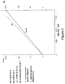
FIG. 3 shows diagram of Js vs Js′ and t vs t′ for normal n−p junction versus the depleted n−p junction.
FIG. 4 shows a vertical bipolar transistor of prior art.
FIG. 5 shows a vertical bipolar transistor with depleted emitter.
FIG. 6 shows a lateral bipolar transistor with depleted emitter.
FIG. 7 shows a vertical bipolar transistor with depleted emitter and base strips.
FIG. 8 shows an IGBT cell diagram of depleted emitter of the bipolar transistor.
DETAILED DESCRIPTION OF THE PREFERRED EMBODIMENT Embodiment One
FIG. 1A is a normal charge diagram of an abrupt n−p junction. The total area of qNd.times.xd1 at n region is equal to qNa.times.xa1 at p region. Where Nd is the doping concentration of the n region and xd1 is the charge distance of the n region. Where Na is the doping concentration of p region and xa2 is the charge distance of the p region. As the distance xd2 of n region becomes smaller by disclosed methods of the terminators, the total area of qNd.times.xd2 is smaller than qNd.times.xd1 with same doping level of Nd as shown in FIG. 1B. In order to balance the total charge, qNa.times.xa2 is the equal to qNd.times.xd2. Thus the built-in potential of FIG. 1B is smaller than the built-in potential of FIG. 1A. In order to get good ohmic contact, a very thin layer and heavily doped n type layer is placed at xd2 called the terminator. Otherwise a Schottky contact with reverse diode is connected to the n−p junction when the metallization is applied. The purpose of this terminator at xd2 is to terminate the n region and also to form the ohmic contact to the metallization. The same theory is also applied to p−n junction. The built-in potential of a normal n−p junction is ranging from less than 0.8 ev to over 0.9 ev for silicon material depending on the doping concentrations of the n−p junction. The depleted n−p junction has the built-in potential from below 0.9 ev to below 0.4 ev. The difference of the built-in potentials of the normal n−p junction to the depleted n−p junction is from lower than 0.01 ev to more than 0.40 ev.
FIG. 2A illuminates the doping concentration diagram of the abrupt n−p junction with normal n−p junction in solid lines versus the depleted n−p junction in dotted lines. As the n side of the n−p junction is terminated earlier by a terminator, the p side charge region will also terminated earlier in order to seek the charge balance. FIG. 2A shows a clear view of FIGS. 1A and 1B. The built-in potential is in the area shown in FIG. 2B. The vertical axis is the electric field and the maximum electric field located at x=0. The normal n−p junction has the built-in potential shown in the solid line triangle area and the depleted n−p junction is shown in dotted line triangle area. FIG. 2C shows the energy diagram of the n−p junction in equilibrium condition, the Fermi energy is shown in a flat dotted line and the conduction band of n type region is connected to the conduction band of p type region via the charge region in both sides of the junction and valence band is connected from the n type region to the valence band of p type region also via the charge region. The key concept to terminate the lightly doped region is to use very thin and heavily doped layer called a terminator to provide the ohmic contact to the metallization layer. This terminator is made by a thin layer of heavily doped region to connect to the fully depleted n type region by using low temperature diffusion or implant or via a very thin layer of poly film with heavily doping by low temperature diffusion without going through the depleted n region. Otherwise a Schottky contact with different polarity to the metallization layer could happen and can not achieve the requirement for a good p−n junction.
FIG. 3 shows the diagram of Js′/Js and t/t′ versus the difference of built-in potential in terms of ev for silicon material. The doping concentration of this Figure is Nd=2 E19 cm-3 and Na=1 E16 cm-3 for silicon material as used in this Figure as an example, the saturation current density is calculated as Js=8.93 E-12 A/cm2. When the n region (emitter) is terminated earlier in fully depleted mode, the depleted mode saturation current Js′ can be approximately shown as Js′=Js exp(q/kT(Vbi−Vbi′)) where Js is the saturation current density of the normal n−p junction of Nd=2 E19 cm-3 and Na=1 E16 cm-3. Vbi of 0.906 ev is calculated as the built-in potential of the normal n−p junction at room temperature and Vbi′ is the built-in potential of the depleted n−p junction as shown in FIG. 2B. In FIG. 3 t is the effective lifetime of the normal n−p junction and t′ is the effective lifetime of the depleted n−p junction. The x axis of FIG. 3 is the difference of the built-in potential of the normal n−p junction to the built-in potential of the depleted n−p junction. As x axis moves to right, the fully depleted n−p junction has smaller built-in potential, the space charge region is smaller, the effective life time becomes much smaller thus the bipolar transistor speed becomes faster. The saturation current density becomes larger when the built-in potential is smaller as shown in the equation and this diagram. Thus the depleted n−p junction can approach to Schottky rectifier's performance.
Embodiment Two
FIG. 4 shows a standard vertical bipolar transistor in the prior art. Layer 101 is a heavily doped substrate. Layer 100 is a lightly doped epitaxial layer with the same polarity as the substrate. Later 102 is the layer of opposite polarity of the epitaxial layer as the base of the bipolar transistor. Layer 103 is a heavily doped layer with the opposite polarity as the layer 102 and with the same polarity as the layer 100. Layer 104 is a heavily doped with the same polarity as the layer 102. This layer 104 serves as the ohmic contact to the base layer 102 and the metal layer 107 as the base terminal. Later 105 is the oxide layer to be formed either by thermal oxidation or CVD or both. Layer 106 is the metallization for the emitter contact. Layer 106 and layer 107 can be form either by Aluminum layer for wire bond or the NiAu layers on the top of Aluminum layer for the solder joint or other metallization layers. Layer 108 is a metallization layer that can be formed either by TiNiAg films, CrAu films or nickel plating. This layer 108 is used for the collector terminal to be soldered onto the package.
FIG. 5 is the same as the FIG. 4 except the layer 103A is a depleted region with the polarity opposite to the layer 102 as described in FIGS. 1, 2 and 3. This layer 103A can be higher, slightly high or even lower doping concentration with the opposite polarity to the layer 102. Layer 103A is very thin so that the depletion layer is fully depleted and in this condition the built-in voltage between emitter and the base is less than the full built-in potential as described in FIG. 2A. A terminator of very low implant energy and moderate dose to provide heavy surface concentration is implanted on the top of layer 103A to the emitter region. The implant dose for the region 103A is from 1.0 E11 to 1.0 E14 with the energy from less than 100V to over 10 KV. The terminator of 103A requires the implant dose from 1.0 E12 to 1.0 E15 with the implant energy from less than 100V to over 1000V. The terminator can also use low temperature diffusion with the same polarity of 103A from 700 deg C. to over 1100 deg C. with time from over two hours to less than 30 seconds. The implant anneal temperature can be performed from 1150 deg C. to 600 deg C. with time from less than 10 sec to 30 min. The terminator can also use a thin layer of poly silicon film on the top of 103A and completed by diffusion of low temperature or implant by low and moderate dose and energy described above. The thermal process of the terminator must not drive the doping to go through the layer 103A to become normal n+p junction. Due to fully depleted layer of 103A, the charge storage is thus reduced compared with n+p junction. With the reduced emitter to base charge, the transistor is thus faster compared with standard emitter to base junction as illustrated in FIGS. 2 and 3. The same theory also applies top type emitter to n type base junction.
Embodiment Three
FIG. 6 is a lateral bipolar transistor with depleted emitter region 103A. Layer 101 is a heavily doped with the different polarity with the substrate 102A and same polarity as the epi layer 100. The buried layer 101 is formed by diffusion before the epitaxial layer 100 deposition. The epitaxial layer 100 is the same polarity of the substrate 102A. The structure 101A is formed by deep diffusion of the same polarity as the epi layer 100. Layer 104 is a heavily doped layer with the same polarity as the layer 102 for the ohmic contact to the base region. The metallization of 106 and 107 is generally an Aluminum layer. The region 106 is the emitter, 107 is the base and 108 is the collector. This layer 103A can be higher, slightly high or even lower doping concentration with the opposite polarity to the layer 102. Layer 103A is very thin so that the depletion layer is fully depleted and in this condition the built-in voltage between emitter and the base is less than the full built-in potential as described in FIGS. 1A and 1B. A terminator of very low implant energy and moderate dose to provide heavy surface concentration is implanted on the top of layer 103A to the emitter region. The implant dose for the region 103A is from 1.0 E11 to 1.0 E14 with the energy from less than 100V to over 10 KV. The terminator of 103A requires the implant dose from 1.0 E12 to 1.0 E15 with the implant energy from less than 100V to over 1000V. The terminator can also use low temperature diffusion from 700 deg C. to over 1100 deg C. with time from over two hours to less than 30 seconds. The implant anneal temperature can be performed from 1150 deg C. to 600 deg C. from less than 10 sec to 30 min. The terminator can also use a thin layer of poly silicon film on the top of 103A and completed by diffusion of low temperature or implant by low and moderate dose and energy. The thermal process of the terminator must not drive the doping to go through the layer 103A to become normal n+p junction. Due to fully depleted layer of 103A, the charge storage is thus reduced compared with n+p junction. With the reduced emitter to base charge and capacitance, the transistor is thus faster compared with standard emitter to base junction as illustrated in FIGS. 2 and 3. The same theory also applies to p type emitter to n type base junction.
FIG. 7 is a novel structure of the bipolar transistor on the side view. The emitter region 103A is a fully depleted or incomplete region as shown in FIGS. 2 and 3. The base layer 102 is a strip structure (i.e. a broken base region) comprising a plurality of regions with the gap between any two neighboring regions small enough that the depletion layer of 102 in the epi region 100 is extended to cover this gap. When the base voltage is zero or negative voltage against the emitter and collector, this structure is looking like a standard bipolar transistor. When the base voltage is forward biased to the emitter and the collector, the transistor is looking like the JFET. This thus reduces the conduction resistance compared with the bipolar transistor. Since the reduction of the emitter to base capacitance and charge, this structure is faster than the comparable bipolar transistors.
The layer 102C is heavily doped region with the same polarity as the layer 102 for the ohmic contact to the base metal. Layer 107 is the base contact and 106 is used for the emitter contact. The metallization of 106 and 107 can be done by Aluminum layer for wire bond or with NiAu plating on the top of Aluminum for soldering bond. Layer 108 is the bottom metallization layer for the collector terminal. This metallization is generally to be done by TiNiAg, CrAu or by simple nickel plating. Again, the layer 103A can be higher, slightly high or even lower doping concentration with the opposite polarity to the layer 102. Layer 103A a depleted layer of emitter region and in this condition the built-in voltage between emitter and the base is less than the full built-in potential as described in FIG. 2A. A terminator of very low implant energy and moderate dose to provide heavy surface concentration is implanted on the top of layer 103A to the emitter region. The implant dose for the region 103A is from 1.0 E11 to 1.0 E14 with the energy from less than 100V to over 10 KV. The terminator of 103A requires the implant dose from 1.0 E12 to 1.0 E15 with the implant energy from less than 100V to over 1000V. The terminator can also use low temperature diffusion from 700 deg C. to over 1100 deg C. with time from over two hours to less than 30 seconds. The implant anneal temperature can be performed from 1150 deg C. to 600 deg C. from less than 10 sec to 30 min. The terminator can also use a thin layer of poly silicon film on the top of 103A and completed by diffusion of low temperature or implant by low and moderate dose and energy. The thermal process of the terminator must not drive the doping to go through the layer 103A to become normal n+p junction. Due to fully depleted layer of 103A, the charge storage is thus reduced compared with n+p junction. With the reduced emitter to base charge, the transistor is thus faster compared with standard emitter to base junction as illustrated in FIGS. 2 and 3. The same theory also applies to p type emitter to n type base junction.
Embodiment Four
FIG. 8 shows an IGBT cell structure with depleted emitter for the fast response. For example, the substrate 101 is a heavily doped p type material as the collector. Epitaxial layer 100 is served as the base which is in opposite polarity of the substrate 101. The gate region 105 can be a doped poly layer or a silicide layer. The gate oxide 106 can be formed by thermal oxidation and layer 106A is a CVD oxide to serve an insulation layer around the gate 105. Layer 102A is a depleted region with opposite polarity of the base region. The built-in potential of 102A to base 100 has lower built-in potential compared with the normal p−n junction. Thus the fast bipolar transistor speed can be reached. The layer 102 connected to layer 102A is a normal doped p region to serve as the base for the conduction channel of the MOSFET between the 103, n+, layer to the n type base or drift region. A thin and heavily doped terminator is place between 102A and the emitter metallization 107. The terminator is described in FIGS. 5, 6, and 7. The metallization layer 107 is usually a thick Aluminum layer for the wire bond or a layer of NiAu on top of Aluminum layer for the soldering. The metallization layer 108 can be TiNiAg, CrAu, or Ni plating for the soldering of the device to the package.

Claims (9)

1. A method for creating a depleted emitter of a bipolar transistor, comprising:
forming a base layer of said bipolar transistor with a first dopant of one polarity, wherein said base layer is eventually connected to a base terminal;
forming an emitter layer of said bipolar transistor with a second dopant above said base layer to create an emitter-base junction, wherein said second dopant having an opposite polarity to said first dopant;
forming a thin termination layer of heavy doping of said second dopant on top of said emitter layer by a thermal process, wherein said thermal process allows said dopant of the termination layer to stay within said emitter layer, such that said emitter-base junction does not become a normal n+-p or p+-n junction and the built-in potential of said emitter-base junction ranges from about 0.9 eV to about 0.4 eV; and
forming a metallization layer above said termination layer, wherein said termination layer can provide an ohmic contact to said metallization layer.
2. The method of claim 1, wherein said thermal process comprises:
performing an implant in said emitter layer with implant dose ranging from about 1.0 E11 to about 1.0 E14 and implant energy ranging from about 100 V to about 10 KV; and
Subsequently, performing an implant in said termination layer with implant dose from about 1.0 E12 to about 1.0 E15 and implant energy from about 100 V to about 1000 V.
3. The method of claim 1, wherein said thermal process comprises:
applying a low temperature diffusion with the same polarity as said emitter layer, wherein temperature ranges from about 700° C. to about 1100° C. with time ranging from about two hours to about 30 seconds.
4. The method of claim 1, wherein said thermal process comprises:
performing an implant anneal of said termination layer with temperature from about 1150° C. to about 600° C. and time from about 10 seconds to 30 minutes, and depositing a thin layer of poly silicon; and
subsequently applying a low temperature diffusion with temperature ranging from about 700° C. to about 1100° C. and time ranging from about two hours to about 30 seconds.
5. The method of claim 1, wherein said emitter-base junction can be applied to said bipolar transistor in either vertical or lateral device structure.
6. The method of claim 1, further comprising a lightly doped epitaxial layer of said second dopant below said base layer.
7. The method of claim 6, wherein said base layer further comprising a strip structure having a plurality of regions separated by gaps, wherein each gap between any two neighboring regions is substantially small to allow the depletion region between said base layer and said epitaxial layer to cover said corresponding gap.
8. The method of claim 7, wherein said gaps further allow said regions of said base layer to close current flow between emitter and collector of said bipolar transistor when base is in reverse bias against said emitter and said collector.
9. The method of claim 7, wherein said gaps further allow conduction paths to form between said regions of said base layer and behave like a Junction Field-Effect Transistor (JFET) when base is in forward bias against emitter and collector.
US11/804,229 2006-05-19 2007-05-17 Bipolar transistors with depleted emitter Expired - Fee Related US7795103B2 (en)

Priority Applications (2)

Application Number Priority Date Filing Date Title
US11/804,229 US7795103B2 (en) 2006-05-19 2007-05-17 Bipolar transistors with depleted emitter
US12/839,408 US7911033B2 (en) 2006-05-19 2010-07-20 Bipolar transistor with depleted emitter

Applications Claiming Priority (2)

Application Number Priority Date Filing Date Title
US80202706P 2006-05-19 2006-05-19
US11/804,229 US7795103B2 (en) 2006-05-19 2007-05-17 Bipolar transistors with depleted emitter

Related Child Applications (1)

Application Number Title Priority Date Filing Date
US12/839,408 Division US7911033B2 (en) 2006-05-19 2010-07-20 Bipolar transistor with depleted emitter

Publications (2)

Publication Number Publication Date
US20070267656A1 US20070267656A1 (en) 2007-11-22
US7795103B2 true US7795103B2 (en) 2010-09-14

Family

ID=38711214

Family Applications (2)

Application Number Title Priority Date Filing Date
US11/804,229 Expired - Fee Related US7795103B2 (en) 2006-05-19 2007-05-17 Bipolar transistors with depleted emitter
US12/839,408 Expired - Fee Related US7911033B2 (en) 2006-05-19 2010-07-20 Bipolar transistor with depleted emitter

Family Applications After (1)

Application Number Title Priority Date Filing Date
US12/839,408 Expired - Fee Related US7911033B2 (en) 2006-05-19 2010-07-20 Bipolar transistor with depleted emitter

Country Status (1)

Country Link
US (2) US7795103B2 (en)

Cited By (1)

* Cited by examiner, † Cited by third party
Publication number Priority date Publication date Assignee Title
US10304971B2 (en) 2016-07-16 2019-05-28 Champion Microelectronic Corp. High speed Schottky rectifier

Families Citing this family (4)

* Cited by examiner, † Cited by third party
Publication number Priority date Publication date Assignee Title
US20140073106A1 (en) 2012-09-12 2014-03-13 International Business Machines Corporation Lateral bipolar transistor and cmos hybrid technology
CN103296072B (en) * 2013-06-25 2016-08-10 江苏博普电子科技有限责任公司 A kind of bipolar transistor that improve BVcbo and production technology thereof
CN104377237A (en) * 2014-12-02 2015-02-25 杭州晶地半导体有限公司 Low-voltage IGBT thin crystal chip and preparation method thereof
CN108172622A (en) * 2018-01-30 2018-06-15 电子科技大学 Power semiconductor

Citations (7)

* Cited by examiner, † Cited by third party
Publication number Priority date Publication date Assignee Title
US4259680A (en) 1980-04-17 1981-03-31 Bell Telephone Laboratories, Incorporated High speed lateral bipolar transistor
US4483726A (en) 1981-06-30 1984-11-20 International Business Machines Corporation Double self-aligned fabrication process for making a bipolar transistor structure having a small polysilicon-to-extrinsic base contact area
US4581319A (en) 1983-08-26 1986-04-08 Siemens Aktiengesellschaft Method for the manufacture of bipolar transistor structures with self-adjusting emitter and base regions for extreme high frequency circuits
US4729965A (en) 1984-08-10 1988-03-08 Hitachi, Ltd. Method of forming extrinsic base by diffusion from polysilicon/silicide source and emitter by lithography
US5024957A (en) 1989-02-13 1991-06-18 International Business Machines Corporation Method of fabricating a bipolar transistor with ultra-thin epitaxial base
US5098854A (en) 1984-07-09 1992-03-24 National Semiconductor Corporation Process for forming self-aligned silicide base contact for bipolar transistor
US5101256A (en) 1989-02-13 1992-03-31 International Business Machines Corporation Bipolar transistor with ultra-thin epitaxial base and method of fabricating same

Patent Citations (7)

* Cited by examiner, † Cited by third party
Publication number Priority date Publication date Assignee Title
US4259680A (en) 1980-04-17 1981-03-31 Bell Telephone Laboratories, Incorporated High speed lateral bipolar transistor
US4483726A (en) 1981-06-30 1984-11-20 International Business Machines Corporation Double self-aligned fabrication process for making a bipolar transistor structure having a small polysilicon-to-extrinsic base contact area
US4581319A (en) 1983-08-26 1986-04-08 Siemens Aktiengesellschaft Method for the manufacture of bipolar transistor structures with self-adjusting emitter and base regions for extreme high frequency circuits
US5098854A (en) 1984-07-09 1992-03-24 National Semiconductor Corporation Process for forming self-aligned silicide base contact for bipolar transistor
US4729965A (en) 1984-08-10 1988-03-08 Hitachi, Ltd. Method of forming extrinsic base by diffusion from polysilicon/silicide source and emitter by lithography
US5024957A (en) 1989-02-13 1991-06-18 International Business Machines Corporation Method of fabricating a bipolar transistor with ultra-thin epitaxial base
US5101256A (en) 1989-02-13 1992-03-31 International Business Machines Corporation Bipolar transistor with ultra-thin epitaxial base and method of fabricating same

Cited By (1)

* Cited by examiner, † Cited by third party
Publication number Priority date Publication date Assignee Title
US10304971B2 (en) 2016-07-16 2019-05-28 Champion Microelectronic Corp. High speed Schottky rectifier

Also Published As

Publication number Publication date
US7911033B2 (en) 2011-03-22
US20070267656A1 (en) 2007-11-22
US20100283082A1 (en) 2010-11-11

Similar Documents

Publication Publication Date Title
JP3291957B2 (en) Vertical trench MISFET and method of manufacturing the same
JP2623850B2 (en) Conductivity modulation type MOSFET
US8003991B2 (en) Silicon carbide MOS field effect transistor with built-in Schottky diode and method for fabrication thereof
JP2995723B2 (en) Vertical current semiconductor device using wafer bonding and method of manufacturing the same
KR100854078B1 (en) MOS gated power semiconductor device and method for fabricating the same
US4607270A (en) Schottky barrier diode with guard ring
US7847315B2 (en) High efficiency rectifier
TW201246537A (en) Field effect transistor devices with low source resistance
US10147813B2 (en) Tunneling field effect transistor
US7911033B2 (en) Bipolar transistor with depleted emitter
US7164160B2 (en) Integrated circuit device with a vertical JFET
US6448588B2 (en) Insulated gate bipolar transistor having high breakdown voltage in reverse blocking mode
JPS6252469B2 (en)
JP2001127285A (en) Vertical field-effect transistor
JP3673334B2 (en) Semiconductor diode
JPH0494576A (en) Vertical power mos fet
JP2808871B2 (en) Method for manufacturing MOS type semiconductor device
JPS63124580A (en) Construction of high dielectric strength p-n junction and method of forming the same
JPS5924550B2 (en) semiconductor equipment
US6855983B1 (en) Semiconductor device having reduced on resistance
JPH0493083A (en) Semiconductor device and manufacture thereof
JP3210146B2 (en) Semiconductor device
US20220115532A1 (en) Power semiconductor device and manufacturing method therefor
JPH0480970A (en) Insulated-gate field-effect transistor
JPH11307657A (en) Semiconductor integrated circuit

Legal Events

Date Code Title Description
STCF Information on status: patent grant

Free format text: PATENTED CASE

FPAY Fee payment

Year of fee payment: 4

FEPP Fee payment procedure

Free format text: MAINTENANCE FEE REMINDER MAILED (ORIGINAL EVENT CODE: REM.)

FEPP Fee payment procedure

Free format text: 7.5 YR SURCHARGE - LATE PMT W/IN 6 MO, SMALL ENTITY (ORIGINAL EVENT CODE: M2555); ENTITY STATUS OF PATENT OWNER: SMALL ENTITY

MAFP Maintenance fee payment

Free format text: PAYMENT OF MAINTENANCE FEE, 8TH YR, SMALL ENTITY (ORIGINAL EVENT CODE: M2552); ENTITY STATUS OF PATENT OWNER: SMALL ENTITY

Year of fee payment: 8

FEPP Fee payment procedure

Free format text: MAINTENANCE FEE REMINDER MAILED (ORIGINAL EVENT CODE: REM.); ENTITY STATUS OF PATENT OWNER: SMALL ENTITY

LAPS Lapse for failure to pay maintenance fees

Free format text: PATENT EXPIRED FOR FAILURE TO PAY MAINTENANCE FEES (ORIGINAL EVENT CODE: EXP.); ENTITY STATUS OF PATENT OWNER: SMALL ENTITY

STCH Information on status: patent discontinuation

Free format text: PATENT EXPIRED DUE TO NONPAYMENT OF MAINTENANCE FEES UNDER 37 CFR 1.362

FP Lapsed due to failure to pay maintenance fee

Effective date: 20220914