US7791189B2 - Multipiece apparatus for thermal and electromagnetic interference (EMI) shielding enhancement in die-up array packages and method of making the same - Google Patents
Multipiece apparatus for thermal and electromagnetic interference (EMI) shielding enhancement in die-up array packages and method of making the same Download PDFInfo
- Publication number
- US7791189B2 US7791189B2 US12/352,309 US35230909A US7791189B2 US 7791189 B2 US7791189 B2 US 7791189B2 US 35230909 A US35230909 A US 35230909A US 7791189 B2 US7791189 B2 US 7791189B2
- Authority
- US
- United States
- Prior art keywords
- stiffener
- die
- frame body
- substrate
- package
- Prior art date
- Legal status (The legal status is an assumption and is not a legal conclusion. Google has not performed a legal analysis and makes no representation as to the accuracy of the status listed.)
- Expired - Fee Related
Links
Images


Classifications
-
- H—ELECTRICITY
- H10—SEMICONDUCTOR DEVICES; ELECTRIC SOLID-STATE DEVICES NOT OTHERWISE PROVIDED FOR
- H10W—GENERIC PACKAGES, INTERCONNECTIONS, CONNECTORS OR OTHER CONSTRUCTIONAL DETAILS OF DEVICES COVERED BY CLASS H10
- H10W76/00—Containers; Fillings or auxiliary members therefor; Seals
- H10W76/40—Fillings or auxiliary members in containers, e.g. centering rings
- H10W76/42—Fillings
- H10W76/47—Solid or gel fillings
-
- H—ELECTRICITY
- H10—SEMICONDUCTOR DEVICES; ELECTRIC SOLID-STATE DEVICES NOT OTHERWISE PROVIDED FOR
- H10W—GENERIC PACKAGES, INTERCONNECTIONS, CONNECTORS OR OTHER CONSTRUCTIONAL DETAILS OF DEVICES COVERED BY CLASS H10
- H10W40/00—Arrangements for thermal protection or thermal control
- H10W40/70—Fillings or auxiliary members in containers or in encapsulations for thermal protection or control
- H10W40/77—Auxiliary members characterised by their shape
- H10W40/778—Auxiliary members characterised by their shape in encapsulations
-
- H—ELECTRICITY
- H10—SEMICONDUCTOR DEVICES; ELECTRIC SOLID-STATE DEVICES NOT OTHERWISE PROVIDED FOR
- H10W—GENERIC PACKAGES, INTERCONNECTIONS, CONNECTORS OR OTHER CONSTRUCTIONAL DETAILS OF DEVICES COVERED BY CLASS H10
- H10W42/00—Arrangements for protection of devices
- H10W42/20—Arrangements for protection of devices protecting against electromagnetic or particle radiation, e.g. light, X-rays, gamma-rays or electrons
-
- H—ELECTRICITY
- H10—SEMICONDUCTOR DEVICES; ELECTRIC SOLID-STATE DEVICES NOT OTHERWISE PROVIDED FOR
- H10W—GENERIC PACKAGES, INTERCONNECTIONS, CONNECTORS OR OTHER CONSTRUCTIONAL DETAILS OF DEVICES COVERED BY CLASS H10
- H10W74/00—Encapsulations, e.g. protective coatings
- H10W74/10—Encapsulations, e.g. protective coatings characterised by their shape or disposition
- H10W74/111—Encapsulations, e.g. protective coatings characterised by their shape or disposition the semiconductor body being completely enclosed
- H10W74/114—Encapsulations, e.g. protective coatings characterised by their shape or disposition the semiconductor body being completely enclosed by a substrate and the encapsulations
- H10W74/117—Encapsulations, e.g. protective coatings characterised by their shape or disposition the semiconductor body being completely enclosed by a substrate and the encapsulations the substrate having spherical bumps for external connection
-
- H—ELECTRICITY
- H10—SEMICONDUCTOR DEVICES; ELECTRIC SOLID-STATE DEVICES NOT OTHERWISE PROVIDED FOR
- H10W—GENERIC PACKAGES, INTERCONNECTIONS, CONNECTORS OR OTHER CONSTRUCTIONAL DETAILS OF DEVICES COVERED BY CLASS H10
- H10W72/00—Interconnections or connectors in packages
- H10W72/50—Bond wires
- H10W72/531—Shapes of wire connectors
- H10W72/536—Shapes of wire connectors the connected ends being ball-shaped
-
- H—ELECTRICITY
- H10—SEMICONDUCTOR DEVICES; ELECTRIC SOLID-STATE DEVICES NOT OTHERWISE PROVIDED FOR
- H10W—GENERIC PACKAGES, INTERCONNECTIONS, CONNECTORS OR OTHER CONSTRUCTIONAL DETAILS OF DEVICES COVERED BY CLASS H10
- H10W72/00—Interconnections or connectors in packages
- H10W72/50—Bond wires
- H10W72/531—Shapes of wire connectors
- H10W72/5363—Shapes of wire connectors the connected ends being wedge-shaped
-
- H—ELECTRICITY
- H10—SEMICONDUCTOR DEVICES; ELECTRIC SOLID-STATE DEVICES NOT OTHERWISE PROVIDED FOR
- H10W—GENERIC PACKAGES, INTERCONNECTIONS, CONNECTORS OR OTHER CONSTRUCTIONAL DETAILS OF DEVICES COVERED BY CLASS H10
- H10W72/00—Interconnections or connectors in packages
- H10W72/50—Bond wires
- H10W72/541—Dispositions of bond wires
- H10W72/547—Dispositions of multiple bond wires
- H10W72/5473—Dispositions of multiple bond wires multiple bond wires connected to a common bond pad
-
- H—ELECTRICITY
- H10—SEMICONDUCTOR DEVICES; ELECTRIC SOLID-STATE DEVICES NOT OTHERWISE PROVIDED FOR
- H10W—GENERIC PACKAGES, INTERCONNECTIONS, CONNECTORS OR OTHER CONSTRUCTIONAL DETAILS OF DEVICES COVERED BY CLASS H10
- H10W72/00—Interconnections or connectors in packages
- H10W72/851—Dispositions of multiple connectors or interconnections
- H10W72/874—On different surfaces
- H10W72/884—Die-attach connectors and bond wires
-
- H—ELECTRICITY
- H10—SEMICONDUCTOR DEVICES; ELECTRIC SOLID-STATE DEVICES NOT OTHERWISE PROVIDED FOR
- H10W—GENERIC PACKAGES, INTERCONNECTIONS, CONNECTORS OR OTHER CONSTRUCTIONAL DETAILS OF DEVICES COVERED BY CLASS H10
- H10W74/00—Encapsulations, e.g. protective coatings
-
- H—ELECTRICITY
- H10—SEMICONDUCTOR DEVICES; ELECTRIC SOLID-STATE DEVICES NOT OTHERWISE PROVIDED FOR
- H10W—GENERIC PACKAGES, INTERCONNECTIONS, CONNECTORS OR OTHER CONSTRUCTIONAL DETAILS OF DEVICES COVERED BY CLASS H10
- H10W90/00—Package configurations
- H10W90/701—Package configurations characterised by the relative positions of pads or connectors relative to package parts
- H10W90/731—Package configurations characterised by the relative positions of pads or connectors relative to package parts of die-attach connectors
- H10W90/734—Package configurations characterised by the relative positions of pads or connectors relative to package parts of die-attach connectors between a chip and a stacked insulating package substrate, interposer or RDL
-
- H—ELECTRICITY
- H10—SEMICONDUCTOR DEVICES; ELECTRIC SOLID-STATE DEVICES NOT OTHERWISE PROVIDED FOR
- H10W—GENERIC PACKAGES, INTERCONNECTIONS, CONNECTORS OR OTHER CONSTRUCTIONAL DETAILS OF DEVICES COVERED BY CLASS H10
- H10W90/00—Package configurations
- H10W90/701—Package configurations characterised by the relative positions of pads or connectors relative to package parts
- H10W90/751—Package configurations characterised by the relative positions of pads or connectors relative to package parts of bond wires
- H10W90/754—Package configurations characterised by the relative positions of pads or connectors relative to package parts of bond wires between a chip and a stacked insulating package substrate, interposer or RDL
Definitions
- the invention relates generally to the field of integrated circuit (IC) device packaging technology and, more particularly to thermal enhancement and electromagnetic interference (EMI) shielding in IC device packages.
- IC integrated circuit
- EMI electromagnetic interference
- IC semiconductor dies are typically mounted in or on a package that is attached to a printed circuit board (PCB).
- Example IC device packages include ball grid array (BGA), pin grid array (PGA), and land grid array (LGA) packages.
- BGA ball grid array
- PGA pin grid array
- LGA land grid array
- a conventional BGA package has an array of solder balls located on a bottom external surface of a package substrate. The solder balls are reflowed to attach the package to the PCB.
- the IC die is typically mounted to a top surface of the package substrate. Wire bonds typically couple signals of the IC die to the substrate.
- the substrate has internal routing that electrically couples the signals of the IC die to the solder balls on the bottom substrate surface.
- a molding compound encapsulates the IC die, wire bonds, and the entire or partial top surface of the substrate to provide environmental protection.
- die-up and die-down BGA package configurations exist.
- the IC die In die-up BGA packages, the IC die is mounted on the top surface of the substrate, so that the active surface of the IC die is directed away from the PCB.
- die-down BGA packages the IC die is mounted on the bottom surface of the substrate, so that the active surface of the IC die is directed towards the PCB.
- Resin substrates and plastic molding compounds have low thermal conductivity values (e.g., about 0.19-0.3 W/m ⁇ ° C. for typical resin substrates, and about 0.2-0.9 W/m ⁇ ° C. for typical molding compounds).
- thermal conductivity values e.g., about 0.19-0.3 W/m ⁇ ° C. for typical resin substrates, and about 0.2-0.9 W/m ⁇ ° C. for typical molding compounds.
- a die-up array IC device package that provides enhanced ability to dissipate heat generated by the IC die, and shields EMI emanating from the IC die, as well as EMI radiating toward the IC die from outside the package.
- the present invention is directed to an apparatus and method for enhancing thermal performance and electromagnetic interference (EMI) shielding in die-up array integrated circuit (IC) device packages.
- EMI electromagnetic interference
- a die-up array IC device package includes a stiffener having opposing first and second surfaces, and an IC die mounted to the first surface of the stiffener.
- the package further includes a cap body having opposing first and second surfaces. A first portion of the second surface has a cavity formed therein, and a planar second portion of the second surface is coupled to the first surface of the stiffener.
- the package further includes a substrate having a first surface coupled to the second surface of the stiffener. A plurality of contact pads on the first surface are electrically connected through the substrate to an array of electrically conductive terminals on a second surface of the substrate.
- the stiffener and the cap body form an enclosure that substantially encloses the IC die.
- the die enclosure spreads heat from the IC die during operation of the IC die. Additionally or alternatively, the die enclosure shields EMI emanating from the IC die, as well as EMI radiating toward the IC die from outside the package.
- At least one tab protrudes from the second surface of the frame body. At least one receptacle formed in the first surface of the stiffener corresponding to the at least one tab. The at least one tab is coupled with the at least one corresponding receptacle, whereby structural coupling of said frame body to said stiffener is substantially improved.
- a die-up array IC device package in another embodiment, includes a stiffener having opposing first and second surfaces, and an IC die mounted to the first surface of the stiffener.
- the package further includes a cap body having opposing first and second surfaces. A first portion of the second surface has a cavity formed therein, and a planar second portion of the second surface is coupled to the first surface of the stiffener.
- the package further includes a substrate having a first surface coupled to the second surface of the stiffener. A plurality of contact pads on the first surface are electrically connected through the substrate to an array of electrically conductive terminals on a second surface of the substrate.
- the stiffener and the cap body form an enclosure that substantially encloses the IC die.
- the die enclosure spreads heat from the IC die during operation of the IC die. Additionally or alternatively, the die enclosure shields EMI emanating from the IC die, as well as EMI radiating toward the IC die from outside the package.
- the package further includes a heat sink coupled to the first surface of the lid.
- FIG. 1 illustrates a cross-sectional view of a conventional ball grid array (BGA) package.
- BGA ball grid array
- FIGS. 2 and 3 illustrate cross-sectional views of conventional BGA packages with drop-in heat spreaders.
- FIGS. 4 and 5 illustrate cross-sectional views of conventional BGA packages with enhanced thermal properties.
- FIG. 6A illustrates a cross-sectional view of a die-up BGA package, in accordance with an embodiment of the present invention, having a cap structure integrated with a stiffener.
- FIG. 6B illustrates the cap structure of FIG. 6A , in accordance with an embodiment of the present invention.
- FIGS. 7A and 7B illustrate top views of one-piece stiffener configurations having plated areas, in accordance with embodiments of the present invention.
- FIG. 7C illustrates a top view of a two-piece stiffener configuration having a plated area, in accordance with an embodiment of the present invention.
- FIGS. 8A and 8B illustrate a cross-sectional view and bottom view, respectively, of a cap structure with protruding tab members, in accordance with an embodiment of the present invention.
- FIGS. 9A-9C illustrate top views of a stiffener with receptacles formed in a surface, in accordance with embodiments of the present invention.
- FIG. 10 illustrates a cross-sectional view of a BGA package, in accordance with an embodiment of the present invention, with a cap structure having tab members coupled with corresponding receptacles in a stiffener.
- FIG. 11 illustrates a cross-sectional view of a BGA package, in accordance with an embodiment of the present invention, with mold gate openings through a cap structure, which has a surface not covered by an encapsulating material.
- FIG. 12 illustrates a cross-sectional view of a BGA package, in accordance with an embodiment of the present invention, with mold gate openings through a cap structure, which is covered by an encapsulating material.
- FIG. 13 illustrates a bottom view of a cap structure, in accordance with an embodiment of the present invention, with mold gate openings through a surface.
- FIG. 14 illustrates a cross-sectional view of a BGA package, in accordance with an embodiment of the present invention, with an encapsulating material covering a stiffener, which has a peripheral dimension that exceeds a peripheral dimension of a cap structure.
- FIG. 15 illustrates a cross-sectional view of a BGA package, in accordance with an embodiment of the present invention, with a die that is encapsulated by mold injection encapsulation.
- FIG. 16 illustrates a cross-sectional view of a BGA package, in accordance with an embodiment of the present invention, with a die that is encapsulated by dam-and-fill encapsulation.
- FIG. 17 illustrates a cross-sectional view of a BGA package, in accordance with an embodiment of the present invention, having a die encapsulated by mold injection encapsulation and a pressure release opening through a cap structure.
- FIG. 18 illustrates a cross-sectional view of a BGA package, in accordance with an embodiment of the present invention, having a die encapsulated by dam-and-fill encapsulation and a pressure release opening through a cap structure.
- FIG. 19 illustrates a cross-sectional view of a BGA package, in accordance with an embodiment of the present invention, having a cap structure with a pressure release opening.
- FIGS. 20-24 illustrate cross-sectional views of BGA packages, in accordance with embodiments of the present invention, configured with enhanced thermal properties.
- FIG. 25A illustrates a cross-sectional view of a BGA package, in accordance with an embodiment of the present invention, having a can structure integrated with a stiffener.
- FIG. 25B illustrates the can structure of FIG. 25A , in accordance with an embodiment of the present invention.
- FIG. 26 illustrates a cross-sectional view of a BGA package, in accordance with an embodiment of the present invention, having ring and lid structures integrated with a stiffener.
- FIG. 27 illustrates a perspective view of a ring structure with a groove formed in a surface, in accordance with an embodiment of the present invention.
- FIGS. 28-29 illustrate cross-sectional views of BGA packages, in accordance with embodiments of the present invention, having lid structures recess-mounted on ring structures.
- FIGS. 30-33 show flowcharts providing example steps for assembling a die-up array integrated circuit (IC) device package with enhanced thermal and electromagnetic interference (EMI) shielding properties, according to embodiments of the present invention.
- IC integrated circuit
- EMI electromagnetic interference
- FIG. 34 illustrates a cross-sectional view of a BGA package,in accordance with an embodiment of the present invention, having ring and lid structures integrated with a stiffener.
- a die-up array IC device package includes a plurality of electrically conductive terminals (e.g., solder balls, pins, pads, etc.) arranged in an array (e.g., columns and rows) on a bottom surface of a substrate. Signals from an IC die mounted on a top surface of the substrate are routed through the substrate to the electrically conductive terminals.
- the electrically conductive terminals are configured to be attached to a printed circuit board (PCB).
- PCB printed circuit board
- Examples of die-up array packages include BGA (e.g., pad array carrier, pad array package, land grid array, pad grid array packages), pin grid array, etc.
- a die-up array-type IC device package includes an IC die mounted to a first surface of a stiffener, and a package substrate coupled to a second surface of the stiffener.
- the package further includes a cap structure that has a cavity formed therein. The cap structure is coupled to the first surface of the stiffener so that the stiffener and the cap structure form an enclosure, which substantially encloses the IC die.
- the die enclosure forms a thermally conductive path from the IC die to the outer surfaces of the package for enhanced heat spreading. Additionally, or in alternative embodiments, the die enclosure shields EMI emanating from the IC die, as well as EMI radiating toward the IC die from outside the package. Furthermore, in embodiments, the die enclosure can be coupled to a voltage to form an electrical potential plane (e.g., a voltage plane or a ground plane) surrounding the IC die for enhanced EMI shielding. The die enclosure also enhances rigidity and improves planarity of the printed circuit substrate, and protects the IC die from the environment (e.g., chemical corrosives, moisture, heat, vibration, and mechanical impact, etc.). Optional lock-in mechanisms on the cap structure and the stiffener (referred to herein as “protruding tabs” and “receptacles,” respectively) can further enhance the thermal, electrical, and mechanical integrity of the die enclosure.
- an electrical potential plane e.g., a voltage plane or a ground plane
- the die enclosure
- the cap structure can have various configurations. For example, described herein are a one-piece cap structure with a trapezoidal cavity and a rim, and a one-piece cap structure with a rectangular cavity and no rim (referred to herein as a “can” structure). Also described herein is a multiple-piece cap structure that has a frame-shaped portion, which is coupled to the stiffener, and a planar portion, which is coupled to the frame-shaped portion (the frame-shaped and planar portions are referred to herein as “ring” and “lid” structures, respectively). The invention is not, however, limited to these example cap structure configurations.
- cap structure can also be referred to as “heat spreader” or a “drop-in heat spreader,” when used for thermal spreading.
- the stiffener can be patterned in different forms (e.g., openings, cutouts, steps, etc.) or shapes (e.g., square, rectangular, circular, spoke-like, cutouts or notches and steps on one or more edges, etc.) to facilitate wire bond interconnects and to enhance package performance.
- the stiffener can also be finished using a variety of processes, materials, and methodologies at various surfaces, spots, and locations. Openings can be formed through the stiffener to facilitate electrical interconnects between the IC die and the substrate, and the stiffener and the substrate.
- Example materials for the cap structure and the stiffener include copper, aluminum, aluminum based alloys, copper based alloys, ferromagnetic materials, laminated copper/iron, other metal and combinations of metals/alloys, other thermally and electrically conductive materials (e.g., ceramics, metallized plastics, etc.), and materials described elsewhere herein.
- Conventional types of substrate e.g., organic, tape, and ceramic, etc.
- advanced types of substrate e.g., high density substrate, build-up substrate, Teflon substrate, etc.
- Single routing layer substrates, as well as multiple routing layer substrates can also be used.
- FIG. 1 illustrates a cross-sectional view of a conventional BGA package 100 with an IC semiconductor die 115 mounted on a printed circuit substrate 110 , and a plastic molding compound 105 that encapsulates IC die 115 .
- Heat generated by IC die 115 can be trapped within BGA package 100 because materials for plastic molding compound 105 and dielectric materials, such as resin epoxy or polyimide tape, for substrate 110 have low thermal conductivity.
- BGA package 100 does not provide EMI shielding because materials for plastic molding compound 105 and dielectric materials, such as resin epoxy or polyimide tape, for substrate 110 are transparent to EMI.
- FIG. 2 illustrates a cross-sectional view of a conventional BGA package 200 with an IC semiconductor die 215 mounted on a printed circuit substrate 210 and encapsulated by a mold compound 205 .
- BGA package 200 includes a drop-in heat spreader 220 to promote dissipation of heat within plastic molding compound 205 .
- direct contact between IC die 215 and heat spreader 220 is not permitted in package 200 . This is required to avoid shorting heat spreader 220 with the active surface of IC die 215 and wire bond interconnections 225 .
- heat generated by IC die 215 must pass through plastic molding compound 205 in order to reach heat spreader 220 , and can therefore remain trapped within BGA package 200 .
- drop-in heat spreader 220 only provides limited EMI shielding, if any.
- EMI generated outside BGA package 200 can penetrate printed circuit substrate 210 and interfere with the operation of IC die 215 .
- EMI generated by IC die 215 can escape through trace metal openings or gaps in printed circuit substrate 210 to outside BGA package 200 .
- FIG. 3 illustrates a cross-sectional view of a conventional BGA package 300 , similar to BGA package 200 , but with a differently configured heat spreader 320 .
- BGA package 300 suffers from the same thermal and electromagnetic shielding deficiencies as BGA package 200 .
- a plastic molding compound 305 and a printed circuit substrate 310 trap heat generated by an IC die 315 within BGA package 300 , and EMI generated inside and outside of BGA package 300 can penetrate printed circuit substrate 310 .
- FIGS. 4 and 5 illustrate cross-sectional views of further conventional BGA packages.
- FIG. 4 illustrates a BGA package 400 with a metal stiffener 420 that has a larger surface area than an IC die 415 to promote heat dissipation into surrounding materials.
- Metal stiffener 420 is attached to an organic substrate 410 , such as a polyimide tape or resin epoxy substrate.
- FIG. 5 illustrates a cross-sectional view of a BGA package 500 , which provides a thermal and electrical connection between an IC die 515 and a printed circuit board (PCB) (not shown) through a metal heat slug 525 .
- PCB printed circuit board
- FIG. 5 illustrates a cross-sectional view of a BGA package 500 , which provides a thermal and electrical connection between an IC die 515 and a printed circuit board (PCB) (not shown) through a metal heat slug 525 .
- PCB printed circuit board
- Metal stiffeners 420 and 520 of BGA packages 400 and 500 shield EMI radiating toward IC dies 415 and 515 from the area underneath the IC dies.
- BGA packages 400 and 500 do not shield EMI radiating towards IC dies 415 and 515 from the area above the active surface of the IC dies.
- BGA packages 400 and 500 also do not prevent EMI emanating from IC dies 415 and 515 from escaping the package through the area above the active surface of the IC dies.
- FIG. 6A illustrates a cross-sectional view of a die-up BGA package 600 , in accordance with an embodiment of the present invention.
- BGA package 600 provides for enhanced heat spreading and EMI shielding.
- BGA package 600 includes a printed circuit substrate 610 , a stiffener 620 , and a cap body 625 .
- An IC die 615 is mounted to a center region of a first surface 621 of stiffener 620 with a die attach material 624 , such as an epoxy or solder.
- Cap body 625 is coupled to first surface 621 of stiffener 620 , forming a die enclosure 680 that substantially surrounds IC die 615 .
- a second surface 622 of stiffener 620 is attached to a first surface 611 of substrate 610 .
- a plurality of solder balls 613 is coupled to a second surface 612 of substrate 610 . Solder balls 613 are reflowed to attach package 600 to a PCB
- BGA package 600 further includes openings 635 , wire bonds 640 , 650 , and 655 , and mold compound 605 .
- Openings 635 formed in stiffener 620 facilitate interconnection of one or more wire bonds 640 between corresponding pads 645 on IC die 615 and substrate 610 .
- Pads 645 can be any type of signal pads of IC die 615 , including I/O pads, voltage pads, ground pads, etc.
- Openings 635 also facilitate interconnection of one or more wire bonds 655 between stiffener 620 and substrate 610 (e.g., traces, contacts, ground rings, ground planes, voltage planes, etc. of substrate 610 ).
- One or more wire bonds 650 couple corresponding pads 646 on IC die 615 to stiffener 620 .
- Pads 646 can be any type of signal pads of IC die 615 , such as I/O pads, voltage pads, ground pads, etc.
- a mold compound 605 encapsulates IC die 615 and wire bonds 640 , 650 , and 655 .
- FIG. 6B illustrates a cross-sectional view of cap body 625 , shown in FIG. 6A , in accordance with an embodiment of the present invention.
- cap body 625 has a planar top portion 660 , planar sidewall portions 685 , and a rim 665 extending around a bottom periphery of cap body 625 .
- Sidewall portions 685 couple top portion 660 to rim 665 , and are angled outward from top portion 660 .
- top portion 660 and sidewall surfaces 685 are shown as planar but can also be non-planar (e.g., curved, or other shapes).
- Cap body 625 further has a first surface 690 and a second surface 691 .
- a portion of first surface 690 is exposed through mold compound 605 , as shown in FIG. 6A .
- Second surface 691 has cavity 630 formed therein. Cavity 630 is shown in FIG. 6B as having a trapezoidal shaped cross-section, but can have other shapes, including rectangular, etc.
- Second surface 691 of cap body 625 (at rim 665 ) is coupled to stiffener 620 , as shown in FIG. 6A .
- Example materials for substrate 610 include organic (e.g., BT, FR4, etc.), ceramic, glass, tape, and other materials.
- Substrate 610 can have one or more electrical routing layers, which are constructed through lamination, build-up, or other processes.
- Example materials for stiffener 620 and cap body 625 include copper, aluminum, aluminum based alloys, copper based alloys, ferromagnetic materials, laminated copper/iron, other metals and combinations of metals/alloys, other thermally and electrically conductive materials (e.g., ceramics, metallized plastics, etc.), and other materials described elsewhere herein.
- Stiffener 620 and cap body 625 can be made of the same material or different materials.
- Stiffener 620 can have any thickness, depending on the particular application. For example, in embodiments, stiffener 620 can have a thickness anywhere in the range of 0.01 mm to 10 mm.
- stiffener 620 can have a thickness in the range of about 0.1 mm to about 0.5 mm. In another example embodiment, stiffener 620 can have a thickness of about 1.17 mm.
- cap body 625 can have any thickness, depending on the particular application. For example, in embodiments, cap body 625 can have a thickness anywhere in the range of 0.01 mm to 10 mm. In an example embodiment, cap body can have a thickness in the range of about 0.1 mm to about 1.0 mm.
- surfaces of stiffener 620 can be finished or un-finished.
- surfaces of stiffener 620 can be finished using processes such as micro-etch or oxidation to promote adhesion with mold compound 605 .
- first surface 621 of stiffener 620 can be patterned (e.g. spot, strip, bar, ring, other shapes) with one or more electrically conductive plated areas (e.g., silver, solder, nickel, gold, metal combinations/alloys, etc.) for enhanced coupling of wire bonds 650 to first surface 621 .
- Stiffener 620 can also be patterned in various forms to improve package mechanical, thermal, and electrical performances and package reliability. (See, e.g. U.S. patent application Ser. No.
- notches/cutouts and steps can be patterned on the edges of stiffener 620 to reduce a length of wire bond 640 between IC die 615 and substrate 610 , improve substrate 610 routability, and improve manufacturing processes.
- die enclosure 680 When stiffener 620 and cap body 625 are coupled together, as shown in FIG. 6A , die enclosure 680 is formed. Die enclosure 680 shields EMI emanating from IC die 615 , as well as EMI radiating toward IC die 615 from outside package 600 . In order to provide enhanced EMI protection, die enclosure 680 can be coupled to a ground potential (e.g., to create a Faraday cage), or to other electrical potentials (i.e., to create a voltage plane). When stiffener 620 is coupled with ground pads 646 (or bond pads of other electrical potentials) on IC die 615 , die enclosure 680 operates as a ground potential (or other electrical potential) plane for IC die 615 . Furthermore, this ground potential plane can be externally accessed at first surface 690 of top portion 660 of cap body 625 , if desired.
- a ground potential e.g., to create a Faraday cage
- other electrical potentials i.e., to create a voltage plane
- electrically conductive adhesives such as epoxy filled with silver particles or flakes, can be used to couple cap body 625 to stiffener 620 .
- Soldering materials such as tin-lead or silver, can also be used to couple cap body 625 to stiffener 620 through processes such as solder plating and reflow or screen printing of paste and reflow.
- thermally conductive adhesives can be used to enhance thermal contact between cap body 625 and stiffener 620 .
- FIGS. 7A-7C show example configurations for stiffener 620 , according to embodiments of the present invention.
- Thermally and/or electrically conductive materials e.g., silver, solder, nickel, gold, metal combinations/alloys, etc.
- FIG. 7A illustrates a top view of a one-piece stiffener 702 with a plurality of wire bond openings 705 and a plated ring-shaped area 710 .
- wire bond openings 705 can be trapezoidal shaped, although openings 705 can have other shapes, including rectangular, oval, etc.
- Ring area 710 is plated with an electrically conductive material to enhance electrical contact with cap body 625 .
- FIG. 7B illustrates a top view of a one-piece stiffener 704 with a trapezoidal wire bond opening 705 , multiple cutouts 725 , and plated areas 730 , 735 , and 740 .
- Cutouts 725 are recessed edge portions of stiffener 620 . Cutouts 725 can be used to allow wire bond connections between an IC die and a package substrate in the areas of cutouts 725 .
- Areas 730 , 735 , and 740 are plated with an electrically conductive material. Area 730 has an elongated strip shape, area 735 is circular, and area 740 is rectangular. Note that plated areas can have alternative shapes and/or sizes. Areas 730 , 735 , and 740 can be used to enhance electrical contact with cap body 625 .
- FIG. 7C illustrates a top view of a two-piece stiffener 706 , with a first stiffener portion 765 separated by a channel 755 from a second stiffener portion 760 .
- Two-piece stiffener 706 of FIG. 7C includes wire bond openings 750 , 751 , and 752 , through first stiffener portion 765 .
- a plated U-shaped area 770 is patterned on first stiffener portion 765 .
- wire bond openings 750 , 751 , and 752 can be rectangular shaped, although, openings 750 , 751 , and 752 can have other shapes (e.g., trapezoidal, etc.).
- U-shaped area 770 is plated with an electrically conductive material to enhance electrical contact with cap body 625 .
- second stiffener portion 760 is electrically isolated from first stiffener portion 765 by channel 755 .
- second stiffener portion 760 is also electrically isolated from cap body 625 (when attached to stiffener 620 ) because cap body 625 is not electrically coupled to second stiffener portion 760 .
- a non-electrically conductive adhesive may couple second stiffener portion 760 and cap body 625 .
- second stiffener portion 760 can be coupled to a different potential from first stiffener portion 765 , if desired.
- the invention is not, however, limited to the example stiffener configurations shown in FIGS. 7A-7C .
- the invention can be implemented with other stiffener configurations having differently shaped wire bond openings/cutouts (e.g., circular openings, rectangular cutouts, etc.), differently shaped electrically conductive plated areas (e.g., circular ring-shaped area, or other shapes), and different quantities of wire bond openings/cutouts and electrically conductive plated areas.
- FIGS. 8A and 8B illustrate an example configuration of a cap body 805 , in accordance with an embodiment of the present invention. Cap body 805 is configured to enhance structural interlocking with a stiffener.
- FIG. 8A illustrates a cross-sectional view of cap body 805 having a rim 810 .
- FIG. 8B illustrates a bottom view of cap body 805 .
- the bottom surface of rim 810 is patterned with one or more protruding tab members (e.g., through stamping or other metal forming process).
- protruding tab members e.g., through stamping or other metal forming process.
- FIGS. 8A and 8B are frustum-shaped tab 815 , conical-shaped tabs 820 , conical-shaped tab 825 , and oblong-shaped tab 830 .
- the invention is not, however, limited to the example tab quantities, shapes, and sizes shown in FIGS. 8A and 8B .
- a cap body can have more or fewer numbers of tabs patterned on the bottom surface, the tabs can have the same shape or different shapes (e.g., conical, frustum, oblong, or other shapes), and the tabs can have the same size or different sizes (e.g., diameter, height, depth, etc.).
- shape or different shapes e.g., conical, frustum, oblong, or other shapes
- the tabs can have the same size or different sizes (e.g., diameter, height, depth, etc.).
- a cap body (such as cap body 625 or 805 ) can have various shapes.
- cap body 805 can be round.
- a cap body can have other shapes, including rectangular (e.g., square), elliptical, oval, or any other shape.
- FIGS. 9A-9C show example stiffener configurations, according to embodiments of the present invention.
- FIG. 9A illustrates a top view of a stiffener 950 with a plurality of wire bond openings 912 and a plurality of receptacles 902 , 904 , 906 , 908 , and 910 formed in the top surface.
- Receptacles 902 and 904 are circular-shaped indentations, and indentation 902 has a larger diameter than indentation 904 .
- Receptacle 906 is a circular-shaped opening
- receptacle 908 is a rectangular-shaped opening.
- Receptacle 910 is a rectangular-shaped edge (e.g., corner) cutout.
- Receptacles 902 , 904 , 906 , 908 , and 910 are configured to be coupled with corresponding tabs patterned on the bottom surface of a cap body to strengthen structural coupling of the cap body to the stiffener.
- receptacles 902 may have conical cross-sections, etc.
- FIG. 9B illustrates a top view of a stiffener 960 with a wire bond opening 928 , a plurality of wire bond cutouts 930 , and receptacles 920 , 922 , 924 , and 926 formed in the top surface.
- Receptacles 920 are circular-shaped openings
- receptacle 922 is a circular-shaped opening with a larger diameter than receptacles 920
- receptacle 924 is a rectangular-shaped opening.
- Receptacle 926 is a rectangular-shaped edge (e.g., corner) cutout.
- Receptacles 920 , 922 , 924 , and 926 are configured to be coupled with corresponding tabs patterned on the bottom surface of a cap body to strengthen structural coupling of the cap body to the stiffener.
- FIG. 9C illustrates a top view of a stiffener 970 with a plurality of wire bond cutouts 938 , and receptacles 930 , 932 , 934 , and 936 formed in the top surface.
- Receptacles 930 are circular-shaped openings
- receptacle 932 is a circular-shaped opening with a larger diameter than receptacles 930
- receptacle 934 is a rectangular-shaped opening.
- Receptacle 936 is a rectangular-shaped edge (e.g., corner) cutout.
- Receptacles 930 , 932 , 934 , and 936 are configured to be coupled with corresponding tabs patterned on the bottom surface of a cap body to strengthen structural coupling of the cap body to the stiffener.
- the receptacle configurations shown in the example stiffeners of FIGS. 9A-9C facilitate structural coupling of a cap body to the stiffener in a particular orientation.
- the invention is not, however, limited to the example receptacle quantities, locations, types, shapes, and sizes shown in FIGS. 9A-9C .
- a stiffener can have more or fewer numbers of receptacles formed in the top surface, and in the same or in different locations than the example configurations shown in FIGS. 9A-9C .
- the receptacles can be of the same type or of different types (e.g., opening, indentation, cutout, etc.), can have the same shape or different shapes (e.g., circular, rectangular, or other shapes), and can have the same size or different sizes (e.g., diameter, width, depth, etc.).
- opening, indentation, cutout, etc. can have the same shape or different shapes (e.g., circular, rectangular, or other shapes), and can have the same size or different sizes (e.g., diameter, width, depth, etc.).
- FIG. 10 illustrates a cross-sectional view of a BGA package 1000 , in accordance with an example embodiment of the present invention.
- FIG. 10 shows receptacles 1070 , 1074 , and 1078 formed in a stiffener 1020 .
- Receptacles 1070 , 1074 , and 1078 are configured to be coupled with corresponding tabs 1072 , 1076 , and 1080 , respectively, patterned on a rim 1065 of a cap body 1025 . This coupling helps to ensure tight lock-in of cap body 1025 with stiffener 1020 .
- electrically and/or thermally conductive adhesives can be deposited at receptacles 1070 , 1074 , and 1078 prior to attaching cap body 1025 to stiffener 1020 .
- electrically and/or thermally conductive adhesives e.g., silver filled epoxy
- Integrating an encapsulating material, such as glob top or plastic molding compound, with the die enclosure can enhance the structural rigidity of the BGA package and enhance the planarity of the package substrate.
- the combination of the encapsulating material and the die enclosure can reduce IC die cracking, delamination and substrate warpage. Integrating the encapsulating material with the die enclosure also enhances environmental protection. For example, they can provide protection against mechanical stress, impact, vibration, chemical corrosives, moistures, heat exposure, radiation, etc.
- attaching the IC die directly to the die enclosure adds mass to the die support and helps reduce microphonics caused by shock or vibrations
- IC die encapsulation processes can be used to integrate the encapsulating material with the die enclosure.
- encapsulation techniques such as dam-and-fill (glob top), injection molding, strip or panel over-molding, saw-singulation, and any other IC die encapsulation processes can be used.
- Typical encapsulating materials such as plastic molding compound, have low thermal conductivity (e.g., about 0.2 to 0.9 W/mK) and therefore create a bottleneck for heat spreading in conventional die-up array packages.
- the die enclosure eliminates this bottleneck because it provides a thermally conductive path from the bottom surface of the IC die to the outer surfaces of the package.
- Example materials for die enclosures include copper, aluminum, aluminum based alloys, copper based alloys, ferromagnetic materials, laminated copper/iron, other metals and combinations of metals/alloys, other thermally and electrically conductive materials (e.g., ceramics, metallized plastics, etc.), and other materials described elsewhere herein.
- materials for the die enclosure have high thermal conductivity (e.g., approximately 390 W/mK for copper) and therefore promote heat spreading.
- FIG. 11 illustrates a cross-sectional view of a BGA package 1100 , in accordance with an embodiment of the present invention.
- Package 1100 includes a cap structure having one or more mold gate openings and a surface that is exposed through an encapsulating material.
- cap body 625 has two mold gate openings 1105 through slanted sidewall portions 685 .
- Mold gate openings 1105 enable mold compound 605 to flow or be injected into cavity 630 .
- First surface 690 of top portion 660 of cap body 625 is exposed through mold compound 605 (e.g., not covered).
- FIG. 12 illustrates a cross-sectional view of a BGA package 1200 , in accordance with an embodiment of the present invention.
- Package 1200 has a cap structure with one or more mold gate openings.
- cap body 625 has two mold gate openings 1205 through slanted sidewall portions 685 .
- Mold gate openings 1205 enable mold compound 605 to flow or be injected into cavity 630 .
- first surface 690 of cap body 625 is entirely covered by mold compound 605 .
- FIG. 13 illustrates a bottom view of cap body 625 , in accordance with an embodiment of the present invention.
- cap body 625 has a plurality of circular mold gate openings 1305 through top portion 660 .
- mold gate openings 1305 enable flow of mold compound 605 into the area of cavity 630 , above the active surface of IC die 615 , without requiring higher pressure because they are located above the active surface of IC die 615 .
- a diameter of mold gate openings should be selected to limit passage of EMI; however, the smaller the diameter, the higher the pressure required for injection molding.
- Mold gate opening diameter can be, for example, in the range of about 0.5 mm to about 3 mm (e.g., a diameter of about 1.5 mm can shield EMI having highest harmonic frequencies of up to 10 GHz), and can also be outside of this range depending on the particular application.
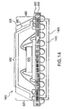
- FIG. 14 illustrates a cross-sectional view of a BGA package 1400 , in accordance with an embodiment of the present invention.
- mold compound 605 covers stiffener 620
- a peripheral dimension 1405 of stiffener 620 exceeds a peripheral dimension 1410 of cap body 625 .
- Peripheral dimension 1405 of stiffener 620 can exceed (as shown in FIG. 14 ), be equal to (as shown in FIGS. 17 and 18 , described below), or be less than (not shown) peripheral dimension 1410 of cap body 625 .
- FIG. 15 illustrates a cross-sectional view of a BGA package 1500 , in accordance with an embodiment of the present invention.
- cap body 625 is attached to stiffener 620 before encapsulating IC die 615 .
- Mold gate openings 1505 through sidewall portions 685 of cap body 625 facilitate injection of mold compound 605 into cavity 630 .
- FIG. 16 illustrates a cross-sectional view of a BGA package 1600 , in accordance with an embodiment of the present invention.
- a dam 1610 is applied to stiffener 620 and/or rim 665 around the periphery of cap body 625 .
- Mold compound 605 is deposited between dam 1610 and cap body 625 , and flows into cavity 630 through mold gate openings 1605 .
- first surface 690 of top portion 660 of cap body 625 is exposed through mold compound 605 (e.g., not covered).
- FIG. 17 illustrates a cross-sectional view of a BGA package 1700 , in accordance with an embodiment of the present invention.
- cap body 625 is attached to stiffener 620 after encapsulating IC die 615 (such as by a mold injection encapsulation process).
- an air gap 1720 exists between cap body 625 and mold compound 605 in cavity 630 .
- Pressure within cavity 630 due to air gap 1720 can build up at elevated temperatures during assembly, qualification, and testing of BGA package 1700 .
- a pressure release opening 1715 through sidewall portion 685 of cap body 625 allows gas, which is released from the materials within cavity 630 , to escape from air gap 1720 and balance cavity pressure with the ambient pressure.
- FIG. 18 illustrates a cross-sectional view of a BGA package 1800 , in accordance with an embodiment of the present invention.
- mold compound 605 is deposited within a dam 1810 , around IC die 615 , using a dam-and-fill encapsulation process.
- cap body 625 is attached to stiffener 620 .
- an air gap 1820 exists between cap body 625 and mold compound 605 in cavity 630 .
- a pressure release opening 1815 through sidewall portion 685 of cap body 625 allows gas, which is released from the materials within cavity 630 , to escape from air gap 1820 and balance cavity pressure with the ambient pressure.
- FIG. 19 illustrates a cross-sectional view of a BGA package 1900 , in accordance with an embodiment of the present invention.
- a pressure release opening 1915 is formed through top portion 660 of cap body 625 .
- a diameter of pressure release opening 1915 is selected to limit passage of EMI.
- the diameter of pressure release opening 1915 can be, for example, in the range of about 0.2 mm to about 2 mm (e.g., a diameter of about 0.5 mm can shield EMI having highest harmonic frequencies of up to 30 GHz), and can also be outside of this range, depending on the particular application.
- the diameter need not meet mold gate opening diameter requirements, described above, because cap structure 625 is attached to stiffener 620 after encapsulation. Therefore, mold compound 605 need not flow through pressure release opening 1915 into cavity 630 .
- FIGS. 20-24 illustrate cross-sectional views of BGA packages, in accordance with embodiments of the present invention, with additional thermal enhancements. These additional thermal enhancements can also be incorporated into the BGA packages described elsewhere herein, including those shown in FIGS. 12 , 17 - 19 , 25 , 26 , 28 and 29 .
- FIG. 20 illustrates a cross-sectional view of a BGA package 2000 , in accordance with an embodiment of the present invention.
- BGA package 2000 includes and IC die 2015 , a package substrate 2010 , a stiffener 2020 , a cap body 2025 , and a thermal/electrical connector 2040 .
- IC die 2015 is mounted to a central area of top surface 2001 of stiffener 2020 .
- a second surface 2002 of stiffener 2020 is attached to substrate 2010 .
- Substrate 2010 has a central opening 2070 that exposes a central area 2006 of second surface 2002 of stiffener 2020 .
- Cap body 2025 is attached to top surface 2001 of stiffener 2020 , forming a die enclosure 2080 .
- Thermal/electrical connector 2040 (also referred to herein as a “heat slug”) is attached to central area 2006 of second surface 2002 of stiffener 2020 through opening 2070 in substrate 2010 .
- Thermal/electrical connector 2040 is configured to be soldered to a PCB during surface mount.
- BGA package 2000 provides enhanced heat spreading because thermal/electrical connector 2040 reduces the thermal resistance between IC die 2015 and the PCB.
- connector 2040 can be attached to a ground or other potential of the PCB.
- BGA package 2000 also provides enhanced EMI shielding because thermal/electrical connector 2040 reduces the ground (or other voltage) connection impedance of die enclosure 2080 to the PCB.
- BGA package 2000 is encapsulated by dam-and-fill encapsulation. After cap body 2025 is attached to stiffener 2020 , a dam 2045 is applied around the periphery of cap body 2025 , partially covering stiffener 2020 . A mold compound 2005 is subsequently applied, filling the area between dam 2045 and cap body 2025 . Mold compound 2005 flows into a cavity 2030 through one or more mold gate openings 2050 in sidewall portions 2085 of cap body 2025 .
- FIG. 21 illustrates a cross-sectional view of a BGA package 2100 , in accordance with an embodiment of the present invention.
- BGA package 2100 is similar to BGA package 2000 , shown in FIG. 20 , except that the edges of stiffener 2020 are not flush with the edges of substrate 2010 . Instead, the edges of stiffener 2020 are flush with those of cap body 2025 .
- FIG. 22 illustrates a cross-sectional view of a BGA package 2200 , in accordance with an embodiment of the present invention.
- BGA package 2200 is similar to BGA package 2000 , shown in FIG. 20 , except that BGA package 2200 is encapsulated by a mold injection process.
- mold compound 2005 does not extend to the edges of stiffener 2020 , leaving areas 2201 of stiffener 2020 exposed through, or not covered by mold compound 2005 .
- FIG. 23 illustrates a cross-sectional view of a BGA package 2300 , in accordance with an embodiment of the present invention.
- BGA package 2300 is similar to BGA package 2200 , shown in FIG. 22 , except that mold compound 2005 extends to the edges of stiffener 2020 .
- BGA package 2300 can be encapsulated over the entire substrate strip or panel and separated by a saw singulation process.
- FIG. 24 illustrates a cross-sectional view of a BGA package 2400 , in accordance with an embodiment of the present invention.
- BGA package 2400 is similar to BGA package 1600 , shown in FIG. 16 , except that an external heat sink 2475 is attached to top portion 2460 of cap body 2425 with a thermally and/or electrically conductive interface or adhesive material 2470 .
- Cap body 2425 and a stiffener 2420 form a die enclosure 2480 .
- External heat sink 2475 enhances heat spreading; however, it can operate as an antenna that undesirably radiates EMI.
- a heat sink ground jumper wire can be used to ground the external heat sink to a PCB.
- a ground jumper wire is not required, however, if the external heat sink is attached to a grounded die enclosure.
- a heat sink ground jumper wire is not required for BGA package 2400 because external heat sink 2475 is attached to die enclosure 2480 , which is coupled to a ground potential through ground wires bonds 2430 and/or 2435 .
- a cap structure in a die-up array-type IC device package can have various configurations.
- Another example configuration is a one-piece cap structure having no rim, which is referred to herein as a “can” structure.
- An example of a can structure is described as follows with respect to FIG. 25 .
- FIG. 25A illustrates a cross-sectional view of a BGA package 2500 , in accordance with an embodiment of the present invention.
- BGA package 2500 includes an IC die 2515 , a printed circuit substrate 2510 , a stiffener 2520 , and a can body 2525 .
- IC die 2515 is mounted to a center region of a first surface 2521 of stiffener 2520 with a die attach material 2524 , such as epoxy or solder.
- Can body 2525 and stiffener 2520 form a die enclosure 2580 that substantially surrounds IC die 2515 .
- a second surface 2522 of stiffener 2520 is attached to a first surface 2511 of a package substrate 2510 .
- a plurality of solder balls 2513 is coupled to a second surface 2512 of substrate 2510 . Solder balls 2513 are reflowed to attach package 2500 to a PCB.
- BGA package 2500 further includes openings 2535 , wire bonds 2540 and 2550 , and a mold compound 2505 .
- Openings 2535 formed in stiffener 2520 facilitate interconnection of one or more wire bonds 2540 between corresponding bond pads 2545 and substrate 2510 .
- Pads 2545 can be any type of signal pads of IC die 2515 , such as I/O pads, voltage pads, ground pads, etc.
- One or more wire bonds 2550 couple ground pads 2546 to stiffener 2520 .
- Pads 2546 can be any type of signals pads of IC die 2515 , such as I/O pads, voltage pads, etc.
- Mold compound 2505 encapsulates IC die 2515 and wire bonds 2540 and 2550 .
- FIG. 25B illustrates a cross-sectional view of can body 2525 , shown in FIG. 25A .
- a can body 2525 has a horizontal planar top portion 2560 and sidewall portions 2585 that form a ninety degree angle to top portion 2560 .
- Can body 2525 further has a first surface 2590 and a second surface 2591 .
- Second surface 2591 has a cavity 2530 with a rectangular cross-section formed therein. Second surface 2591 is coupled to a first surface 2521 of stiffener 2520 .
- Die enclosure 2580 provides enhanced heat spreading and EMI shielding, while also providing enhanced structural integrity and environmental protection for package 2500 .
- BGA package 2500 is similar to BGA package 600 , described above. Accordingly, features of BGA package 600 described above are generally similar to the corresponding features of BGA package 2500 (e.g., example materials for the can structure, stiffener, substrate, encapsulating material, etc.; use of electrically conductive plated areas to enhance electrical coupling of the can structure to the stiffener; use of interlocking tabs and receptacles to enhance structural coupling of the can structure to the stiffener; use of a thermal/electrical connector and/or an external heart sink to enhance heat spreading; etc.).
- these features are not necessarily described in detail here for reasons of brevity.
- a cap structure is a two-piece cap structure.
- a two-piece cap structure may have a frame-shaped bottom portion, which is coupled to a stiffener, and a planar top portion, which is coupled to the frame-shaped portion.
- the frame-shaped bottom and planar top portions are referred to herein as “ring” and “lid” structures, respectively, and are described as follows with respect to FIGS. 26-29 .
- FIG. 26 illustrates a cross-sectional view of a BGA package 2600 , in accordance with an embodiment of the present invention.
- BGA package 2600 includes an IC die 2615 , a printed circuit substrate 2610 , a stiffener 2620 , a ring structure 2625 , and a lid structure 2626 .
- ring structure 2625 is a frame-shaped structure having a central opening.
- Lid structure 2626 is planar and has first and second surfaces 2661 and 2662 , respectively.
- a peripheral portion of second surface 2662 of lid structure 2626 is coupled to a first surface 2624 of ring structure 2625 .
- ring structure 2625 and lid structure 2626 form a cavity 2630 .
- Cavity 2630 has a rectangular cross-section.
- a second surface 2623 of ring structure 2625 is attached to a first surface 2621 of stiffener 2620 .
- IC die 2615 is mounted to a center region of first surface 2621 of stiffener 2620 with a die attach material 2675 , such as epoxy or solder.
- a die attach material 2675 such as epoxy or solder.
- Lid structure 2626 , ring structure 2625 , and stiffener 2620 form a die enclosure 2680 that substantially surrounds IC die 2615 .
- a second surface 2622 of stiffener 2620 is attached to a first surface 2611 of package substrate 2610 .
- a plurality of solder balls 2613 is coupled to a second surface 2612 of substrate 2610 . Solder balls 2613 are reflowed to attach package 2600 to a PCB.
- BGA package 2600 further includes openings 2635 , wire bonds 2640 and 2650 , and mold compound 2605 . Openings 2635 formed in stiffener 2620 facilitate interconnection of one or more wire bonds 2640 between corresponding bond pads 2645 and substrate 2610 . One or more wire bonds 2650 couple ground pads 2646 to stiffener 2620 . Pads 2645 and 2646 can be any type of signal pads of IC die 2615 , such as I/O pads, voltage pads, ground pads, etc. Mold compound 2605 encapsulates IC die 2615 and wire bonds 2640 and 2650 . Dam-and-fill encapsulation, or any other encapsulation techniques, can be used to encapsulate IC die 2615 before attaching lid 2626 .
- Mold compound 2605 can be filled to just below first surface 2624 of ring structure 2625 so that a gap 2670 is formed between second surface 2662 of lid structure 2626 and mold compound 2605 .
- die enclosure 2680 can be completely filled with mold compound 2605 , so that no gap remains.
- BGA package 2600 further includes a pressure release opening 2665 that extends through a sidewall portion of ring structure 2625 .
- FIG. 27 illustrates a perspective view of ring structure 2625 , which has a groove 2710 formed on first surface 2624 .
- groove 2710 forms pressure release opening 2665 .
- Gas which can be released from materials within cavity 2630 , can escape through pressure release opening 2665 and balance the cavity pressure with the ambient pressure.
- ring structure 2625 can have a pressure release opening formed through an edge portion (not shown).
- FIG. 28 illustrates a cross-sectional view of a BGA package 2800 , in accordance with an embodiment of the present invention, with ring and lid structures integrated with a stiffener.
- BGA package 2800 is similar to BGA package 2600 , shown in FIG. 26 , except that a peripheral dimension 2801 of lid structure 2626 is within a peripheral dimension 2802 of ring structure 2625 .
- lid structure 2626 can be “recess-mounted” to ring structure 2625 , as shown in FIG. 28 .
- lid structure 2626 resides in a recessed inner edge 2804 located around the top surface of ring structure 2625 .
- first surface 2661 of lid structure 2626 can be substantially planar with first surface 2624 of ring structure 2625 . Recess-mounting lid structure 2626 on ring structure 2625 , as shown in FIG. 28 , may enhance structural interlocking of lid structure 2626 and ring structure 2625 .
- FIG. 29 illustrates a cross-sectional view of a BGA package 2900 , in accordance with an embodiment of the present invention, with ring and lid structures integrated with a stiffener.
- BGA package 2900 is similar to BGA package 2800 , shown in FIG. 28 , except when lid structure 2626 is recess-mounted on ring structure 2625 , first surface 2661 of lid structure 2626 protrudes above first surface 2624 of ring structure 2625 .
- a recessed inner edge 2902 around the top of ring structure 2625 has a depth that is less than a thickness of lid structure 2626 .
- Recess-mounting lid structure 2626 on ring structure 2625 may enhance structural interlocking of lid structure 2626 and ring structure 2625 .
- Die enclosure 2680 shown in FIGS. 26 , 28 , and 29 , provides enhanced heat spreading and EMI shielding, while also providing enhanced structural integrity and environmental protection for packages 2600 , 2800 , and 2900 , respectively.
- BGA packages 2600 , 2800 , and 2900 are similar to BGA package 600 , described above.
- features of BGA package 600 described above are generally similar to the corresponding features of BGA packages 2600 , 2800 , and 2900 (e.g., example materials for ring and lid structures, stiffener, substrate, encapsulating material, etc.; use of electrically conductive plated areas to enhance electrical coupling of the ring structure to the stiffener; use of interlocking tabs and receptacles to enhance structural coupling of the ring structure to the stiffener; use of a thermal/electrical connector and/or an external heart sink to enhance heat spreading; etc.).
- these features are not necessarily described in detail here for reasons of brevity.
- FIG. 34 illustrates a cross-sectional view of a BGA package 3400 , in accordance with an embodiment of the present invention.
- BGA package 3400 includes an IC die 3415 , a printed circuit substrate 3410 , a stiffener 3420 , a ring structure 3425 , and a lid structure 3426 .
- FIG. 34 shows receptacles 3470 , 3474 , and 3478 formed in stiffener 3420 .
- Receptacles 3470 , 3474 , and 3478 are configured to be coupled with corresponding tabs 3472 , 3476 , and 3480 , respectively, patterned on ring structure 3425 .
- FIG. 34 also shows an external heat sink 3475 attached to lid 3426 .
- FIG. 30 shows a flowchart 3000 providing steps for assembling a die-up array IC device package with enhanced thermal and/or EMI shielding properties according to one or more embodiments of the present invention.
- FIGS. 31-33 provide additional optional steps, according to further embodiments of the present invention. The steps of FIGS. 30-33 do not necessarily have to occur in the order shown, as will be apparent to persons skilled in the relevant art(s) based on the teachings herein. Other operational and structural embodiments will be apparent to persons skilled in the relevant art(s) based on the following discussion. These steps are described in detail below.
- Flowchart 3000 is shown in FIG. 30 , and begins with step 3005 .
- an IC die is mounted to a first surface of a stiffener.
- the IC die is IC die 615 and the stiffener is stiffener 620 , as shown in FIG. 6A , or any one of the stiffeners shown in FIGS. 7A-7C , 9 A- 9 C, 10 - 12 , 14 - 26 , 28 , and 29 .
- a cap body is coupled to the first surface of the stiffener.
- the first surface of the stiffener and a cavity in a second surface of the cap body form an enclosure that substantially encloses the IC die.
- the cap body is cap body 625
- the stiffener is stiffener 620
- the cavity is cavity 630
- the IC die is IC die 615
- the die enclosure is die enclosure 680 , as shown in FIG. 6A , or any one of the corresponding elements shown in FIGS. 6B , 7 A-C, 8 A and 8 B, 9 A- 9 C, 10 - 26 , 28 , and 29 .
- a second surface of the stiffener is coupled to a first surface of a substrate.
- the stiffener is stiffener 620 and the substrate is substrate 610 , shown in FIG. 6A , or any of the substrates shown in FIGS. 10-12 , 14 - 26 , 28 , and 29 .
- step 3010 of flowchart 3000 includes the additional steps shown in FIG. 31 .
- a second surface of a frame body is coupled to the first surface of the stiffener.
- the frame body is ring structure 2625
- the stiffener is stiffener 2610 , as shown in FIG. 26 , or any of the ring structures shown in FIGS. 27-29 .
- a second surface of a lid body is coupled to a first surface of the frame body.
- the stiffener, the frame body, and the lid body form an enclosure that substantially encloses the IC die.
- the lid body is lid structure 2626
- the frame body is ring structure 2625
- the stiffener is stiffener 2620
- the die enclosure is die enclosure 2680
- the IC die is IC die 2615 , as shown in FIG. 26 , or any of the corresponding elements shown in FIGS. 28 and 29 .
- flowchart 3000 includes one or more of the additional steps shown in FIG. 32 .
- steps 3205 , 3210 , and 3215 can be performed.
- step 3205 at least one mold gate opening is formed through a portion of the cap body.
- the cap body is cap body 625
- the at least one mold gate opening is mold gate opening 1105 , as shown in FIG. 11 , or any of the mold gate openings shown in FIGS. 12 , 13 , 15 , 16 , 20 , 21 , and 24 .
- step 3210 at least one pressure release opening is formed through a portion of the cap body.
- the cap body is cap body 625
- the at least one pressure release opening is pressure release opening 1715 , as shown in FIG. 17 , or any of the pressure release openings shown in FIGS. 18 and 19 .
- step 3215 the IC die is encapsulated with an encapsulating material.
- the IC die is IC die 615
- the encapsulating material is mold compound 605 , as shown in FIG. 6A , or any one of the corresponding elements shown in FIGS. 10-12 , 14 - 26 , 28 , and 29 .
- conventional IC die encapsulation processes can be used, such as dam-and-fill (glob top), injection molding, strip or panel over-molding, saw-singulation, and any other IC die encapsulation processes.
- flowchart 3000 includes one or more of the additional steps pertaining to thermal enhancement shown in FIG. 33 .
- steps 3305 and 3310 need not be performed in conjunction with step 3315
- step 3315 need not be performed in conjunction with steps 3305 and 3310 .
- a central opening is formed through the substrate.
- the substrate is substrate 2010
- the central opening is opening 2070 , as shown in FIG. 20 , or any of the corresponding elements shown in FIGS. 21-23 .
- a heat slug (also referred to herein as a “thermal/electrical connector”) is coupled to a portion of the second surface of the stiffener that is exposed through the central opening through the substrate.
- the heat slug is thermal/electrical connector 2040
- the stiffener is stiffener 2020
- the exposed second surface of the stiffener is exposed central area 2006
- the substrate is substrate 2010
- the central opening through the substrate is opening 2070 , as shown in FIG. 20 , or any of the corresponding elements shown in FIGS. 21-23 .
- an external heat sink is coupled to a portion of the cap body.
- the external heat sink is external heat sink 2475
- the cap body is cap body 2425
- the portion of the cap body to which the external heat sink is attached is top portion 2460 , as shown in FIG. 24 .
Landscapes
- Cooling Or The Like Of Semiconductors Or Solid State Devices (AREA)
- Shielding Devices Or Components To Electric Or Magnetic Fields (AREA)
- Structures Or Materials For Encapsulating Or Coating Semiconductor Devices Or Solid State Devices (AREA)
Abstract
Description
Claims (7)
Priority Applications (1)
| Application Number | Priority Date | Filing Date | Title |
|---|---|---|---|
| US12/352,309 US7791189B2 (en) | 2004-06-21 | 2009-01-12 | Multipiece apparatus for thermal and electromagnetic interference (EMI) shielding enhancement in die-up array packages and method of making the same |
Applications Claiming Priority (2)
| Application Number | Priority Date | Filing Date | Title |
|---|---|---|---|
| US10/870,929 US7482686B2 (en) | 2004-06-21 | 2004-06-21 | Multipiece apparatus for thermal and electromagnetic interference (EMI) shielding enhancement in die-up array packages and method of making the same |
| US12/352,309 US7791189B2 (en) | 2004-06-21 | 2009-01-12 | Multipiece apparatus for thermal and electromagnetic interference (EMI) shielding enhancement in die-up array packages and method of making the same |
Related Parent Applications (1)
| Application Number | Title | Priority Date | Filing Date |
|---|---|---|---|
| US10/870,929 Division US7482686B2 (en) | 2004-06-21 | 2004-06-21 | Multipiece apparatus for thermal and electromagnetic interference (EMI) shielding enhancement in die-up array packages and method of making the same |
Publications (2)
| Publication Number | Publication Date |
|---|---|
| US20090115048A1 US20090115048A1 (en) | 2009-05-07 |
| US7791189B2 true US7791189B2 (en) | 2010-09-07 |
Family
ID=35479790
Family Applications (2)
| Application Number | Title | Priority Date | Filing Date |
|---|---|---|---|
| US10/870,929 Expired - Lifetime US7482686B2 (en) | 2004-06-21 | 2004-06-21 | Multipiece apparatus for thermal and electromagnetic interference (EMI) shielding enhancement in die-up array packages and method of making the same |
| US12/352,309 Expired - Fee Related US7791189B2 (en) | 2004-06-21 | 2009-01-12 | Multipiece apparatus for thermal and electromagnetic interference (EMI) shielding enhancement in die-up array packages and method of making the same |
Family Applications Before (1)
| Application Number | Title | Priority Date | Filing Date |
|---|---|---|---|
| US10/870,929 Expired - Lifetime US7482686B2 (en) | 2004-06-21 | 2004-06-21 | Multipiece apparatus for thermal and electromagnetic interference (EMI) shielding enhancement in die-up array packages and method of making the same |
Country Status (1)
| Country | Link |
|---|---|
| US (2) | US7482686B2 (en) |
Cited By (8)
| Publication number | Priority date | Publication date | Assignee | Title |
|---|---|---|---|---|
| US20070267740A1 (en) * | 2006-05-16 | 2007-11-22 | Broadcom Corporation | Method and apparatus for cooling semiconductor device hot blocks and large scale integrated circuit (IC) using integrated interposer for IC packages |
| US20070290322A1 (en) * | 2006-06-20 | 2007-12-20 | Broadcom Corporation | Thermal improvement for hotspots on dies in integrated circuit packages |
| US20110156235A1 (en) * | 2009-12-29 | 2011-06-30 | Taiwan Semiconductor Manufacturing Company, Ltd. | Flip chip package having enhanced thermal and mechanical performance |
| US20120182694A1 (en) * | 2011-01-14 | 2012-07-19 | Taiwan Semiconductor Manufacturing Company, Ltd. | Lid Design for Reliability Enhancement in Flip Chip Package |
| US20140070397A1 (en) * | 2012-09-13 | 2014-03-13 | Lakshminarayan Viswanathan | High power semiconductor package subsystems |
| US9048597B2 (en) | 2012-10-19 | 2015-06-02 | Apple Inc. | Structures for securing printed circuit connectors |
| US11315883B2 (en) | 2019-11-12 | 2022-04-26 | Advanced Micro Devices, Inc. | Integrated circuit product customizations for identification code visibility |
| US11462476B2 (en) * | 2018-01-31 | 2022-10-04 | Tdk Electronics Ag | Electronic device |
Families Citing this family (94)
| Publication number | Priority date | Publication date | Assignee | Title |
|---|---|---|---|---|
| US7550845B2 (en) | 2002-02-01 | 2009-06-23 | Broadcom Corporation | Ball grid array package with separated stiffener layer |
| US7482686B2 (en) | 2004-06-21 | 2009-01-27 | Braodcom Corporation | Multipiece apparatus for thermal and electromagnetic interference (EMI) shielding enhancement in die-up array packages and method of making the same |
| US7432586B2 (en) * | 2004-06-21 | 2008-10-07 | Broadcom Corporation | Apparatus and method for thermal and electromagnetic interference (EMI) shielding enhancement in die-up array packages |
| US7786591B2 (en) * | 2004-09-29 | 2010-08-31 | Broadcom Corporation | Die down ball grid array package |
| DE102004049663B3 (en) * | 2004-10-11 | 2006-04-13 | Infineon Technologies Ag | Plastic housing and semiconductor device with such plastic housing and method for producing the same |
| US7271479B2 (en) * | 2004-11-03 | 2007-09-18 | Broadcom Corporation | Flip chip package including a non-planar heat spreader and method of making the same |
| US7629674B1 (en) | 2004-11-17 | 2009-12-08 | Amkor Technology, Inc. | Shielded package having shield fence |
| TWI263256B (en) * | 2005-05-03 | 2006-10-01 | Siliconware Precision Industries Co Ltd | Flip-chip semiconductor device |
| JP4492432B2 (en) * | 2005-05-13 | 2010-06-30 | 株式会社デンソー | Manufacturing method of physical quantity sensor device |
| US20070108583A1 (en) * | 2005-08-08 | 2007-05-17 | Stats Chippac Ltd. | Integrated circuit package-on-package stacking system |
| US8643163B2 (en) * | 2005-08-08 | 2014-02-04 | Stats Chippac Ltd. | Integrated circuit package-on-package stacking system and method of manufacture thereof |
| US7566591B2 (en) * | 2005-08-22 | 2009-07-28 | Broadcom Corporation | Method and system for secure heat sink attachment on semiconductor devices with macroscopic uneven surface features |
| US7582951B2 (en) | 2005-10-20 | 2009-09-01 | Broadcom Corporation | Methods and apparatus for improved thermal performance and electromagnetic interference (EMI) shielding in leadframe integrated circuit (IC) packages |
| US7342303B1 (en) | 2006-02-28 | 2008-03-11 | Amkor Technology, Inc. | Semiconductor device having RF shielding and method therefor |
| US20070200210A1 (en) * | 2006-02-28 | 2007-08-30 | Broadcom Corporation | Methods and apparatus for improved thermal performance and electromagnetic interference (EMI) shielding in integrated circuit (IC) packages |
| US7714453B2 (en) | 2006-05-12 | 2010-05-11 | Broadcom Corporation | Interconnect structure and formation for package stacking of molded plastic area array package |
| US8183680B2 (en) * | 2006-05-16 | 2012-05-22 | Broadcom Corporation | No-lead IC packages having integrated heat spreader for electromagnetic interference (EMI) shielding and thermal enhancement |
| US20070273023A1 (en) * | 2006-05-26 | 2007-11-29 | Broadcom Corporation | Integrated circuit package having exposed thermally conducting body |
| US7808087B2 (en) * | 2006-06-01 | 2010-10-05 | Broadcom Corporation | Leadframe IC packages having top and bottom integrated heat spreaders |
| TW200810040A (en) * | 2006-06-09 | 2008-02-16 | Nec Electronics Corp | Semiconductor device and apparatus and method for manufacturing the same |
| US8581381B2 (en) | 2006-06-20 | 2013-11-12 | Broadcom Corporation | Integrated circuit (IC) package stacking and IC packages formed by same |
| US20080054496A1 (en) | 2006-08-30 | 2008-03-06 | Neill Thornton | High temperature operating package and circuit design |
| US20080099910A1 (en) * | 2006-08-31 | 2008-05-01 | Ati Technologies Inc. | Flip-Chip Semiconductor Package with Encapsulant Retaining Structure and Strip |
| US20080054490A1 (en) | 2006-08-31 | 2008-03-06 | Ati Technologies Inc. | Flip-Chip Ball Grid Array Strip and Package |
| US7906844B2 (en) * | 2006-09-26 | 2011-03-15 | Compass Technology Co. Ltd. | Multiple integrated circuit die package with thermal performance |
| US8169067B2 (en) * | 2006-10-20 | 2012-05-01 | Broadcom Corporation | Low profile ball grid array (BGA) package with exposed die and method of making same |
| US20080197468A1 (en) * | 2007-02-15 | 2008-08-21 | Advanced Semiconductor Engineering, Inc. | Package structure and manufacturing method thereof |
| US8183687B2 (en) * | 2007-02-16 | 2012-05-22 | Broadcom Corporation | Interposer for die stacking in semiconductor packages and the method of making the same |
| US9466545B1 (en) * | 2007-02-21 | 2016-10-11 | Amkor Technology, Inc. | Semiconductor package in package |
| US7898066B1 (en) | 2007-05-25 | 2011-03-01 | Amkor Technology, Inc. | Semiconductor device having EMI shielding and method therefor |
| US7872335B2 (en) * | 2007-06-08 | 2011-01-18 | Broadcom Corporation | Lead frame-BGA package with enhanced thermal performance and I/O counts |
| US7745910B1 (en) | 2007-07-10 | 2010-06-29 | Amkor Technology, Inc. | Semiconductor device having RF shielding and method therefor |
| US7923846B2 (en) * | 2007-11-16 | 2011-04-12 | Stats Chippac Ltd. | Integrated circuit package-in-package system with wire-in-film encapsulant |
| US8178956B2 (en) * | 2007-12-13 | 2012-05-15 | Stats Chippac Ltd. | Integrated circuit package system for shielding electromagnetic interference |
| US8008753B1 (en) | 2008-04-22 | 2011-08-30 | Amkor Technology, Inc. | System and method to reduce shorting of radio frequency (RF) shielding |
| US7915715B2 (en) * | 2008-11-25 | 2011-03-29 | Amkor Technology, Inc. | System and method to provide RF shielding for a MEMS microphone package |
| US8129824B1 (en) | 2008-12-03 | 2012-03-06 | Amkor Technology, Inc. | Shielding for a semiconductor package |
| US8102032B1 (en) | 2008-12-09 | 2012-01-24 | Amkor Technology, Inc. | System and method for compartmental shielding of stacked packages |
| US8012868B1 (en) | 2008-12-15 | 2011-09-06 | Amkor Technology Inc | Semiconductor device having EMI shielding and method therefor |
| US7851894B1 (en) | 2008-12-23 | 2010-12-14 | Amkor Technology, Inc. | System and method for shielding of package on package (PoP) assemblies |
| JP5289996B2 (en) * | 2009-02-16 | 2013-09-11 | 日本特殊陶業株式会社 | Reinforced wiring board |
| US7960818B1 (en) | 2009-03-04 | 2011-06-14 | Amkor Technology, Inc. | Conformal shield on punch QFN semiconductor package |
| JP5843757B2 (en) * | 2009-05-19 | 2016-01-13 | ボーグワーナー インコーポレーテッド | Turbocharger |
| US8093691B1 (en) | 2009-07-14 | 2012-01-10 | Amkor Technology, Inc. | System and method for RF shielding of a semiconductor package |
| US8013438B2 (en) * | 2009-07-21 | 2011-09-06 | Stmicroelectronics Asia Pacific Pte. Ltd. | Semiconductor package with a stiffening member supporting a thermal heat spreader |
| US8362598B2 (en) * | 2009-08-26 | 2013-01-29 | Amkor Technology Inc | Semiconductor device with electromagnetic interference shielding |
| US8724339B2 (en) * | 2009-12-01 | 2014-05-13 | Apple Inc. | Compact media player |
| US8093714B2 (en) * | 2009-12-10 | 2012-01-10 | Semtech Corporation | Chip assembly with chip-scale packaging |
| US8199518B1 (en) | 2010-02-18 | 2012-06-12 | Amkor Technology, Inc. | Top feature package and method |
| US8946886B1 (en) | 2010-05-13 | 2015-02-03 | Amkor Technology, Inc. | Shielded electronic component package and method |
| US8508023B1 (en) | 2010-06-17 | 2013-08-13 | Amkor Technology, Inc. | System and method for lowering contact resistance of the radio frequency (RF) shield to ground |
| JP5633210B2 (en) | 2010-06-28 | 2014-12-03 | 富士通セミコンダクター株式会社 | Semiconductor device |
| TWI442523B (en) * | 2010-09-03 | 2014-06-21 | 日月光半導體製造股份有限公司 | Semiconductor structure with metal frame |
| FR2977975A1 (en) * | 2011-07-13 | 2013-01-18 | St Microelectronics Grenoble 2 | THERMAL VIA ELECTRONIC HOUSING AND METHOD OF MANUFACTURE |
| KR101801945B1 (en) * | 2011-08-09 | 2017-11-28 | 에스케이하이닉스 주식회사 | Semiconductor chip and semiconductor package having the same |
| KR101274460B1 (en) * | 2011-11-22 | 2013-06-18 | 삼성전기주식회사 | Semiconductor package and manufacturing method threrof |
| US8986806B1 (en) | 2012-04-20 | 2015-03-24 | Amkor Technology, Inc. | Warpage control stiffener ring package and fabrication method |
| TW201349410A (en) * | 2012-05-31 | 2013-12-01 | 鴻海精密工業股份有限公司 | Chip package structure and method |
| ITVI20130077A1 (en) | 2013-03-20 | 2014-09-21 | St Microelectronics Srl | A GRAPHENE-BASED FILLER MATERIAL WITH A HIGH THERMAL CONDUCTIVITY FOR THE CONNECTION OF CHIPS IN MICRO-STRUCTURE DEVICES |
| TWI503944B (en) * | 2013-04-18 | 2015-10-11 | 矽品精密工業股份有限公司 | Shield, semiconductor package and manufacturing method thereof and package structure having the same |
| JP2014229761A (en) * | 2013-05-23 | 2014-12-08 | 株式会社東芝 | Electronic apparatus |
| US9713851B2 (en) * | 2013-09-04 | 2017-07-25 | Apple Inc. | Method and system for attaching flexible circuits to a mounting surface |
| US9064838B2 (en) * | 2013-09-17 | 2015-06-23 | Freescale Semiconductor, Inc. | Heat spreader for integrated circuit device |
| US9832860B2 (en) * | 2014-09-26 | 2017-11-28 | Intel Corporation | Panel level fabrication of package substrates with integrated stiffeners |
| US9502368B2 (en) | 2014-12-16 | 2016-11-22 | Intel Corporation | Picture frame stiffeners for microelectronic packages |
| US10410948B2 (en) * | 2015-01-30 | 2019-09-10 | Netgear, Inc. | Integrated heat sink and electromagnetic interference (EMI) shield assembly |
| KR102468259B1 (en) * | 2015-03-06 | 2022-11-18 | 삼성전자주식회사 | Circuit element package, manufacturing method thereof, and manufacturing apparatus thereof |
| WO2016144039A1 (en) * | 2015-03-06 | 2016-09-15 | Samsung Electronics Co., Ltd. | Circuit element package, manufacturing method thereof, and manufacturing apparatus thereof |
| DE102015108700B4 (en) | 2015-06-02 | 2025-01-09 | Infineon Technologies Austria Ag | Semiconductor power package and method for its manufacture |
| US9847304B2 (en) * | 2015-12-24 | 2017-12-19 | Intel Corporation | Electronic device packages with conformal EMI shielding and related methods |
| US10477737B2 (en) | 2016-05-04 | 2019-11-12 | Samsung Electronics Co., Ltd. | Manufacturing method of a hollow shielding structure for circuit elements |
| US20170330827A1 (en) * | 2016-05-12 | 2017-11-16 | Digi International Inc. | Hybrid embedded surface mount module form factor with same signal source subset mapping |
| US10477687B2 (en) | 2016-08-04 | 2019-11-12 | Samsung Electronics Co., Ltd. | Manufacturing method for EMI shielding structure |
| CN106340506A (en) * | 2016-10-20 | 2017-01-18 | 江苏长电科技股份有限公司 | Semiconductor packaging structure and manufacturing method thereof |
| KR102551657B1 (en) | 2016-12-12 | 2023-07-06 | 삼성전자주식회사 | EMI shielding structure and manufacturing method for the same |
| IT201700000485A1 (en) * | 2017-01-03 | 2018-07-03 | St Microelectronics Srl | CORRESPONDING EQUIPMENT, SEMICONDUCTOR AND EQUIPMENT |
| US10177095B2 (en) | 2017-03-24 | 2019-01-08 | Amkor Technology, Inc. | Semiconductor device and method of manufacturing thereof |
| JP2018170419A (en) * | 2017-03-30 | 2018-11-01 | 太陽誘電株式会社 | Electronic component module |
| JP6689780B2 (en) | 2017-03-30 | 2020-04-28 | 太陽誘電株式会社 | Method for manufacturing electronic component module |
| US10497650B2 (en) | 2017-04-13 | 2019-12-03 | Amkor Technology, Inc. | Semiconductor device and manufacturing method thereof |
| US11101224B2 (en) * | 2017-06-08 | 2021-08-24 | Futurewei Technologies, Inc. | Wrapped signal shielding in a wafer fanout package |
| CN107331787B (en) * | 2017-06-26 | 2019-06-21 | 京东方科技集团股份有限公司 | Encapsulation cover plate, organic light emitting display and preparation method thereof |
| US10594020B2 (en) | 2017-07-19 | 2020-03-17 | Samsung Electronics Co., Ltd. | Electronic device having antenna element and method for manufacturing the same |
| US10679929B2 (en) * | 2017-07-28 | 2020-06-09 | Advanced Semiconductor Engineering Korea, Inc. | Semiconductor package device and method of manufacturing the same |
| KR102373931B1 (en) | 2017-09-08 | 2022-03-14 | 삼성전자주식회사 | Electromagnetic interference shielding structure |
| US10651127B2 (en) | 2017-09-29 | 2020-05-12 | Intel Corporation | Ring-in-ring configurable-capacitance stiffeners and methods of assembling same |
| US10764996B1 (en) * | 2018-06-19 | 2020-09-01 | Xilinx, Inc. | Chip package assembly with composite stiffener |
| US11038267B2 (en) * | 2018-07-31 | 2021-06-15 | Skyworks Solutions, Inc. | Apparatus and methods for electromagnetic shielding using an outer cobalt layer |
| US10770369B2 (en) * | 2018-08-24 | 2020-09-08 | Advanced Semiconductor Engineering, Inc. | Semiconductor device package |
| US11935799B2 (en) * | 2019-06-25 | 2024-03-19 | Intel Corporation | Integrated circuit package lids with polymer features |
| US11367628B2 (en) * | 2019-07-16 | 2022-06-21 | Advanced Micro Devices, Inc. | Molded chip package with anchor structures |
| US12543572B2 (en) * | 2022-03-09 | 2026-02-03 | Micron Technology, Inc. | Semiconductor systems with anti-warpage mechanisms and associated systems, devices, and methods |
| US20230420384A1 (en) * | 2022-06-24 | 2023-12-28 | Intel Corporation | Slotted stiffener for a package substrate |
| US12519067B2 (en) * | 2022-08-25 | 2026-01-06 | Taiwan Semiconductor Manufacturing Company Limited | Two-piece type stiffener structure with beveled surface for delamination reduction and methods for forming the same |
Citations (170)
| Publication number | Priority date | Publication date | Assignee | Title |
|---|---|---|---|---|
| US3790866A (en) | 1973-05-14 | 1974-02-05 | Gen Motors Corp | Semiconductor device enclosure and method of making same |
| US4611238A (en) | 1982-05-05 | 1986-09-09 | Burroughs Corporation | Integrated circuit package incorporating low-stress omnidirectional heat sink |
| US5045921A (en) | 1989-12-26 | 1991-09-03 | Motorola, Inc. | Pad array carrier IC device using flexible tape |
| US5065281A (en) | 1990-02-12 | 1991-11-12 | Rogers Corporation | Molded integrated circuit package incorporating heat sink |
| US5153379A (en) | 1990-10-09 | 1992-10-06 | Motorola, Inc. | Shielded low-profile electronic component assembly |
| DE4213251A1 (en) | 1991-04-23 | 1992-10-29 | Mitsubishi Electric Corp | Semiconductor chip with insulating frame - including heat sink and conductive structure |
| US5173766A (en) | 1990-06-25 | 1992-12-22 | Lsi Logic Corporation | Semiconductor device package and method of making such a package |
| US5208504A (en) | 1990-12-28 | 1993-05-04 | Raytheon Company | Saw device and method of manufacture |
| US5216278A (en) | 1990-12-04 | 1993-06-01 | Motorola, Inc. | Semiconductor device having a pad array carrier package |
| EP0573297A2 (en) | 1992-06-04 | 1993-12-08 | Shinko Electric Industries Co. Ltd. | Semiconductor device comprising a TAB tape |
| US5285352A (en) | 1992-07-15 | 1994-02-08 | Motorola, Inc. | Pad array semiconductor device with thermal conductor and process for making the same |
| US5291062A (en) | 1993-03-01 | 1994-03-01 | Motorola, Inc. | Area array semiconductor device having a lid with functional contacts |
| US5294826A (en) | 1993-04-16 | 1994-03-15 | Northern Telecom Limited | Integrated circuit package and assembly thereof for thermal and EMI management |
| US5366589A (en) | 1993-11-16 | 1994-11-22 | Motorola, Inc. | Bonding pad with circular exposed area and method thereof |
| US5394009A (en) | 1993-07-30 | 1995-02-28 | Sun Microsystems, Inc. | Tab semiconductor package with cushioned land grid array outer lead bumps |
| US5397917A (en) | 1993-04-26 | 1995-03-14 | Motorola, Inc. | Semiconductor package capable of spreading heat |
| US5397921A (en) | 1993-09-03 | 1995-03-14 | Advanced Semiconductor Assembly Technology | Tab grid array |
| US5433631A (en) | 1993-01-26 | 1995-07-18 | International Business Machines Corporation | Flex circuit card elastomeric cable connector assembly |
| US5438216A (en) | 1992-08-31 | 1995-08-01 | Motorola, Inc. | Light erasable multichip module |
| US5474957A (en) | 1994-05-09 | 1995-12-12 | Nec Corporation | Process of mounting tape automated bonded semiconductor chip on printed circuit board through bumps |
| US5490324A (en) | 1993-09-15 | 1996-02-13 | Lsi Logic Corporation | Method of making integrated circuit package having multiple bonding tiers |
| US5534467A (en) | 1993-03-18 | 1996-07-09 | Lsi Logic Corporation | Semiconductor packages for high I/O semiconductor dies |
| US5541450A (en) | 1994-11-02 | 1996-07-30 | Motorola, Inc. | Low-profile ball-grid array semiconductor package |
| US5552635A (en) | 1994-01-11 | 1996-09-03 | Samsung Electronics Co., Ltd. | High thermal emissive semiconductor device package |
| US5572405A (en) | 1995-06-07 | 1996-11-05 | International Business Machines Corporation (Ibm) | Thermally enhanced ball grid array package |
| US5578869A (en) | 1994-03-29 | 1996-11-26 | Olin Corporation | Components for housing an integrated circuit device |
| US5583378A (en) | 1994-05-16 | 1996-12-10 | Amkor Electronics, Inc. | Ball grid array integrated circuit package with thermal conductor |
| US5583377A (en) | 1992-07-15 | 1996-12-10 | Motorola, Inc. | Pad array semiconductor device having a heat sink with die receiving cavity |
| US5642261A (en) | 1993-12-20 | 1997-06-24 | Sgs-Thomson Microelectronics, Inc. | Ball-grid-array integrated circuit package with solder-connected thermal conductor |
| US5648679A (en) | 1994-09-16 | 1997-07-15 | National Semiconductor Corporation | Tape ball lead integrated circuit package |
| US5650659A (en) | 1995-08-04 | 1997-07-22 | National Semiconductor Corporation | Semiconductor component package assembly including an integral RF/EMI shield |
| US5650662A (en) | 1993-08-17 | 1997-07-22 | Edwards; Steven F. | Direct bonded heat spreader |
| US5668406A (en) | 1994-05-31 | 1997-09-16 | Nec Corporation | Semiconductor device having shielding structure made of electrically conductive paste |
| US5691567A (en) | 1995-09-19 | 1997-11-25 | National Semiconductor Corporation | Structure for attaching a lead frame to a heat spreader/heat slug structure |
| US5717252A (en) | 1994-07-25 | 1998-02-10 | Mitsui High-Tec, Inc. | Solder-ball connected semiconductor device with a recessed chip mounting area |
| US5732465A (en) | 1994-07-15 | 1998-03-31 | Shinko Electric Industries Co., Ltd. | Method of manufacturing one side resin sealing type semiconductor devices |
| US5736785A (en) | 1996-12-20 | 1998-04-07 | Industrial Technology Research Institute | Semiconductor package for improving the capability of spreading heat |
| US5744863A (en) | 1994-07-11 | 1998-04-28 | International Business Machines Corporation | Chip carrier modules with heat sinks attached by flexible-epoxy |
| EP0504411B1 (en) | 1990-09-19 | 1998-06-17 | Fujitsu Limited | Semiconductor device having many lead pins |
| US5796170A (en) | 1996-02-15 | 1998-08-18 | Northern Telecom Limited | Ball grid array (BGA) integrated circuit packages |
| US5798909A (en) | 1995-02-15 | 1998-08-25 | International Business Machines Corporation | Single-tiered organic chip carriers for wire bond-type chips |
| US5801432A (en) | 1992-06-04 | 1998-09-01 | Lsi Logic Corporation | Electronic system using multi-layer tab tape semiconductor device having distinct signal, power and ground planes |
| US5835355A (en) | 1997-09-22 | 1998-11-10 | Lsi Logic Corporation | Tape ball grid array package with perforated metal stiffener |
| US5843808A (en) | 1996-01-11 | 1998-12-01 | Asat, Limited | Structure and method for automated assembly of a tab grid array package |
| US5844168A (en) | 1995-08-01 | 1998-12-01 | Minnesota Mining And Manufacturing Company | Multi-layer interconnect sutructure for ball grid arrays |
| US5856911A (en) | 1996-11-12 | 1999-01-05 | National Semiconductor Corporation | Attachment assembly for integrated circuits |
| US5866949A (en) | 1996-12-02 | 1999-02-02 | Minnesota Mining And Manufacturing Company | Chip scale ball grid array for integrated circuit packaging |
| US5883430A (en) | 1996-06-19 | 1999-03-16 | International Business Machines Corporation | Thermally enhanced flip chip package |
| US5889324A (en) | 1998-03-30 | 1999-03-30 | Nec Corporation | Package for a semiconductor device |
| US5889321A (en) | 1997-06-17 | 1999-03-30 | International Business Machines Corporation | Stiffeners with improved adhesion to flexible substrates |
| US5894410A (en) | 1996-03-28 | 1999-04-13 | Intel Corporation | Perimeter matrix ball grid array circuit package with a populated center |
| US5895967A (en) | 1997-07-07 | 1999-04-20 | Texas Instruments Incorporated | Ball grid array package having a deformable metal layer and method |
| US5901041A (en) | 1997-12-02 | 1999-05-04 | Northern Telecom Limited | Flexible integrated circuit package |
| US5903052A (en) | 1998-05-12 | 1999-05-11 | Industrial Technology Research Institute | Structure for semiconductor package for improving the efficiency of spreading heat |
| US5905633A (en) | 1996-02-29 | 1999-05-18 | Anam Semiconductor Inc. | Ball grid array semiconductor package using a metal carrier ring as a heat spreader |
| US5907189A (en) | 1997-05-29 | 1999-05-25 | Lsi Logic Corporation | Conformal diamond coating for thermal improvement of electronic packages |
| US5907903A (en) | 1996-05-24 | 1999-06-01 | International Business Machines Corporation | Multi-layer-multi-chip pyramid and circuit board structure and method of forming same |
| US5920117A (en) | 1994-08-02 | 1999-07-06 | Fujitsu Limited | Semiconductor device and method of forming the device |
| US5949137A (en) | 1997-09-26 | 1999-09-07 | Lsi Logic Corporation | Stiffener ring and heat spreader for use with flip chip packaging assemblies |
| US5953589A (en) | 1996-12-30 | 1999-09-14 | Anam Semiconductor Inc. | Ball grid array semiconductor package with solder balls fused on printed circuit board and method for fabricating the same |
| US5972734A (en) | 1997-09-17 | 1999-10-26 | Lsi Logic Corporation | Interposer for ball grid array (BGA) package |
| US5977626A (en) | 1998-08-12 | 1999-11-02 | Industrial Technology Research Institute | Thermally and electrically enhanced PBGA package |
| US5977633A (en) | 1996-08-15 | 1999-11-02 | Nec Corporation | Semiconductor device with metal base substrate having hollows |
| US5976912A (en) | 1994-03-18 | 1999-11-02 | Hitachi Chemical Company, Ltd. | Fabrication process of semiconductor package and semiconductor package |
| US5982621A (en) | 1998-11-23 | 1999-11-09 | Caesar Technology Inc. | Electronic device cooling arrangement |
| US5986340A (en) | 1996-05-02 | 1999-11-16 | National Semiconductor Corporation | Ball grid array package with enhanced thermal and electrical characteristics and electronic device incorporating same |
| US5986885A (en) | 1997-04-08 | 1999-11-16 | Integrated Device Technology, Inc. | Semiconductor package with internal heatsink and assembly method |
| US5998241A (en) | 1997-12-08 | 1999-12-07 | Nec Corporation | Semiconductor device and method of manufacturing the same |
| US5999415A (en) | 1998-11-18 | 1999-12-07 | Vlsi Technology, Inc. | BGA package using PCB and tape in a die-down configuration |
| US6002147A (en) | 1996-09-26 | 1999-12-14 | Samsung Electronics Company | Hybrid microwave-frequency integrated circuit |
| US6002169A (en) | 1998-06-15 | 1999-12-14 | Lsi Logic Corporation | Thermally enhanced tape ball grid array package |
| US6011304A (en) | 1997-05-05 | 2000-01-04 | Lsi Logic Corporation | Stiffener ring attachment with holes and removable snap-in heat sink or heat spreader/lid |
| US6011694A (en) | 1996-08-01 | 2000-01-04 | Fuji Machinery Mfg. & Electronics Co., Ltd. | Ball grid array semiconductor package with solder ball openings in an insulative base |
| US6020637A (en) | 1997-05-07 | 2000-02-01 | Signetics Kp Co., Ltd. | Ball grid array semiconductor package |
| US6028358A (en) | 1996-05-30 | 2000-02-22 | Nec Corporation | Package for a semiconductor device and a semiconductor device |
| TW383908U (en) | 1998-09-22 | 2000-03-01 | Caesar Technology Inc | Structure used for increasing heat-dissipation of micro-electronic apparatus |
| US6034427A (en) | 1998-01-28 | 2000-03-07 | Prolinx Labs Corporation | Ball grid array structure and method for packaging an integrated circuit chip |
| US6040984A (en) | 1996-02-27 | 2000-03-21 | Fuji Machinery Mfg. & Electronics Co., Ltd. | Printed circuit board with opposed bonding shelves for semiconductor chip wire bonding at different levels |
| US6057601A (en) | 1998-11-27 | 2000-05-02 | Express Packaging Systems, Inc. | Heat spreader with a placement recess and bottom saw-teeth for connection to ground planes on a thin two-sided single-core BGA substrate |
| US6060777A (en) | 1998-07-21 | 2000-05-09 | Intel Corporation | Underside heat slug for ball grid array packages |
| US6064111A (en) | 1996-07-31 | 2000-05-16 | Hitachi Company, Ltd. | Substrate for holding a chip of semi-conductor package, semi-conductor package, and fabrication process of semi-conductor package |
| US6069407A (en) | 1998-11-18 | 2000-05-30 | Vlsi Technology, Inc. | BGA package using PCB and tape in a die-up configuration |
| US6077724A (en) | 1998-09-05 | 2000-06-20 | First International Computer Inc. | Multi-chips semiconductor package and fabrication method |
| US6084777A (en) | 1997-04-23 | 2000-07-04 | Texas Instruments Incorporated | Ball grid array package |
| US6084297A (en) | 1998-09-03 | 2000-07-04 | Micron Technology, Inc. | Cavity ball grid array apparatus |
| US6092281A (en) | 1998-08-28 | 2000-07-25 | Amkor Technology, Inc. | Electromagnetic interference shield driver and method |
| US6114761A (en) | 1998-01-20 | 2000-09-05 | Lsi Logic Corporation | Thermally-enhanced flip chip IC package with extruded heatspreader |
| US6117797A (en) | 1998-09-03 | 2000-09-12 | Micron Technology, Inc. | Attachment method for heat sinks and devices involving removal of misplaced encapsulant |
| US6122171A (en) | 1999-07-30 | 2000-09-19 | Micron Technology, Inc. | Heat sink chip package and method of making |
| JP2000286294A (en) | 1999-03-30 | 2000-10-13 | Hitachi Ltd | Semiconductor device and manufacturing method thereof |
| US6133064A (en) | 1999-05-27 | 2000-10-17 | Lsi Logic Corporation | Flip chip ball grid array package with laminated substrate |
| US6140707A (en) | 1998-05-07 | 2000-10-31 | 3M Innovative Properties Co. | Laminated integrated circuit package |
| US6160705A (en) | 1997-05-09 | 2000-12-12 | Texas Instruments Incorporated | Ball grid array package and method using enhanced power and ground distribution circuitry |
| US6162659A (en) | 1999-03-05 | 2000-12-19 | International Business Machines Corporation | Method for manufacturing a package structure having a heat spreader for integrated circuit chips |
| US6163458A (en) | 1999-12-03 | 2000-12-19 | Caesar Technology, Inc. | Heat spreader for ball grid array package |
| US6166434A (en) | 1997-09-23 | 2000-12-26 | Lsi Logic Corporation | Die clip assembly for semiconductor package |
| TW417219B (en) | 1999-07-22 | 2001-01-01 | Siliconware Precision Industries Co Ltd | Ball grid array package having leads |
| US6184580B1 (en) | 1999-09-10 | 2001-02-06 | Siliconware Precision Industries Co., Ltd. | Ball grid array package with conductive leads |
| US6201300B1 (en) | 1998-04-22 | 2001-03-13 | World Wiser Electronics Inc. | Printed circuit board with thermal conductive structure |
| US6207467B1 (en) | 1999-08-17 | 2001-03-27 | Micron Technology, Inc. | Multi-chip module with stacked dice |
| US6212070B1 (en) | 1996-07-22 | 2001-04-03 | International Business Machines Corporation | Zero force heat sink |
| US6229702B1 (en) | 1999-06-02 | 2001-05-08 | Advanced Semiconductor Engineering, Inc. | Ball grid array semiconductor package having improved heat dissipation efficiency, overall electrical performance and enhanced bonding capability |
| US6242279B1 (en) | 1999-06-14 | 2001-06-05 | Thin Film Module, Inc. | High density wire bond BGA |
| US6246111B1 (en) | 2000-01-25 | 2001-06-12 | Siliconware Precision Industries Co., Ltd. | Universal lead frame type of quad flat non-lead package of semiconductor |
| FR2803098A3 (en) | 1999-12-22 | 2001-06-29 | Orient Semiconductor Elect Ltd | Heat sink for plastic ball grid array on IC chip surface has antioxidant coating on protruding body mounted on chip surface to form an elastic connecting structure using material adhesion |
| US6278613B1 (en) | 2000-09-27 | 2001-08-21 | St Assembly Test Services Pte Ltd | Copper pads for heat spreader attach |
| US6288444B1 (en) | 1998-11-17 | 2001-09-11 | Fujitsu Limited | Semiconductor device and method of producing the same |
| US6313525B1 (en) | 1997-07-10 | 2001-11-06 | Sony Corporation | Hollow package and method for fabricating the same and solid-state image apparatus provided therewith |
| US6313521B1 (en) | 1998-11-04 | 2001-11-06 | Nec Corporation | Semiconductor device and method of manufacturing the same |
| US6347037B2 (en) | 1994-04-28 | 2002-02-12 | Fujitsu Limited | Semiconductor device and method of forming the same |
| US6362525B1 (en) | 1999-11-09 | 2002-03-26 | Cypress Semiconductor Corp. | Circuit structure including a passive element formed within a grid array substrate and method for making the same |
| US6365980B1 (en) | 1999-02-26 | 2002-04-02 | Texas Instruments Incorporated | Thermally enhanced semiconductor ball grid array device and method of fabrication |
| US6369455B1 (en) | 2000-01-04 | 2002-04-09 | Siliconware Precision Industries Co., Ltd. | Externally-embedded heat-dissipating device for ball grid array integrated circuit package |
| US6380623B1 (en) | 1999-10-15 | 2002-04-30 | Hughes Electronics Corporation | Microcircuit assembly having dual-path grounding and negative self-bias |
| US6396141B2 (en) | 1998-10-14 | 2002-05-28 | 3M Innovative Properties Company | Tape ball grid array with interconnected ground plane |
| US20020079572A1 (en) | 2000-12-22 | 2002-06-27 | Khan Reza-Ur Rahman | Enhanced die-up ball grid array and method for making the same |
| US20020096767A1 (en) | 2001-01-25 | 2002-07-25 | Cote Kevin J. | Cavity down ball grid array package with EMI shielding and reduced thermal resistance |
| US6432742B1 (en) | 2000-08-17 | 2002-08-13 | St Assembly Test Services Pte Ltd. | Methods of forming drop-in heat spreader plastic ball grid array (PBGA) packages |
| US6462274B1 (en) | 1998-10-31 | 2002-10-08 | Amkor Technology, Inc. | Chip-scale semiconductor package of the fan-out type and method of manufacturing such packages |
| US6472741B1 (en) | 2001-07-14 | 2002-10-29 | Siliconware Precision Industries Co., Ltd. | Thermally-enhanced stacked-die ball grid array semiconductor package and method of fabricating the same |
| US6515361B2 (en) | 2001-01-20 | 2003-02-04 | Siliconware Precision Industries Co., Ltd. | Cavity down ball grid array (CD BGA) package |
| US6525942B2 (en) | 2000-09-19 | 2003-02-25 | Siliconware Precision Industries Co., Ltd. | Heat dissipation ball grid array package |
| US6528869B1 (en) | 2001-04-06 | 2003-03-04 | Amkor Technology, Inc. | Semiconductor package with molded substrate and recessed input/output terminals |
| US6528892B2 (en) | 2001-06-05 | 2003-03-04 | International Business Machines Corporation | Land grid array stiffener use with flexible chip carriers |
| US6537848B2 (en) | 2001-05-30 | 2003-03-25 | St. Assembly Test Services Ltd. | Super thin/super thermal ball grid array package |
| US6541832B2 (en) | 2000-01-31 | 2003-04-01 | Texas Instruments Incorporated | Plastic package for micromechanical devices |
| US6552428B1 (en) | 1998-10-12 | 2003-04-22 | Siliconware Precision Industries Co., Ltd. | Semiconductor package having an exposed heat spreader |
| US6552266B2 (en) | 1998-03-11 | 2003-04-22 | International Business Machines Corporation | High performance chip packaging and method |
| US6552430B1 (en) | 2002-01-30 | 2003-04-22 | Texas Instruments Incorporated | Ball grid array substrate with improved traces formed from copper based metal |
| US6551918B2 (en) | 1998-10-28 | 2003-04-22 | Seiko Epson Corporation | Semiconductor device and method of fabrication thereof, circuit board, and electronic equipment |
| US6559525B2 (en) | 2000-01-13 | 2003-05-06 | Siliconware Precision Industries Co., Ltd. | Semiconductor package having heat sink at the outer surface |
| US6558966B2 (en) | 1999-08-30 | 2003-05-06 | Micron Technology, Inc. | Apparatus and methods of packaging and testing die |
| US6583516B2 (en) | 1998-03-23 | 2003-06-24 | Seiko Epson Corporation | Semiconductor device and method of manufacturing the same, circuit board, and electronic instrument |
| US6602732B2 (en) | 2000-01-14 | 2003-08-05 | Computech International Ventures Limited | Method for mounting a semiconductor chip on a substrate and semiconductor device adapted for mounting on a substrate |
| US20030146509A1 (en) | 2002-02-01 | 2003-08-07 | Broadcom Corporation | Ball grid array package with separated stiffener layer |
| US6614660B1 (en) | 2002-04-30 | 2003-09-02 | Ultratera Corporation | Thermally enhanced IC chip package |
| US6617193B1 (en) | 1997-04-30 | 2003-09-09 | Hitachi Chemical Company, Ltd. | Semiconductor device, semiconductor device substrate, and methods of fabricating the same |
| US6624523B2 (en) | 2000-11-08 | 2003-09-23 | Advanced Semiconductor Engineering, Inc. | Structure and package of a heat spreader substrate |
| US6657870B1 (en) | 2001-10-01 | 2003-12-02 | Lsi Logic Corporation | Die power distribution system |
| US6664617B2 (en) | 2000-12-19 | 2003-12-16 | Convergence Technologies, Ltd. | Semiconductor package |
| US6724071B2 (en) | 1993-09-03 | 2004-04-20 | Asat, Limited | Molded plastic package with heat sink and enhanced electrical performance |
| US6724080B1 (en) | 2002-12-20 | 2004-04-20 | Altera Corporation | Heat sink with elevated heat spreader lid |
| US6737750B1 (en) | 2001-12-07 | 2004-05-18 | Amkor Technology, Inc. | Structures for improving heat dissipation in stacked semiconductor packages |
| US6775140B2 (en) | 2002-10-21 | 2004-08-10 | St Assembly Test Services Ltd. | Heat spreaders, heat spreader packages, and fabrication methods for use with flip chip semiconductor devices |
| US6825108B2 (en) | 2002-02-01 | 2004-11-30 | Broadcom Corporation | Ball grid array package fabrication with IC die support structures |
| US6838761B2 (en) | 2002-09-17 | 2005-01-04 | Chippac, Inc. | Semiconductor multi-package module having wire bond interconnect between stacked packages and having electrical shield |
| US6853070B2 (en) | 2001-02-15 | 2005-02-08 | Broadcom Corporation | Die-down ball grid array package with die-attached heat spreader and method for making the same |
| US6861750B2 (en) | 2002-02-01 | 2005-03-01 | Broadcom Corporation | Ball grid array package with multiple interposers |
| US6867493B2 (en) * | 2000-11-15 | 2005-03-15 | Skyworks Solutions, Inc. | Structure and method for fabrication of a leadless multi-die carrier |
| US6876553B2 (en) | 2002-03-21 | 2005-04-05 | Broadcom Corporation | Enhanced die-up ball grid array package with two substrates |
| US6879039B2 (en) | 2001-12-18 | 2005-04-12 | Broadcom Corporation | Ball grid array package substrates and method of making the same |
| US6882042B2 (en) * | 2000-12-01 | 2005-04-19 | Broadcom Corporation | Thermally and electrically enhanced ball grid array packaging |
| US6906414B2 (en) | 2000-12-22 | 2005-06-14 | Broadcom Corporation | Ball grid array package with patterned stiffener layer |
| US6913468B2 (en) | 1993-11-16 | 2005-07-05 | Formfactor, Inc. | Methods of removably mounting electronic components to a circuit board, and sockets formed by the methods |
| US7015072B2 (en) | 2001-07-11 | 2006-03-21 | Asat Limited | Method of manufacturing an enhanced thermal dissipation integrated circuit package |
| US20060065972A1 (en) | 2004-09-29 | 2006-03-30 | Broadcom Corporation | Die down ball grid array packages and method for making same |
| US7026711B2 (en) | 2003-12-16 | 2006-04-11 | Taiwan Semiconductor Manufacturing Company, Ltd. | Thermal dispensing enhancement for high performance flip chip BGA (HPFCBGA) |
| US7042067B2 (en) | 2002-03-19 | 2006-05-09 | Finisar Corporation | Transmission line with integrated connection pads for circuit elements |
| US7057277B2 (en) | 2003-04-22 | 2006-06-06 | Industrial Technology Research Institute | Chip package structure |
| US7061102B2 (en) | 2001-06-11 | 2006-06-13 | Xilinx, Inc. | High performance flipchip package that incorporates heat removal with minimal thermal mismatch |
| US7132744B2 (en) | 2000-12-22 | 2006-11-07 | Broadcom Corporation | Enhanced die-up ball grid array packages and method for making the same |
| US7148084B2 (en) | 1994-04-01 | 2006-12-12 | Maxwell Technologies, Inc. | Radiation shielding of integrated circuits and multi-chip modules in ceramic and metal packages |
| US7156161B2 (en) | 2002-01-24 | 2007-01-02 | The United States Of America As Represented By The Secretary Of The Navy | Lightweight thermal heat transfer apparatus |
| US7161239B2 (en) | 2000-12-22 | 2007-01-09 | Broadcom Corporation | Ball grid array package enhanced with a thermal and electrical connector |
| US7196415B2 (en) | 2002-03-22 | 2007-03-27 | Broadcom Corporation | Low voltage drop and high thermal performance ball grid array package |
| US7198987B1 (en) | 2004-03-04 | 2007-04-03 | Skyworks Solutions, Inc. | Overmolded semiconductor package with an integrated EMI and RFI shield |
| US7245500B2 (en) | 2002-02-01 | 2007-07-17 | Broadcom Corporation | Ball grid array package with stepped stiffener layer |
| US7259448B2 (en) | 2001-05-07 | 2007-08-21 | Broadcom Corporation | Die-up ball grid array package with a heat spreader and method for making the same |
| US7432586B2 (en) | 2004-06-21 | 2008-10-07 | Broadcom Corporation | Apparatus and method for thermal and electromagnetic interference (EMI) shielding enhancement in die-up array packages |
| US7482686B2 (en) | 2004-06-21 | 2009-01-27 | Braodcom Corporation | Multipiece apparatus for thermal and electromagnetic interference (EMI) shielding enhancement in die-up array packages and method of making the same |
Family Cites Families (9)
| Publication number | Priority date | Publication date | Assignee | Title |
|---|---|---|---|---|
| JPS6149446A (en) | 1984-08-17 | 1986-03-11 | Matsushita Electronics Corp | Resin seal type semiconductor device |
| JP3617072B2 (en) | 1994-04-05 | 2005-02-02 | 凸版印刷株式会社 | Chip carrier |
| JPH1050877A (en) | 1996-07-30 | 1998-02-20 | Toshiba Corp | Semiconductor package |
| KR100236016B1 (en) | 1996-12-16 | 1999-12-15 | 구자홍 | Stacked type semiconductor package and assembly method thereof |
| JPH10247702A (en) | 1997-03-05 | 1998-09-14 | Sumitomo Kinzoku Electro Device:Kk | Ball grid array package and printed board |
| JPH10247703A (en) | 1997-03-05 | 1998-09-14 | Sumitomo Kinzoku Electro Device:Kk | Ball grid array package and printed board |
| JPH1117064A (en) | 1997-06-24 | 1999-01-22 | Toshiba Corp | Semiconductor package |
| JP3460533B2 (en) | 1997-09-26 | 2003-10-27 | 日立電線株式会社 | BGA type semiconductor device |
| JP3589109B2 (en) | 1999-08-27 | 2004-11-17 | 日立電線株式会社 | TAB tape and BGA package with stiffener |
-
2004
- 2004-06-21 US US10/870,929 patent/US7482686B2/en not_active Expired - Lifetime
-
2009
- 2009-01-12 US US12/352,309 patent/US7791189B2/en not_active Expired - Fee Related
Patent Citations (180)
| Publication number | Priority date | Publication date | Assignee | Title |
|---|---|---|---|---|
| US3790866A (en) | 1973-05-14 | 1974-02-05 | Gen Motors Corp | Semiconductor device enclosure and method of making same |
| US4611238A (en) | 1982-05-05 | 1986-09-09 | Burroughs Corporation | Integrated circuit package incorporating low-stress omnidirectional heat sink |
| US5045921A (en) | 1989-12-26 | 1991-09-03 | Motorola, Inc. | Pad array carrier IC device using flexible tape |
| US5065281A (en) | 1990-02-12 | 1991-11-12 | Rogers Corporation | Molded integrated circuit package incorporating heat sink |
| US5173766A (en) | 1990-06-25 | 1992-12-22 | Lsi Logic Corporation | Semiconductor device package and method of making such a package |
| EP0504411B1 (en) | 1990-09-19 | 1998-06-17 | Fujitsu Limited | Semiconductor device having many lead pins |
| US5153379A (en) | 1990-10-09 | 1992-10-06 | Motorola, Inc. | Shielded low-profile electronic component assembly |
| US5216278A (en) | 1990-12-04 | 1993-06-01 | Motorola, Inc. | Semiconductor device having a pad array carrier package |
| US5208504A (en) | 1990-12-28 | 1993-05-04 | Raytheon Company | Saw device and method of manufacture |
| DE4213251A1 (en) | 1991-04-23 | 1992-10-29 | Mitsubishi Electric Corp | Semiconductor chip with insulating frame - including heat sink and conductive structure |
| EP0573297A2 (en) | 1992-06-04 | 1993-12-08 | Shinko Electric Industries Co. Ltd. | Semiconductor device comprising a TAB tape |
| US5801432A (en) | 1992-06-04 | 1998-09-01 | Lsi Logic Corporation | Electronic system using multi-layer tab tape semiconductor device having distinct signal, power and ground planes |
| US5285352A (en) | 1992-07-15 | 1994-02-08 | Motorola, Inc. | Pad array semiconductor device with thermal conductor and process for making the same |
| US5583377A (en) | 1992-07-15 | 1996-12-10 | Motorola, Inc. | Pad array semiconductor device having a heat sink with die receiving cavity |
| US5438216A (en) | 1992-08-31 | 1995-08-01 | Motorola, Inc. | Light erasable multichip module |
| US5433631A (en) | 1993-01-26 | 1995-07-18 | International Business Machines Corporation | Flex circuit card elastomeric cable connector assembly |
| US5291062A (en) | 1993-03-01 | 1994-03-01 | Motorola, Inc. | Area array semiconductor device having a lid with functional contacts |
| US5534467A (en) | 1993-03-18 | 1996-07-09 | Lsi Logic Corporation | Semiconductor packages for high I/O semiconductor dies |
| US5294826A (en) | 1993-04-16 | 1994-03-15 | Northern Telecom Limited | Integrated circuit package and assembly thereof for thermal and EMI management |
| US5397917A (en) | 1993-04-26 | 1995-03-14 | Motorola, Inc. | Semiconductor package capable of spreading heat |
| US5394009A (en) | 1993-07-30 | 1995-02-28 | Sun Microsystems, Inc. | Tab semiconductor package with cushioned land grid array outer lead bumps |
| US5650662A (en) | 1993-08-17 | 1997-07-22 | Edwards; Steven F. | Direct bonded heat spreader |
| US5397921A (en) | 1993-09-03 | 1995-03-14 | Advanced Semiconductor Assembly Technology | Tab grid array |
| US6724071B2 (en) | 1993-09-03 | 2004-04-20 | Asat, Limited | Molded plastic package with heat sink and enhanced electrical performance |
| US5409865A (en) | 1993-09-03 | 1995-04-25 | Advanced Semiconductor Assembly Technology | Process for assembling a TAB grid array package for an integrated circuit |
| US5490324A (en) | 1993-09-15 | 1996-02-13 | Lsi Logic Corporation | Method of making integrated circuit package having multiple bonding tiers |
| US6913468B2 (en) | 1993-11-16 | 2005-07-05 | Formfactor, Inc. | Methods of removably mounting electronic components to a circuit board, and sockets formed by the methods |
| US5366589A (en) | 1993-11-16 | 1994-11-22 | Motorola, Inc. | Bonding pad with circular exposed area and method thereof |
| US5642261A (en) | 1993-12-20 | 1997-06-24 | Sgs-Thomson Microelectronics, Inc. | Ball-grid-array integrated circuit package with solder-connected thermal conductor |
| US5552635A (en) | 1994-01-11 | 1996-09-03 | Samsung Electronics Co., Ltd. | High thermal emissive semiconductor device package |
| US5976912A (en) | 1994-03-18 | 1999-11-02 | Hitachi Chemical Company, Ltd. | Fabrication process of semiconductor package and semiconductor package |
| US5578869A (en) | 1994-03-29 | 1996-11-26 | Olin Corporation | Components for housing an integrated circuit device |
| US7148084B2 (en) | 1994-04-01 | 2006-12-12 | Maxwell Technologies, Inc. | Radiation shielding of integrated circuits and multi-chip modules in ceramic and metal packages |
| US6347037B2 (en) | 1994-04-28 | 2002-02-12 | Fujitsu Limited | Semiconductor device and method of forming the same |
| US5474957A (en) | 1994-05-09 | 1995-12-12 | Nec Corporation | Process of mounting tape automated bonded semiconductor chip on printed circuit board through bumps |
| US5583378A (en) | 1994-05-16 | 1996-12-10 | Amkor Electronics, Inc. | Ball grid array integrated circuit package with thermal conductor |
| US5668406A (en) | 1994-05-31 | 1997-09-16 | Nec Corporation | Semiconductor device having shielding structure made of electrically conductive paste |
| US5744863A (en) | 1994-07-11 | 1998-04-28 | International Business Machines Corporation | Chip carrier modules with heat sinks attached by flexible-epoxy |
| US5732465A (en) | 1994-07-15 | 1998-03-31 | Shinko Electric Industries Co., Ltd. | Method of manufacturing one side resin sealing type semiconductor devices |
| US5717252A (en) | 1994-07-25 | 1998-02-10 | Mitsui High-Tec, Inc. | Solder-ball connected semiconductor device with a recessed chip mounting area |
| US5920117A (en) | 1994-08-02 | 1999-07-06 | Fujitsu Limited | Semiconductor device and method of forming the device |
| US5648679A (en) | 1994-09-16 | 1997-07-15 | National Semiconductor Corporation | Tape ball lead integrated circuit package |
| US5541450A (en) | 1994-11-02 | 1996-07-30 | Motorola, Inc. | Low-profile ball-grid array semiconductor package |
| US5798909A (en) | 1995-02-15 | 1998-08-25 | International Business Machines Corporation | Single-tiered organic chip carriers for wire bond-type chips |
| US5572405A (en) | 1995-06-07 | 1996-11-05 | International Business Machines Corporation (Ibm) | Thermally enhanced ball grid array package |
| US5844168A (en) | 1995-08-01 | 1998-12-01 | Minnesota Mining And Manufacturing Company | Multi-layer interconnect sutructure for ball grid arrays |
| US5650659A (en) | 1995-08-04 | 1997-07-22 | National Semiconductor Corporation | Semiconductor component package assembly including an integral RF/EMI shield |
| US5691567A (en) | 1995-09-19 | 1997-11-25 | National Semiconductor Corporation | Structure for attaching a lead frame to a heat spreader/heat slug structure |
| US5843808A (en) | 1996-01-11 | 1998-12-01 | Asat, Limited | Structure and method for automated assembly of a tab grid array package |
| US5796170A (en) | 1996-02-15 | 1998-08-18 | Northern Telecom Limited | Ball grid array (BGA) integrated circuit packages |
| US6040984A (en) | 1996-02-27 | 2000-03-21 | Fuji Machinery Mfg. & Electronics Co., Ltd. | Printed circuit board with opposed bonding shelves for semiconductor chip wire bonding at different levels |
| US5905633A (en) | 1996-02-29 | 1999-05-18 | Anam Semiconductor Inc. | Ball grid array semiconductor package using a metal carrier ring as a heat spreader |
| US5894410A (en) | 1996-03-28 | 1999-04-13 | Intel Corporation | Perimeter matrix ball grid array circuit package with a populated center |
| US5986340A (en) | 1996-05-02 | 1999-11-16 | National Semiconductor Corporation | Ball grid array package with enhanced thermal and electrical characteristics and electronic device incorporating same |
| US5907903A (en) | 1996-05-24 | 1999-06-01 | International Business Machines Corporation | Multi-layer-multi-chip pyramid and circuit board structure and method of forming same |
| US6028358A (en) | 1996-05-30 | 2000-02-22 | Nec Corporation | Package for a semiconductor device and a semiconductor device |
| US5883430A (en) | 1996-06-19 | 1999-03-16 | International Business Machines Corporation | Thermally enhanced flip chip package |
| US6212070B1 (en) | 1996-07-22 | 2001-04-03 | International Business Machines Corporation | Zero force heat sink |
| US6064111A (en) | 1996-07-31 | 2000-05-16 | Hitachi Company, Ltd. | Substrate for holding a chip of semi-conductor package, semi-conductor package, and fabrication process of semi-conductor package |
| US6011694A (en) | 1996-08-01 | 2000-01-04 | Fuji Machinery Mfg. & Electronics Co., Ltd. | Ball grid array semiconductor package with solder ball openings in an insulative base |
| US5977633A (en) | 1996-08-15 | 1999-11-02 | Nec Corporation | Semiconductor device with metal base substrate having hollows |
| US6002147A (en) | 1996-09-26 | 1999-12-14 | Samsung Electronics Company | Hybrid microwave-frequency integrated circuit |
| US5856911A (en) | 1996-11-12 | 1999-01-05 | National Semiconductor Corporation | Attachment assembly for integrated circuits |
| US5866949A (en) | 1996-12-02 | 1999-02-02 | Minnesota Mining And Manufacturing Company | Chip scale ball grid array for integrated circuit packaging |
| US5736785A (en) | 1996-12-20 | 1998-04-07 | Industrial Technology Research Institute | Semiconductor package for improving the capability of spreading heat |
| US5953589A (en) | 1996-12-30 | 1999-09-14 | Anam Semiconductor Inc. | Ball grid array semiconductor package with solder balls fused on printed circuit board and method for fabricating the same |
| US5986885A (en) | 1997-04-08 | 1999-11-16 | Integrated Device Technology, Inc. | Semiconductor package with internal heatsink and assembly method |
| US6084777A (en) | 1997-04-23 | 2000-07-04 | Texas Instruments Incorporated | Ball grid array package |
| US6617193B1 (en) | 1997-04-30 | 2003-09-09 | Hitachi Chemical Company, Ltd. | Semiconductor device, semiconductor device substrate, and methods of fabricating the same |
| US6011304A (en) | 1997-05-05 | 2000-01-04 | Lsi Logic Corporation | Stiffener ring attachment with holes and removable snap-in heat sink or heat spreader/lid |
| US6020637A (en) | 1997-05-07 | 2000-02-01 | Signetics Kp Co., Ltd. | Ball grid array semiconductor package |
| US6160705A (en) | 1997-05-09 | 2000-12-12 | Texas Instruments Incorporated | Ball grid array package and method using enhanced power and ground distribution circuitry |
| US5907189A (en) | 1997-05-29 | 1999-05-25 | Lsi Logic Corporation | Conformal diamond coating for thermal improvement of electronic packages |
| US5889321A (en) | 1997-06-17 | 1999-03-30 | International Business Machines Corporation | Stiffeners with improved adhesion to flexible substrates |
| US5895967A (en) | 1997-07-07 | 1999-04-20 | Texas Instruments Incorporated | Ball grid array package having a deformable metal layer and method |
| US6313525B1 (en) | 1997-07-10 | 2001-11-06 | Sony Corporation | Hollow package and method for fabricating the same and solid-state image apparatus provided therewith |
| US5972734A (en) | 1997-09-17 | 1999-10-26 | Lsi Logic Corporation | Interposer for ball grid array (BGA) package |
| US5835355A (en) | 1997-09-22 | 1998-11-10 | Lsi Logic Corporation | Tape ball grid array package with perforated metal stiffener |
| US6166434A (en) | 1997-09-23 | 2000-12-26 | Lsi Logic Corporation | Die clip assembly for semiconductor package |
| US5949137A (en) | 1997-09-26 | 1999-09-07 | Lsi Logic Corporation | Stiffener ring and heat spreader for use with flip chip packaging assemblies |
| US5901041A (en) | 1997-12-02 | 1999-05-04 | Northern Telecom Limited | Flexible integrated circuit package |
| US5998241A (en) | 1997-12-08 | 1999-12-07 | Nec Corporation | Semiconductor device and method of manufacturing the same |
| US6114761A (en) | 1998-01-20 | 2000-09-05 | Lsi Logic Corporation | Thermally-enhanced flip chip IC package with extruded heatspreader |
| US6034427A (en) | 1998-01-28 | 2000-03-07 | Prolinx Labs Corporation | Ball grid array structure and method for packaging an integrated circuit chip |
| US6552266B2 (en) | 1998-03-11 | 2003-04-22 | International Business Machines Corporation | High performance chip packaging and method |
| US6583516B2 (en) | 1998-03-23 | 2003-06-24 | Seiko Epson Corporation | Semiconductor device and method of manufacturing the same, circuit board, and electronic instrument |
| US5889324A (en) | 1998-03-30 | 1999-03-30 | Nec Corporation | Package for a semiconductor device |
| US6201300B1 (en) | 1998-04-22 | 2001-03-13 | World Wiser Electronics Inc. | Printed circuit board with thermal conductive structure |
| US6140707A (en) | 1998-05-07 | 2000-10-31 | 3M Innovative Properties Co. | Laminated integrated circuit package |
| US5903052A (en) | 1998-05-12 | 1999-05-11 | Industrial Technology Research Institute | Structure for semiconductor package for improving the efficiency of spreading heat |
| US6002169A (en) | 1998-06-15 | 1999-12-14 | Lsi Logic Corporation | Thermally enhanced tape ball grid array package |
| US6545351B1 (en) | 1998-07-21 | 2003-04-08 | Intel Corporation | Underside heat slug for ball grid array packages |
| US6060777A (en) | 1998-07-21 | 2000-05-09 | Intel Corporation | Underside heat slug for ball grid array packages |
| US5977626A (en) | 1998-08-12 | 1999-11-02 | Industrial Technology Research Institute | Thermally and electrically enhanced PBGA package |
| US6092281A (en) | 1998-08-28 | 2000-07-25 | Amkor Technology, Inc. | Electromagnetic interference shield driver and method |
| US6117797A (en) | 1998-09-03 | 2000-09-12 | Micron Technology, Inc. | Attachment method for heat sinks and devices involving removal of misplaced encapsulant |
| US6084297A (en) | 1998-09-03 | 2000-07-04 | Micron Technology, Inc. | Cavity ball grid array apparatus |
| US6077724A (en) | 1998-09-05 | 2000-06-20 | First International Computer Inc. | Multi-chips semiconductor package and fabrication method |
| TW383908U (en) | 1998-09-22 | 2000-03-01 | Caesar Technology Inc | Structure used for increasing heat-dissipation of micro-electronic apparatus |
| US6552428B1 (en) | 1998-10-12 | 2003-04-22 | Siliconware Precision Industries Co., Ltd. | Semiconductor package having an exposed heat spreader |
| US6396141B2 (en) | 1998-10-14 | 2002-05-28 | 3M Innovative Properties Company | Tape ball grid array with interconnected ground plane |
| US6551918B2 (en) | 1998-10-28 | 2003-04-22 | Seiko Epson Corporation | Semiconductor device and method of fabrication thereof, circuit board, and electronic equipment |
| US6462274B1 (en) | 1998-10-31 | 2002-10-08 | Amkor Technology, Inc. | Chip-scale semiconductor package of the fan-out type and method of manufacturing such packages |
| US6313521B1 (en) | 1998-11-04 | 2001-11-06 | Nec Corporation | Semiconductor device and method of manufacturing the same |
| US6288444B1 (en) | 1998-11-17 | 2001-09-11 | Fujitsu Limited | Semiconductor device and method of producing the same |
| US6069407A (en) | 1998-11-18 | 2000-05-30 | Vlsi Technology, Inc. | BGA package using PCB and tape in a die-up configuration |
| US5999415A (en) | 1998-11-18 | 1999-12-07 | Vlsi Technology, Inc. | BGA package using PCB and tape in a die-down configuration |
| US5982621A (en) | 1998-11-23 | 1999-11-09 | Caesar Technology Inc. | Electronic device cooling arrangement |
| US6057601A (en) | 1998-11-27 | 2000-05-02 | Express Packaging Systems, Inc. | Heat spreader with a placement recess and bottom saw-teeth for connection to ground planes on a thin two-sided single-core BGA substrate |
| US6365980B1 (en) | 1999-02-26 | 2002-04-02 | Texas Instruments Incorporated | Thermally enhanced semiconductor ball grid array device and method of fabrication |
| US6162659A (en) | 1999-03-05 | 2000-12-19 | International Business Machines Corporation | Method for manufacturing a package structure having a heat spreader for integrated circuit chips |
| JP2000286294A (en) | 1999-03-30 | 2000-10-13 | Hitachi Ltd | Semiconductor device and manufacturing method thereof |
| US6133064A (en) | 1999-05-27 | 2000-10-17 | Lsi Logic Corporation | Flip chip ball grid array package with laminated substrate |
| US6229702B1 (en) | 1999-06-02 | 2001-05-08 | Advanced Semiconductor Engineering, Inc. | Ball grid array semiconductor package having improved heat dissipation efficiency, overall electrical performance and enhanced bonding capability |
| US6242279B1 (en) | 1999-06-14 | 2001-06-05 | Thin Film Module, Inc. | High density wire bond BGA |
| TW417219B (en) | 1999-07-22 | 2001-01-01 | Siliconware Precision Industries Co Ltd | Ball grid array package having leads |
| US6563712B2 (en) | 1999-07-30 | 2003-05-13 | Micron Technology, Inc. | Heak sink chip package |
| US6122171A (en) | 1999-07-30 | 2000-09-19 | Micron Technology, Inc. | Heat sink chip package and method of making |
| US6207467B1 (en) | 1999-08-17 | 2001-03-27 | Micron Technology, Inc. | Multi-chip module with stacked dice |
| US6558966B2 (en) | 1999-08-30 | 2003-05-06 | Micron Technology, Inc. | Apparatus and methods of packaging and testing die |
| US6184580B1 (en) | 1999-09-10 | 2001-02-06 | Siliconware Precision Industries Co., Ltd. | Ball grid array package with conductive leads |
| US6380623B1 (en) | 1999-10-15 | 2002-04-30 | Hughes Electronics Corporation | Microcircuit assembly having dual-path grounding and negative self-bias |
| US6362525B1 (en) | 1999-11-09 | 2002-03-26 | Cypress Semiconductor Corp. | Circuit structure including a passive element formed within a grid array substrate and method for making the same |
| US6163458A (en) | 1999-12-03 | 2000-12-19 | Caesar Technology, Inc. | Heat spreader for ball grid array package |
| FR2803098A3 (en) | 1999-12-22 | 2001-06-29 | Orient Semiconductor Elect Ltd | Heat sink for plastic ball grid array on IC chip surface has antioxidant coating on protruding body mounted on chip surface to form an elastic connecting structure using material adhesion |
| US6369455B1 (en) | 2000-01-04 | 2002-04-09 | Siliconware Precision Industries Co., Ltd. | Externally-embedded heat-dissipating device for ball grid array integrated circuit package |
| US6559525B2 (en) | 2000-01-13 | 2003-05-06 | Siliconware Precision Industries Co., Ltd. | Semiconductor package having heat sink at the outer surface |
| US6602732B2 (en) | 2000-01-14 | 2003-08-05 | Computech International Ventures Limited | Method for mounting a semiconductor chip on a substrate and semiconductor device adapted for mounting on a substrate |
| US6246111B1 (en) | 2000-01-25 | 2001-06-12 | Siliconware Precision Industries Co., Ltd. | Universal lead frame type of quad flat non-lead package of semiconductor |
| US6541832B2 (en) | 2000-01-31 | 2003-04-01 | Texas Instruments Incorporated | Plastic package for micromechanical devices |
| US6432742B1 (en) | 2000-08-17 | 2002-08-13 | St Assembly Test Services Pte Ltd. | Methods of forming drop-in heat spreader plastic ball grid array (PBGA) packages |
| US6525942B2 (en) | 2000-09-19 | 2003-02-25 | Siliconware Precision Industries Co., Ltd. | Heat dissipation ball grid array package |
| US6278613B1 (en) | 2000-09-27 | 2001-08-21 | St Assembly Test Services Pte Ltd | Copper pads for heat spreader attach |
| US6624523B2 (en) | 2000-11-08 | 2003-09-23 | Advanced Semiconductor Engineering, Inc. | Structure and package of a heat spreader substrate |
| US6867493B2 (en) * | 2000-11-15 | 2005-03-15 | Skyworks Solutions, Inc. | Structure and method for fabrication of a leadless multi-die carrier |
| US6882042B2 (en) * | 2000-12-01 | 2005-04-19 | Broadcom Corporation | Thermally and electrically enhanced ball grid array packaging |
| US6664617B2 (en) | 2000-12-19 | 2003-12-16 | Convergence Technologies, Ltd. | Semiconductor package |
| US7038312B2 (en) | 2000-12-22 | 2006-05-02 | Broadcom Corporation | Die-up ball grid array package with attached stiffener ring |
| US7005737B2 (en) | 2000-12-22 | 2006-02-28 | Broadcom Corporation | Die-up ball grid array package with enhanced stiffener |
| US20020190361A1 (en) | 2000-12-22 | 2002-12-19 | Zhao Sam Z. | Die-up ball grid array package with die-attached heat spreader |
| US6906414B2 (en) | 2000-12-22 | 2005-06-14 | Broadcom Corporation | Ball grid array package with patterned stiffener layer |
| US7132744B2 (en) | 2000-12-22 | 2006-11-07 | Broadcom Corporation | Enhanced die-up ball grid array packages and method for making the same |
| US20020079572A1 (en) | 2000-12-22 | 2002-06-27 | Khan Reza-Ur Rahman | Enhanced die-up ball grid array and method for making the same |
| US6989593B2 (en) | 2000-12-22 | 2006-01-24 | Broadcom Corporation | Die-up ball grid array package with patterned stiffener opening |
| US7102225B2 (en) | 2000-12-22 | 2006-09-05 | Broadcom Corporation | Die-up ball grid array package with printed circuit board attachable heat spreader |
| US7161239B2 (en) | 2000-12-22 | 2007-01-09 | Broadcom Corporation | Ball grid array package enhanced with a thermal and electrical connector |
| US7227256B2 (en) | 2000-12-22 | 2007-06-05 | Broadcom Corporation | Die-up ball grid array package with printed circuit board attachable heat spreader |
| US6515361B2 (en) | 2001-01-20 | 2003-02-04 | Siliconware Precision Industries Co., Ltd. | Cavity down ball grid array (CD BGA) package |
| US20020096767A1 (en) | 2001-01-25 | 2002-07-25 | Cote Kevin J. | Cavity down ball grid array package with EMI shielding and reduced thermal resistance |
| US6853070B2 (en) | 2001-02-15 | 2005-02-08 | Broadcom Corporation | Die-down ball grid array package with die-attached heat spreader and method for making the same |
| US6528869B1 (en) | 2001-04-06 | 2003-03-04 | Amkor Technology, Inc. | Semiconductor package with molded substrate and recessed input/output terminals |
| US7259448B2 (en) | 2001-05-07 | 2007-08-21 | Broadcom Corporation | Die-up ball grid array package with a heat spreader and method for making the same |
| US6537848B2 (en) | 2001-05-30 | 2003-03-25 | St. Assembly Test Services Ltd. | Super thin/super thermal ball grid array package |
| US6528892B2 (en) | 2001-06-05 | 2003-03-04 | International Business Machines Corporation | Land grid array stiffener use with flexible chip carriers |
| US7061102B2 (en) | 2001-06-11 | 2006-06-13 | Xilinx, Inc. | High performance flipchip package that incorporates heat removal with minimal thermal mismatch |
| US7015072B2 (en) | 2001-07-11 | 2006-03-21 | Asat Limited | Method of manufacturing an enhanced thermal dissipation integrated circuit package |
| US6472741B1 (en) | 2001-07-14 | 2002-10-29 | Siliconware Precision Industries Co., Ltd. | Thermally-enhanced stacked-die ball grid array semiconductor package and method of fabricating the same |
| US6657870B1 (en) | 2001-10-01 | 2003-12-02 | Lsi Logic Corporation | Die power distribution system |
| US6737750B1 (en) | 2001-12-07 | 2004-05-18 | Amkor Technology, Inc. | Structures for improving heat dissipation in stacked semiconductor packages |
| US6879039B2 (en) | 2001-12-18 | 2005-04-12 | Broadcom Corporation | Ball grid array package substrates and method of making the same |
| US7156161B2 (en) | 2002-01-24 | 2007-01-02 | The United States Of America As Represented By The Secretary Of The Navy | Lightweight thermal heat transfer apparatus |
| US6552430B1 (en) | 2002-01-30 | 2003-04-22 | Texas Instruments Incorporated | Ball grid array substrate with improved traces formed from copper based metal |
| US6825108B2 (en) | 2002-02-01 | 2004-11-30 | Broadcom Corporation | Ball grid array package fabrication with IC die support structures |
| US6861750B2 (en) | 2002-02-01 | 2005-03-01 | Broadcom Corporation | Ball grid array package with multiple interposers |
| US7245500B2 (en) | 2002-02-01 | 2007-07-17 | Broadcom Corporation | Ball grid array package with stepped stiffener layer |
| US20030146509A1 (en) | 2002-02-01 | 2003-08-07 | Broadcom Corporation | Ball grid array package with separated stiffener layer |
| US7042067B2 (en) | 2002-03-19 | 2006-05-09 | Finisar Corporation | Transmission line with integrated connection pads for circuit elements |
| US6876553B2 (en) | 2002-03-21 | 2005-04-05 | Broadcom Corporation | Enhanced die-up ball grid array package with two substrates |
| US6887741B2 (en) | 2002-03-21 | 2005-05-03 | Broadcom Corporation | Method for making an enhanced die-up ball grid array package with two substrates |
| US7196415B2 (en) | 2002-03-22 | 2007-03-27 | Broadcom Corporation | Low voltage drop and high thermal performance ball grid array package |
| US6614660B1 (en) | 2002-04-30 | 2003-09-02 | Ultratera Corporation | Thermally enhanced IC chip package |
| US6838761B2 (en) | 2002-09-17 | 2005-01-04 | Chippac, Inc. | Semiconductor multi-package module having wire bond interconnect between stacked packages and having electrical shield |
| US6775140B2 (en) | 2002-10-21 | 2004-08-10 | St Assembly Test Services Ltd. | Heat spreaders, heat spreader packages, and fabrication methods for use with flip chip semiconductor devices |
| US6724080B1 (en) | 2002-12-20 | 2004-04-20 | Altera Corporation | Heat sink with elevated heat spreader lid |
| US7057277B2 (en) | 2003-04-22 | 2006-06-06 | Industrial Technology Research Institute | Chip package structure |
| US7026711B2 (en) | 2003-12-16 | 2006-04-11 | Taiwan Semiconductor Manufacturing Company, Ltd. | Thermal dispensing enhancement for high performance flip chip BGA (HPFCBGA) |
| US7198987B1 (en) | 2004-03-04 | 2007-04-03 | Skyworks Solutions, Inc. | Overmolded semiconductor package with an integrated EMI and RFI shield |
| US7432586B2 (en) | 2004-06-21 | 2008-10-07 | Broadcom Corporation | Apparatus and method for thermal and electromagnetic interference (EMI) shielding enhancement in die-up array packages |
| US7482686B2 (en) | 2004-06-21 | 2009-01-27 | Braodcom Corporation | Multipiece apparatus for thermal and electromagnetic interference (EMI) shielding enhancement in die-up array packages and method of making the same |
| US20060065972A1 (en) | 2004-09-29 | 2006-03-30 | Broadcom Corporation | Die down ball grid array packages and method for making same |
Non-Patent Citations (125)
| Title |
|---|
| "How to Give Your BGAs a Better Bottom Line.", Advanced Packaging, IHS Publishing Group, May/Jun. 1995, page unknown. |
| "Literature Review", Special Supplement to Electronic Packaging & Production, Feb. 1995, Cahners Publication, 10 pages. |
| "LTCC MCMs Lead to Ceramic BGAs," Advanced Packaging, IHS Publishing Group, Sep./Oct. 1994, vol. 3, No. 5, pp. 14-15. |
| "New PBGA Pushes Technology to Outer Limits", Advanced Packaging, HIS Publishing Group, Jan./Feb. 1995, p. 11. |
| "Pad Array Improves Density", Electronic Packaging & Production, Cahners Publishing Company, May 1992, pp. 25-26. |
| "Survival of the Fittest", Advanced Packaging, IHS Publishing Group, Mar./Apr. 1995, page unknown. |
| "Tutorial and Short Courses", 45th Electronic Components & Technology Conference, May 21-24, 1995, Las Vegas, Nevada, IEEE, 4 pages. |
| Ahn, S.H. and Kwon, Y.S., "Popcorn Phenomena in a Ball Grid Array Package", IEEE Transactions on Components, Packaging, and Manufacturing Technology Part B: Advanced Packaging, IEEE, Aug. 1995, vol. 18, No. 3, pp. 491-495. |
| Amkor Electronics, "Amkor BGA Packaging: Taking the World by Storm", Electronic Packaging & Production, Cahners Publishing Company, May 1994, page unknown. |
| Amkor package data sheet, "SuperFC®", from http://www.amkor.com/Products/all-datasheets/superfc.pdf, 2 pages (Jan. 2003). |
| Anderson, L. and Trabucco, B., "Solder Attachment Analysis of Plastic BGA Modules", Surface Mount International Conference, Surface Mount International, Aug. 28-Sep. 1, 1994, San Jose, California, pp. 189-194. |
| Andrews, M., "Trends in Ball Grid Array Technology," Ball Grid Array National Symposium, Mar. 29-30, 1995, Dallas, Texas, 10 pages. |
| Andros, F., "Tape Ball Grid Array," from Puttlitz, K.J. and Totta, P.A. (eds.), Area Array Interconnection Handbook, pp. 619-620, ISBN No. 0/7923-7919-5, Kluwer Academic Publishers (2001). |
| Attarwala, A.I. Dr. and Stierman, R., "Failure Mode Analysis of a 540 Pin Plastic Ball Grid Array", Surface Mount International Conference, Surface Mount International, Aug. 28-Sep. 1, 1994, San Jose, California, pp. 252-257. |
| Banerji, K., "Development of the Slightly Larger Than IC Carrier (SLICC)", Journal of Surface Mount Technology, Jul. 1994, pp. 21-26. |
| Bauer, C., Ph.D., "Partitioning and Die Selection Strategies for Cost Effective MCM Designs", Journal of Surface Mount Technology, Oct. 1994, pp. 4-9. |
| Bernier, W.E. et al., "BGA vs. QFP: A Summary of Tradeoffs for Selection of High I/O Components", Surface Mount International Conference Proceedings, Surface Mount International, Aug. 28-Sep. 1, 1994, San Jose, California, pp. 181-185. |
| Brofman, P.J. et al., "Flip-Chip Die Attach Technology," Puttlitz, K.J. and Totta, P.A. (eds.), Area Array Interconnection Handbook, pp. 315-349, ISBN No. 0/7923-7919-5, Kluwer Academic Publishers (2001). |
| Burgos, J. et al., "Achieving Accurate Thermal Characterization Using a CFD Code-A Case Study of Plastic Packages", IEEE Transactions on Components, Packaging, and Manufacturing Technology Part A, IEEE, Dec. 1995, vol. 18, No. 4, pp. 732-738. |
| Chadima, M. "Interconnecting Structure Manufacturing Technology," Ball Grid Array National Symposium, Dallas, Texas, Mar. 29-30, 1995, 12 pages. |
| Chanchani, R. et al., "Mini BGA: Pad and Pitch Ease Die Test and Handling", Advanced Packaging, IHS Publishing Group, May/Jun. 1995, pp. 34 and 36-37. |
| Chung, T.C. et al., "Rework of Plastic, Ceramic, and Tape Ball Grid Array Assemblies", Ball Grid Array National Symposium Proceedings, Dallas, Texas, Mar. 29-30, 1995, pp. 1-15. |
| Cole, M.S. and Caulfield, T. "A Review of Available Ball Grid Array (BGA) Packages", Journal of Surface Mount Technology, Surface Mount Technology Association, Jan. 1996, vol. 9, pp. 4-11. |
| Cole, M.S. and Caulfield, T., "Ball Grid Array Packaging", Surface Mount International Conference Proceedings, Surface Mount International, Aug. 28-Sep. 1, 1994, San Jose, California, pp. 147-153. |
| Dobers, M. and Seyffert, M., "Low Cost MCMs: BGAs Provide a Fine-Pitch Alternative", Advanced Packaging, IHS Publishing Group, Sep./Oct. 1994, vol. 3, No. 5, pp. 28, 30 and 32. |
| Dody, G. and Burnette, T., "BGA Assembly Process and Rework", Journal of Surface Mount Technology, Surface Mount Technology Association, Jan. 1996, vol. 9, pp. 39-45. |
| Edwards, D. et al., "The Effect of Internal Package Delaminations on the Thermal Performance of PQFP, Thermally Enhanced PQFP, LOC and BGA Packages", 45th Electronic Components & Technology Conference, IEEE, May 21-24, 1995, Las Vegas, NV, pp. 285-292. |
| Ejim, T.L. et al., "Designed Experiment to Determine Attachment Reliability Drivers for PBGA Packages", Journal of Surface Mount Technology, Surface Mount Technology Association, Jan. 1996, vol. 9, pp. 30-38. |
| English-language Abstract of FR 2803098, published Jun. 29, 2001, 1 page, printed from http://v3.espacenet.com. |
| English-language Abstract of JP 10-050877, published Feb. 20, 1998, 1 page, printed from http://v3.espacenet.com. |
| English-language Abstract of JP 10-189835, published Jul. 21, 1998, 1 page, printed from http://v3.espacenet.com. |
| English-language Abstract of JP 10-247703, published Sep. 14, 1998, 1 page, printed from http://v3.espacenet.com. |
| English-language Abstract of JP 11-017064, published Jan. 22, 1999, 1 page, printed from http://v3.espacenet.com. |
| English-language Abstract of JP 2000-286294, published Oct. 13, 2000, 1 page, printed from http://v3.espacenet.com. |
| English-language Abstract of JP 2001-068512, published Mar. 16, 2001, 1 page, printed from http://v3.espacenet.com. |
| English-language Abstract of JP 61-049446, published Mar. 11, 1986, 1 page, printed from http://v3.espacenet.com. |
| English-language Abstract of JP 7-283336, published Oct. 27, 1995, 1 page, printed from http://v3.espacenet.com. |
| English-language Summary of Decision of Rejection from Taiwanese Application No. 91108573, 5 pages. |
| English-language Translation of JP 10-247702, published Sep. 14, 1998, 8 pages. |
| English-language Translation of JP 11-102989, published Apr. 14, 1999, 24 pages. |
| Ewanich, J. et al., "Development of a Tab (TCP) Ball Grid Array Package", Proceedings of the 1995 International Electronics Packaging Conference, San Diego, CA, Sep. 24-27, 1995, pp. 588-594. |
| Fauser, S. et al, "High Pin-Count PBGA Assembly", Circuits Assembly, Feb. 1995, vol. 6, No. 2, pp. 36-38 and 40. |
| Fauser, Suzanne et al., "High Pin Count PBGA Assembly: Solder Defect Failure Modes and Root Cause Analysis", Surface Mount International, Proceedings of the Technical Program, Surface Mount International, Aug. 28-Sep. 1, 1994, San Jose, California, pp. 169-174. |
| Ferguson, M., "Ensuring High-Yield BGA Assembly," Circuits Assembly, Feb. 1995, vol. 6, No. 2, pp. 54, 56 and 58. |
| Freda, M., "Laminate Technology for IC Packaging," Electronic Packaging & Production, Cahners Publishing Company, Oct. 1995, vol. 35, No. 11, pp. S4-S5. |
| Freedman, M., "Package Size and Pin-Out Standardization," Ball Grid Array National Symposium, Mar. 29-30, 1995, 6 pages. |
| Freyman, B. and Pennisi, R., "Overmolded Plastic Pad Array Carriers (OMPAC): A Low Cost, High Interconnect Density IC Packaging Solution for Consumer and Industrial Electronics," 41st Electronic Components & Technology Confrerence, IEEE May 11-16, 1991, pp. 176-182. |
| Freyman, B. and Petrucci, M., "High-Pincount PBGAs: Implementation Into Volume Manufacturing," Advanced Packaging, An IHS Group Publication, May/Jun. 1995, pp. 44-46. |
| Freyman, B. et al., "Surface Mount Process Technology for Ball Grid Array Packaging", Surface Mount International Conference Proceedings, Surface Mount International, Aug. 29-Sep. 2, 1993, San Jose, California, pp. 81-85. |
| Freyman, B. et al., "The Move to Perimeter Plastic BGAs", Surface Mount International Conference Proceedings, San Jose, CA, Aug. 29-31, 1995, pp. 373-382. |
| Freyman, B., "Trends in Plastic BGA Packaging," Ball Grid Array National Symposium, Dallas, Texas, Mar. 29-30, 1995, 44 pages. |
| Ghosal, B. et al., "Ceramic and Plastic Pin Grid Array Technology," Puttlitz, K.J. and Totta, P.A. (eds.), Area Array Interconnection Handbook, pp. 551-576, ISBN No. 0-7923-7919-5, Kluwer Academic Publishers (2001). |
| Gilleo, K., "Electronic Polymers: Die Attach and Oriented Z-Axis Films", Advanced Packaging, IHS Publishing Group, Sep./Oct. 1994, vol. 3, No. 5, pp. 37-38, 40 and 42. |
| Guenin, B. et al., "Analysis of a Thermally Enhanced Ball Grid Array Package", IEEE Transactions on Components, Packaging, and Manufacturing Technology, Part A, IEEE Components, Packaging, and Manufacturing Technology Society, Dec. 1995, vol. 18, No. 4, pp. 749-757. |
| Harper, C.A. (ed.), Electronic Packaging and Interconnection Handbook, Third Edition, pp. 7.58-7.59, ISBN No. 0-07-134745-3, McGraw-Hill Companies (2000). |
| Hart, C. "Vias in Pads", Circuits Assembly, Feb. 1995, vol. 6, No. 2, pp. 42, 44-46 and 50. |
| Hart, C., "Vias in Pads for Coarse and Fine Pitch Ball Grid Arrays", Surface Mount International Conference Proceedings, Surface Mount International, Aug. 28-Sep. 1, 1994, San Jose, California, pp. 203-207. |
| Hattas, D., "BGAs Face Production Testing: New Package Offers Promise but Must Clear Technology Hurdles.", Advanced Packaging, IHS Publishing Group, Summer 1993, vol. 2, No. 3, pp. 44-46. |
| Hayden, T.F. et al., "Thermal & Electrical Performance and Reliability Results for Cavity-Up Enhanced BGAs", Electronic Components and Technology Conference, IEEE,1999, pp. 638-644. |
| Heitmann, R., "A Direct Attach Evolution: TAB, COB and Flip Chip Assembly Challenges", Advanced Packaging, IHS Publishing Group, Jul./Aug. 1994, vol. 3, No. 4, pp. 95-99. |
| Hodson, T., "Study Examines BGA Use", Electronic Packaging & Production, Mar. 1993, page unknown. |
| Holden, H., "The Many Techniques of Small Via Formation for Thin Boards", The Institute for Interconnecting and Packaging Electronic Circuits Ball Grid Array National Symposium, San Diego, CA, Jan. 18-19, 1996, pp. 1-7. |
| Houghten, J., "New Package Takes on QFPs", Advanced Packaging, IHS Publishing Group, Winter 1993, vol. 2, No. 1, pp. 38-39. |
| Houghten, J.L., "Plastic Ball-Grid Arrays Continue to Evolve", Electronic Design, Feb. 6, 1995, pp. 141-146. |
| Huang, W. and Ricks, J., "Electrical Characterization of PBGA for Communication Applications by Simulation and Measurement", National Electronic Packaging and Production Conference West '95, Feb. 26-Mar. 2, 1995, Anaheim, California, pp. 300-307. |
| Hundt, M. et al., "Thermal Enhancements of Ball Grid Arrays", National Electronic Packaging and Production Conference West '95, Reed Exhibition Companies, Anaheim, CA, Feb. 25-29, 1996, pp. 702-711. |
| Hutchins, C.L., "Understanding Grid Array Packages", Surface Mount Technology Magazine, IHS Publishing Group, Nov. 1994, vol. 8, No. 11, pp. 12-13. |
| Hwang, J.S., "A Hybrid of QFP and BGA Architectures", Surface Mount Technology Magazine, IHS Publishing Group, Feb. 1995, vol. 9, No. 2, p. 18. |
| Hwang, J.S., "Reliability of BGA Solder Interconnections", Surface Mount Technology Magazine, IHS Publishing Group, Sep. 1994, vol. 8, No. 9, pp. 14-15. |
| Johnson, R. et al., "A Feasibility Study of of Ball Grid Array Packaging", National Electronic Packaging and Production Conference East '93, Boston, Massachusetts, Jun. 14-17, 1993, pp. 413-422. |
| Johnson, R. et al., "Thermal Characterization of 140 and 225 Pin Ball Grid Array Packages", National Electronic Packaging & Production Conference East '93, Boston, Massachusetts, Jun. 14-17, 1993, pp. 423-430. |
| Johnston, P. "Printed Circuit Board Design Guidelines for Ball Grid Array Packages", Journal of Surface Mount Technology, Surface Mount Technology Association, Jan. 1996, vol. 9, pp. 12-18. |
| Johnston, P., "Land Pattern Interconnectivity Schemes", Ball Grid Array National Symposium, Dallas, Texas, Mar. 29-30, 1995, pp. 2-21. |
| Karnezos, M. , "An EPBGA Alternative," Advanced Packaging, Jun. 1998, pp. 90, 92, 94, and 96. |
| Kawahara, T. et al., "Ball Grid Array Type Package by Using of New Encapsulation Method", Proceedings of the 1995 International Electronics Packaging Conference, San Diego, CA, Sep. 24-27, 1995, pp. 577-587. |
| Knickerbocker, J.U. and Cole, M.S., "Ceramic BGA: A Packaging Alternative", Advanced Packaging, IHS Publishing Group, Jan./Feb. 1995, vol. 4, No. 1, pp. 20, 22 and 25. |
| Kromann, G., et al., "A Hi-Density C4/CBGA Interconnect Technology for a CMOS Microprocessor", National Electronic Packaging and Production Conference West '95, IEEE, Feb. 26-Mar. 2, 1995, Anaheim, California, pp. 1523-1529. |
| Kunkle, R., "Discrete Wiring for Array Packages", Ball Grid Array National Symposium, Dallas, Texas, Mar. 29-30, 1995, 9 pages. |
| Lall, B. et al, "Methodology for Thermal Evaluation of Multichip Modules", IEEE Transactions on Components, Packaging, and Manufacturing Technology Part A, IEEE, Dec. 1995, vol. 18, No. 4, pp. 758-764. |
| Lasance, C. et al., "Thermal Characterization of Electronic Devices with Boundary Condition Independent Compact Models", IEEE Transactions on Components, Packaging, and Manufacturing Technology Part A, IEEE Components, Packaging, and Manufacturing Technology Society, Dec. 1995, vol. 18, No. 4, pp. 723-731. |
| Lau, J. et al., "No Clean Mass Reflow of Large Plastic Ball Grid Array Packages", Circuit World, Wela Publications Ltd., vol. 20, No. 3, Mar. 1994, pp. 15-22. |
| Lau, J., Ball Grid Array Technology, McGraw-Hill Inc., 1995, entire book submitted. |
| Lin, S. and Chang, N., "Challenges in Power-Ground Integrity," Proceedings of the 2001 International Conference on Computer-Aided Design, pp. 651-654 (Nov. 4-8, 2001). |
| Lloyd, J. and Overhauser, D., "Electromigration wreaks havoc on IC design," EDN, pp. 145-148 (Mar. 26, 1998). |
| LSI Logic Package Selector Guide, Second Edition, LSI Logic Corporation, 1994-1995, entire document submitted. |
| Mak, Dr. W.C. et al., "Increased SOIC Power Dissipation Capability Through Board Design and Finite Element Modeling", Journal of Surface Mount Technology, Surface Mount International, Oct. 1994, pp. 33-41. |
| Marrs, R. et al., "Recent Technology Breakthroughs Achieved with the New SuperBGA® Package", 1995 International Electronics Packaging Conference, San Diego, California, Sep. 24-27, 1995, pp. 565-576. |
| Marrs, R.C. and Olachea, G., "BGAs for MCMs: Changing Markets and Product Functionality", Advanced Packaging, IHS Publishing Group, Sep./Oct. 1994, vol. 3, No. 5, pp. 48, 50, and 52. |
| Matthew, L.C. et al., "Area Array Packaging: KGD in a Chip-Sized Package", Advanced Packaging, IHS Publishing Group, Jul./Aug. 1994, pp. 91-94. |
| Mawer, A. et al., "Plastic BGA Solder Joint Reliability Considerations", Surface Mount International Conference Proceedings, Surface Mount International, Aug. 28-Sep. 1, 1994, San Jose, California, pp. 239-251. |
| Mazzullo, T. and Schaertl, L., "How IC Packages Affect PCB Design", Surface Mount Technology Magazine, Feb. 1995, vol. 9, No. 2, pp. 114-116. |
| Mearig, J., "An Overview of Manufacturing BGA Technology", National Electronic Packaging and Production Conference West '95, Feb. 26-Mar. 2, 1995, Anaheim, California, pp. 295-299. |
| Mertol, A., "Application of the Taguchi Method on the Robust Design of Molded 225 Plastic Ball Grid Array Packages", IEEE Transactions on Components, Packaging, and Manufacturing Technology Part B: Advanced Packaging, IEEE, Nov. 1995, vol. 18, No. 4, pp. 734-743. |
| Mescher, P. and Phelan, G., "A Practical Comparison of Surface Mount Assembly for Ball Grid Array Components", Surface Mount International Conference Proceedings, Surface Mount International, Aug. 28-Sep. 1, 1994, San Jose, California, pp. 164-168. |
| Mulgaonker, S. et al., "An Assessment of the Thermal Performance of the PBGA Family", Eleventh Annual IEEE Semiconductor Thermal Measurement and Management Symposium, IEEE, San Jose, CA, Feb. 7-9, 1995, pp. 17-27. |
| Olachea, G., "Managing Heat: A Focus on Power IC Packaging", Electronic Packaging & Production (Special Supplement), Cahners Publishing Company, Nov. 1994, pp. 26-28. |
| Partridge, J. and Viswanadham, P. "Organic Carrier Requirements for Flip Chip Assemblies", Journal of Surface Mount Technology, Surface Mount Technology Association, Jul. 1994, pp. 15-20. |
| Ramirez, C. and Fauser, S., "Fatigue Life Comparison of The Perimeter and Full Plastic Ball Grid Array", Surface Mount International Conference Proceedings, Surface Mount International, Aug. 28-Sep. 1, 1994, San Jose, California, pp. 258-266. |
| Rogren, P., "MCM-L Built on Ball Grid Array Formats", National Electronic Packaging and Production Conference West '94, Feb. 27-Mar. 4, 1994, Anaheim, California, pp. 1277-1282. |
| Rooks, S., "X-Ray Inspection of Flip Chip Attach Using Digital Tomosynthesis", Surface Mount International Proceedings of the Technical Program, Aug. 28-Sep. 1, 1994, San Jose, California, pp. 195-202. |
| Rukavina, J., "Attachment Methodologies: Ball Grid Array Technology", Ball Grid Array National Symposium, Dallas, Texas, Mar. 29-30, 1995, 36 pages. |
| Sack, T., "Inspection Technology", Ball Grid Array National Symposium, Dallas, Texas, Mar. 29-30, 1995, pp. 1-41. |
| Sakaguchi, H., "BGA Mounting Technology," pp. 1-4, date and source unknown. |
| Schmolze, C. and Fraser, A., "SPICE Modeling Helps Enhance BGA Performance", Electronic Packaging & Production, Jan. 1995, pp. 50-52. |
| Schueller, R.D. et al., "Performance and Reliability of a Cavity Down Tape BGA Package," IEEE Electronic Packaging Technology Conference, 1997, pp. 151-162. |
| Semiconductor Group Package Outlines Reference Guide, Texas Instruments, 1995, entire document submitted. |
| Shimizu, J., "Plastic Ball Grid Array Coplanrity", Surface Mount International Conference, San Jose, California, Aug. 31-Sep. 2, 1993, pp. 86-91. |
| Sigliano, R., "Using BGA Packages: An Appealing Technology in a QFP and Fine-Pitch Market", Advanced Packaging, IHS Publishing Group, Mar./Apr. 1994, pp. 36-39. |
| Sirois, L., "Dispensing for BGA: Automated Liquid Dispensing in a High-Density Environment", Advanced Packaging, IHS Publishing Group, May/Jun. 1995, pp. 38 and 41. |
| Solberg, V., "Interconnection Structure Preparation: Impact of Material Handling and PCB Surface Finish on SMT Assembly Process Yield", Ball Grid Array National Symposium, Dallas Texas, Mar. 29-30, 1995, 9 pages. |
| Song, W.S. and Glasser, L.A., "Power Distribution Techniques for VLSI Circuits," IEEE Journal of Solid-State Circuits, vol. SC-21, No. 1, pp. 150-156 (Feb. 1986). |
| Tang, K.T. and Friedman, E.G., "Simultaneous Switching Noise in On-Chip CMOS Power Distribution Networks," IEEE Transactions on Very Large Scale Integration (VLSI) Systems, vol. 10, No. 4, pp. 487-493 (Aug. 2002). |
| Thompson, T., "Reliability Assessment of a Thin (Flex) BGA Using a Polyimide Tape Substrate" International Electronics Manufacturing Technology Symposium, IEEE 1999, pp. 207-213. |
| Tuck, J., "BGA Technology Branches Out", Circuits Assembly, Feb. 1995, vol. 6, No. 2, pp. 24, 26, and 28. |
| Vardaman, E. J. and Crowley, R.T., "Worldwide Trends in Ball Grid Array Developments", National Electronic Packaging and Production Conference West '96, Reed Exhibition Companies, Anaheim, CA, Feb. 25-29, 1996, pp. 699-701. |
| Walshak, D. and Hashemi, H., "BGA Technology: Current and Future Direction for Plastic, Ceramic and Tape BGAs", Surface Mount International Conference Proceedings, Surface Mount International, Aug. 28-Sep. 1, 1994, San Jose, California, pp. 157-163. |
| Walshak, D. and Hashemi, H., "Thermal Modeling of a Multichip BGA Package", National Electronic Packaging and Production Conference West '94, Reed Exhibition Companies, Anaheim, California, Feb. 27-Mar. 4, 1994, pp. 1266-1276. |
| Xie, H. et al., "Thermal Solutions to Pentium Processors in TCP in Notebooks and Sub-Notebooks", 45th Electronic Components & Technology Conference, IEEE, Las Vegas, NV, May 21-24, 1995, pp. 201-210. |
| Yip, W.Y., "Package Characterization of a 313 Pin BGA", National Electronic Packaging and Production Conference West '95, Reed Exhibition Companies, Feb. 26-Mar. 2, 1995, Anaheim, California, pp. 1530-1541. |
| Zamborsky, E., "BGAs in the Assembly Process", Circuits Assembly, Feb. 1995, vol. 6, No. 2, pp. 60, 62-64. |
| Zhao et al., U.S. Appl. No. 10/284,340, filed Oct. 31, 2002, entitled "Ball Grid Array Package With Patterned Stiffener Layer," 137 pages. |
| Zhao, Z., Ph.D., "IC Package Thermal Issues and Thermal Design," ASAT, Inc., Jan. 14, 2000, 98 pages, presented at 2nd International Icepak User's Group Meeting, Palo Alto, CA, on Feb. 7, 2000. |
| Zhao, Z., Ph.D., "Thermal Design and Modeling of Packages," IEEE Short Courses, Broadcom Corporation, Oct. 25, 2000, 95 pages. |
| Zimerman, M., "High Performance BGA Molded Packages for MCM Application", Surface Mount International Conference Proceedings, Surface Mount International, Aug. 28-Sep. 1, 1994, San Jose, California, pp. 175-180. |
| Zweig, G., "BGAs: Inspect the Process, Not the Product", Electronic Packaging & Production (Special Supplement), Cahners Publishing Company, Aug. 1994 (Supplement), p. 41. |
Cited By (13)
| Publication number | Priority date | Publication date | Assignee | Title |
|---|---|---|---|---|
| US20070267740A1 (en) * | 2006-05-16 | 2007-11-22 | Broadcom Corporation | Method and apparatus for cooling semiconductor device hot blocks and large scale integrated circuit (IC) using integrated interposer for IC packages |
| US9299634B2 (en) | 2006-05-16 | 2016-03-29 | Broadcom Corporation | Method and apparatus for cooling semiconductor device hot blocks and large scale integrated circuit (IC) using integrated interposer for IC packages |
| US9013035B2 (en) | 2006-06-20 | 2015-04-21 | Broadcom Corporation | Thermal improvement for hotspots on dies in integrated circuit packages |
| US20070290322A1 (en) * | 2006-06-20 | 2007-12-20 | Broadcom Corporation | Thermal improvement for hotspots on dies in integrated circuit packages |
| US20110156235A1 (en) * | 2009-12-29 | 2011-06-30 | Taiwan Semiconductor Manufacturing Company, Ltd. | Flip chip package having enhanced thermal and mechanical performance |
| US8247900B2 (en) * | 2009-12-29 | 2012-08-21 | Taiwan Semiconductor Manufacturing Company, Ltd. | Flip chip package having enhanced thermal and mechanical performance |
| US20120182694A1 (en) * | 2011-01-14 | 2012-07-19 | Taiwan Semiconductor Manufacturing Company, Ltd. | Lid Design for Reliability Enhancement in Flip Chip Package |
| US8976529B2 (en) * | 2011-01-14 | 2015-03-10 | Taiwan Semiconductor Manufacturing Company, Ltd. | Lid design for reliability enhancement in flip chip package |
| US20140070397A1 (en) * | 2012-09-13 | 2014-03-13 | Lakshminarayan Viswanathan | High power semiconductor package subsystems |
| US9673162B2 (en) * | 2012-09-13 | 2017-06-06 | Nxp Usa, Inc. | High power semiconductor package subsystems |
| US9048597B2 (en) | 2012-10-19 | 2015-06-02 | Apple Inc. | Structures for securing printed circuit connectors |
| US11462476B2 (en) * | 2018-01-31 | 2022-10-04 | Tdk Electronics Ag | Electronic device |
| US11315883B2 (en) | 2019-11-12 | 2022-04-26 | Advanced Micro Devices, Inc. | Integrated circuit product customizations for identification code visibility |
Also Published As
| Publication number | Publication date |
|---|---|
| US7482686B2 (en) | 2009-01-27 |
| US20090115048A1 (en) | 2009-05-07 |
| US20050280139A1 (en) | 2005-12-22 |
Similar Documents
| Publication | Publication Date | Title |
|---|---|---|
| US7791189B2 (en) | Multipiece apparatus for thermal and electromagnetic interference (EMI) shielding enhancement in die-up array packages and method of making the same | |
| US7432586B2 (en) | Apparatus and method for thermal and electromagnetic interference (EMI) shielding enhancement in die-up array packages | |
| US8183680B2 (en) | No-lead IC packages having integrated heat spreader for electromagnetic interference (EMI) shielding and thermal enhancement | |
| KR100931900B1 (en) | Leadframe IC package with integrated heat spreaders at the top and bottom | |
| US7781266B2 (en) | Methods and apparatus for improved thermal performance and electromagnetic interference (EMI) shielding in leadframe integrated circuit (IC) packages | |
| EP1333491B1 (en) | Ball grid array package enhanced with a thermal and electrical connector | |
| US7132744B2 (en) | Enhanced die-up ball grid array packages and method for making the same | |
| US7202559B2 (en) | Method of assembling a ball grid array package with patterned stiffener layer | |
| US20070200210A1 (en) | Methods and apparatus for improved thermal performance and electromagnetic interference (EMI) shielding in integrated circuit (IC) packages | |
| EP1374305B1 (en) | Enhanced die-down ball grid array and method for making the same | |
| US6861750B2 (en) | Ball grid array package with multiple interposers | |
| CN101919053B (en) | Integrated circuit package having integrated faraday shield | |
| CN100477176C (en) | Integrated circuit package and assembling method thereof | |
| EP1643551A2 (en) | Die down ball grid array packages and method for making same | |
| US20090294931A1 (en) | Methods of Making an Electronic Component Package and Semiconductor Chip Packages | |
| US20020096767A1 (en) | Cavity down ball grid array package with EMI shielding and reduced thermal resistance | |
| JP2004031897A (en) | Semiconductor package with heat sink | |
| HK1115228B (en) | Leadframe ic packages having top and bottom integrated heat spreaders |
Legal Events
| Date | Code | Title | Description |
|---|---|---|---|
| AS | Assignment |
Owner name: BROADCOM CORPORATION, CALIFORNIA Free format text: ASSIGNMENT OF ASSIGNORS INTEREST;ASSIGNORS:ZHAO, SAM Z.;KHAN, REZA-UR R.;REEL/FRAME:022093/0378 Effective date: 20040604 |
|
| CC | Certificate of correction | ||
| REMI | Maintenance fee reminder mailed | ||
| LAPS | Lapse for failure to pay maintenance fees | ||
| STCH | Information on status: patent discontinuation |
Free format text: PATENT EXPIRED DUE TO NONPAYMENT OF MAINTENANCE FEES UNDER 37 CFR 1.362 |
|
| STCH | Information on status: patent discontinuation |
Free format text: PATENT EXPIRED DUE TO NONPAYMENT OF MAINTENANCE FEES UNDER 37 CFR 1.362 |
|
| FP | Lapsed due to failure to pay maintenance fee |
Effective date: 20140907 |
|
| AS | Assignment |
Owner name: AVAGO TECHNOLOGIES GENERAL IP (SINGAPORE) PTE. LTD., SINGAPORE Free format text: ASSIGNMENT OF ASSIGNORS INTEREST;ASSIGNOR:BROADCOM CORPORATION;REEL/FRAME:041706/0001 Effective date: 20170120 Owner name: AVAGO TECHNOLOGIES GENERAL IP (SINGAPORE) PTE. LTD Free format text: ASSIGNMENT OF ASSIGNORS INTEREST;ASSIGNOR:BROADCOM CORPORATION;REEL/FRAME:041706/0001 Effective date: 20170120 |
|
| AS | Assignment |
Owner name: BROADCOM CORPORATION, CALIFORNIA Free format text: TERMINATION AND RELEASE OF SECURITY INTEREST IN PATENTS;ASSIGNOR:BANK OF AMERICA, N.A., AS COLLATERAL AGENT;REEL/FRAME:041712/0001 Effective date: 20170119 |