US7765387B2 - Program counter control method and processor thereof for controlling simultaneous execution of a plurality of instructions including branch instructions using a branch prediction mechanism and a delay instruction for branching - Google Patents
Program counter control method and processor thereof for controlling simultaneous execution of a plurality of instructions including branch instructions using a branch prediction mechanism and a delay instruction for branching Download PDFInfo
- Publication number
- US7765387B2 US7765387B2 US10/352,005 US35200503A US7765387B2 US 7765387 B2 US7765387 B2 US 7765387B2 US 35200503 A US35200503 A US 35200503A US 7765387 B2 US7765387 B2 US 7765387B2
- Authority
- US
- United States
- Prior art keywords
- instruction
- program counter
- branch
- delay
- instructions
- Prior art date
- Legal status (The legal status is an assumption and is not a legal conclusion. Google has not performed a legal analysis and makes no representation as to the accuracy of the status listed.)
- Expired - Fee Related, expires
Links
- 238000000034 method Methods 0.000 title claims abstract description 83
- 230000007246 mechanism Effects 0.000 title claims abstract description 15
- 230000008569 process Effects 0.000 claims description 37
- 238000010586 diagram Methods 0.000 description 27
- 238000003672 processing method Methods 0.000 description 10
- 230000015654 memory Effects 0.000 description 5
- 230000008859 change Effects 0.000 description 2
- 230000001419 dependent effect Effects 0.000 description 2
- 230000006866 deterioration Effects 0.000 description 2
- 230000008901 benefit Effects 0.000 description 1
- 238000012790 confirmation Methods 0.000 description 1
- 230000003111 delayed effect Effects 0.000 description 1
- 238000012986 modification Methods 0.000 description 1
- 230000004048 modification Effects 0.000 description 1
- 238000011084 recovery Methods 0.000 description 1
Images


Classifications
-
- G—PHYSICS
- G06—COMPUTING; CALCULATING OR COUNTING
- G06F—ELECTRIC DIGITAL DATA PROCESSING
- G06F9/00—Arrangements for program control, e.g. control units
- G06F9/06—Arrangements for program control, e.g. control units using stored programs, i.e. using an internal store of processing equipment to receive or retain programs
- G06F9/30—Arrangements for executing machine instructions, e.g. instruction decode
- G06F9/32—Address formation of the next instruction, e.g. by incrementing the instruction counter
- G06F9/321—Program or instruction counter, e.g. incrementing
-
- G—PHYSICS
- G06—COMPUTING; CALCULATING OR COUNTING
- G06F—ELECTRIC DIGITAL DATA PROCESSING
- G06F9/00—Arrangements for program control, e.g. control units
- G06F9/06—Arrangements for program control, e.g. control units using stored programs, i.e. using an internal store of processing equipment to receive or retain programs
- G06F9/30—Arrangements for executing machine instructions, e.g. instruction decode
- G06F9/38—Concurrent instruction execution, e.g. pipeline or look ahead
- G06F9/3836—Instruction issuing, e.g. dynamic instruction scheduling or out of order instruction execution
- G06F9/3842—Speculative instruction execution
- G06F9/3844—Speculative instruction execution using dynamic branch prediction, e.g. using branch history tables
Definitions
- the present invention generally relates to program counter control methods and processors, and more particularly to a program counter control method for simultaneously updating and controlling a program counter and a next program counter which are designed so that a plurality of instructions including branch instructions are completed simultaneously in an instruction control which makes a branch prediction and uses a delay instruction for branching, and to a processor which employs such a program counter control method.
- An out-of-order processing method is one of such instruction processing methods.
- a completion of one instruction execution is not waited and subsequent instructions are successively inserted into a plurality of pipelines to execute the instructions, so as to improve the performance of the processor.
- the branch instructions include conditional branch instructions.
- conditional branch instruction if an instruction exists which changes the branch condition (normally, a condition code) immediately prior to the conditional branch instruction, the branch does not become definite until this instruction is completed and the branch condition becomes definite. Accordingly, because the sequence subsequent to the branch instruction is unknown, the subsequent instructions cannot be executed, and the process stops to thereby deteriorate the processing capability.
- This phenomenon is not limited to the processor employing the out-of-order processing method, and a similar phenomenon occurs in the case of processors employing processing methods such as a lock step pipeline processing method. However, the performance deterioration is particularly notable in the case of the processor employing the out-of-order processing method.
- a branch prediction mechanism is normally provided in an instruction control unit within the processor. The branch prediction mechanism predicts the branching, so as to execute the branch instruction at a high speed.
- a plurality of branch instructions are inserted into an executing pipeline based on a result of the branch prediction.
- a branching destination address needs to be set in an instruction address register.
- this instruction address register is called a program counter and a next program counter. If a plurality of branch instructions exist in the executing pipeline, the instruction address register needs to hold the branching destination address of each branch instruction until the branch instruction is completed. However, a timing at which the branching becomes definite differs for each branch instruction. For this reason, conventionally, it was necessary to also hold the branching destination address of the branch instruction which actually does not branch.
- a throughput of the executing pipeline is determined by a throughput of a branch instruction controller and a number of branching destination address register which holds the branching destination address.
- the branching destination address register is used by the branching destination address of the branch instruction which actually does not branch, the throughput of the branch instruction is suppressed as a result. For this reason, it becomes necessary to further increase the number of branching destination address registers to improve the throughput of the branch instruction, but the increase in the number of branching destination address registers consequently suppresses the throughput of the branch instruction, thereby generating a vicious circle.
- a number of instructions that may be process in one cycle is one of factors determining an execution speed of the instruction control unit.
- the instruction control unit employing the out-of-order processing method it is possible to complete a plurality of instructions simultaneously. Normally, the completion of an instruction indicates a point in time when updating of resources that are used, such as registers, is completed. But when completing a plurality of instructions simultaneously, it is necessary to simultaneously complete the updating of the resources that are used. Hence, the instruction address register also needs to by updated by an amount corresponding to the plurality of instructions.
- the execution of the delay instruction is determined by whether or not the branch instruction branches, and it is necessary to update two registers, namely, the program counter and the next program counter. For this reason, it was conventionally only possible to complete the branch instruction (commit) only by itself or from a predetermined position (relative position with respect to another instruction which is completed simultaneously).
- the position where the branch instruction is completed (committed) is also determined in a case where the branch instruction in packet form is completed (committed) by placing the branch instruction at the last position of the packet. In this case, the decode cycle and an instruction complete (commit) cycle are restricted by the branch instruction.
- the 64-bit structure is also required of the instruction control unit.
- the scale of the required circuits such as registers becomes large.
- registers related to the control of the branch instruction also need to have the 64-bit structure, and the scale of the branching destination address register and the like also becomes large.
- Another and more specific object of the present invention is to provide a program counter control method and a processor, which can improve a throughput of the branch instruction using a minimum circuit scale (assembling area). This is based on findings and observations made by the present inventors that, at the present, it is rare for a memory region of 4 Gbytes of greater to be used for the instruction region of the actual program, and it is rare for a case where a 4-Gbyte boundary is exceeded in the program to greatly affect the performance of the instruction processing.
- Still another object of the present invention is to provide a program counter control method for controlling instructions by an out-of-order method using a branch prediction mechanism and controlling an architecture having delay instructions for branching, comprising simultaneously committing a plurality of instructions including a branch instruction, when a branch prediction is successful and the branch instruction branches; and simultaneously updating a program counter and a next program counter depending on a number of committed instructions.
- the program counter control method of the present invention it is possible to improve a throughput of the branch instruction using a minimum circuit scale (assembling area).
- a further object of the present invention is to provide a program counter control method for controlling instructions by an out-of-order method using a branch prediction mechanism and controlling an architecture having delay instructions for branching, comprising simultaneously committing a plurality of instructions including a branch instruction, when a branch prediction is successful and the branch instruction does not branch; and simultaneously updating a program counter and a next program counter depending on a number of committed instructions.
- the program counter control method of the present invention it is possible to improve a throughput of the branch instruction using a minimum circuit scale (assembling area).
- Another object of the present invention is to provide a program counter control method for controlling instructions by an out-of-order method using a branch prediction mechanism and controlling an architecture having delay instructions for branching, comprising simultaneously committing a plurality of instructions including a branch instruction, when a branch prediction fails and the branch instruction branches; and simultaneously updating a program counter and a next program counter depending on a number of committed instructions.
- the program counter control method of the present invention it is possible to improve a throughput of the branch instruction using a minimum circuit scale (assembling area).
- Still another object of the present invention is to provide a program counter control method for controlling instructions by an out-of-order method using a branch prediction mechanism and controlling an architecture having delay instructions for branching, comprising simultaneously committing a plurality of instructions including a branch instruction, when a branch prediction fails and the branch instruction does not branch; and simultaneously updating a program counter and a next program counter depending on a number of committed instructions.
- the program counter control method of the present invention it is possible to improve a throughput of the branch instruction using a minimum circuit scale (assembling area).
- a further object of the present invention is to provide a processor which controls instructions by an out-of-order method using a branch predictor and controls an architecture having delay instructions for branching, comprising a branch instruction controller simultaneously controlling a plurality of branch instructions by judging branch conditions of the branch instructions, determining whether or not a branch prediction is successful and controlling an instruction refetch; and a branching destination address register storing a plurality of branching destination addresses of branch instructions branching of which is definite, wherein the branching destination address register is controlled independently of the branch instruction controller and the branch predictor.
- the processor of the present invention it is possible to improve a throughput of the branch instruction using a minimum circuit scale (assembling area).
- Another object of the present invention is to provide a processor which controls instructions by an out-of-order method using a branch predictor and controls an architecture having delay instructions for branching, comprising a program counter section having a program counter and a next program counter; means for simultaneously committing a plurality of instructions including a branch instruction when a branch prediction is successful and the branch instruction branches; and means for simultaneously updating the program counter and the next program counter depending on a number of simultaneously committed instructions.
- the processor of the present invention it is possible to improve a throughput of the branch instruction using a minimum circuit scale (assembling area).
- Still another object of the present invention is to provide a processor which controls instructions by an out-of-order method using a branch predictor and controls an architecture having delay instructions for branching, comprising a program counter section having a program counter and a next program counter; means for simultaneously committing a plurality of instructions including a branch instruction when a branch prediction is successful and the branch instruction does not branch; and means for simultaneously updating the program counter and the next program counter depending on a number of simultaneously committed instructions.
- the processor of the present invention it is possible to improve a throughput of the branch instruction using a minimum circuit scale (assembling area).
- a further object of the present invention is to provide a processor which controls instructions by an out-of-order method using a branch predictor and controls an architecture having delay instructions for branching, comprising a program counter section having a program counter and a next program counter; means for simultaneously committing a plurality of instructions including a branch instruction when a branch prediction fails and the branch instruction branches; and means for simultaneously updating the program counter and the next program counter depending on a number of simultaneously committed instructions.
- the processor of the present invention it is possible to improve a throughput of the branch instruction using a minimum circuit scale (assembling area).
- Another object of the present invention is to provide a processor which controls instructions by an out-of-order method using a branch predictor and controls an architecture having delay instructions for branching, comprising a program counter section having a program counter and a next program counter; means for simultaneously committing a plurality of instructions including a branch instruction when a branch prediction fails and the branch instruction does not branch; and means for simultaneously updating the program counter and the next program counter depending on a number of simultaneously committed instructions.
- the processor of the present invention it is possible to improve a throughput of the branch instruction using a minimum circuit scale (assembling area).
- FIG. 1 is a system block diagram showing an embodiment of a processor according to the present invention
- FIG. 2 is a system block diagram showing an important part of an instruction unit
- FIG. 3 is a flow chart for explaining an operation during a branch instruction control
- FIG. 4 is a flow chart for explaining an operation of a program counter section during an updating
- FIG. 5 is a diagram generally showing entries within a branch instruction controller
- FIG. 6 is a diagram generally showing entries within a branching destination address register
- FIG. 7 is a system block diagram showing a structure of the program counter section
- FIG. 8 is a logic circuit diagram showing an important part within the branch instruction controller
- FIG. 9 is a logic circuit diagram showing an important part within the branch instruction controller
- FIG. 10 is a logic circuit diagram showing an important part within the branch instruction controller
- FIG. 11 is a logic circuit diagram showing an important part within the branch instruction controller
- FIG. 12 is a logic circuit diagram showing an important part within an instruction completion controller
- FIG. 13 is a logic circuit diagram showing an important part within the instruction completion controller
- FIG. 14 is a logic circuit diagram showing a nPC updating circuit within the program counter section
- FIG. 15 is a logic circuit diagram showing the nPC updating circuit within the program counter section
- FIG. 16 is a logic circuit diagram showing the nPC updating circuit within the program counter section
- FIG. 17 is a logic circuit diagram showing the nPC updating circuit within the program counter section
- FIG. 18 is a logic circuit diagram showing the nPC updating circuit within the program counter section
- FIG. 19 is a logic circuit diagram showing a PC updating circuit within the program counter section.
- FIG. 20 is a logic circuit diagram showing the PC updating circuit within the program counter section.
- FIG. 1 is a system block diagram showing an embodiment of the processor according to the present invention.
- a processor 100 shown in FIG. 1 includes an instruction unit 21 , a memory unit 22 and an execution unit 23 .
- the instruction unit 21 forms an instruction control unit which employs an embodiment of a program counter control method according to the present invention.
- the memory unit 22 is provided for storing instructions, data and the like.
- the execution unit 23 is provided for executing various operations.
- the instruction unit 21 includes a branch predictor 1 , an instruction fetch part 2 , an instruction buffer 3 , a relative branch address generator 4 , an instruction decoder 5 , a branch instruction executing part 6 , an instruction completion (commit) controller 9 , a branching destination address register 10 and a program counter section 11 which are connected as shown in FIG. 1 .
- the branch instruction executing part 6 includes a branch instruction controller 7 and a delay slot stack section 8 .
- the program counter section 11 includes a program counter PC, a next program counter nPC and an updating part.
- the branch instructions can be controlled independently in the branch predictor 1 , the branch instruction controller 7 , the instruction completion controller 9 and the branching destination address register 10 .
- the branch instruction When the branch instruction existing in the executing pipeline is decoded by the instruction decoder 5 , the branch instruction temporarily becomes under control of the branch instruction controller 7 .
- the branch instruction controller 7 judges the branch condition of the branch instruction and whether the branch prediction became true or failed, and also controls the instruction refetch.
- the number of branch instructions controllable by the branch instruction controller 7 is determined by the number of entries.
- the branch instruction controller 7 carries out the control up to when the branch condition of the branch instruction becomes definite and when the branching destination address is generated, and the control is thereafter carried out by the instruction completion controller 9 .
- the branching destination address register 10 controls the branching destination address of the branching branch instruction which is released from the control of the branch instruction controller 7 .
- the branching destination address register 10 carries out the control up to the completion of the instruction, that is, the updating of the program counter section 11 .
- the instruction completion controller 9 controls the instruction completion condition of all of the instructions, and the branch instruction is controlled thereby regardless of whether the branching is made.
- a number MAX of branch instructions that may simultaneously exist in the executing pipeline is dependent on a number N of entries of the instruction completion controller 9 .
- the branching destination address register 10 (having a number M of entries) becomes full, the number MAX of branching instructions which branches becomes a sum L+M of the number M of entries of the branching destination address register 10 and a number L of entries of the branching instruction controller 7 .
- the branching instructions which do not branch are not dependent on the number M of entries of the branching destination address register 10 .
- the control under the branching destination address register 10 is only made until the branch instruction controller 7 releases and the instruction is completed (committed), and for this reason, the decoding of the instruction is unaffected while a vacancy exists in the branch instruction controller 7 .
- the branching destination address generation can be categorized into two kinds, namely, one for the instruction relative branching and another for the register relative branching.
- the branching destination address for the instruction relative branching is calculated in the relative branch address generator 4 , and is supplied to the branching destination address register 10 via the branch instruction controller 7 .
- the branching destination address for the register relative branching is calculated in the execution unit 23 , and is supplied to the branching destination address register 10 via the branch instruction controller 7 .
- the lower 32 bits of the branching destination address for the register relative branching are supplied to the program counter section 11 via the branch instruction controller 7 , and the upper 32 bits are supplied directly to the program counter section 11 .
- the branching destination address of the register relative branching is calculated based on existence of a borrow bit and a carry bit when the upper 32 bits of the instruction address change, and thus, the branching destination instruction address is controlled by [(lower 32 bits)+(4-bit parity)+(borrow bit)+(carry bit)] ⁇ (number of entries) in the branch instruction controller 7 . Similarly, the branching destination instruction address is controlled by [(lower 32 bits)+(4-bit parity)+(borrow bit)+(carry bit)] ⁇ (number of entries) in the branching destination address register 10 .
- the value is once set in the instruction buffer 3 , before making an instruction fetch by a retry from the program counter section 11 .
- the control for updating the resources used is carried out by the instruction completion controller 9 and the program counter section 11 .
- the program counter section 11 information indicating how may instructions were committed simultaneously and whether an instruction which branches was committed is supplied.
- the information indicating this is also supplied to the branch instruction controller 7 .
- PC nPC+ ⁇ number of simultaneously committed instructions) ⁇ 1 ⁇ 4
- the branching instruction which branches may be committed simultaneously with a preceding instruction, but may not be committed simultaneously with a subsequent instruction.
- FIG. 2 is a system block diagram showing an important part of the instruction unit 21 shown in FIG. 1 , together with the execution unit 23 .
- those parts which are the same as those corresponding parts in FIG. 1 are designated by the same reference numerals, and a description thereof will be omitted.
- the program counter section 11 includes the program counter PC, the next program counter nPC, a latch circuit 11 - 1 , an updating circuit 11 - 2 for the program counter PC, and an updating circuit 11 - 3 for the next program counter nPC.
- an address refers to a logical address, unless otherwise indicated.
- the processor employs a SPARC architecture.
- the instructions are processed by out-of-order processing, and a plurality of reservation stations for branch RSBR 0 through RSBRm and a plurality of delay slot stacks DSS 0 through DSSn are provided in the branch instruction executing part 6 .
- the branch predictor 1 is provided as a branch instruction prediction mechanism.
- FIG. 3 is a flow chart for explaining an operation during the branch instruction control.
- a step S 1 decides whether or not a branch instruction ended. If the decision result in the step S 1 becomes YES, a step S 2 decides whether or not the branch instruction branches. The process advances to a step S 4 which will be described later, if the decision result in the step S 2 is NO. On the other hand, if the decision result in the step S 2 is YES, a step S 3 decides whether or not a vacant entry exists in the branching destination address register 10 . The process advances to the step S 4 if the decision result in the step S 3 becomes YES.
- the step S 4 completes control of the branch instruction in the branch instruction controller 7 , and the process advances to steps S 5 and S 6 .
- the step S 5 notifies completion of the branch instruction to the instruction completion controller 9 .
- the step S 6 instructs the branching destination address register 10 to hold the branching address when branching.
- a step S 7 updates the resources, that is, updates the program counter section 11 by the updating circuits 11 - 2 and 11 - 3 .
- FIG. 4 is a flow chart for explaining an operation during updating of the program counter section 11 .
- the process shown in FIG. 4 corresponds to the process of the step S 7 shown in FIG. 3 .
- a step S 11 decides whether or not conditions for completing the instruction are satisfied. If the decision result in the step S 11 becomes YES, a step S 12 notifies, to the program counter section 11 , information indicating a number of instructions which were committed simultaneously and whether or not a branch instruction which branches was committed. After the step S 12 , steps S 13 and S 14 are carried out simultaneously.
- the step S 13 When the branch instruction which branches is committed, the step S 13 notifies this information to the branching destination address register 10 , and the process advances to a step S 15 which will be described later.
- the step S 14 decides whether or not a branch instruction which branches is included in the notified information.
- the process advances to the step S 15 if the decision result in the step S 14 is YES, and the process advances to a step S 16 if the decision result in the step S 14 is NO.
- the branch predictor 1 makes a branch prediction with respect to an instruction address requested by the instruction fetch request.
- a flag BRHIS_HIT which indicates that the branch prediction is made is added to a corresponding instruction fetch data, and the instruction fetch request of the branching instruction address predicted by the branch prediction is output to the instruction fetch part 2 .
- the instruction fetch data is supplied from the instruction fetch part 2 to the instruction decoder 5 together with the added flag BRHIS_HIT.
- the instruction is decoded in the instruction decoder 5 , and in a case where the instruction is a branch instruction such as BPr, Bicc, BPcc, FBcc and FBPcc having the annul bit, a reference is made to the annul bit together with the flag BRHIS_HIT.
- a branch instruction such as BPr, Bicc, BPcc, FBcc and FBPcc having the annul bit
- NOP non-operation
- a branch instruction having the annul bit executes a delay slot instruction (delay instruction) in the case where the branch occurs, and does not execute the delay slot instruction in the case where the branch does not occur and the annul bit is “1” and executes the delay slot instruction only in the case where the annul bit is “0”.
- Making the branch prediction means that the instruction is a branch instruction and that the branching is predicted, and thus, executing a delay slot instruction is substantially the same as predicting.
- Instructions such as CALL, JMPL and RETURN which do not have an annul bit are unconditional branches, and always execute a delay slot instruction, thereby making it possible to treat these instructions similarly to the above.
- All branch instructions create entries in the branch instruction controller 7 and the instruction completion controller 9 when decoded by the instruction decoder 5 .
- the branch instruction controller 7 the branch instruction is controlled until the branching destination address and the branch condition of the branch instruction become definite.
- the instruction completion controller 9 a control is carried out to commit the instruction, that is, a control is carried out to commit the instruction in order.
- the branching destination address of the instruction relative branch is generated in the relative branch address generator 4
- the branching destination address of the register relative branch is generated in the execution unit 23 .
- the branching destination address generated by the relative branch address generator 4 is supplied to the branch instruction controller 7 .
- the branch instruction controller 7 receives a branching destination address PCRAG_TGT_PC[31:0,P3:P0], a carry bit (PCRAG_TGTPC_CARRY and a borrow bit PCRAG_TGTPC_BORROW from the relative branching address generator 4 , and a branching destination address EXA_TGT_PC[31:0,P3:P0] from the execution unit 23 .
- the execution unit 23 supplies EXA_TGT_PC[63:32,P7:P4] to the program counter section 11 .
- the branch instruction is controlled by the instruction completion controller 9 until the instruction is committed.
- the branch instruction is released from the branch instruction controller 7 , the branching destination address is stored in the branching destination register 10 if the branch instruction branches.
- the branching destination address stored in the branching destination address register 10 is used to update the next program counter nPC of the program counter section 11 during a cycle W of the corresponding branch instruction.
- This cycle W is an updating cycle for the registers and the like, and the program counter PC and the next program counter nPC are updated during this cycle W.
- the branch instruction controller 7 has 10 entries, and the branching destination address register 10 has 2 entries. Even if the branching destination address register 10 is full, the control of the subsequent branch instructions within the branch instruction controller 7 does not stop until the branch instruction controller 7 becomes full.
- the entries of the branch address register 10 are formed by VALID, the branching address TGT_PC[31:0,P3:P0], the carry bit TGT_PC_CARRY, the borrow bit TGT_PC_BORROW, and IID[5:0].
- FIG. 5 is a diagram generally showing the entries within the branch instruction controller 7 .
- the 10 entries shown in FIG. 5 include VALID, the branching address TGT_PC[31:0,P3:P0], the carry bit CARRY, the borrow bit BORROW, and the instruction ID IID.
- FIG. 6 is a diagram generally showing the entries within the branching destination address register 10 .
- the 2 entries A and B shown in FIG. 6 respectively include VALID, the branching address TGT_PC[31:0, P3:P0], the carry bit CARRY, the borrow bit BORROW, and the instruction ID IID.
- FIG. 7 is a system block diagram showing a structure of the program counter section 11 .
- the program counter PC and the next program counter nPC of the program counter section 11 are simultaneously updated during the cycle W after the committing of the instruction (instruction commit cycle).
- the updating is roughly categorized into the following 4 cases (1) through (4).
- Case (1) A plurality of instructions are committed simultaneously, and a branch instruction which branches does not exist in these plurality of instructions.
- Case (2) A plurality of instructions are committed simultaneously, and a branch instruction which branches exists in these plurality of instructions.
- annulling the delay instruction (delay slot stack (DSS) instruction) of the branch instruction is realized by replacing the DSS instruction which is to be annulled by a Non-Operation (NOP) instruction.
- this embodiment further updates the values of the program counter PC and the next program counter nPC by an amount (4 bytes) corresponding to the DSS instruction.
- this branch instruction can be committed simultaneously as a preceding instruction but cannot be committed simultaneously as a subsequent instruction.
- restrictions are provided upon completion of the branch instruction which branches, so as to simplify the updating circuits 11 - 2 and 11 - 3 for the program counter PC and the next program counter nPC.
- TGT_PC of the branch instruction which branches is set from the branching destination address register 10 to the next program counter nPC during the cycle W.
- an instruction ID (IID) of this branch instruction is supplied from the instruction complete controller 9 during the cycle W, and TGT_PC[31:0,P3:P0] is set with respect to the next program counter nPC from an entry of the branching destination address register 10 having the same IID.
- the entry of the branching destination address register 10 is released simultaneously as the above setting of the next program counter nPC, and it becomes possible to set a new entry in the branching destination address register 10 .
- the upper 32 bits (+4 PARITY) are generated based on TGT_PC_CARRY and TGT_PC_BORROW which are held in the branching destination address register 10 .
- Whether or not the branching destination address exceeds the 4-Gbyte boundary may be judged by determining whether or not one of TGT_PC_CARRY and TGT_PC_BORROW is “1”. TGT_PC_CARRY and TGT_PC_BORROW will not simultaneously become “1”.
- the branching destination address is generated by the execution unit 23 .
- the lower 32 bits (+4 PARITY) of the address are obtained from the branching destination address register 10 .
- the upper 32 bits (+4 PARITY) are supplied to the program counter section 11 simultaneously as the supply of the lower 32 bits (+4 PARITY) to the branch instruction controller 7 , after generation of the branching destination address in the execution unit 23 .
- IID[5:0] of the branch instruction which generated the branching destination address is supplied from the execution unit 23 to the branch instruction controller 7 and the program counter section 11 , simultaneously as the branching destination address.
- the upper 32 bits (+4 PARITY) of the branching destination address and the IID[5:0] at this time are held in the program counter section 11 .
- the latch circuit 11 - 1 for holding an amount corresponding to one instruction is provided in the program counter section 11 .
- the upper 32 bits of the supplied branching destination address and the upper 32 bits of the program counter PC are compared, and if the compared upper 32 bits do not match, it is judged that the 4-Gbyte boundary is exceeded, and a signal +JMPL_RETURN_TGT_EQ_PC_HIGH becomes 0.
- the register relative branch branches and the instruction is committed, if the IID of the committed instruction matches the IID held in the latch circuit 11 - 1 within the program counter section 11 , the upper 32 bits (+4 PARITY) of the branching destination address is set by this latch circuit 11 - 1 of the program counter section 11 .
- the register relative branch branches the upper 32 bits (+4 PARITY) are supplied from the latch circuit 11 - 1 and the lower 32 bits (+4 PARITY) are supplied from the branching destination address register 10 and set in the next program counter nPC, regardless of whether or not the branching destination address exceeds the 4-Gbyte boundary. But when the branching destination address exceeds the 4-Gbyte boundary, the signal +JMPL_RETURN_TGT_EQ_PC_HIGH becomes 0.
- an instruction refetch request REIFCH is supplied from the program counter section 11 to the instruction fetch part 2 after the instruction immediately prior to the boundary is committed.
- the value of the program counter PC is updated to the instruction address immediately after the boundary, and thus, the instruction fetch part 2 resumes the instruction fetch from the value of the program counter PC.
- nPC ⁇ PC+4 may be generated.
- the instruction refetch request REIFCH is supplied from the program counter section 11 to the instruction fetch part 2 , and although the requested address is the address indicated by the program counter PC, the instruction which is to be executed next is the instruction at the address indicated by the next program counter nPC. Accordingly, in this case, the instruction fetch is once made using the address indicated by the program counter PC, and when one instruction (instruction at the address indicated by the program counter PC) is committed, the program counter PC and the next program counter nPC are updated before the instruction refetch request REIFCH is again supplied to the instruction fetch part 2 . This is because, when the instruction refetch request REIFCH is supplied from the program counter section 11 , the instruction fetch part 2 makes an instruction fetch using the address indicated by the program counter PC and attempts to supply the subsequent instruction.
- the instruction control is made by treating the delay slot instruction as the NOP instruction.
- the interrupt is generated when the branch instruction is committed, a signal +FORCE_NOP_TGR is set to 1 (ON) when annulling the subsequent delay slot instruction.
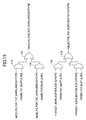
- FIGS. 8 through 11 are logic circuit diagrams showing important parts within the branch instruction controller 7 .
- AND circuits 171 through 173 and an OR circuit 174 generate a signal +RSBR_COMPLETE_TAKEN_RELEASE which becomes “1” when the control of at least one branch instruction which branches is completed in the branch instruction controller 7 .
- a signal +RDBR 0 _COMPLETE which becomes “1” when the control of the branch instruction at the 0th entry of the branch instruction controller 7 is completed, and a signal +RSBR 0 _TAKEN which becomes “1” when the branching of the branch instruction at the 0th entry of the branch instruction controller 7 becomes definite, are input to the AND circuit 171 .
- a signal +RDBR 1 _COMPLETE which becomes “1” when the control of the branch instruction at the 1st entry of the branch instruction controller 7 is completed, and a signal +RSBR 1 _TAKEN which becomes “1” when the branching of the branch instruction at the 1st entry of the branch instruction controller 7 becomes definite, are input to the AND circuit 172 .
- a signal +RDBR 2 _COMPLETE which becomes “1” when the control of the branch instruction at the 2nd entry of the branch instruction controller 7 is completed, and a signal +RSBR 2 _TAKEN which becomes “1” when the branching of the branch instruction at the 2nd entry of the branch instruction controller 7 becomes definite are input to the AND circuit 173 . Outputs of the AND circuits 171 through 173 are input to the OR circuit 174 .
- An exclusive-NOR circuit 271 and AND circuits 272 and 273 compare the IID of the branch instruction held in the entry A within the branching destination address register 10 within the branch instruction controller 7 and the IID of the branch instruction which branches when this branch instruction is committed.
- a signal +COMIT_TAKEN_IID[5:0] which indicates the IID of the branch instruction which branches when this branch instruction is committed within the branch instruction controller 7 (or the program counter section 11 ), and a signal +RSBR_TGT_BUFF_A_IID[5:0] which indicates the IID of the branch instruction which is held in the entry A of the branching destination address register 10 and is within the branch instruction controller 7 , are input to the exclusive-NOR circuit 271 .
- the signal +RSBR_TGT_BUFF_A_IID[5:0] is equivalent to a signal +TARGET_ADRS_BUFFER_A_IID[5:0] which will be described later.
- a signal +LOAD_TGT_TO_NPC which becomes “1” when it is necessary to set a value in the next program counter nPC from the branching destination address register 10 and a signal +RSBR_TGT_BUFF_A_VALID which becomes “1” when the entry A within the branching destination address register 10 is valid, are input to the AND circuit 272 .
- Outputs of the exclusive-NOR circuit 271 and the AND circuit 272 are input to the AND circuit 273 .
- An exclusive-NOR circuit 274 and AND circuits 275 and 276 compare the IID of the branch instruction held in the entry B within the branching destination address register 10 within the branch instruction controller 7 and the IID of the branch instruction which branches when this branch instruction is committed.
- the signal +RSBR_TGT_BUFF_B_IID[5:0] is equivalent to a signal +TARGET_ADRS_BUFFER_B_IID[5:0] which will be described later.
- the signal +LOAD_TGT_TO_NPC which becomes “1” when it is necessary to set a value in the next program counter nPC from the branching destination address register 10 , and a signal +RSBR_TGT_BUFF_B_VALID which becomes “1” when the entry B within the branching destination address register 10 is valid, are input to the AND circuit 275 .
- Outputs of the exclusive-NOR circuit 274 and the AND circuit 275 are input to the AND circuit 276 .
- an AND circuit 277 generates a clock enable signal +HOLD_RSBR_TGT_BUFF_A with respect to the entry A of the branching destination address register 10 , based on a signal ⁇ RSBR_TGT_BUFF_A_REL which becomes “1” when releasing the entry A of the branching destination address register 10 and a signal +RSBR_TGT_BUFF_A_VALID which becomes “1” when the entry A within the branching destination address register 10 is valid.
- An AND circuit 278 generates a clock enable signal +HOLD_RSBR_TGT_BUFF_B with respect to the entry B of the branching destination address register 10 , based on a signal ⁇ RSBR_TGT_BUFF_B_REL which becomes “1” when releasing the entry B of the branching destination address register 10 and a signal +RSBR_TGT_BUFF_B_VALID which becomes “1” when the entry B within the branching destination address register 10 is valid.
- a NAND circuit 371 generates a signal ⁇ RSBR 0 _TGT_BUFF_BUSY which indicates that no vacant entry exists in the branching destination address register 10 when the branch instruction at the 0th entry of the branch instruction controller 7 is a branch instruction which branches, based on a signal +RSBR 0 _TAKEN which becomes “1” when the branching of the branch instruction at the 0th entry of the branch instruction controller 7 becomes definite, the signal +RSBR_TGT_BUFF_A_VALID which becomes “1” when the entry A within the branching destination address register 10 is valid, the signal +RSBR_TGT_BUFF_B_VALID which becomes “1” when the entry B within the branching destination address register 10 is valid, and a signal ⁇ W_COMMIT_BR_TAKEN which indicates that the branch instruction which branches is committed.
- the signal ⁇ W_COMMIT_BR_TAKEN is a signal in the cycle W, and becomes “1” with a cycle corresponding to when the branch instruction which branches
- a NAND circuit 372 generates a signal ⁇ RSBR 1 _TGT_BUFF_BUSY which indicates that no vacant entry exists in the branching destination address register 10 when the branch instruction at the 1st entry of the branch instruction controller 7 is a branch instruction which branches, based on a signal +RSBR 1 _TAKEN which becomes “1” when the branching of the branch instruction at the 1st entry of the branch instruction controller 7 becomes definite, the signal +RSBR_TGT_BUFF_A_VALID which becomes “1” when the entry A within the branching destination address register 10 is valid, the signal +RSBR_TGT_BUFF_B_VALID which becomes “1” when the entry B within the branching destination address register 10 is valid, and a signal ⁇ W_COMMIT_BR_TAKEN which indicates that the branch instruction which branches is committed.
- the signal ⁇ W_COMMIT_BR_TAKEN is a signal in the cycle W, and becomes “1” with the cycle corresponding to when the branch instruction which branches is committed plus
- a NAND circuit 373 generates a signal ⁇ RSBR 2 _TGT_BUFF_BUSY which indicates that no vacant entry exists in the branching destination address register 10 when the branch instruction at the 0th entry of the branch instruction controller 7 is a branch instruction which branches, based on a signal +RSBR 2 _TAKEN which becomes “1” when the branching of the branch instruction at the 2nd entry of the branch instruction controller 7 becomes definite, the signal +RSBR_TGT_BUFF_A_VALID which becomes “1” when the entry A within the branching destination address register 10 is valid, the signal +RSBR_TGT_BUFF_B_VALID which becomes “1” when the entry B within the branching destination address register 10 is valid, and a signal ⁇ W_COMMIT_BR_TAKEN which indicates that the branch instruction which branches is committed.
- the signal +W_COMMIT_BR_TAKEN is a signal in the cycle W, and becomes “1” with the cycle corresponding to when the branch instruction which branches is committed plus (+)
- a signal +RSBR_COMPLETE_TAKEN_RELEASE is input to a set terminal SET of a latch circuit 374
- a signal ⁇ CLEAR_PIPELINE which indicates that all instructions in the executing pipeline are to be cleared is input to an input terminal INHS of the latch circuit 374 .
- the signals +RSBR_TGT_BUFF_A_REL and +CLEAR_PIPELINE are input to a NOR circuit 375 , and an output of this NOR circuit 375 is input to a reset terminal RST of the latch circuit 374 .
- the latch circuit 374 generates the signal +RSBR_TGT_BUFF_A_VALID described above.
- the signal +RSBR_COMPLETE_TAKEN_RELEASE and the clock enable signal +HOLD_RSBR_TGT_BUFF_A are input to an AND circuit 377 , and an output of this AND circuit 377 is input to a set terminal SET of a latch circuit 376 .
- the signal ⁇ CLEAR_PIPELINE which indicates that all instructions in the executing pipeline are to be cleared is input to an input terminal INHS of the latch circuit 376 .
- the signals +RSBR_TGT_BUFF_B_REL and +CLEAR_PIPELINE are input to a NOR circuit 378 , and an output of this NOR circuit 378 is input to a reset terminal RST of the latch circuit 376 .
- the latch circuit 376 generates the signal +RSBR_TGT_BUFF_B_VALID described above.
- the signals +HOLD_RSBR_TGT_BUFF_A, +COMPLETE_RSBR_IID[5:0], +COMPLETE_RSBR_CARRY, +COMPLETE_RSBR_BORROW and +COMPLETE_RSBR_TGT_PC[31:0,P3:P0] are input to a latch circuit 471 , and signals +TARGET_ADRS_BUFFER_A_IID[5:0], +TARGET_ADRS_BUFFER_A_OVF, +TARGET_ADRS_BUFFER_A_UDF and +TARGET_ADRS_A_BUFFER_A[31:0,P3:P0] are output from the latch circuit 471 .
- the signal +HOLD_RSBR_TGT_BUFF_A is a clock enable signal for the entry A of the branching destination address register 10
- the signal +COMPLETE_RSBR_IID[5:0] is the IID of the branch instruction which is released (when the control of the branch instruction is completed) from the branch instruction controller 7
- the signal +COMPLETE_RSBR_CARRY becomes “1” when a carry is generated at the branching destination address of the branch instruction which is released from the branch instruction controller 7
- the signal +COMPLETE_RSBR_BORROW becomes “1” when a borrow is generated at the branching destination address of the branch instruction which is released from the branch instruction controller 7 .
- the signal +COMPLETE_RSBR_TGT_PC[31:0,P3:P0] is the branching destination address of the branch instruction which is released from the branch instruction controller 7 .
- the signal +TARGET_ADRS_BUFFER_A_IID[5:0] is the IID of the branch instruction which is held in the entry A of the branching destination address register 10 .
- the signal +TARGET_ADRS_BUFFER_A_OVF is the carry bit (CARRY) of the branch instruction held in the entry A of the branching destination address register 10
- the signal +TARGET_ADRS_BUFFER_A_UDF is the borrow bit (BORROW) of the branch instruction held in the entry A of the branching destination address register 10 .
- the signal +TARGET_ADRS_BUFFER_A[31:0,P3:P0] is the branching destination address of the branch instruction held in the entry A of the branching destination address register 10 .
- the signals +HOLD_RSBR_TGT_BUFF_B, +COMPLETE_RSBR_IID[5:0], +COMPLETE_RSBR_CARRY, +COMPLETE_RSBR_BORROW and +COMPLETE_RSBR_TGT_PC[31:0,P3:P0] are input to a latch circuit 472 , and signals +TARGET_ADRS_BUFFER_B_IID[5:0], +TARGET_ADRS_BUFFER_B_OVF, +TARGET_ADRS_BUFFER_B_UDF and +TARGET_ADRS_B_BUFFER_A[31:0,P3:P0] are output from the latch circuit 472 .
- the signal +HOLD_RSBR_TGT_BUFF_B is a clock enable signal for the entry B of the branching destination address register 10
- the signal +COMPLETE_RSBR_IID[5:0] is the IID of the branch instruction which is released (when the control of the branch instruction is completed) from the branch instruction controller 7
- the signal +COMPLETE_RSBR_CARRY becomes “1” when a carry is generated at the branching destination address of the branch instruction which is released from the branch instruction controller 7
- the signal +COMPLETE_RSBR_BORROW becomes “1” when a borrow is generated at the branching destination address of the branch instruction which is released from the branch instruction controller 7 .
- the signal +COMPLETE_RSBR_TGT_PC[31:0,P3:P0] is the branching destination address of the branch instruction which is released from the branch instruction controller 7 .
- the signal +TARGET_ADRS_BUFFER_B_IID[5:0] is the IID of the branch instruction which is held in the entry B of the branching destination address register 10 .
- the signal +TARGET_ADRS_BUFFER_B_OVF is the carry bit (CARRY) of the branch instruction held in the entry B of the branching destination address register 10
- the signal +TARGET_ADRS_BUFFER_B_UDF is the borrow bit (BORROW) of the branch instruction held in the entry B of the branching destination address register 10 .
- the signal +TARGET_ADRS_BUFFER_B[31:0,P3:P0] is the branching destination address of the branch instruction held in the entry B of the branching destination address register 10 .
- FIGS. 12 and 13 are logic circuit diagrams showing important parts within the instruction completion controller 9 .
- a signal +4TH_CSE_BR_FORCE_NOP which becomes “1” when the instruction which is committed fourth is the branch instruction and the subsequent delay instruction is to be annulled, and a signal +COMMIT — 4TH_CSE which indicates that at least four instructions are committed are input to an AND circuit 94 . Outputs of the AND circuits 91 through 94 are input to a NOR circuit 95 .
- a signal ⁇ RS 1 which becomes “1” when an interrupt process is generated, and a signal +BR_FORCE_NOP_TGR which indicates that the next instruction which is first committed is the delay instruction which is changed to the NOP instruction are input to an AND circuit 96 .
- a signal ⁇ COMMIT_TOQ_CSE which indicates that at least one instruction is committed, and an output of the AND circuit 96 are input to a NAND circuit 97 .
- Outputs of the NOR circuit 95 and the NAND circuit 97 are input to an AND circuit 98 .
- a signal +EU_XCPTN_OR which becomes “1” when an exception is generated in the execution unit 23 or the like is input to an input terminal 1 H of a latch circuit 99 .
- An output of the AND circuit 98 is input to a set terminal SET of the latch circuit 99 .
- a signal ⁇ BR_FORCE_NOP_TGR which indicates that the next instruction which is committed first is the delay instruction which is changed to the NOP instruction is output from the latch circuit 99 .
- a signal +WTRAP_VALID of the cycle W indicating that an instruction which carries out a trap process
- a signal +COMMIT_ENDOP_OR which indicates that at least one instruction is committed are input to a NAND circuit 191 .
- An output of the AND circuit 192 is input to a set terminal SET of the latch circuit 193 .
- the latch circuit 193 outputs a signal +FORCE_PC_INCR_TGR.
- the signal +FORCE_PC_INCR_TGR becomes “1” when the branch instruction is committed, the time until the delay slot instruction is committed is delayed and the program counter PC and the next program counter nPC must be updated by an amount corresponding to the delay slot instruction (4 bytes) when the interrupt process is generated.
- the signal +FORCE_PC_INCR_TGR rises after 1 ⁇ from the signal +FORCE_NOP_TGR, and becomes valid in a cycle W+1.
- FIGS. 14 through 18 are logic circuit diagrams showing the updating circuit 11 - 3 within the program counter section 11 .
- the signals +PC[63:32,P7:P4], +TARGET_ADRS_BUFFER_A_OVF and +TARGET_ADRS_BUFFER_A_UDF are input to an incrementor 111 , and a signal +MOD_PC_FOR_TGT_ADRS_A[63:32,P7:P4] is output from the incrementor 111 .
- the signal +MOD_PC_FOR_TGT_ADRS_A[63:32,P7:P4] indicates the upper portion of the branching destination address when the carry bit (CARRY) or the borrow bit (BORROW) is “1” in the entry A of the branching destination address register 10 .
- the signals +PC[63:32,P7:P4], +TARGET_ADRS_BUFFER_B_OVF and +TARGET_ADRS_BUFFER_B_UDF are input to an incrementor 112 , and a signal +MOD_PC_FOR_TGT_ADRS_B[63:32,P7:P4] is output from the incrementor 112 .
- the signal +MOD_PC_FOR_TGT_ADRS_B[63:32,P7:P4] indicates the upper portion of the branching destination address when the carry bit (CARRY) or the borrow bit (BORROW) is “1” in the entry B of the branching destination address register 10 .
- the signals +MOD_PC_FOR_TGT_ADRS_A[63:32,P7:P4] and +RSBR_TGT_BUFF_A_REL are input to an AND circuit 113
- the signals +MOD_PC_FOR_TGT_ADRS_B[63:32,P7:P4] and +RSBR_TGT_BUFF_B_REL are input to an AND circuit 114 .
- An OR circuit 115 outputs a signal +MOD_PC_FOR_TGT_ADRS[63:32,P7:P4] based on outputs of the AND circuits 113 and 114 .
- the signal +MOD_PC_FOR_TGT_ADRS[63:32,P7:P4] indicates the upper portion of the branching destination address which is set from the branching destination address register 10 to the next program counter nPC.
- the signals +TARGET_ADRS_BUFFER_A[31:0,P3:P0] and +RSBR_TGT_BUFF_A_REL are input to an AND circuit 116 , and signals +TARGET_ADRS_BUFFER_B[31:0,P3:P0] and +RSBR_TGT_BUFF_B_REL are input to an AND circuit 117 .
- An OR circuit 118 outputs a signal +SELECTED_TGT_ADRS_BUFF[31:0,P3:P0] based on outputs of the AND circuits 116 and 117 .
- the signal +SELECTED_TGT_ADRS_BUFF[31:0,P3:P0] indicates the lower portion of the branching destination address which is set from the branching destination address register 10 to the next program counter nPC.
- the signals +NPC[63:0,P7:P0], +NPC_INCREMENT[3:0] and +FORCE_PC_INCR_TGR are input to an incrementor 211 , and the incrementor 211 outputs a signal +INCR_NPC[63:0,P7:P0].
- the signal +NPC_INCREMENT[3:0] indicates the number of instructions which are committed simultaneously. For example, if bit 3 is “1”, it is indicated that four instructions were committed simultaneously, and if bit 2 is “1”, it is indicated that three instructions were committed simultaneously.
- signals +COMMIT_UPDATE_PC and ⁇ RS 1 are input to an AND circuit 212 .
- the signal +COMMIT_UPDATE_PC indicates that the program counter PC or the next program counter nPC needs to be updated.
- An output of the AND circuit 212 , and signals +TRAP_SW 1 and +FORCE_PC_INCR_TGR are input to a NOR circuit 213 .
- An output of the NOR circuit 213 is used as a clock enable signal ⁇ CE_NPC of the next program counter nPC and as a clock enable signal ⁇ CE_PC of the program counter PC.
- signals +COMMIT_UPDATE_PC, ⁇ BRTKN_EQ_JUMPL_HOLD_VALID and ⁇ LOAD_TARGET_ADRS_TO_NPC are input to an AND circuit 214 .
- the signal ⁇ BRTKN_EQ_JUMPL_HOLD_VALID becomes “1” when the upper portion of the branching address of the register relative branch instruction which is committed is not all 0 (All 0) and is held in the latch circuit 11 - 1 .
- An output of the AND circuit 214 and the signal +FORCE_PC_INCR_TGR are input to an OR circuit 215 .
- An output signal +SEL_INCR_TO_NPC_LOW of the OR circuit 215 and a signal ⁇ PSTATE_AM are input to an AND circuit 216 .
- the signal +SEL_INCR_TO_NPC_LOW becomes “1” when selecting the signal +INCR_NPC upon setting to the lower portion of the next program counter nPC.
- the signal ⁇ PSTATE_AM indicates a 32-bit address mode when “1”.
- the AND circuit 216 outputs a signal +SEL_INCR_TO_NPC_HIGH. This signal +SEL_INCR_TO_NPC_HIGH becomes “1” when selecting the signal +INCR_NPC upon setting to the upper portion of the next program counter nPC.
- the signals ⁇ BRTKN_EQ_JUMPL_HOLD_VALID and +LOAD_TARGET_ADRS_TO_NPC are input to an AND circuit 217 .
- An output of the AND circuit 217 and the signal +FORCE_PC_INCR_TGR are input to an OR circuit 218 .
- An output of the OR circuit 218 and the signal ⁇ PSTATE_AM are input to an AND circuit 219 .
- the AND circuit 219 outputs a signal +SEL_TARGET_TO_NPC_HIGH.
- the signal +SEL_TARGET_TO_NPC_HIGH becomes “1” when selecting the signal +MOD_PC_FOR_TGT_ADRS upon setting to the higher portion of the next program counter nPC.
- a buffer 311 outputs a signal +SEL_TARGET_TO_NPC_LOW based on a signal +LOAD_TARGET_ADRS_TO_NPC.
- the signal +LOAD_TARGET_ADRS_TO_NPC becomes “1” when it is necessary to set a value from the branching destination address register 10 to the next program counter nPC.
- the +SEL_TARGET_TO_NPC_LOW becomes “1” when selecting the signal +SELECTED_TGT?ADRS_BUFF upon setting to the upper portion of the next program counter nPC.
- An AND circuit 312 outputs a signal +SEL_JUMPL_AH_TO_NPC based on the signals +BRTKN_EQ_JUMPL_HOLD_TGR and ⁇ PSTATE_AM.
- the signal +SEL_JUMPL_AH_TO_NPC becomes “1” when selecting a value (+JMPL_ADRS_HOLD) from the latch circuit 11 - 1 upon setting to the upper portion of the next program counter nPC.
- the signals +INCR_MPC[63:32,P7:P4] and +SEL_INCR_TO_NPC_HIGH are input to an AND circuit 411
- the signals +MOD_PC_FOR_TGT_ADRS[63:32,P7:P4] and +SEL_TARGET_TO_NPC_HIGH are input to an AND circuit 412
- the signals +JUMPL_ADRS_HOLD[63:32,P7:P4] and +SEL_JUMPL_AH_TO_NPC are input to an AND circuit 413
- the signals +TRAP_ADRS[63:32,P7:P4] and +SEL_TRAP_ADRS_TO_NPC are input to an AND circuit 414 .
- the signal +SEL_TRAP_ADRS_TO_NPC becomes “1” when selecting the signal +TRAP_ADRS upon generation of the trap.
- An OR circuit 415 outputs a set signal +SET_NPC[63:32,P7:P4] of the next program counter nPC based on outputs of the AND circuits 411 through 414 .
- Signals +INCR_NPC[31:0,P3:P0] and +SEL_INCR — TO_NPC_LOW are input to an AND circuit 416 , and signals +SELECTED_TGT_ADRS_BUFF[31:0,P3:P0] and +SEL_TARGET_TO_NPC_LOW are input to an AND circuit 417 .
- Signals +TRAP_ADRS[31:0,P3:P0] and +SEL_TRAP_ADRS_TO_NPC are input to an AND circuit 418 .
- An OR circuit 419 outputs a signal +SET_NPC[31:0,P3:P0] based on outputs of the AND circuits 416 through 418 .
- FIGS. 19 and 20 are logic circuit diagrams showing the updating circuit 11 - 2 within the program counter section 11 .
- the signals +COMMIT_UPDATE_PC and +FORCE_PC_INCR_TGR are input to an OR circuit 511 .
- An output signal +SEL_INCR_TO_PC_LOW of the OR circuit 511 and the signal ⁇ PSTATE_AM are input to an AND circuit 512 .
- the signal +SEL_INCR_TO_PC_LOW becomes “1” when selecting the signal +INCR_PC upon setting to the lower portion of the program counter PC.
- the signals +PC[63:0,P7:P0], +NPC_INCREMENT[3:0] and +FORCE_PC_INCR_TGR are input to an incrementor 513 , and the incrementor 513 outputs a signal +INCR_PC[63:0,P7:P0].
- signals +INCR_PC[63:32,P7:P4] and +SEL_INCR_TO_PC_HIGH are input to an AND circuit 611
- signals +TRAP_ADRS[63:32,P7:P4] and +SEL_TRAP_ADRS_TO_PC are input to an AND circuit 612 .
- the signal +SEL_TRAP_ADRS_TO_PC becomes “1” when selecting the signal +TRAP_ADRS upon generation of the trap.
- An OR circuit 613 outputs a set signal +SET_PC[63:32,P7:P4] for the program counter PC, based on outputs of the AND circuits 611 and 612 .
- Signals +INCR_PC[31:0,P3:P0] and +SEL_INCR_TO_PC_LOW are input to an AND circuit 614
- signals +TRAP_ADRS[31:0,P3:P0] and +SEL_TRAP_ADRS_TO_PC are input to an AND circuit 615 .
- An OR circuit 616 outputs a set signal +SET_PC[31:0,P3:P0] for the program counter PC, based on outputs of the AND circuits 614 and 615 .
- the branching destination address register is provided, and the instruction address register is updated at a high speed depending on the number of simultaneously committed instructions.
- the control of the branch instruction can be made independently in the branch instruction controller, the branch predictor, the branching destination address register and the instruction completion controller, it is possible to improve the throughput of the branching and realize a circuit having a minimum assembling area.
Landscapes
- Engineering & Computer Science (AREA)
- Software Systems (AREA)
- Theoretical Computer Science (AREA)
- Physics & Mathematics (AREA)
- General Engineering & Computer Science (AREA)
- General Physics & Mathematics (AREA)
- Advance Control (AREA)
Applications Claiming Priority (3)
| Application Number | Priority Date | Filing Date | Title |
|---|---|---|---|
| JP2002-190557 | 2002-06-28 | ||
| JPPAT.A2002-190557 | 2002-06-28 | ||
| JP2002190557A JP3800533B2 (ja) | 2002-06-28 | 2002-06-28 | プログラムカウンタ制御方法及びプロセッサ |
Publications (2)
| Publication Number | Publication Date |
|---|---|
| US20040003207A1 US20040003207A1 (en) | 2004-01-01 |
| US7765387B2 true US7765387B2 (en) | 2010-07-27 |
Family
ID=29774332
Family Applications (1)
| Application Number | Title | Priority Date | Filing Date |
|---|---|---|---|
| US10/352,005 Expired - Fee Related US7765387B2 (en) | 2002-06-28 | 2003-01-28 | Program counter control method and processor thereof for controlling simultaneous execution of a plurality of instructions including branch instructions using a branch prediction mechanism and a delay instruction for branching |
Country Status (2)
| Country | Link |
|---|---|
| US (1) | US7765387B2 (ja) |
| JP (1) | JP3800533B2 (ja) |
Cited By (7)
| Publication number | Priority date | Publication date | Assignee | Title |
|---|---|---|---|---|
| US8868886B2 (en) | 2011-04-04 | 2014-10-21 | International Business Machines Corporation | Task switch immunized performance monitoring |
| US9015449B2 (en) | 2011-03-27 | 2015-04-21 | International Business Machines Corporation | Region-weighted accounting of multi-threaded processor core according to dispatch state |
| US9189365B2 (en) | 2011-08-22 | 2015-11-17 | International Business Machines Corporation | Hardware-assisted program trace collection with selectable call-signature capture |
| US9342432B2 (en) | 2011-04-04 | 2016-05-17 | International Business Machines Corporation | Hardware performance-monitoring facility usage after context swaps |
| US10198260B2 (en) | 2016-01-13 | 2019-02-05 | Oracle International Corporation | Processing instruction control transfer instructions |
| US20200371811A1 (en) * | 2019-05-23 | 2020-11-26 | Samsung Electronics Co., Ltd. | Branch prediction throughput by skipping over cachelines without branches |
| US11106466B2 (en) * | 2018-06-18 | 2021-08-31 | International Business Machines Corporation | Decoupling of conditional branches |
Families Citing this family (3)
| Publication number | Priority date | Publication date | Assignee | Title |
|---|---|---|---|---|
| DE602006013515D1 (de) * | 2006-02-28 | 2010-05-20 | Fujitsu Ltd | Verarbeitungseinrichtung durch vorhersage einer abzweigung aus komprimierten adresseninformationen |
| EP2996034B1 (en) * | 2014-09-11 | 2018-08-15 | Nxp B.V. | Execution flow protection in microcontrollers |
| WO2018182746A1 (en) * | 2017-04-01 | 2018-10-04 | Intel Corporation | Hotpluggable runtime |
Citations (13)
| Publication number | Priority date | Publication date | Assignee | Title |
|---|---|---|---|---|
| JPH03122718A (ja) | 1989-10-05 | 1991-05-24 | Fujitsu Ltd | パイプライン計算機における条件分岐命令実行制御方式 |
| JPH04213727A (ja) | 1990-12-12 | 1992-08-04 | Matsushita Electric Ind Co Ltd | 情報処理装置 |
| JPH0540627A (ja) | 1990-09-05 | 1993-02-19 | Toshiba Corp | 並列演算処理装置 |
| US5265213A (en) | 1990-12-10 | 1993-11-23 | Intel Corporation | Pipeline system for executing predicted branch target instruction in a cycle concurrently with the execution of branch instruction |
| JPH0793151A (ja) | 1993-09-21 | 1995-04-07 | Oki Electric Ind Co Ltd | 命令供給装置 |
| JPH07262008A (ja) | 1994-03-25 | 1995-10-13 | Fujitsu Ltd | 並列分岐処理装置 |
| US5515519A (en) * | 1993-03-19 | 1996-05-07 | Hitachi, Ltd. | Data processor and method utilizing coded no-operation instructions |
| US5640588A (en) * | 1991-05-15 | 1997-06-17 | Ross Technology, Inc. | CPU architecture performing dynamic instruction scheduling at time of execution within single clock cycle |
| US5784603A (en) * | 1996-06-19 | 1998-07-21 | Sun Microsystems, Inc. | Fast handling of branch delay slots on mispredicted branches |
| US5826074A (en) * | 1996-11-22 | 1998-10-20 | S3 Incorporated | Extenstion of 32-bit architecture for 64-bit addressing with shared super-page register |
| US5867683A (en) * | 1993-10-29 | 1999-02-02 | Advanced Micro Devices, Inc. | Method of operating a high performance superscalar microprocessor including a common reorder buffer and common register file for both integer and floating point operations |
| US6240510B1 (en) * | 1998-08-06 | 2001-05-29 | Intel Corporation | System for processing a cluster of instructions where the instructions are issued to the execution units having a priority order according to a template associated with the cluster of instructions |
| US6883090B2 (en) * | 2001-05-17 | 2005-04-19 | Broadcom Corporation | Method for cancelling conditional delay slot instructions |
-
2002
- 2002-06-28 JP JP2002190557A patent/JP3800533B2/ja not_active Expired - Fee Related
-
2003
- 2003-01-28 US US10/352,005 patent/US7765387B2/en not_active Expired - Fee Related
Patent Citations (15)
| Publication number | Priority date | Publication date | Assignee | Title |
|---|---|---|---|---|
| JPH03122718A (ja) | 1989-10-05 | 1991-05-24 | Fujitsu Ltd | パイプライン計算機における条件分岐命令実行制御方式 |
| US5461722A (en) | 1990-09-05 | 1995-10-24 | Kabushiki Kaisha Toshiba | Parallel processing apparatus suitable for executing in parallel a plurality of instructions including at least two branch instructions |
| JPH0540627A (ja) | 1990-09-05 | 1993-02-19 | Toshiba Corp | 並列演算処理装置 |
| US5265213A (en) | 1990-12-10 | 1993-11-23 | Intel Corporation | Pipeline system for executing predicted branch target instruction in a cycle concurrently with the execution of branch instruction |
| JPH06110683A (ja) | 1990-12-10 | 1994-04-22 | Intel Corp | マイクロプロセッサの拡張ブランチターゲット方法及びその装置 |
| JPH04213727A (ja) | 1990-12-12 | 1992-08-04 | Matsushita Electric Ind Co Ltd | 情報処理装置 |
| US5640588A (en) * | 1991-05-15 | 1997-06-17 | Ross Technology, Inc. | CPU architecture performing dynamic instruction scheduling at time of execution within single clock cycle |
| US5515519A (en) * | 1993-03-19 | 1996-05-07 | Hitachi, Ltd. | Data processor and method utilizing coded no-operation instructions |
| JPH0793151A (ja) | 1993-09-21 | 1995-04-07 | Oki Electric Ind Co Ltd | 命令供給装置 |
| US5867683A (en) * | 1993-10-29 | 1999-02-02 | Advanced Micro Devices, Inc. | Method of operating a high performance superscalar microprocessor including a common reorder buffer and common register file for both integer and floating point operations |
| JPH07262008A (ja) | 1994-03-25 | 1995-10-13 | Fujitsu Ltd | 並列分岐処理装置 |
| US5784603A (en) * | 1996-06-19 | 1998-07-21 | Sun Microsystems, Inc. | Fast handling of branch delay slots on mispredicted branches |
| US5826074A (en) * | 1996-11-22 | 1998-10-20 | S3 Incorporated | Extenstion of 32-bit architecture for 64-bit addressing with shared super-page register |
| US6240510B1 (en) * | 1998-08-06 | 2001-05-29 | Intel Corporation | System for processing a cluster of instructions where the instructions are issued to the execution units having a priority order according to a template associated with the cluster of instructions |
| US6883090B2 (en) * | 2001-05-17 | 2005-04-19 | Broadcom Corporation | Method for cancelling conditional delay slot instructions |
Non-Patent Citations (4)
| Title |
|---|
| Computer Organization and Design. * |
| Japanese Office Action dated Jan. 24, 2006 of Japanese Application No. 2002-190556. |
| SPARC International Inc., "The SPARC Architecture Manual," Version 8, Revision SAV080SI9308, 1992 (pp. 3, 12, 32, 43, 50-53, 62, 63, and 134). |
| U.S. Appl. No. 10/345,296, filed Jan. 16, 2003, Ryuichi Sunayama, Fujitsu Limited Kawasaki, Japan. |
Cited By (9)
| Publication number | Priority date | Publication date | Assignee | Title |
|---|---|---|---|---|
| US9015449B2 (en) | 2011-03-27 | 2015-04-21 | International Business Machines Corporation | Region-weighted accounting of multi-threaded processor core according to dispatch state |
| US9110708B2 (en) | 2011-03-27 | 2015-08-18 | International Business Machines Corporation | Region-weighted accounting of multi-threaded processor core according to dispatch state |
| US8868886B2 (en) | 2011-04-04 | 2014-10-21 | International Business Machines Corporation | Task switch immunized performance monitoring |
| US9342432B2 (en) | 2011-04-04 | 2016-05-17 | International Business Machines Corporation | Hardware performance-monitoring facility usage after context swaps |
| US9189365B2 (en) | 2011-08-22 | 2015-11-17 | International Business Machines Corporation | Hardware-assisted program trace collection with selectable call-signature capture |
| US10198260B2 (en) | 2016-01-13 | 2019-02-05 | Oracle International Corporation | Processing instruction control transfer instructions |
| US11106466B2 (en) * | 2018-06-18 | 2021-08-31 | International Business Machines Corporation | Decoupling of conditional branches |
| US20200371811A1 (en) * | 2019-05-23 | 2020-11-26 | Samsung Electronics Co., Ltd. | Branch prediction throughput by skipping over cachelines without branches |
| US11182166B2 (en) * | 2019-05-23 | 2021-11-23 | Samsung Electronics Co., Ltd. | Branch prediction throughput by skipping over cachelines without branches |
Also Published As
| Publication number | Publication date |
|---|---|
| US20040003207A1 (en) | 2004-01-01 |
| JP2004038256A (ja) | 2004-02-05 |
| JP3800533B2 (ja) | 2006-07-26 |
Similar Documents
| Publication | Publication Date | Title |
|---|---|---|
| US8464029B2 (en) | Out-of-order execution microprocessor with reduced store collision load replay reduction | |
| US7836287B2 (en) | Reducing the fetch time of target instructions of a predicted taken branch instruction | |
| US7117347B2 (en) | Processor including fallback branch prediction mechanism for far jump and far call instructions | |
| US6289445B2 (en) | Circuit and method for initiating exception routines using implicit exception checking | |
| US20060184738A1 (en) | Unaligned memory access prediction | |
| EP0448499A2 (en) | Instruction prefetch method for branch-with-execute instructions | |
| US5740393A (en) | Instruction pointer limits in processor that performs speculative out-of-order instruction execution | |
| US6912650B2 (en) | Pre-prefetching target of following branch instruction based on past history | |
| EP0094535B1 (en) | Pipe-line data processing system | |
| US7844806B2 (en) | Global history branch prediction updating responsive to taken branches | |
| US4739470A (en) | Data processing system | |
| US7765387B2 (en) | Program counter control method and processor thereof for controlling simultaneous execution of a plurality of instructions including branch instructions using a branch prediction mechanism and a delay instruction for branching | |
| US20040225870A1 (en) | Method and apparatus for reducing wrong path execution in a speculative multi-threaded processor | |
| US6502186B2 (en) | Instruction processing apparatus | |
| JP3725547B2 (ja) | 限定ラン分岐予測 | |
| US6754813B1 (en) | Apparatus and method of processing information for suppression of branch prediction | |
| US6920549B1 (en) | Branch history information writing delay using counter to avoid conflict with instruction fetching | |
| JP3779012B2 (ja) | 分岐による中断のないパイプライン化されたマイクロプロセッサ及びその動作方法 | |
| US7603545B2 (en) | Instruction control method and processor to process instructions by out-of-order processing using delay instructions for branching | |
| US6738897B1 (en) | Incorporating local branch history when predicting multiple conditional branch outcomes | |
| US20240118900A1 (en) | Arithmetic processing device and arithmetic processing method | |
| US11314505B2 (en) | Arithmetic processing device | |
| US6360310B1 (en) | Apparatus and method for instruction cache access | |
| JP3161711B2 (ja) | 情報処理装置 | |
| JP2022094507A (ja) | 演算処理回路及び演算処理方法 |
Legal Events
| Date | Code | Title | Description |
|---|---|---|---|
| AS | Assignment |
Owner name: FUJITSU LIMITED, JAPAN Free format text: ASSIGNMENT OF ASSIGNORS INTEREST;ASSIGNORS:SUNAYAMA, RYUICHI;MORITA, KUNIKI;INOUE, AIICHIRO;REEL/FRAME:013709/0715;SIGNING DATES FROM 20030109 TO 20030110 Owner name: FUJITSU LIMITED, JAPAN Free format text: ASSIGNMENT OF ASSIGNORS INTEREST;ASSIGNORS:SUNAYAMA, RYUICHI;MORITA, KUNIKI;INOUE, AIICHIRO;SIGNING DATES FROM 20030109 TO 20030110;REEL/FRAME:013709/0715 |
|
| STCF | Information on status: patent grant |
Free format text: PATENTED CASE |
|
| FEPP | Fee payment procedure |
Free format text: PAYOR NUMBER ASSIGNED (ORIGINAL EVENT CODE: ASPN); ENTITY STATUS OF PATENT OWNER: LARGE ENTITY |
|
| FPAY | Fee payment |
Year of fee payment: 4 |
|
| MAFP | Maintenance fee payment |
Free format text: PAYMENT OF MAINTENANCE FEE, 8TH YEAR, LARGE ENTITY (ORIGINAL EVENT CODE: M1552) Year of fee payment: 8 |
|
| FEPP | Fee payment procedure |
Free format text: MAINTENANCE FEE REMINDER MAILED (ORIGINAL EVENT CODE: REM.); ENTITY STATUS OF PATENT OWNER: LARGE ENTITY |
|
| LAPS | Lapse for failure to pay maintenance fees |
Free format text: PATENT EXPIRED FOR FAILURE TO PAY MAINTENANCE FEES (ORIGINAL EVENT CODE: EXP.); ENTITY STATUS OF PATENT OWNER: LARGE ENTITY |
|
| STCH | Information on status: patent discontinuation |
Free format text: PATENT EXPIRED DUE TO NONPAYMENT OF MAINTENANCE FEES UNDER 37 CFR 1.362 |
|
| FP | Lapsed due to failure to pay maintenance fee |
Effective date: 20220727 |