US7765367B2 - Control device for accelerating memory to execute iterant command - Google Patents
Control device for accelerating memory to execute iterant command Download PDFInfo
- Publication number
- US7765367B2 US7765367B2 US11/610,509 US61050906A US7765367B2 US 7765367 B2 US7765367 B2 US 7765367B2 US 61050906 A US61050906 A US 61050906A US 7765367 B2 US7765367 B2 US 7765367B2
- Authority
- US
- United States
- Prior art keywords
- state
- command
- memory
- state machine
- blocks
- Prior art date
- Legal status (The legal status is an assumption and is not a legal conclusion. Google has not performed a legal analysis and makes no representation as to the accuracy of the status listed.)
- Active, expires
Links
Images


Classifications
-
- G—PHYSICS
- G06—COMPUTING; CALCULATING OR COUNTING
- G06F—ELECTRIC DIGITAL DATA PROCESSING
- G06F13/00—Interconnection of, or transfer of information or other signals between, memories, input/output devices or central processing units
- G06F13/14—Handling requests for interconnection or transfer
- G06F13/16—Handling requests for interconnection or transfer for access to memory bus
- G06F13/1668—Details of memory controller
-
- Y—GENERAL TAGGING OF NEW TECHNOLOGICAL DEVELOPMENTS; GENERAL TAGGING OF CROSS-SECTIONAL TECHNOLOGIES SPANNING OVER SEVERAL SECTIONS OF THE IPC; TECHNICAL SUBJECTS COVERED BY FORMER USPC CROSS-REFERENCE ART COLLECTIONS [XRACs] AND DIGESTS
- Y02—TECHNOLOGIES OR APPLICATIONS FOR MITIGATION OR ADAPTATION AGAINST CLIMATE CHANGE
- Y02D—CLIMATE CHANGE MITIGATION TECHNOLOGIES IN INFORMATION AND COMMUNICATION TECHNOLOGIES [ICT], I.E. INFORMATION AND COMMUNICATION TECHNOLOGIES AIMING AT THE REDUCTION OF THEIR OWN ENERGY USE
- Y02D10/00—Energy efficient computing, e.g. low power processors, power management or thermal management
Definitions
- This invention is related to a semiconductor memory, especially a control device that can accelerate the memory to execute iterant commands.
- the present invention provides a control device of memory that accelerates memory to execute iterant commands.
- the control device can ease the work load on the micro-controller unit and increase the efficacy of memory when it executes commands.
- the present invention provides a control device of memory, which accelerates memory to execute iterant commands.
- This control device includes a micro-controller unit, a controller, a block information table and a state machine.
- the micro-controller unit is used to issue a command to operate the memory, which contains several blocks.
- the controller is coupled between the memory and the micro-controller. When the controller determines the command needs not be executed repeatedly, the micro-controller would issue the command through the control device. While the command is determined necessary for repetitive execution, the state machine would repeatedly carry out this command.
- the block information table is used to record the state of every block. The state machine obtains the information on the state of every block from the block information table to analyze the state of a block so as to repeatedly execute the said command, and update the state information in the block information table.
- the iterant command can be carried out without involving the micro-controller unit and a software, so as to improve the efficacy of the memory and lower its power consumption.
- FIG. 1 is a block diagram of a control device of a memory according to one embodiment of the present invention.
- FIG. 2 is a structure diagram of a block information table according to one embodiment of the invention.
- FIG. 3 is a state diagram of a state machine suitable for executing a command to search for several empty blocks according to one embodiment of the invention.
- FIG. 4 is a state diagram of a state machine according to one embodiment of the invention.
- FIG. 5 is a state diagram of a state machine during its execution of reading according to one preferred embodiment of the invention.
- FIG. 6 is a state diagram of a state machine during its execution of writing according to one preferred embodiment of the invention.
- FIG. 7 is a state diagram of a state machine during its execution of erasing according to one preferred embodiment of the invention.
- FIG. 1 is a block diagram of the control device of the memory according to one embodiment of the invention.
- a flash memory among non-volatile memories is used in this embodiment as an example, and the flash memory contains several blocks.
- a control device 100 is used for accelerating the flash memory to execute iterant commands, which includes a Micro-controller Unit 110 , a controller 120 , a state machine 130 , a block information table 140 and a queuer 150 .
- the micro-controller unit 110 issues a command to operate the memory.
- the said command can be a reading, writing, erasing command or a command to search for N empty blocks.
- N is a positive integer.
- the controller is coupled between the flash memory and the micro-controller unit 110 . When it determines the command needs not be executed repeatedly, the micro-controller unit 110 would issue the command through the controller 120 to carry out the said command. On the contrary, when the command is determined necessary for repetitive execution, the state machine 130 would repeatedly carry out this command.
- the state machine 130 when the state machine 130 is carrying out the command repeatedly, it also needs the block information table 140 and the queuer 150 .
- the block information table 140 is used to record the states of every block in the flash memory, while the queuer 150 is used to queue the addresses of the flash memory needed when the state machine 130 repeatedly executes the command.
- the state machine 130 obtains the states of each block in the flash memory through the block information table 140 , analyzes these states and repeatedly executes the command in proper execution, and then updates the corresponding states in the block information table 140 .
- the state machine 130 updates the corresponding state in the block information table 140 as a basis for restarting next time.
- FIG. 2 is an information structure diagram of the block information table according to one embodiment of the invention.
- the block information table 140 of FIG. 2 includes several sub-blocks information corresponding to every block in the flash memory respectively.
- the size of information of every block is 16 bits.
- the first column shown in two bits is used to record the state of the memory block, like three different states—empty, used and erasable.
- the second column is retained, not for ordinary use; it can be used to store the necessary information during expansion of other functions.
- the third column shown in 12 bits is used for LP mapping, i.e. the mapping relation from a logical address to a physical address.
- the information in every sub-block in the block information table 140 is built up according to the contents of the redundant area in the corresponding block inside the flash memory, and stored in a partitioned area in a RAM.
- the state machine 130 When the state machine 130 starts, it performs the corresponding execution according to an analysis result of the block states provided by the block information table 140 to carry out the command repeatedly, and the contents in the block information table 140 are updated by a software.
- the hardware will be based on the block state (the state values stored in the block state information table).
- the state machine 130 can be used to replace the micro-controller unit 110 to execute the command repetitively to significantly reduce the load on the micro-controller unit 110 and improve the efficacy of the whole flash memory. While it is not necessary to carry out the command, the state machine 130 enters an idle state to reduce its power consumption.
- FIG. 3 is the state diagram of a state machine according to an embodiment of this present invention; the device is suitable for executing the command to search for N empty blocks, wherein, N is a positive integer.
- the state machine 130 shown in FIG. 1 includes an idle state A, a searching state B, a determining state D, an erasure state D, a verification state E and an ending state F.
- the idle state A is the initial state of state machine 130 .
- the searching state B searches for N empty blocks from the flash memory based on the block states in the flash memory recorded in Block Information Table 140 .
- the determining state C is used to determine which blocks are empty or erasable.
- the erasure state D is used to erase the contents in the blocks.
- the verification state E is to verify whether or not the erasure of blocks is successfully completed.
- the ending state F is used to stop executing the command repetitively.
- the state machine 130 When the state machine 130 begins to receive signals, it means the command has to be executed repeatedly; hence, the state machine 130 enters the searching state B from the idle state A. Once the state machine 130 finds N empty blocks in the flash memory during the searching state B, it would enter the ending state F and stop repeatedly executing the command; oppositely, when the N empty blocks are not yet found, the state machine 130 would enter the determining state C.
- the state machine 130 determines the present blocks are empty or erasable according to the information in the state column of the sub-blocks during the determining state C. If the block is empty, its address will be recorded in the queuer 150 , and the state machine 130 will return to the searching state B to continue searching for the next empty block. If the block is erasable, the state machine 130 enters the erasure state D to erase it so that an erasure command can be directly issued from the hardware; there is no need to issue from the software. In addition, the state machine 130 enters the ending state F from the determining state C to stop executing the command repetitively, when the queuer 150 does not have enough space to queue addresses, or the number of times to repeat a command exceeds a preset number M, i.e. searching in M blocks without finding N empty blocks, wherein M is a positive integer larger than N.
- the state machine 130 When the contents in the blocks are erased, the state machine 130 enters the verification state E from the erasure State D to verify whether or not the erasure of blocks is successful. If so, the state machine 130 would return to the searching state B to look for the next empty block. If not, the state machine 130 would enter the ending state F to stop executing the command repeatedly. Lastly, the command of iterant execution is stopped during the ending state F, and the state is reported to the system. So in this embodiment, the state machine 130 can find the empty blocks in the flash memory that are still usable. If the number of usable empty blocks reaches the needed number, the state machine 130 would automatically stop in order to avoid wasting efficacy of the system and reduce power consumption. In addition, that no software is needed during the execution can also lower the load on the micro-controller unit 110 .
- FIG. 4 is a state diagram of a state machine according to another embodiment of this present invention.
- the device is suitable for iterant execution, such as erasure, writing-in, reading etc.
- the state machine awaits a firmware to issue a command in the idle state A, and then enters the searching state B.
- the searching state B When the condition of the searching is met, the state machine would enter the ending State F and report to the system.
- the state machine would enter the determining state C.
- the condition of the searching refers to that of ending this state machine. For example, if the state machine is set to erase 10 memory blocks, then the condition of the searching is 10 memory blocks.
- the state machine During the searching State B, if the state of the memory conforms to the condition, the state machine would enter the execution state D. On the contrary, if the state of the memory does not conform to the condition, then the state machine would return to the searching state B. Taking erasure for an example, if the state of the memory is labeled as erasable, the state machine would execute erasing it. If it is labeled as inerasable, the state machine would return to the searching state B.
- state machine When the execution of state D is completed, the state machine enters the verification state E. If the execution is carried out successfully, the state machine would return to the searching state B to continue carrying out the foregoing executions at the next address of the memory. Oppositely, if the execution fails, the state machine would return to the ending state F, and report to the system. Disclosed as follows is an example of a state machine during its executions of reading, writing-in and erasing.
- FIG. 5 is a state diagram of a state machine during its execution of reading according to one preferred embodiment of the invention.
- a wished execution is reading at a certain memory address in a certain memory block, first, marking the state corresponding to the targeted memory address as “to-be-read” through the firmware.
- the state machine 130 When the state machine 130 is started, the state machine would enter the searching state B from the idle state A.
- the state machine 130 would enter the determining state C. In the determining state C, the memory address and its state indicator are checked. Oppositely, when the designated memory blocks are all read, the state machine 130 would directly enter the ending state F.
- the state machine 130 would return to the searching state B, or re-check the next memory address and its state indicator. To the contrary, if the memory address is within the designated memory block and labeled as “to-be-read”, the state machine 130 would return to a reading execution state D. At this moment, the controller 120 is controlled to issue a reading command to the flash memory and returns to the verification state E when the controller 120 finishes performing the execution.
- the state machine 130 If the execution of reading the memory is successfully executed, the state machine 130 would return to the searching State B so as to continue repeating the above steps on the next memory address. Oppositely, if the execution of reading of the memory fails, the state machine would return to the ending state F, and report the state to the system. Therefore, in this embodiment, the state machine 130 can find the contents of a designated block within the flash memory and the system would automatically stop after the searching within the designated block is over. So that, the state machine 130 can share the load on the micro-controller unit 110 .
- FIG. 6 is a state diagram of a state machine during its execution of writing according to one preferred embodiment of the invention. Referring FIGS. 1 and 6 . If the desired execution is writing in a certain block in the memory, first, designating the desired address of the memory through a firmware for writing. When the state machine 130 is started, it would enter the searching state B from the idle state A. When the physical memory blocks are not yet fully written, the state machine 130 would enter the determining state C to check the memory address and its state indicator. Oppositely, when the designated memory blocks are all written, the state machine 130 would directly enter the ending state F.
- the state machine 130 While in the determining state C, if the memory address is not within the memory block to be written, or its state indicator labels “not-to-be-written”, the state machine 130 would return to the searching state B, or re-check the next memory address and its state indicator. Contrarily, if the memory address is within the designated memory block and labeled as “to-be-written”, the state machine 130 would return to a writing execution state D. At this moment, the system would issue a writing command to the flash memory through the controller 120 , and enter the verification state E after performance of the controller 120 .
- the state machine 130 If the execution for writing in the memory is successful, the state machine 130 would return to the searching state B so as to continue repeating the above steps on the next memory address. Oppositely, if the execution for writing in the memory fails, the state machine 130 would return to the ending state F, and report the state to the system. Hence, in this embodiment, the state machine 130 can execute iterant writing on the designated blocks according to the state indicator.
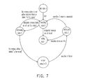
- FIG. 7 is a state diagram of a state machine during its execution of erasing according to one preferred embodiment of the invention.
- the desired execution is iterant erasure
- first labeling the state of the physical address of the to-be-erased memory as erasable in block information table 140 through a firmware.
- the state machine 130 After the state machine 130 is started, it would enter the searching state B. If all the designated blocks are not yet fully erased, the state machine 130 would enter the determining the determining state C. Oppositely, when the designated memory blocks are all erased, the state machine 130 would directly enter the ending state F.
- the state machine 130 would return to the searching state B to re-check the next memory address and its state indicator. Oppositely, if the address is within the designated block, and its state is labeled “erasable”, the state machine 130 would enter anthe erasure execution state D. At this moment, the controller 120 is controlled to issue an erasing command to the memory and returns to the verification state E when the controller 120 finishes performing the execution.
- the state machine 130 would return to the state B and repeat the above steps on the next memory address. Oppositely, if the execution of erasure fails, the state machine 130 would return to the ending state F, and report it to the system.
- the iterant command can be carried out without involving the micro-controller unit and software, so as to improve the efficacy of the memory and lower its power consumption.
Landscapes
- Engineering & Computer Science (AREA)
- Theoretical Computer Science (AREA)
- Physics & Mathematics (AREA)
- General Engineering & Computer Science (AREA)
- General Physics & Mathematics (AREA)
- Read Only Memory (AREA)
- Memory System (AREA)
- Information Retrieval, Db Structures And Fs Structures Therefor (AREA)
Applications Claiming Priority (3)
| Application Number | Priority Date | Filing Date | Title |
|---|---|---|---|
| TW95135520A | 2006-09-26 | ||
| TW95135520 | 2006-09-26 | ||
| TW095135520A TWI306255B (en) | 2006-09-26 | 2006-09-26 | Control device for accelerating memory to execute iterant command |
Publications (2)
| Publication Number | Publication Date |
|---|---|
| US20080077751A1 US20080077751A1 (en) | 2008-03-27 |
| US7765367B2 true US7765367B2 (en) | 2010-07-27 |
Family
ID=39226394
Family Applications (1)
| Application Number | Title | Priority Date | Filing Date |
|---|---|---|---|
| US11/610,509 Active 2028-07-05 US7765367B2 (en) | 2006-09-26 | 2006-12-14 | Control device for accelerating memory to execute iterant command |
Country Status (3)
| Country | Link |
|---|---|
| US (1) | US7765367B2 (ja) |
| JP (1) | JP4594944B2 (ja) |
| TW (1) | TWI306255B (ja) |
Cited By (2)
| Publication number | Priority date | Publication date | Assignee | Title |
|---|---|---|---|---|
| US8565021B2 (en) | 2008-06-13 | 2013-10-22 | Samsung Electronics Co., Ltd. | Memory system and method of accessing a semiconductor memory device |
| US9377966B2 (en) | 2013-10-09 | 2016-06-28 | Samsung Electronics Co., Ltd. | Method and apparatus for efficiently processing storage commands |
Families Citing this family (2)
| Publication number | Priority date | Publication date | Assignee | Title |
|---|---|---|---|---|
| TWI459203B (zh) * | 2012-10-02 | 2014-11-01 | Winbond Electronics Corp | 資料儲存裝置以及非揮發性記憶體控制方法 |
| TWI831366B (zh) * | 2022-09-08 | 2024-02-01 | 群聯電子股份有限公司 | 資料寫入方法、記憶體儲存裝置及記憶體控制電路單元 |
Citations (2)
| Publication number | Priority date | Publication date | Assignee | Title |
|---|---|---|---|---|
| US5034922A (en) * | 1987-12-21 | 1991-07-23 | Motorola, Inc. | Intelligent electrically erasable, programmable read-only memory with improved read latency |
| US20030226063A1 (en) * | 2002-05-31 | 2003-12-04 | Oracle International Corporation | Verifying input/output command data |
Family Cites Families (6)
| Publication number | Priority date | Publication date | Assignee | Title |
|---|---|---|---|---|
| JPH052529A (ja) * | 1991-06-24 | 1993-01-08 | Iwaki Electron Corp Ltd | フラツシユ・メモリのアクセス方法及びその回路 |
| JP3099908B2 (ja) * | 1991-08-09 | 2000-10-16 | 株式会社東芝 | Eepromの制御装置 |
| JPH096747A (ja) * | 1995-06-20 | 1997-01-10 | Ricoh Co Ltd | フラッシュメモリ制御装置 |
| JPH0991195A (ja) * | 1995-09-25 | 1997-04-04 | Kawasaki Steel Corp | ブロックメモリ管理装置 |
| JP2001006379A (ja) * | 1999-06-16 | 2001-01-12 | Fujitsu Ltd | 複写、移動機能を有するフラッシュメモリ |
| JP2003203486A (ja) * | 2002-01-08 | 2003-07-18 | Seiko Epson Corp | 半導体記憶装置及びその制御方法 |
-
2006
- 2006-09-26 TW TW095135520A patent/TWI306255B/zh active
- 2006-12-14 US US11/610,509 patent/US7765367B2/en active Active
-
2007
- 2007-02-07 JP JP2007027596A patent/JP4594944B2/ja active Active
Patent Citations (2)
| Publication number | Priority date | Publication date | Assignee | Title |
|---|---|---|---|---|
| US5034922A (en) * | 1987-12-21 | 1991-07-23 | Motorola, Inc. | Intelligent electrically erasable, programmable read-only memory with improved read latency |
| US20030226063A1 (en) * | 2002-05-31 | 2003-12-04 | Oracle International Corporation | Verifying input/output command data |
Cited By (7)
| Publication number | Priority date | Publication date | Assignee | Title |
|---|---|---|---|---|
| US8565021B2 (en) | 2008-06-13 | 2013-10-22 | Samsung Electronics Co., Ltd. | Memory system and method of accessing a semiconductor memory device |
| US8614919B2 (en) | 2008-06-13 | 2013-12-24 | Samsung Electronics Co., Ltd. | Memory system and method of accessing a semiconductor memory device |
| US8625344B2 (en) * | 2008-06-13 | 2014-01-07 | Samsung Electronics Co., Ltd. | Memory system and method of accessing a semiconductor memory device |
| US8638585B2 (en) | 2008-06-13 | 2014-01-28 | Samsung Electronics Co., Ltd. | Memory system and method of accessing a semiconductor memory device |
| US8705272B2 (en) | 2008-06-13 | 2014-04-22 | Samsung Electronics Co., Ltd. | Memory system and method of accessing a semiconductor memory device |
| US8760918B2 (en) | 2008-06-13 | 2014-06-24 | Samsung Electronics Co., Ltd. | Memory system and method of accessing a semiconductor memory device |
| US9377966B2 (en) | 2013-10-09 | 2016-06-28 | Samsung Electronics Co., Ltd. | Method and apparatus for efficiently processing storage commands |
Also Published As
| Publication number | Publication date |
|---|---|
| JP2008084288A (ja) | 2008-04-10 |
| TW200816199A (en) | 2008-04-01 |
| JP4594944B2 (ja) | 2010-12-08 |
| US20080077751A1 (en) | 2008-03-27 |
| TWI306255B (en) | 2009-02-11 |
Similar Documents
| Publication | Publication Date | Title |
|---|---|---|
| US10997065B2 (en) | Memory system and operating method thereof | |
| US7076598B2 (en) | Pipeline accessing method to a large block memory | |
| JP5728672B2 (ja) | ハイブリッドメモリ管理 | |
| US8234466B2 (en) | Flash memory storage system applying SLC NAND flash memory and MLC NAND flash memory and data writing method thereof | |
| US8285940B2 (en) | Method and apparatus for high speed cache flushing in a non-volatile memory | |
| US8595409B2 (en) | Apparatus and method for reorganization of mapping information in flash memory | |
| KR102384773B1 (ko) | 스토리지 장치, 컴퓨팅 시스템, 그리고 그것의 디버깅 방법 | |
| JP5649742B2 (ja) | トランザクションログの復元 | |
| US8285954B2 (en) | Memory system managing a plurality of logs | |
| US11625330B2 (en) | Storage device using buffer memory in read reclaim operation | |
| JP2004220557A (ja) | シリアルフラッシュメモリにおける直接実行のための制御装置及びその方法、これを用いたフラッシュメモリチップ | |
| WO2000060605A1 (en) | Space management for managing high capacity nonvolatile memory | |
| JP2013506903A (ja) | 電源遮断管理 | |
| US7925821B2 (en) | Nonvolatile semiconductor storage device and method of managing the same | |
| US20120179859A1 (en) | Nonvolatile memory apparatus performing ftl function and method for controlling the same | |
| US20140223075A1 (en) | Physical-to-logical address map to speed up a recycle operation in a solid state drive | |
| CN106802870B (zh) | 一种高效的嵌入式系统芯片Nor-Flash控制器及控制方法 | |
| US20200409845A1 (en) | Memory system | |
| US20110035543A1 (en) | Memory drive that can be operated like optical disk drive and method for virtualizing memory drive as optical disk drive | |
| US7278001B2 (en) | Memory card, semiconductor device, and method of controlling semiconductor memory | |
| US7765367B2 (en) | Control device for accelerating memory to execute iterant command | |
| US20130132640A1 (en) | Data writing method, and memory controller and memory storage apparatus using the same | |
| CN114281265B (zh) | 一种存储介质失效的处理方法、装置和固态硬盘 | |
| CN113885808A (zh) | 映射信息记录方法以及存储器控制电路单元与存储装置 | |
| TWI749279B (zh) | 資料儲存裝置與資料處理方法 |
Legal Events
| Date | Code | Title | Description |
|---|---|---|---|
| AS | Assignment |
Owner name: ITE TECH. INC., TAIWAN Free format text: ASSIGNMENT OF ASSIGNORS INTEREST;ASSIGNORS:SUNG, MING-HSUN;HSIEH, YU-LIN;REEL/FRAME:018674/0057 Effective date: 20061128 |
|
| STCF | Information on status: patent grant |
Free format text: PATENTED CASE |
|
| FEPP | Fee payment procedure |
Free format text: PAT HOLDER CLAIMS SMALL ENTITY STATUS, ENTITY STATUS SET TO SMALL (ORIGINAL EVENT CODE: LTOS); ENTITY STATUS OF PATENT OWNER: SMALL ENTITY |
|
| FPAY | Fee payment |
Year of fee payment: 4 |
|
| MAFP | Maintenance fee payment |
Free format text: PAYMENT OF MAINTENANCE FEE, 8TH YR, SMALL ENTITY (ORIGINAL EVENT CODE: M2552) Year of fee payment: 8 |
|
| MAFP | Maintenance fee payment |
Free format text: PAYMENT OF MAINTENANCE FEE, 12TH YR, SMALL ENTITY (ORIGINAL EVENT CODE: M2553); ENTITY STATUS OF PATENT OWNER: SMALL ENTITY Year of fee payment: 12 |