US7741632B2 - InGaAIN light-emitting device containing carbon-based substrate and method for making the same - Google Patents
InGaAIN light-emitting device containing carbon-based substrate and method for making the same Download PDFInfo
- Publication number
- US7741632B2 US7741632B2 US11/778,213 US77821307A US7741632B2 US 7741632 B2 US7741632 B2 US 7741632B2 US 77821307 A US77821307 A US 77821307A US 7741632 B2 US7741632 B2 US 7741632B2
- Authority
- US
- United States
- Prior art keywords
- layer
- ingaaln
- carbon
- metal
- based semiconductor
- Prior art date
- Legal status (The legal status is an assumption and is not a legal conclusion. Google has not performed a legal analysis and makes no representation as to the accuracy of the status listed.)
- Expired - Fee Related, expires
Links
Images


Classifications
-
- H—ELECTRICITY
- H01—ELECTRIC ELEMENTS
- H01L—SEMICONDUCTOR DEVICES NOT COVERED BY CLASS H10
- H01L33/00—Semiconductor devices with at least one potential-jump barrier or surface barrier specially adapted for light emission; Processes or apparatus specially adapted for the manufacture or treatment thereof or of parts thereof; Details thereof
- H01L33/48—Semiconductor devices with at least one potential-jump barrier or surface barrier specially adapted for light emission; Processes or apparatus specially adapted for the manufacture or treatment thereof or of parts thereof; Details thereof characterised by the semiconductor body packages
- H01L33/64—Heat extraction or cooling elements
- H01L33/641—Heat extraction or cooling elements characterized by the materials
-
- H—ELECTRICITY
- H01—ELECTRIC ELEMENTS
- H01L—SEMICONDUCTOR DEVICES NOT COVERED BY CLASS H10
- H01L33/00—Semiconductor devices with at least one potential-jump barrier or surface barrier specially adapted for light emission; Processes or apparatus specially adapted for the manufacture or treatment thereof or of parts thereof; Details thereof
- H01L33/005—Processes
- H01L33/0093—Wafer bonding; Removal of the growth substrate
-
- H—ELECTRICITY
- H01—ELECTRIC ELEMENTS
- H01L—SEMICONDUCTOR DEVICES NOT COVERED BY CLASS H10
- H01L33/00—Semiconductor devices with at least one potential-jump barrier or surface barrier specially adapted for light emission; Processes or apparatus specially adapted for the manufacture or treatment thereof or of parts thereof; Details thereof
- H01L33/02—Semiconductor devices with at least one potential-jump barrier or surface barrier specially adapted for light emission; Processes or apparatus specially adapted for the manufacture or treatment thereof or of parts thereof; Details thereof characterised by the semiconductor bodies
- H01L33/26—Materials of the light emitting region
- H01L33/30—Materials of the light emitting region containing only elements of group III and group V of the periodic system
- H01L33/32—Materials of the light emitting region containing only elements of group III and group V of the periodic system containing nitrogen
Definitions
- the present invention relates to the design of semiconductor light-emitting devices. More specifically, the present invention relates to a method for fabricating InGaAlN-based semiconductor light-emitting devices on carbon-based substrates.
- Solid-state light-emitting devices are expected to lead the next wave of illumination technologies.
- High-brightness light-emitting diodes HB-LEDs
- solid-state lasers continue to beam as the driving force in many critical technological fields, from optical data storage, to optical communication networks, and to medical applications.
- LEDs and lasers not only extends the light-emission spectrum to the green, blue, and ultraviolet region, but also can achieve high light emission efficiency.
- InGaAlN-based semiconductor light-emitting devices have been widely used in applications including full-color large-screen displays, traffic lights, backlight source, and solid-state lighting.
- InGaAlN-based materials typically requires matching of the lattice constant and thermal-expansion coefficients of the substrate and epitaxial layers. Consequently, unconventional substrate materials, such as sapphire (Al 2 O 3 ), are often used to grow InGaAlN materials in order to achieve such matching. Furthermore, these light-emitting devices are typically configured to have both positive and negative electrodes fabricated on the same side of the device.
- the above-described light-emitting devices often suffer from low utilization of the light-emitting material, low light-emission efficiency, and low thermal conductivity through the sapphire substrate.
- a further problem is associated with the fact that a typical Ohmic-contact layer can absorb some light during the emission process, and hence causes negative impact on the electro-optical property of the device.
- sapphire substrates are typically expensive and are complex to fabricate, and can therefore lead to high manufacture costs.
- Si substrates have low cost and can facilitate easy fabrication. Recent successes in research efforts have allowed semiconductor light-emitting structures to be fabricated on conventional Si substrates. However, if InGaAlN-based materials formed on Si substrates are used to fabricate light-emitting devices with the same-side electrode configuration, the following problems can arise: (1) Si substrate can absorb light emitted from active region of the device; (2) the same-side electrode configuration can reduce wafer utilization; and (3) P-type Ohmic-contact layer can also absorb some emitted light. On the other hand, if the device is fabricated with a vertical electrode configuration such that one of the two electrodes is formed directly on the Si substrate surface and below the light-emitting structure, the wafer utilization can be significantly improved. Unfortunately, the presence of an Aluminum Nitride (AlN) buffer layer above this bottom electrode can increase the operation bias voltage of the device, while the light absorption issues remain unsolved.
- AlN Aluminum Nitride
- the heat dissipation property of the new substrate can have significant impact on the quality of the final device.
- These new substrates are typically either Si substrates or metal substrates. Although Si substrates are easy to process, such as dicing and cutting, they have inferior thermal conductivity in comparison with single-element metals such as copper and silver, and some high thermal-conductivity alloys. On the other hand, even though metal substrates, such as copper and silver have high thermal conductivities, they suffer from other problems, such as being difficult to cut and having a mismatching thermal expansion coefficient with respect to the transferred InGaAlN-based layers.
- One embodiment of the present invention provides an InGaAlN-based semiconductor light-emitting device which comprises an InGaAlN-based semiconductor multilayer structure and a carbon-based substrate which supports InGaAlN-based semiconductor multilayer structure, wherein the carbon-based substrate comprises at least one carbon-based layer.
- This carbon-based substrate has both high thermal conductivity and low electrical resistivity.
- the carbon-based layer can be made of: natural graphite; compressed graphite; pyrolytic graphite; metal impregnated graphite; carbon fiber-based compressed or knitted material; carbon nanotube-based laminated material; a compound material or a mechanical mixture containing any two of the above; or a compound material or a mechanical mixture containing two or more of the above.
- the carbon-based substrate can include one or more metal layers on each side of the substrate or one or more metal layers only on the front-side of the substrate facing the InGaAlN-based semiconductor multilayer structure.
- the InGaAlN-based semiconductor light-emitting device further comprises a metal layer situated between the carbon-based layer and the InGaAlN-based semiconductor multilayer structure.
- This metal layer can have a multilayer structure or a single layer structure, where in each layer in these structures can comprise a single element metal or an alloy.
- the metal layer situated between the carbon-based layer and the InGaAlN-based semiconductor multilayer structure is etch-resistant to a Si etchant.
- the metal layer includes a first Ohmic-contact layer for the InGaAlN-based semiconductor multilayer structure.
- the InGaAlN-based semiconductor light-emitting device further comprises a second Ohmic-contact electrode fabricated on the top surface of the InGaAlN-based semiconductor multilayer structure.
- the first Ohmic-contact layer and the second Ohmic-contact electrode form the top and the bottom electrodes for the InGaAlN-based semiconductor light-emitting device.
- the InGaAlN-based semiconductor multilayer structure is originally fabricated on a silicon (Si)-growth substrate and subsequently transferred onto the carbon-based substrate by: bonding the Si-growth substrate and the carbon-based substrate through a welding process; and removing the Si-growth substrate through a wet-etching process.
- the carbon-based layer is adjacent to an infiltration layer which is permeable to the carbon-based layer.
- This infiltration layer can be made of a single element metal, an alloy layer, a conductive compound or non-metallic element.
- One embodiment of the present invention provides a fabrication process for fabricating InGaAlN-based semiconductor light-emitting devices on a carbon-based substrate.
- InGaAlN-based semiconductor light-emitting structures, a first Ohmic-contact electrode layer, and a first bonding layer are fabricated on the Si substrate.
- the InGaAlN-based semiconductor light-emitting structures are then transferred from the Si substrate to a carbon/metal composite substrate which comprises at least one carbon-based layer and a metal bonding layer.
- a second Ohmic-contact electrode is formed on the InGaAlN-based semiconductor light-emitting structures to obtain arrays of light-emitting devices.
- the carbon/metal composite substrate is diced to obtain the InGaAlN-based semiconductor light-emitting devices.
- the InGaAlN-based semiconductor light-emitting structures, the first Ohmic-contact electrode layer, and the first bonding layer are fabricated on the trench-partitioned Si substrate by: forming an In x Ga y Al 1-x-y N (0 ⁇ x ⁇ 1, 0 ⁇ y ⁇ 1) (InGaAlN-based) semiconductor multilayer structure on the trench-partitioned Si substrate; forming the first Ohmic-contact electrode layer on the top of the InGaAlN-based semiconductor multilayer structure; and forming the metal bonding layer on the first Ohmic-contact electrode layer.
- the carbon/metal composite substrate is obtained by receiving a carbon-based layer and depositing an infiltration layer on the carbon-based layer, wherein the infiltration layer is a metal layer permeable to the carbon-based layer; and depositing a second bonding layer on the infiltration layer.
- the process transfers the InGaAlN-based semiconductor light-emitting structures by bonding the Si substrate and the carbon-based substrate through the first and second bonding layers and removing the Si substrate using a Si-etchant.
- the process bonds the Si substrate and the carbon-based substrate using predetermined pressure and temperature.
- the process dices the carbon/metal composite substrate by creating dicing channels in the carbon-based substrate and grinding the carbon-based substrate to reduce the substrate thickness.
- the grinding plane reaches the dicing channels, the InGaAlN-based semiconductor light-emitting devices become separated.
- FIG. 1 illustrates a cross-sectional view of an InGaAlN-based light-emitting device on a carbon-based substrate, which is obtained using a first fabrication process in accordance with one embodiment of the present invention.
- FIG. 2 illustrates a cross-sectional view of an InGaAlN-based light-emitting device on a carbon-based substrate, which is obtained using a second fabrication process in accordance with one embodiment of the present invention.
- FIG. 3 illustrates a cross-sectional view of an InGaAlN-based light-emitting device on a carbon-based substrate, which is obtained using a third fabrication process in accordance with one embodiment of the present invention.
- FIG. 4 illustrates a cross-sectional view of an InGaAlN-based light-emitting device on a carbon-based substrate, which is obtained using a fourth fabrication process in accordance with one embodiment of the present invention.
- FIG. 5 illustrates a cross-sectional view of an InGaAlN-based light-emitting device on a carbon-based substrate, which is obtained using a fifth fabrication process in accordance with one embodiment of the present invention.
- FIG. 6A illustrates the epitaxial substrate for fabricating the light-emitting device in FIG. 1 in accordance with one embodiment of the present invention.
- FIG. 6B illustrates the cross-sectional view of the epitaxial substrate of FIG. 6A in accordance with one embodiment of the present invention.
- FIG. 6C illustrates the cross-sectional view of the epitaxial substrate of FIG. 6B after depositing an Ohmic-contact layer and a metal bonding layer in accordance with one embodiment of the present invention.
- FIG. 6D illustrates the cross-sectional view of the carbon-based substrate in FIG. 1 , which comprises a carbon-material infiltration layer and a metal bonding layer deposited on a carbon-based layer in accordance with one embodiment of the present invention.
- FIG. 6E illustrates the cross-sectional view of the epitaxial substrate in FIG. 6C and the carbon-based substrate in FIG. 6D after wafer bonding in accordance with one embodiment of the present invention.
- FIG. 6F illustrates the cross-sectional view of the light-emitting device which is transferred on the carbon-based substrate by removing the original growth substrate of the epitaxial substrate in FIG. 6E in accordance with one embodiment of the present invention.
- FIG. 6G illustrates the cross-sectional view of a chip array formed on the carbon-based substrate after a sequence of wafer fabrication processes in accordance with one embodiment of the present invention.
- FIG. 6H illustrates the cross-sectional view of the chip array in FIG. 6G after forming dicing channels in the carbon-based substrate between the chips in accordance with one embodiment of the present invention.
- FIG. 6I illustrates the cross-sectional view of the array of physically separated chips after grinding down the carbon-based substrate in FIG. 6H to reach the dicing channels in accordance with one embodiment of the present invention.
- FIG. 7A illustrates the cross-sectional view of the epitaxial substrate for fabricating the light-emitting device in FIG. 2 after depositing an Ohmic-contact layer and a metal bonding layer in accordance with one embodiment of the present invention.
- FIG. 7B illustrates the cross-sectional view of the “carbon/metal composite” substrate in FIG. 2 , which comprises two carbon-material infiltration layers, a metal reinforcement layer, and a metal bonding layer in accordance with one embodiment of the present invention.
- FIG. 7C illustrates the cross-sectional view of the epitaxial substrate in FIG. 7A and the carbon/metal composite substrate in FIG. 7B after wafer bonding in accordance with one embodiment of the present invention.
- FIG. 7D illustrates the cross-sectional view of the light-emitting device which is transferred on the carbon/metal composite substrate by removing the epitaxial substrate in FIG. 7C in accordance with one embodiment of the present invention.
- FIG. 7E illustrates the cross-sectional view of a chip array formed on the carbon/metal composite substrate after a sequence of wafer fabrication processes in accordance with one embodiment of the present invention.
- FIG. 7F illustrates the cross-sectional view of the chip array in FIG. 7E after forming dicing channels in the substrate reinforcement layer to face the gaps between the chips in accordance with one embodiment of the present invention.
- FIG. 7G illustrates the cross-sectional view of the array of individual chips separated by mechanical sawing the carbon/metal composite substrate in FIG. 7F in accordance with one embodiment of the present invention.
- FIG. 8A illustrates the cross-sectional view of the epitaxial substrate for fabricating the light-emitting device in FIG. 3 after depositing an Ohmic-contact layer and a metal bonding layer in accordance with one embodiment of the present invention.
- FIG. 8B illustrates the cross-sectional view of the metal/carbon/metal composite substrate in FIG. 2 , which comprises two carbon-material infiltration layers, two substrate-strength-enhancing layers, and a metal bonding layer in accordance with one embodiment of the present invention.
- FIG. 8C illustrates the cross-sectional view of the epitaxial substrate in FIG. 8A and the metal/carbon/metal composite substrate in FIG. 8B after wafer bonding in accordance with one embodiment of the present invention.
- FIG. 8D illustrates the cross-sectional view of the light-emitting device which is transferred on the metal/carbon/metal composite substrate by removing the epitaxial substrate in FIG. 8C in accordance with one embodiment of the present invention.
- FIG. 8E illustrates the cross-sectional view of a chip array formed on the metal/carbon/metal composite substrate after a sequence of wafer fabrication processes in accordance with one embodiment of the present invention.
- FIG. 8F illustrates the cross-sectional view of the chip array in FIG. 8E after forming dicing channels in both front and back substrate reinforcement layers in the gaps between the chips in accordance with one embodiment of the present invention.
- FIG. 8G illustrates the cross-sectional view of the array of individual chips separated by mechanical sawing the metal/carbon/metal composite substrate in FIG. 8F in accordance with one embodiment of the present invention.
- Embodiments of the present invention facilitate fabricating InGaAlN-based semiconductor light-emitting devices on a carbon-based substrate.
- InGaAlN-based semiconductor light-emitting structures, a first Ohmic-contact electrode layer, and a first bonding layer are first fabricated on a trench-partitioned Si substrate.
- the InGaAlN-based semiconductor light-emitting structures are then transferred from the Si substrate to a carbon-based substrate which comprises at least one carbon-based layer and a metal bonding layer.
- a second Ohmic-contact electrode is formed on the InGaAlN-based semiconductor light-emitting structures to obtain arrays of light-emitting devices.
- the carbon/metal composite substrate is diced to obtain the InGaAlN-based semiconductor light-emitting devices.
- FIG. 1 illustrates a cross-sectional view of an InGaAlN-based light-emitting device on a carbon-based substrate, which is obtained using a first fabrication process in accordance with one embodiment of the present invention.
- the light-emitting device is a light-emitting diode (LED).
- the light-emitting device in FIG. 1 is formed by wafer-bonding an InGaAlN-based multilayer structure onto a carbon-based substrate using a metal bonding material.
- the light-emitting device of FIG. 1 comprises the following components: a carbon-based layer 101 ; a metal layer 102 which is situated between the InGaAlN-based multilayer structure and the carbon-based substrate; a P-type gallium nitride (GaN) layer 103 ; an InGaN/GaN multi-quantum-well (MQW) active layer 104 ; an N-type GaN layer 105 ; a second Ohmic-contact electrode 106 ; and sidewall passivation material 107 .
- a carbon-based layer 101 a metal layer 102 which is situated between the InGaAlN-based multilayer structure and the carbon-based substrate
- a P-type gallium nitride (GaN) layer 103 a P-type gallium nitride (GaN) layer 103 ; an InGaN/GaN multi-quantum-well (MQW) active layer 104 ; an N-type GaN layer 105 ;
- FIG. 6A-6I illustrates a step-by-step process for fabricating the light-emitting device in FIG. 1 in accordance with one embodiment of the present invention.
- FIG. 6A illustrates the epitaxial substrate for fabricating the light-emitting device in FIG. 1 in accordance with one embodiment of the present invention.
- the epitaxial substrate comprises an original Si substrate 622 .
- high resistivity Si is chosen for Si substrate 622 .
- Such high resistivity Si substrate contains less impurities and defects, and therefore can facilitate obtaining high quality InGaAlN-based multilayer structure.
- the growth surface of Si substrate 622 is Si ( 111 ) surface, which has an atom arrangement that matches with an InGaAlN-based layer that typically exhibits a Wurtzite crystal structure.
- Si substrate 622 is partitioned into arrays of isolated deposition platforms by channels 623 , which are used to prevent cracking of the multilayer structure due to thermal-expansion-coefficient mismatch between the InGaAlN multilayer structure and Si substrate 622 .
- channels 623 are chosen to have a depth greater than 3 ⁇ m, and a width greater than 3 ⁇ m but less than 100 ⁇ m.
- the isolated deposition platforms can have various shapes, which include, but are not limited to, square, rectangle, diamond, and triangle. In the embodiment illustrated in FIG. 6A , the deposition platforms have a square geometry. In this embodiment, the surface area of each isolated deposition platform is greater than 100 ⁇ 100 ⁇ m 2 .
- InGaAlN multilayer structure 621 is formed using epitaxial growth techniques.
- InGaAlN multilayer structure 621 is formed by using a chemical vapor deposition (CVD) technique.
- CVD chemical vapor deposition
- AlN Aluminum Nitride
- substrate 622 is followed by depositing an N-type GaN layer, an MQW active layer, a P-type GaN layer, and a thin InGaN cover layer, all in the aforementioned order.
- the InGaN cover layer is approximately 2 nm thick.
- the buffer layer in multilayer structure 621 can alternatively comprise an AlN/GaN multilayer stack.
- the AlN materials within the buffer layer can include both those that match the stoichiometric ratio and those that deviate from the stoichiometric ratio.
- the N-type impurities in multilayer structure 621 typically include Si, while the P-type impurities typically include Magnesium (Mg).
- the MQW active layer can be either doped or undoped.
- the thin InGaN cover layer deposited on the P-type layer is used to apply a tension-stress force to the P-type GaN surface, and thereby causing the polarizing electrical field on the P-type surface to vary.
- This cover layer helps increase the hole density in the P-type surface, which can improve the Ohmic-contact quality of the P-type layer.
- This InGaN cover layer can be either doped with Mg or undoped. Also, note that this InGaN cover layer is optional, and can be considered as part of the P-type layer.
- FIG. 6B illustrates the cross-sectional view of the epitaxial substrate of FIG. 6A in accordance with one embodiment of the present invention.
- a thermal annealing process is performed on the epitaxial substrate to activate the P-type impurities, for example, at a temperature of 760° C.
- a P-type Ohmic-contact layer such as a Platinum (Pt) layer is first evaporated on the P-type layer.
- thermal annealing is performed on the P-type layer/Pt layer alloy.
- the Mg impurities in the P-type layer can be effectively activated.
- the Pt layer is used to absorb hydrogen atoms produced during the annealing process which can have passivation effect on the Mg impurities. Note that if Pt is used for the P-type Ohmic-contact, the Pt layer thickness can be between 10 angstroms and 10000 angstroms.
- a small Ohmic-contact-free region can be formed in the P-type layer using a photolithography technique. This small region can prevent the current-crowding problem and can help prevent the N-type electrode from blocking the light emission from the MQW structure below.
- the P-type Ohmic-contact layer has a smaller footprint than InGaAlN multilayer structure 621 fabricated on the isolated deposition platforms (refer to item 624 in FIG. 6C ).
- the P-type Ohmic-contact layer is made of a single Pt element.
- the P-type Ohmic-contact layer can also be made of Pt/gold (Au) alloy, Pt/Rhodium (Rh) alloy, AuNiO, InSnO, and other alloys.
- the P-type Ohmic-contact layer can include: a Pt/Au multilayer stack, a Pt/Rh multilayer stack, a Pt/Rh/Au multilayer stack, or a Pt, Rh, and Au ternary alloy.
- the P-type Ohmic-contact layer can be made into a fully or partially transparent layer, and a light-reflection layer can be deposited immediately on this light-transparent layer.
- This light-transparent layer can include any of the above listed Ohmic-contact metal layer with a thickness less than 200 angstroms.
- the light-transparent layer can be made of AuNiO, InSnO, or a AuNiO/InSnO compound. If the Ohmic-contact layer is made of one of the oxide compound, the thickness can be either greater or less than 200 angstroms.
- the metal light-reflection layer is directly underneath the light-reflection layer.
- the metal light-reflection layer is obtained by deposition an Ag layer.
- the metal light-reflection layer can also be an aluminum (Al) layer or an alloy with a high reflectivity in the visible-light range.
- a dispersion-blocking layer is situated between the Ohmic-contact layer and the light-reflection layer to effectively prevent the metal light-reflection layer from damaging the Ohmic-contact layer.
- a dispersion-blocking layer has relatively high visible-light transmittance, and can be made of a material with stable chemical and physical properties.
- the dispersion-blocking layer is made of Titanium Nitride (TiN).
- FIG. 6C illustrates the cross-sectional view of the epitaxial substrate of FIG. 6B after depositing an Ohmic-contact layer 624 and a metal bonding layer 625 in accordance with one embodiment of the present invention.
- Ohmic-contact layer 624 can be fabricated as an array of metal dots rather than a continuous layer. Such an Ohmic-contact layer only occupies a small portion of the P-type surface, while other regions in the P-type surface can be the light-reflection layer or the dispersion-blocking layer which make direct contact with the P-type GaN layer. Alternatively, Ohmic-contact layer 624 can be a continuous layer.
- Ohmic-contact layer 624 can be obtained as follows: (1) forming an Ohmic-contact layer in the form of an array of metal dots in the region immediately next to the P-type layer; (2) forming a dispersion-blocking layer directly underneath the Ohmic-contact dot array, so that the dispersion-blocking layer also takes the form of an dot array; and (3) making direct contact between the P-type layer and the metal light-reflection layer within other regions of the P-type layer.
- P-type Ohmic-contact layer 624 comprises the Ohmic-contact layer, the dispersion-blocking layer, and the light-reflection layer.
- P-type Ohmic-contact layer 624 can comprise only the Ohmic-contact layer.
- P-type Ohmic-contact layer 624 comprises both the Ohmic-contact layer and the light-reflection layer without the dispersion-blocking layer.
- metal bonding layer 625 in FIG. 6C is made of a single-element metal with a thickness greater than 1000 angstroms.
- metal bonding layer 625 can also be an alloy containing Au, such as Au/In alloy, Au/Stannum (Sn) alloy, Au/Gallium (Ga) alloy, and Au/Antimony (Sb) alloy.
- metal bonding layer 625 can be an ternary or quaternary alloy of Au, Sn, Ga, and Sb that includes Au or a higher-than-quaternary alloy that includes Au.
- Metal bonding layer 625 can also be made of a binary or higher alloy that includes one or more elements of Au, Pt, Pd, Rh and one or more elements of Sn, Ga, Zn, In which have low melting points. Moreover, metal bonding layer 625 can be made of any alloy, compound, or mixture that includes one of the above elements with additional metals or compounds not listed above.
- FIG. 6D illustrates the cross-sectional view of a carbon-based substrate in FIG. 1 , which comprises a carbon-material infiltration layer and a metal bonding layer deposited on a carbon-based layer in accordance with one embodiment of the present invention.
- the carbon-based substrate comprises a carbon-based layer 601 .
- carbon-based layer 601 is made of graphite, which has higher thermal conductivity than Si.
- the heat transfer characteristic of the carbon-based layer can be either isotropic or anisotropic.
- Carbon-based layer 601 can be made of compressed graphite obtained by using either a uniform compressing technique or a unidirectional compressing technique.
- carbon-based layer 601 can be made of natural graphite, soft graphite, graphite fiber, or compressed/knitted carbon fiber.
- carbon-based layer 601 can be metal impregnated graphite, such as Ag impregnated graphite, Cu impregnated graphite, or other metal or alloy impregnated graphite.
- Carbon-based layer 601 can be a compressed layer of multiple carbon-based materials or a carbon-based compound formed by compressing metals or other materials with graphite.
- carbon-based layer 601 has a thermal conductivity greater than 0.5 W/cm ⁇ K, an electrical resistivity less than 1 ⁇ /cm, and a room temperature thermal expansion coefficient less than 16.5 ⁇ 10 ⁇ 6 /K (i.e., the thermal expansion coefficient of Cu).
- the carbon-based substrate further comprises an infiltration layer 626 situated on carbon-based layer 601 , wherein infiltration layer 626 is made of material that is highly permeable to carbon-based layer 601 .
- infiltration layer 626 is made of one or more elements from Pt, Pd, Cr, Ti, and Ni, or an alloy of the above.
- infiltration layer 626 can be made of SiC, stainless steel, or common solder alloys used for graphite welding purpose.
- Infiltration layer 626 can be made of materials that are resistant to Si-etchants. In one embodiment, infiltration layer 626 can also be made of materials that are etchable by an Si-etchant. In one embodiment, infiltration layer 626 has a thickness greater than 10 angstroms and can be deposited using fabrication techniques including, but are not limited to: radio-frequency (RF) sputtering deposition; direct-current (DC) sputtering deposition; thermal evaporation; electron-beam evaporation; CVD; soaking; electrical plating, and ion plating.
- RF radio-frequency
- DC direct-current
- the carbon-based substrate can additionally include a bonding metal layer 627 , which is disposed on top of infiltration layer 626 .
- the choice for bonding metal layer 627 is substantially consistent with the choice for metal bonding layer 625 deposited on the epitaxial substrate in FIG. 6C to facilitate effective bonding.
- infiltration layer 626 can be alloyed immediately after its deposition on the carbon-based substrate. Alternatively, infiltration layer 626 can be alloyed after depositing bonding metal layer 627 . After infiltration layer 626 has been alloyed, deposition of bonding layer can be continued. In one embodiment of the present invention, the thickness of bonding metal layer 627 is greater than 1000 angstroms. If carbon-based layer 601 has an anisotropic thermal conductivity, the direction associated with the higher thermal conductivity can be either parallel to or perpendicular to the normal direction of carbon-based layer 601 . In one embodiment, the direction associated with the thermal conductivity can have a specific spatial angle with respect to the normal direction. In a further embodiment, the direction associated with the largest thermal conductivity is parallel to the normal direction of the carbon-based substrate.
- the carbon-based substrate is wafer-bonded with the epitaxial substrate comprising Ohmic-contact layer 624 and metal bonding layer 625 , as is shown in FIG. 6E .
- FIG. 6E illustrates the cross-sectional view of the epitaxial substrate in FIG. 6C and the carbon-based substrate in FIG. 6D after wafer-bonding in accordance with one embodiment of the present invention.
- the combined substrates in FIG. 6E is subjected to heating and pressure over a specific period.
- bonding metal layer 627 in carbon-based substrate and metal bonding layer 625 in the epitaxial substrate merge to form metal layer 102 in FIG. 1 , which is sandwiched between metal buffer layer 102 and carbon-based substrate 101 .
- One embodiment of the present invention uses the following welding conditions: temperature: 320° C.; pressure: 800 kg over a two-inch wafer; holding time: 1000 seconds. The welding is performed under a vacuum condition, with a vacuum chamber pressure less than 30 Tor.
- the temperature is decreased while the pressure is maintained. When the temperature reaches ambient temperature, the pressure is then released.
- welding can also be performed under a temperature greater or less than 320° C.; of pressure greater or less than 800 kg over a two-inch wafer; and of holding time longer or shorter than 1000 seconds.
- the welding can also be performed under the following conditions: in a high vacuum condition, in a low vacuum condition, or under atmosphere pressure.
- the gas environment can be a nitrogen environment, an oxygen environment, an environment of a mixture of nitrogen/oxygen, or a noble-gas environment.
- welding conditions are not limited to the ones listed above. Any condition that can facilitate welding metal layer 627 in carbon-based substrate and metal bonding layer 625 in the epitaxial substrate together without significantly changing the properties of the P-type Ohmic-contact layer and InGaAlN layers can be used in the present invention.
- the combined structure is submerged in a Si-etchant.
- the Si-etchant etches and removes original growth Si substrate 622 from the epitaxial substrate, and therefore facilitates transferring InGaAlN multilayer structure 621 from the epitaxial substrate to the carbon-based substrate, as is shown in FIG. 6F .
- FIG. 6F illustrates the cross-sectional view of the light-emitting devices which are transferred on the carbon-based substrate by removing the original growth substrate of the epitaxial substrate in FIG. 6E .
- the Si-etchant can be any etchant used for etching Si, including nitric acid, hydrofluoric acid, and acetic acid mix.
- FIG. 6G illustrates the cross-sectional view of the chip array formed on the carbon-based substrate after the sequence of wafer fabrication processes.
- the sequence of wafer fabrication processes include:
- FIG. 6H illustrates the cross-sectional view of the chip array in FIG. 6G after forming dicing channels in the carbon-based substrate between the chips in accordance with one embodiment of the present invention.
- the wafer can be cut into individual chips by directly sawing through the gaps between the chips using a mechanical dicing machine.
- a dicing channel 623 of sufficient depth is first created in substrate 601 .
- a wafer thinning process is performed on the backside of carbon-based substrate 601 , for example, through wafer grinding. This wafer thinning process continues until the grinding plane reaches dicing channel 623 , at which time the chips are naturally separated.
- the thickness of carbon-based substrate 601 of the present invention is between 20 ⁇ m and 2000 ⁇ m.
- a relatively thick carbon-based substrate 601 is preferred (for example, using a thickness of 1000 ⁇ m).
- FIG. 6I illustrates the cross-sectional view of the array of physically separated chips after grinding down the carbon-based substrate in FIG. 6H to reach the dicing channels in accordance with one embodiment of the present invention.
- FIG. 2 illustrates a cross-sectional view of an InGaAlN-based light-emitting device on a carbon-based substrate, which is obtained using a second fabrication process in accordance with one embodiment of the present invention.
- the light-emitting device is an LED.
- the light-emitting device in FIG. 2 is formed by wafer bonding an InGaAlN-based multilayer structure onto a carbon/metal composite substrate using a wafer-bonding technique.
- the structure of FIG. 2 comprises the following components: a carbon-based layer 201 ; a metal layer 202 situated between the InGaAlN-based multilayer structure and the carbon-based substrate; a P-type GaN layer 203 ; an InGaN/GaN MQW active layer 204 ; and an N-type GaN layer 205 .
- the structure of FIG. 2 further comprises a second Ohmic-contact electrode 206 , sidewall passivation material 207 , and a metal layer 208 which is used to reinforce carbon-based layer 201 .
- FIG. 7A-7G illustrates a step-by-step process for fabricating the light-emitting device in FIG. 2 in accordance with one embodiment of the present invention.
- certain carbon-materials used to make carbon-based layer 201 can have very high thermal conductivity but relatively low strength.
- a carbon/metal composite substrate structure can enhance the strength of the carbon-based substrate by depositing a sufficiently thick metal layer on the backside of the carbon-based substrate.
- FIG. 6A illustrates the epitaxial substrate for fabricating the light-emitting device in FIG. 2 in accordance with one embodiment of the present invention.
- the epitaxial substrate used in fabricating the devices of FIG. 2 has substantially the same characteristics as the epitaxial substrate used in the first embodiment.
- FIG. 7A illustrates the cross-sectional view of the epitaxial substrate for fabricating the light-emitting device in FIG. 2 after depositing an Ohmic-contact layer 724 and a metal bonding layer 725 in accordance with one embodiment of the present invention.
- the epitaxial substrate as is shown in FIG. 7A has substantially the same characteristics as the epitaxial substrate after depositing Ohmic-contact layer 624 and metal bonding layer 625 in the first embodiment.
- FIG. 7B illustrates the cross-sectional view of the carbon/metal composite substrate after forming graphite infiltration layers, a metal reinforcement layer, and a metal bonding layer in accordance with one embodiment of the present invention.
- the carbon/metal composite substrate comprises a carbon-based layer 701 , which has substantially the same characteristics as the corresponding carbon-based layer in the first embodiment.
- a carbon-based infiltration layer 730 is disposed underneath carbon-based layer 701 , wherein infiltration layer 730 has substantially the same characteristics as the corresponding infiltration layer in the first embodiment.
- a metal reinforcement layer 731 is disposed directly underneath infiltration layer 730 , wherein metal reinforcement layer 731 provides extra strength to the carbon-based substrate.
- Metal reinforcement layer 731 can comprise a multilayer metal structure or a single metal structure. Additionally, metal reinforcement layer 731 can be made of a single element metal or an alloy. In one embodiment, the thickness of metal layer 731 is greater than 1 ⁇ m.
- metal layer 731 is made of Ag.
- metal reinforcement layer 731 can be made of Cu, Cu/Tungsten (W) alloy, Cu/Molybdenum (Mo) alloy, or any other alloy that has a thermal conductivity greater than that of a Si-based alloy. If metal reinforcement layer 731 comprises primarily Cu or Cu alloy, it is important that metal reinforcement layer 731 be protected by a conducting layer, and that this protective layer is resistant to Si-etchants.
- the carbon/metal composite substrate also comprises an infiltration layer 726 and a bonding layer 728 .
- infiltration layer 726 and bonding layer 728 have substantially the same characteristics as the corresponding infiltration layer and corresponding bonding layer in the first embodiment.
- FIG. 7C illustrates the cross-sectional view of the epitaxial substrate in FIG. 7A and the carbon/metal composite substrate in FIG. 7B after wafer bonding in accordance with one embodiment of the present invention.
- the combined substrates in FIG. 7C is subjected to heating and pressure over a specific period. Note that the bonding conditions and environment can be substantially the same as the corresponding conditions and environment in the first embodiment.
- Si-etchant etches and removes original growth substrate 722 on the epitaxial substrate, and facilitates transferring InGaAlN multilayer structures 721 from the epitaxial substrate to the carbon/metal composite substrate, as is shown in FIG. 7D .
- FIG. 7D illustrates the cross-sectional view of the light-emitting devices which are transferred on the carbon/metal composite substrate by removing the epitaxial substrate in FIG. 7C .
- a sequence of wafer fabrication processes are performed to obtain the chip array as shown in FIG. 7E . These wafer fabrication processes are substantially the same as the corresponding wafer fabrication processes used to obtain the chip array in the first embodiment.
- FIG. 7E illustrates the cross-sectional view of the chip array formed on the carbon/metal composite substrate after the sequence of wafer fabrication processes.
- FIG. 7F illustrates the process of dicing the wafer of FIG. 7E in accordance with one embodiment of the present invention.
- the process starts by creating dicing channels 733 on the backside of the carbon/metal composite substrate using a combined photolithographic patterning and chemical etching technique. Dicing channels are also created on the front-side of the carbon/metal composite substrate. Note that the front-side dicing channels are obtained using substantially the same technique that creates dicing channels 632 in the first embodiment. Finally, the wafer is separated along these dicing channels using a wafer-dicing machine, thereby obtaining single-unit light-emitting devices.
- FIG. 7G illustrates the cross-sectional view of the array of individual chips obtained from dicing the carbon/metal composite substrate in FIG. 7F in accordance with one embodiment of the present invention.
- metal reinforcement layer 731 can be removed from carbon-based layer 701 .
- metal reinforcement layer 731 serves as a temporary structure that provides substrate support during the wafer fabrication process.
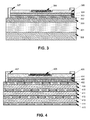
- FIG. 3 illustrates a cross-sectional view of an InGaAlN-based light-emitting device on a carbon-based substrate, which is obtained using a third fabrication process in accordance with one embodiment of the present invention.
- the light-emitting device is an LED.
- the light-emitting device in FIG. 3 is formed by wafer-bonding an InGaAlN-based multilayer structure onto a metal/carbon/metal composite substrate using a metal-bonding technique.
- the structure of FIG. 3 comprises the following components: a carbon-based layer 301 ; a metal layer 302 which is disposed between the InGaAlN-based multilayer structure and the carbon-based substrate; a P-type GaN layer 303 ; an InGaN/GaN MQW active layer 304 ; and an N-type GaN layer 305 .
- the structure of FIG. 3 further comprises a second Ohmic-contact electrode 306 , sidewall passivation material 307 , and metal layers 308 and 309 which are used to reinforce carbon-based layer 301 .
- FIG. 8A-8G illustrates a step-by-step process for fabricating the light-emitting device in FIG. 3 in accordance with one embodiment of the present invention.
- certain carbon-materials used to make carbon-based layer 301 can have very high thermal conductivity but relatively low strength.
- a metal/carbon/metal composite substrate structure can enhance the strength of the carbon-based substrate by depositing sufficiently thick metal layers on both sides of the carbon-based substrate.
- metal has high thermal conductivity, a metal substrate is typically difficult to dice. Consequently, one embodiment of the present invention can attain both high thermal conductivity devices and the flexibility in chip array separation.
- FIG. 6A illustrates the epitaxial substrate for fabricating the light-emitting device in FIG. 3 in accordance with one embodiment of the present invention.
- the epitaxial substrate used in fabricating the devices of FIG. 3 has substantially the same characteristics as the epitaxial substrates used in the first and second embodiments.
- FIG. 8A illustrates the cross-sectional view of the epitaxial substrate for fabricating the light-emitting device in FIG. 3 after depositing an Ohmic-contact layer 824 and a metal bonding layer 825 in accordance with one embodiment of the present invention.
- the epitaxial substrate as is shown in FIG. 8A has substantially the same characteristics as the epitaxial substrates after depositing the corresponding Ohmic-contact layers and metal bonding layers in the first and second embodiments.
- FIG. 8B illustrates the cross-sectional view of the metal/carbon/metal composite substrate after forming graphite infiltration layers 837 and 841 , metal reinforcement layers 835 and 838 , and a metal bonding layer 834 in accordance with one embodiment of the present invention.
- the metal/carbon/metal composite substrate comprises a carbon-based layer 836 , which has substantially the same characteristics as the corresponding carbon-based layers in the first and second embodiments.
- the carbon-based infiltration layers 837 and 841 have substantially the same characteristics as the corresponding infiltration layers in the first and second embodiments.
- metal reinforcement layers 835 and 838 are disposed directly above and underneath infiltration layers 837 and 841 , respectively, wherein these metal layers provide extra strength to carbon-based layer 836 .
- Each of the metal layers 835 and 838 can comprise a multilayer metal structure or a single metal structure. Additionally, they can be made of a single-element metal or an alloy. In one embodiment, each of the metal layers is greater than 1 ⁇ m.
- metal layers 835 and 838 are made of Ag.
- these metal layers can be made of Cu, Cu/W alloy, Cu/Mo alloy, or any other alloy that has a thermal conductivity greater than that of Si. It is important that metal layers 835 and 838 be protected by a conducting layer, and that this protective layer is resistant to Si-etchants. This protective layer can also be an insulator. If so, this protective layer needs to be removed after the subsequent Si-etching process.
- the metal/carbon/metal composite substrate also comprises a metal bonding layer 834 .
- metal bonding layer 834 have substantially the same characteristics as the corresponding metal bonding layer in the first and second embodiments.
- FIG. 8C illustrates the cross-sectional view of the epitaxial substrate in FIG. 8A and the metal/carbon/metal composite substrate in FIG. 8B after wafer bonding in accordance with one embodiment of the present invention.
- the combined substrates in FIG. 8C is subjected to heating and pressure over a specific period. Note that the bonding conditions and environment are substantially the same as the corresponding conditions and environments in the first and second embodiments.
- Si-etchant etches and removes original growth substrate 822 on the epitaxial substrate, and facilitates transferring InGaAlN multilayer structures 821 from the epitaxial substrate to the metal/carbon/metal composite substrate, as is shown in FIG. 8D .
- FIG. 8D illustrates the cross-sectional view of the light-emitting devices which are transferred on the metal/carbon/metal composite substrate by removing the epitaxial substrate in FIG. 8C .
- a sequence of wafer fabrication processes are performed to obtain the chip array as shown in FIG. 8E .
- These wafer fabrication processes are substantially the same as the corresponding wafer fabrication processes using to obtain the chip arrays in the first and second embodiments.
- FIG. 8E illustrates the cross-sectional view of the chip array formed on the metal/carbon/metal composite substrate after the sequence of wafer fabrication processes.
- FIG. 8F illustrates the process of dicing the wafer of FIG. 8E in accordance with one embodiment of the present invention.
- the process starts by creating dicing channels 839 and 840 on both the front-side and the backside of the metal/carbon/metal composite substrate using a combined photolithographic patterning and chemical etching technique.
- the wafer is separated along these dicing channels using a wafer-dicing machine, thereby obtaining single-unit light-emitting devices.
- FIG. 8G illustrates the cross-sectional view of the array of individual chips obtained from dicing the metal/carbon/metal composite substrate in FIG. 8F in accordance with one embodiment of the present invention.
- metal reinforcement layer 838 can be removed from carbon-based layer 801 .
- metal reinforcement layer 838 serves as a temporary structure that provides substrate reinforcement during the wafer fabrication process.
- FIG. 4 illustrates a cross-sectional view of an InGaAlN-based light-emitting device on a carbon-based substrate, which is obtained using a fourth fabrication process in accordance with one embodiment of the present invention.
- the light-emitting device is an LED.
- the light-emitting device in FIG. 4 is formed by wafer-bonding an InGaAlN-based multilayer structure onto a multilayer carbon/metal composite substrate using a metal-bonding technique.
- the wafer structure in FIG. 4 comprises the following components: a metal layer 402 which is disposed between the InGaAlN-based multilayer structure and the carbon-based substrate, a P-type GaN layer 403 , an InGaN/GaN MQW active layer 404 , and an N-type GaN layer 405 .
- the structure of FIG. 4 further comprises a second Ohmic-contact electrode 406 , sidewall passivation material 407 , multiple carbon-based layers 410 , 412 , and 414 , and multiple metal layers 409 , 411 , 413 , and 415 , which provide reinforcement to the carbon-based layers.
- the epitaxial substrate used in fabricating the devices of FIG. 4 has substantially the same characteristics as the epitaxial substrates used in the first, second, and third embodiments.
- the Ohmic-contact layers and metal bonding layers in FIG. 4 have substantially the same characteristics as the corresponding Ohmic-contact layers and corresponding metal bonding layers in the first, second, and third embodiments.
- the wafer structure in FIG. 4 is obtained as follows. First, a number of carbon-based layers are received, and carbon infiltration layers are deposited on both sides of each of the carbon-based layers. Metal bonding layers are then deposited on the infiltration layers on both sides of each of the carbon-based layers. Next, the multiple carbon-based layers comprising double-sided metal layers and the epitaxial substrate comprising the Ohmic-contact layer and the metal bonding layer are stacked and welded together. Finally, the chip array is fabricated using substantially the same wafer fabrication processes that are used in the first, second, and third embodiments.
- this embodiment of the present invention allows graphite cloth, carbon fiber cloth, and other laminated high-thermal-conductivity carbon-based materials to be used to prepare high thermal conductivity light emitting devices.
- the carbon-based substrate of this embodiment is formed by laminating and bonding multiple thin layers of carbon-based material together.
- the number of the thin layers can be equal to or greater than three.
- the thicknesses of metal layers 411 and 413 in this embodiment is no more than 10 ⁇ m.
- metal layers 409 and 415 can be thicker or thinner than 10 ⁇ m.
- a wafer dicing process substantially similar to the one used in the third embodiment can be applied. Specifically, dicing channels are etched in the wafer using a combined photolithographic patterning and chemical etching technique, which is followed by a wafer-scribing process to separate the chips along these dicing channels.
- the multilayer carbon/metal composite substrate of the current embodiment can be obtained by bonding multiple single carbon layers simultaneously with bonding the epitaxial substrate to the carbon-based substrate.
- the multilayer carbon/metal composite substrate can be obtained prior to wafer-bonding the epitaxial substrate to the carbon-based substrate.
- FIG. 5 illustrates a cross-sectional view of an InGaAlN-based light-emitting device on a carbon-based substrate, which is obtained using a fifth fabrication process in accordance with one embodiment of the present invention.
- the light-emitting device is an LED.
- the light-emitting device in FIG. 5 is formed by wafer-bonding an InGaAlN-based multilayer structure onto a metal/carbon/metal/carbon/metal composite substrate using a metal-bonding technique.
- the wafer structure in FIG. 5 comprises the following components: a metal layer 502 which is disposed between the InGaAlN-based multilayer structure and the carbon-based substrate; a P-type GaN layer 503 ; an InGaN/GaN MQW active layer 504 ; and an N-type GaN layer 505 .
- the structure of FIG. 5 further comprises a second Ohmic-contact electrode 506 , sidewall passivation material 507 , carbon-based layers 517 and 519 , and multiple metal layers 516 , 518 , and 520 , which provide reinforcement to the carbon-based layers.
- metal layer 518 is a thin layer with a thickness less than 20 ⁇ m.
- the epitaxial substrate used in fabricating the devices of FIG. 5 has substantially the same characteristics as the epitaxial substrates used in the first, second, third, and fourth embodiments.
- the Ohmic-contact layers and metal bonding layers in FIG. 5 have substantially the same characteristics as the corresponding Ohmic-contact layers and corresponding metal bonding layers in the first, second, third, and fourth embodiments.
- the wafer structure in FIG. 5 is obtained as follows. First, two carbon-based layers are received, and carbon-based infiltration layers are deposited on both sides of each of the carbon-based layers. Metal bonding layers are then deposited on the infiltration layers on both sides of each of the carbon-based layers. Next, the two carbon-based layers comprising double-sided metal layers and the epitaxial substrate comprising the Ohmic-contact layer and the metal bonding layer are stacked and welded together. The chip array is fabricated using substantially the same wafer fabrication processes that are used in the first, second, third, and fourth embodiments. Finally, the array of chips are separated using substantially the same wafer dicing techniques used in the first, second, third, and fourth embodiments.
- carbon-based layers 517 and 519 in FIG. 5 are made of natural graphite, pyrolytic graphite, or other carbon-based materials which have anisotropic thermal conduction characteristics
- the atomic-lattice planes of layers 517 and 519 can be placed perpendicular to the plane of the InGaAlN-based multilayer structure.
- carbon-based layers 517 and 519 can be arranged such that their atomic-lattice planes are kept at a specific angle with respect to each other. In a preferred embodiment, this angle is 90°.
- the metal/carbon/metal/carbon/metal composite substrate of the current embodiment can be obtained by bonding two single carbon layers at the same time of bonding the epitaxial substrate to the carbon-based substrate.
- the metal/carbon/metal/carbon/metal composite substrate can be obtained prior to wafer-bonding the epitaxial substrate to the carbon-based substrate.
- a wafer dicing process substantially similar to the one used in the third embodiment can be applied. Specifically, dicing channels are etched in the wafer using a combined photolithographic patterning and chemical etching technique, which is followed by a wafer-scribing process to separate the chips along these dicing channels.
- Metal layer 518 can be a thin layer with a thickness less than 10 ⁇ m, or a thick layer with a thickness greater than 10 ⁇ m. If metal layer 518 is thicker than 10 ⁇ m, dicing channels can be first created in the carbon-based layers on both sides of metal layer 518 . Next, the sections of metal layer 518 in the gaps between the chip arrays are etched away using a chemical-etching process, which causes the array of chips to separate.
Abstract
Description
-
- (1) Removing the InGaAlN-based material and metal which have been deposited in
channel 623 ofgrowth substrate 622. The removing techniques can include ultrasonic cleaning, compressed air blowing, or mechanical scrubbing. - (2) Removing a specific thickness of N-type layer 105 (see
FIG. 1 ) within a region inside N-type layer 105, where N-type layer electrode metal is to be deposited. A pit structure is effectively etched into N-type layer 105, wherein the pit depth is not more than the thickness of N-type layer 105. The pit can be fabricated using a reactive ion etching (RIE) technique or a wet-etching technique. If an RIE technique is used, the reactive gas can include a chlorine-based gas or any other gas suitable for etching GaN. If a wet-etching technique is used, the etchant can include phosphoric acid, NaOH, or KOH. The wet-etching process can also be assisted by ultraviolet light illumination. Note that regions of N-type layer 105 which are not to be etched can be protected with a mask material, which can include photoresist, metal, or a combination of photoresist and metal. - (3) Forming N-type layer Ohmic-
contact electrode 106 in the etched pit of N-type layer 105 and additionally removing low-quality boundary regions ofInGaAlN multilayer structure 621 which are affected by the boundary effect due to the existence ofchannels 623 ingrowth substrate 622. The boundary removal technique can include any above-mentioned dry etching techniques, wet-etching techniques, or a combination of both. Note that N-type layer Ohmic-contact electrode 106 can be made of a Au/Germanium (Ge)/Ni alloy, a Au/Si alloy, TiN, Ti/Aluminum (Al) alloy, or a combination of two or more of the Au/Ge/Ni, Au/Si, TiN, and Ti/Al alloys. In one embodiment of the present invention, a cover layer is deposited on top of Ohmic-contact electrode 106 to facilitate welding lead wires on Ohmic-contact electrode 106. This cover layer can include a Ti/Au double-layer or Ni/Au double-layer. - (4) Removing excessive metal between chips in the chip array in
FIG. 6A . This allows exposing spaces between chips for mechanical dicing of the chips, exposing carbon-based layer, and fabricatingpassivation layer 107/607 on the chip sidewalls. Note that if the graphite infiltration layers thickness is less than 2 μm, the graphite infiltration layer between the gaps of chips array can be left alone. Thesidewall passivation material 107/607 can be inorganic insulating materials, such as SiO2, Al2O3, or Si3N4. Passivation material 107/607 can also be organic insulating materials such as PI, and any other common passivation materials using in electronic devices.
- (1) Removing the InGaAlN-based material and metal which have been deposited in
Claims (20)
Applications Claiming Priority (3)
| Application Number | Priority Date | Filing Date | Title |
|---|---|---|---|
| CN200710107760.2 | 2007-04-29 | ||
| CN2007101077602A CN101295758B (en) | 2007-04-29 | 2007-04-29 | Indium gallium aluminum nitrogen illuminating device containing carbon based underlay and its production method |
| CN200710107760 | 2007-04-29 |
Publications (2)
| Publication Number | Publication Date |
|---|---|
| US20080265265A1 US20080265265A1 (en) | 2008-10-30 |
| US7741632B2 true US7741632B2 (en) | 2010-06-22 |
Family
ID=39885887
Family Applications (1)
| Application Number | Title | Priority Date | Filing Date |
|---|---|---|---|
| US11/778,213 Expired - Fee Related US7741632B2 (en) | 2007-04-29 | 2007-07-16 | InGaAIN light-emitting device containing carbon-based substrate and method for making the same |
Country Status (4)
| Country | Link |
|---|---|
| US (1) | US7741632B2 (en) |
| EP (1) | EP2171771A4 (en) |
| CN (1) | CN101295758B (en) |
| WO (1) | WO2008134929A1 (en) |
Cited By (8)
| Publication number | Priority date | Publication date | Assignee | Title |
|---|---|---|---|---|
| US20100051965A1 (en) * | 2008-08-29 | 2010-03-04 | Chen-Hua Yu | Carbon-Containing Semiconductor Substrate |
| US20110001120A1 (en) * | 2008-03-25 | 2011-01-06 | Lattice Power (Jiangxi) Corporation | Semiconductor light-emitting device with double-sided passivation |
| US20110175125A1 (en) * | 2010-01-15 | 2011-07-21 | Bae Jung Hyeok | Light emitting device, light emitting device package, and lighting system |
| US20130026499A1 (en) * | 2011-07-26 | 2013-01-31 | Micron Technology, Inc. | Wafer-level packaging for solid-state transducers and associated systems and methods |
| US20140011345A1 (en) * | 2012-06-14 | 2014-01-09 | Palo Alto Research Center Incorporated | Method of growing epitaxial layers on a substrate |
| US9196810B2 (en) | 2011-08-25 | 2015-11-24 | Micron Technology, Inc. | Vertical solid-state transducers having backside terminals and associated systems and methods |
| US9224633B2 (en) | 2010-09-30 | 2015-12-29 | Infineon Technologies Ag | Method for manufacturing a composite wafer having a graphite core, and composite wafer having a graphite core |
| US9252045B2 (en) | 2010-09-30 | 2016-02-02 | Infineon Technologies Ag | Method for manufacturing a composite wafer having a graphite core |
Families Citing this family (27)
| Publication number | Priority date | Publication date | Assignee | Title |
|---|---|---|---|---|
| EP2201613A1 (en) * | 2007-08-31 | 2010-06-30 | Lattice Power (Jiangxi) Corporation | Method for fabricating a low-resistivity ohmic contact to a p-type iii-v nitride semiconductor material at low temperature |
| KR20090072980A (en) * | 2007-12-28 | 2009-07-02 | 서울옵토디바이스주식회사 | Light emitting diode and method of fabricating the same |
| US7569432B1 (en) * | 2008-01-14 | 2009-08-04 | Chang Gung University | Method of manufacturing an LED |
| CN104538507B (en) * | 2008-06-02 | 2017-08-15 | Lg伊诺特有限公司 | Method for preparing semiconductor light-emitting apparatus |
| WO2010020069A1 (en) * | 2008-08-19 | 2010-02-25 | Lattice Power (Jiangxi) Corporation | METHOD FOR FABRICATING InGaAlN LIGHT-EMITTING DIODES WITH A METAL SUBSTRATE |
| TWI470823B (en) * | 2009-02-11 | 2015-01-21 | Epistar Corp | Light-emitting device and manufacturing method thereof |
| CN102414837B (en) * | 2009-02-27 | 2016-04-20 | 奥塔装置公司 | For depositing the tiling substrate with extension stripping process |
| CN101710567A (en) * | 2009-11-27 | 2010-05-19 | 晶能光电(江西)有限公司 | Gallium nitride-based semiconductor device with composite carbon-based substrate and manufacturing method thereof |
| KR101172950B1 (en) | 2009-12-02 | 2012-08-10 | 정경화 | Graphite substrate for light emitting diode and light emitting diode using the same |
| FR2967813B1 (en) * | 2010-11-18 | 2013-10-04 | Soitec Silicon On Insulator | METHOD FOR PRODUCING A BENTALLIC METAL LAYER STRUCTURE |
| CN102610706B (en) * | 2011-01-24 | 2016-03-02 | 晶能光电(江西)有限公司 | Stress control method in indium-gallium-aluminum-nitrogen base luminescent device manufacture process |
| TW201301570A (en) * | 2011-06-28 | 2013-01-01 | Aceplux Optotech Inc | Multi-color light emitting diode and manufacturing method thereof |
| CN103066026B (en) * | 2011-10-21 | 2015-10-21 | 稳懋半导体股份有限公司 | High breaking strength semiconductor transistor elements structure-improved and manufacture method thereof |
| TWI480941B (en) * | 2011-10-21 | 2015-04-11 | Win Semiconductors Corp | A structure of semiconductor chips with enhanced die strength and a fabrication method thereof |
| US8835283B2 (en) * | 2011-10-21 | 2014-09-16 | Win Semiconductors Corp. | Fabrication method for producing semiconductor chips with enhanced die strength |
| TWI528578B (en) * | 2012-03-28 | 2016-04-01 | 鴻海精密工業股份有限公司 | Method for manufacturing light emitting diode |
| CN103035518A (en) * | 2012-05-09 | 2013-04-10 | 上海华虹Nec电子有限公司 | Manufacture method of insulated gate bipolar transistor wafer |
| US9196688B2 (en) * | 2013-03-05 | 2015-11-24 | Infineon Technologies Americas Corp. | Delamination and crack prevention in III-nitride wafers |
| CN105990165B (en) * | 2015-02-02 | 2019-01-22 | 中芯国际集成电路制造(上海)有限公司 | Semiconductor structure and forming method thereof |
| CN105489717A (en) * | 2016-01-11 | 2016-04-13 | 西安交通大学 | Fabrication process for vertically structured light emitting diode (LED) chip |
| CN105762263A (en) * | 2016-04-01 | 2016-07-13 | 陕西新光源科技有限责任公司 | Method for preparing bonding substrate for LED chip |
| US9905466B2 (en) * | 2016-06-28 | 2018-02-27 | Taiwan Semiconductor Manufacturing Company, Ltd. | Wafer partitioning method and device formed |
| DE102018111324A1 (en) * | 2018-05-11 | 2019-11-14 | Osram Opto Semiconductors Gmbh | Optoelectronic semiconductor chip |
| WO2020019326A1 (en) * | 2018-07-27 | 2020-01-30 | 天津三安光电有限公司 | Semiconductor luminous element |
| CN111769103B (en) * | 2020-06-29 | 2023-05-09 | 南昌大学 | Preparation method of multicolor Micro LED light-emitting module |
| US11670567B2 (en) * | 2020-07-09 | 2023-06-06 | United Microelectronics Corp. | Semiconductor structure and method of wafer bonding |
| WO2024040513A1 (en) * | 2022-08-25 | 2024-02-29 | Innoscience (Zhuhai) Technology Co., Ltd. | Semiconductor device and method for manufacturing the same |
Citations (9)
| Publication number | Priority date | Publication date | Assignee | Title |
|---|---|---|---|---|
| US5389799A (en) | 1992-06-12 | 1995-02-14 | Kabushiki Kaisha Toshiba | Semiconductor device |
| US20020110282A1 (en) | 2001-02-09 | 2002-08-15 | Walter Kraft | Local change of an image sharpness of photographic images with masks |
| US6521917B1 (en) | 1999-03-26 | 2003-02-18 | Matsushita Electric Industrial Co., Ltd. | Semiconductor structures using a group III-nitride quaternary material system with reduced phase separation |
| US20040241447A1 (en) * | 2003-05-16 | 2004-12-02 | Hitachi Metals, Ltd. | Composite material having high thermal conductivity and low thermal expansion coefficient, and heat-dissipating substrate, and their production methods |
| US20050006664A1 (en) | 2001-03-27 | 2005-01-13 | Matsushita Electric Industrial Co., Ltd. | Semisonductor device |
| US6903364B1 (en) | 1999-03-26 | 2005-06-07 | Matsushita Electric Industrial Co., Ltd. | Semiconductor structures using a group III-nitride material system with reduced phase separation and method of fabrication |
| US20060255341A1 (en) * | 2005-04-21 | 2006-11-16 | Aonex Technologies, Inc. | Bonded intermediate substrate and method of making same |
| JP2007035898A (en) * | 2005-07-27 | 2007-02-08 | Nippon Telegr & Teleph Corp <Ntt> | Uwb transmitter |
| US20080157090A1 (en) * | 2006-12-28 | 2008-07-03 | Darren Brent Thomson | Transplanted epitaxial regrowth for fabricating large area substrates for electronic devices |
Family Cites Families (6)
| Publication number | Priority date | Publication date | Assignee | Title |
|---|---|---|---|---|
| JP3260001B2 (en) * | 1992-06-12 | 2002-02-25 | 株式会社東芝 | Semiconductor element |
| JP3760478B2 (en) * | 1995-05-18 | 2006-03-29 | 昭和電工株式会社 | Method for producing group III-V compound semiconductor device |
| TWI283031B (en) * | 2002-03-25 | 2007-06-21 | Epistar Corp | Method for integrating compound semiconductor with substrate of high thermal conductivity |
| KR100483049B1 (en) * | 2003-06-03 | 2005-04-15 | 삼성전기주식회사 | A METHOD OF PRODUCING VERTICAL GaN LIGHT EMITTING DIODES |
| CN100372137C (en) * | 2005-05-27 | 2008-02-27 | 晶能光电(江西)有限公司 | Indium gallium aluminum nitrogen luminous device with up-down cathode strucure and manufacturing method thereof |
| CN100474642C (en) * | 2005-10-27 | 2009-04-01 | 晶能光电(江西)有限公司 | Indium gallium aluminium nitrogen semi-conductor luminous element containing metallic chromium substrate and manufacturing method thereof |
-
2007
- 2007-04-29 CN CN2007101077602A patent/CN101295758B/en active Active
- 2007-07-16 US US11/778,213 patent/US7741632B2/en not_active Expired - Fee Related
-
2008
- 2008-04-28 WO PCT/CN2008/000856 patent/WO2008134929A1/en active Application Filing
- 2008-04-28 EP EP08748415.0A patent/EP2171771A4/en not_active Withdrawn
Patent Citations (10)
| Publication number | Priority date | Publication date | Assignee | Title |
|---|---|---|---|---|
| US5389799A (en) | 1992-06-12 | 1995-02-14 | Kabushiki Kaisha Toshiba | Semiconductor device |
| US6521917B1 (en) | 1999-03-26 | 2003-02-18 | Matsushita Electric Industrial Co., Ltd. | Semiconductor structures using a group III-nitride quaternary material system with reduced phase separation |
| US6903364B1 (en) | 1999-03-26 | 2005-06-07 | Matsushita Electric Industrial Co., Ltd. | Semiconductor structures using a group III-nitride material system with reduced phase separation and method of fabrication |
| US20050161698A1 (en) | 1999-03-26 | 2005-07-28 | Matsushita Electric Industrial Co., Ltd. | Semiconductor structures using a group III-nitride material system with reduced phase separation and method of fabrication |
| US20020110282A1 (en) | 2001-02-09 | 2002-08-15 | Walter Kraft | Local change of an image sharpness of photographic images with masks |
| US20050006664A1 (en) | 2001-03-27 | 2005-01-13 | Matsushita Electric Industrial Co., Ltd. | Semisonductor device |
| US20040241447A1 (en) * | 2003-05-16 | 2004-12-02 | Hitachi Metals, Ltd. | Composite material having high thermal conductivity and low thermal expansion coefficient, and heat-dissipating substrate, and their production methods |
| US20060255341A1 (en) * | 2005-04-21 | 2006-11-16 | Aonex Technologies, Inc. | Bonded intermediate substrate and method of making same |
| JP2007035898A (en) * | 2005-07-27 | 2007-02-08 | Nippon Telegr & Teleph Corp <Ntt> | Uwb transmitter |
| US20080157090A1 (en) * | 2006-12-28 | 2008-07-03 | Darren Brent Thomson | Transplanted epitaxial regrowth for fabricating large area substrates for electronic devices |
Cited By (23)
| Publication number | Priority date | Publication date | Assignee | Title |
|---|---|---|---|---|
| US20110001120A1 (en) * | 2008-03-25 | 2011-01-06 | Lattice Power (Jiangxi) Corporation | Semiconductor light-emitting device with double-sided passivation |
| US7943942B2 (en) * | 2008-03-25 | 2011-05-17 | Lattice Power (Jiangxi) Corporation | Semiconductor light-emitting device with double-sided passivation |
| US8148732B2 (en) * | 2008-08-29 | 2012-04-03 | Taiwan Semiconductor Manufacturing, Co., Ltd. | Carbon-containing semiconductor substrate |
| US20100051965A1 (en) * | 2008-08-29 | 2010-03-04 | Chen-Hua Yu | Carbon-Containing Semiconductor Substrate |
| US9076947B2 (en) | 2010-01-15 | 2015-07-07 | Lg Innotek Co., Ltd. | Light emitting device, light emitting device package, and lighting system |
| US20110175125A1 (en) * | 2010-01-15 | 2011-07-21 | Bae Jung Hyeok | Light emitting device, light emitting device package, and lighting system |
| US8686453B2 (en) | 2010-01-15 | 2014-04-01 | LG Innotek Co.,, Ltd. | Light emitting device, light emitting device package, and lighting system |
| US9576844B2 (en) | 2010-09-30 | 2017-02-21 | Infineon Technologies Ag | Method for manufacturing a composite wafer having a graphite core, and composite wafer having a graphite core |
| US9252045B2 (en) | 2010-09-30 | 2016-02-02 | Infineon Technologies Ag | Method for manufacturing a composite wafer having a graphite core |
| US9224633B2 (en) | 2010-09-30 | 2015-12-29 | Infineon Technologies Ag | Method for manufacturing a composite wafer having a graphite core, and composite wafer having a graphite core |
| US20130026499A1 (en) * | 2011-07-26 | 2013-01-31 | Micron Technology, Inc. | Wafer-level packaging for solid-state transducers and associated systems and methods |
| US8952395B2 (en) * | 2011-07-26 | 2015-02-10 | Micron Technology, Inc. | Wafer-level solid state transducer packaging transducers including separators and associated systems and methods |
| US10008647B2 (en) | 2011-07-26 | 2018-06-26 | Micron Technology, Inc. | Wafer-level solid state transducer packaging transducers including separators and associated systems and methods |
| US20180309033A1 (en) * | 2011-07-26 | 2018-10-25 | Micron Technology, Inc. | Wafer-level solid state transducer packaging transducers including separators and associated systems and methods |
| US11094860B2 (en) * | 2011-07-26 | 2021-08-17 | Micron Technology, Inc. | Wafer-level solid state transducer packaging transducers including separators and associated systems and methods |
| US11843082B2 (en) | 2011-07-26 | 2023-12-12 | Micron Technology, Inc. | Wafer-level solid state transducer packaging transducers including separators and associated systems and methods |
| US9196810B2 (en) | 2011-08-25 | 2015-11-24 | Micron Technology, Inc. | Vertical solid-state transducers having backside terminals and associated systems and methods |
| US9601675B2 (en) | 2011-08-25 | 2017-03-21 | Micron Technology, Inc. | Vertical solid-state transducers having backside terminals and associated systems and methods |
| US10333039B2 (en) | 2011-08-25 | 2019-06-25 | Micron Technology, Inc. | Vertical solid-state transducers having backside terminals and associated systems and methods |
| US10886445B2 (en) | 2011-08-25 | 2021-01-05 | Micron Technology, Inc. | Vertical solid-state transducers having backside terminals and associated systems and methods |
| US11784294B2 (en) | 2011-08-25 | 2023-10-10 | Micron Technology, Inc. | Vertical solid-state transducers having backside terminals and associated systems and methods |
| US8822314B2 (en) * | 2012-06-14 | 2014-09-02 | Palo Alto Research Center Incorporated | Method of growing epitaxial layers on a substrate |
| US20140011345A1 (en) * | 2012-06-14 | 2014-01-09 | Palo Alto Research Center Incorporated | Method of growing epitaxial layers on a substrate |
Also Published As
| Publication number | Publication date |
|---|---|
| CN101295758B (en) | 2013-03-06 |
| EP2171771A1 (en) | 2010-04-07 |
| CN101295758A (en) | 2008-10-29 |
| WO2008134929A1 (en) | 2008-11-13 |
| US20080265265A1 (en) | 2008-10-30 |
| EP2171771A4 (en) | 2015-12-02 |
Similar Documents
| Publication | Publication Date | Title |
|---|---|---|
| US7741632B2 (en) | InGaAIN light-emitting device containing carbon-based substrate and method for making the same | |
| EP2262012B1 (en) | Light-emitting diode and a method of manufacturing thereof | |
| JP5305364B2 (en) | Method for manufacturing vertical structure semiconductor light emitting device | |
| US7268372B2 (en) | Vertical GaN light emitting diode and method for manufacturing the same | |
| US8338202B2 (en) | Method for manufacturing semiconductor device using separable support body | |
| EP2261949B1 (en) | LED having vertical structure | |
| TWI431798B (en) | Light emitting diode with conducting metal substrate | |
| JP5693553B2 (en) | Thin film semiconductor chip | |
| US7943942B2 (en) | Semiconductor light-emitting device with double-sided passivation | |
| KR101198758B1 (en) | Vertical structured semiconductor light emitting device and method for producing thereof | |
| JP2008543032A (en) | InGaAlN light emitting device and manufacturing method thereof | |
| US20130307123A1 (en) | Semiconductor device having plurality of bonding layers and method of manufacturing the same | |
| US20110140081A1 (en) | Method for fabricating semiconductor light-emitting device with double-sided passivation | |
| KR100999548B1 (en) | A supporting substrate for manufacturing vertical structured semiconductor light emitting device, method of manufacturing the semiconductor light emitting device using the supporting substrate and vertical structured semiconductor light emitting devices | |
| JP2010225852A (en) | Semiconductor element, and method of manufacturing the same | |
| KR101203137B1 (en) | GaN compound semiconductor light emitting element and method of manufacturing the same | |
| JP2008016629A (en) | Manufacturing method of group iii nitride light emitting diode element | |
| KR101499954B1 (en) | fabrication of vertical structured light emitting diodes using group 3 nitride-based semiconductors and its related methods | |
| KR20090105462A (en) | Vertical structured group 3 nitride-based light emitting diode and its fabrication methods | |
| KR101480551B1 (en) | vertical structured group 3 nitride-based light emitting diode and its fabrication methods | |
| KR101510382B1 (en) | fabrication of vertical structured light emitting diodes using group 3 nitride-based semiconductors and its related methods | |
| KR101115571B1 (en) | GaN compound semiconductor light emitting element |
Legal Events
| Date | Code | Title | Description |
|---|---|---|---|
| AS | Assignment |
Owner name: LATTICE POWER (JIANGXI) CORPORATION, CHINA Free format text: ASSIGNMENT OF ASSIGNORS INTEREST;ASSIGNORS:XIONG, CHUANBING;JIANG, FENGYI;WANG, LI;AND OTHERS;REEL/FRAME:019627/0649 Effective date: 20070702 Owner name: LATTICE POWER (JIANGXI) CORPORATION,CHINA Free format text: ASSIGNMENT OF ASSIGNORS INTEREST;ASSIGNORS:XIONG, CHUANBING;JIANG, FENGYI;WANG, LI;AND OTHERS;REEL/FRAME:019627/0649 Effective date: 20070702 |
|
| STCF | Information on status: patent grant |
Free format text: PATENTED CASE |
|
| FPAY | Fee payment |
Year of fee payment: 4 |
|
| FPAY | Fee payment |
Year of fee payment: 8 |
|
| FEPP | Fee payment procedure |
Free format text: MAINTENANCE FEE REMINDER MAILED (ORIGINAL EVENT CODE: REM.); ENTITY STATUS OF PATENT OWNER: SMALL ENTITY |
|
| LAPS | Lapse for failure to pay maintenance fees |
Free format text: PATENT EXPIRED FOR FAILURE TO PAY MAINTENANCE FEES (ORIGINAL EVENT CODE: EXP.); ENTITY STATUS OF PATENT OWNER: SMALL ENTITY |
|
| STCH | Information on status: patent discontinuation |
Free format text: PATENT EXPIRED DUE TO NONPAYMENT OF MAINTENANCE FEES UNDER 37 CFR 1.362 |
|
| FP | Lapsed due to failure to pay maintenance fee |
Effective date: 20220622 |