US7736990B2 - Semiconductor device and manufacturing method for the same - Google Patents
Semiconductor device and manufacturing method for the same Download PDFInfo
- Publication number
- US7736990B2 US7736990B2 US12/270,659 US27065908A US7736990B2 US 7736990 B2 US7736990 B2 US 7736990B2 US 27065908 A US27065908 A US 27065908A US 7736990 B2 US7736990 B2 US 7736990B2
- Authority
- US
- United States
- Prior art keywords
- insulating film
- removal step
- semiconductor device
- film
- trench region
- Prior art date
- Legal status (The legal status is an assumption and is not a legal conclusion. Google has not performed a legal analysis and makes no representation as to the accuracy of the status listed.)
- Active
Links
- 239000004065 semiconductor Substances 0.000 title claims abstract description 65
- 238000004519 manufacturing process Methods 0.000 title claims abstract description 17
- 238000000034 method Methods 0.000 claims abstract description 66
- 239000000758 substrate Substances 0.000 claims abstract description 45
- 238000005498 polishing Methods 0.000 claims abstract description 32
- 239000000126 substance Substances 0.000 claims abstract description 9
- 239000002245 particle Substances 0.000 claims description 16
- VYPSYNLAJGMNEJ-UHFFFAOYSA-N Silicium dioxide Chemical compound O=[Si]=O VYPSYNLAJGMNEJ-UHFFFAOYSA-N 0.000 claims description 11
- 229910052814 silicon oxide Inorganic materials 0.000 claims description 11
- 239000000203 mixture Substances 0.000 claims description 7
- 239000002002 slurry Substances 0.000 claims description 6
- 238000005268 plasma chemical vapour deposition Methods 0.000 claims description 5
- 238000002955 isolation Methods 0.000 description 16
- 150000004767 nitrides Chemical class 0.000 description 11
- 238000010586 diagram Methods 0.000 description 9
- XUIMIQQOPSSXEZ-UHFFFAOYSA-N Silicon Chemical compound [Si] XUIMIQQOPSSXEZ-UHFFFAOYSA-N 0.000 description 8
- 229910052710 silicon Inorganic materials 0.000 description 8
- 239000010703 silicon Substances 0.000 description 8
- KRHYYFGTRYWZRS-UHFFFAOYSA-N Fluorane Chemical compound F KRHYYFGTRYWZRS-UHFFFAOYSA-N 0.000 description 7
- 239000004094 surface-active agent Substances 0.000 description 7
- 229910000040 hydrogen fluoride Inorganic materials 0.000 description 6
- 230000003647 oxidation Effects 0.000 description 6
- 238000007254 oxidation reaction Methods 0.000 description 6
- XLYOFNOQVPJJNP-UHFFFAOYSA-N water Substances O XLYOFNOQVPJJNP-UHFFFAOYSA-N 0.000 description 5
- 230000015572 biosynthetic process Effects 0.000 description 4
- 238000005229 chemical vapour deposition Methods 0.000 description 4
- 238000005530 etching Methods 0.000 description 4
- 239000010410 layer Substances 0.000 description 4
- 239000002904 solvent Substances 0.000 description 4
- 238000001312 dry etching Methods 0.000 description 3
- 230000005684 electric field Effects 0.000 description 3
- 239000012535 impurity Substances 0.000 description 3
- 239000011229 interlayer Substances 0.000 description 3
- 239000007788 liquid Substances 0.000 description 3
- 238000001020 plasma etching Methods 0.000 description 3
- 238000001039 wet etching Methods 0.000 description 3
- 241000293849 Cordylanthus Species 0.000 description 2
- 239000003990 capacitor Substances 0.000 description 2
- 229910000420 cerium oxide Inorganic materials 0.000 description 2
- 239000013078 crystal Substances 0.000 description 2
- 238000000151 deposition Methods 0.000 description 2
- 230000008021 deposition Effects 0.000 description 2
- 239000006185 dispersion Substances 0.000 description 2
- 239000000463 material Substances 0.000 description 2
- BMMGVYCKOGBVEV-UHFFFAOYSA-N oxo(oxoceriooxy)cerium Chemical compound [Ce]=O.O=[Ce]=O BMMGVYCKOGBVEV-UHFFFAOYSA-N 0.000 description 2
- 229920002120 photoresistant polymer Polymers 0.000 description 2
- 238000006748 scratching Methods 0.000 description 2
- 230000002393 scratching effect Effects 0.000 description 2
- 238000005406 washing Methods 0.000 description 2
- 229910000577 Silicon-germanium Inorganic materials 0.000 description 1
- LEVVHYCKPQWKOP-UHFFFAOYSA-N [Si].[Ge] Chemical compound [Si].[Ge] LEVVHYCKPQWKOP-UHFFFAOYSA-N 0.000 description 1
- 230000002411 adverse Effects 0.000 description 1
- XAGFODPZIPBFFR-UHFFFAOYSA-N aluminium Chemical compound [Al] XAGFODPZIPBFFR-UHFFFAOYSA-N 0.000 description 1
- 229910052782 aluminium Inorganic materials 0.000 description 1
- 239000005380 borophosphosilicate glass Substances 0.000 description 1
- 150000001875 compounds Chemical class 0.000 description 1
- 238000007796 conventional method Methods 0.000 description 1
- 230000006866 deterioration Effects 0.000 description 1
- 238000011161 development Methods 0.000 description 1
- 230000000694 effects Effects 0.000 description 1
- 230000007613 environmental effect Effects 0.000 description 1
- 229910052732 germanium Inorganic materials 0.000 description 1
- GNPVGFCGXDBREM-UHFFFAOYSA-N germanium atom Chemical compound [Ge] GNPVGFCGXDBREM-UHFFFAOYSA-N 0.000 description 1
- 238000005468 ion implantation Methods 0.000 description 1
- 150000002500 ions Chemical class 0.000 description 1
- 230000007257 malfunction Effects 0.000 description 1
- 238000012986 modification Methods 0.000 description 1
- 230000004048 modification Effects 0.000 description 1
- 238000012544 monitoring process Methods 0.000 description 1
- 230000001590 oxidative effect Effects 0.000 description 1
- 229910021420 polycrystalline silicon Inorganic materials 0.000 description 1
- 229920005591 polysilicon Polymers 0.000 description 1
- 238000012545 processing Methods 0.000 description 1
- 238000003672 processing method Methods 0.000 description 1
- 239000005368 silicate glass Substances 0.000 description 1
- 241000894007 species Species 0.000 description 1
Images


Classifications
-
- H—ELECTRICITY
- H01—ELECTRIC ELEMENTS
- H01L—SEMICONDUCTOR DEVICES NOT COVERED BY CLASS H10
- H01L21/00—Processes or apparatus adapted for the manufacture or treatment of semiconductor or solid state devices or of parts thereof
- H01L21/70—Manufacture or treatment of devices consisting of a plurality of solid state components formed in or on a common substrate or of parts thereof; Manufacture of integrated circuit devices or of parts thereof
- H01L21/71—Manufacture of specific parts of devices defined in group H01L21/70
- H01L21/76—Making of isolation regions between components
- H01L21/762—Dielectric regions, e.g. EPIC dielectric isolation, LOCOS; Trench refilling techniques, SOI technology, use of channel stoppers
- H01L21/76224—Dielectric regions, e.g. EPIC dielectric isolation, LOCOS; Trench refilling techniques, SOI technology, use of channel stoppers using trench refilling with dielectric materials
- H01L21/76232—Dielectric regions, e.g. EPIC dielectric isolation, LOCOS; Trench refilling techniques, SOI technology, use of channel stoppers using trench refilling with dielectric materials of trenches having a shape other than rectangular or V-shape, e.g. rounded corners, oblique or rounded trench walls
-
- H—ELECTRICITY
- H01—ELECTRIC ELEMENTS
- H01L—SEMICONDUCTOR DEVICES NOT COVERED BY CLASS H10
- H01L21/00—Processes or apparatus adapted for the manufacture or treatment of semiconductor or solid state devices or of parts thereof
- H01L21/02—Manufacture or treatment of semiconductor devices or of parts thereof
- H01L21/04—Manufacture or treatment of semiconductor devices or of parts thereof the devices having at least one potential-jump barrier or surface barrier, e.g. PN junction, depletion layer or carrier concentration layer
- H01L21/18—Manufacture or treatment of semiconductor devices or of parts thereof the devices having at least one potential-jump barrier or surface barrier, e.g. PN junction, depletion layer or carrier concentration layer the devices having semiconductor bodies comprising elements of Group IV of the Periodic System or AIIIBV compounds with or without impurities, e.g. doping materials
- H01L21/30—Treatment of semiconductor bodies using processes or apparatus not provided for in groups H01L21/20 - H01L21/26
- H01L21/31—Treatment of semiconductor bodies using processes or apparatus not provided for in groups H01L21/20 - H01L21/26 to form insulating layers thereon, e.g. for masking or by using photolithographic techniques; After treatment of these layers; Selection of materials for these layers
- H01L21/3105—After-treatment
- H01L21/31051—Planarisation of the insulating layers
- H01L21/31053—Planarisation of the insulating layers involving a dielectric removal step
-
- H—ELECTRICITY
- H01—ELECTRIC ELEMENTS
- H01L—SEMICONDUCTOR DEVICES NOT COVERED BY CLASS H10
- H01L21/00—Processes or apparatus adapted for the manufacture or treatment of semiconductor or solid state devices or of parts thereof
- H01L21/70—Manufacture or treatment of devices consisting of a plurality of solid state components formed in or on a common substrate or of parts thereof; Manufacture of integrated circuit devices or of parts thereof
- H01L21/77—Manufacture or treatment of devices consisting of a plurality of solid state components or integrated circuits formed in, or on, a common substrate
- H01L21/78—Manufacture or treatment of devices consisting of a plurality of solid state components or integrated circuits formed in, or on, a common substrate with subsequent division of the substrate into plural individual devices
- H01L21/82—Manufacture or treatment of devices consisting of a plurality of solid state components or integrated circuits formed in, or on, a common substrate with subsequent division of the substrate into plural individual devices to produce devices, e.g. integrated circuits, each consisting of a plurality of components
- H01L21/822—Manufacture or treatment of devices consisting of a plurality of solid state components or integrated circuits formed in, or on, a common substrate with subsequent division of the substrate into plural individual devices to produce devices, e.g. integrated circuits, each consisting of a plurality of components the substrate being a semiconductor, using silicon technology
- H01L21/8232—Field-effect technology
- H01L21/8234—MIS technology, i.e. integration processes of field effect transistors of the conductor-insulator-semiconductor type
- H01L21/823481—MIS technology, i.e. integration processes of field effect transistors of the conductor-insulator-semiconductor type isolation region manufacturing related aspects, e.g. to avoid interaction of isolation region with adjacent structure
Definitions
- the present invention relates to a semiconductor device and a method for manufacturing the same.
- the present invention relates to a method for manufacturing a semiconductor device which is appropriate for shallow trench isolation (STI) processes used to electrically isolate a great number of elements, as well as a semiconductor device obtained in accordance with this method.
- STI shallow trench isolation
- semiconductor devices have a configuration where a great number of cells made up of unit elements (for example, several thousand to several hundred million), such as transistors and capacitors, are integrated within an area restricted in accordance with the capacity of the semiconductor device. It is necessary for these unit elements to be electrically isolated (insulated) from each other so that they operate independently.
- unit elements for example, several thousand to several hundred million
- LOCOS local oxidation of silicon
- trench isolation methods in which a semiconductor substrate is etched in the vertical direction so that trench regions are formed, and then the trench regions are embedded with an insulating film, are widely known.
- trench regions include not only regions in a plane but also regions which spread in the direction of the depth.
- the LOCOS methods are simple and have fewer problems caused by stress from the oxide film, because the semiconductor substrate is thermally oxidized using a nitride film as a mask. Therefore, the LOCOS methods have an advantage, such that the quality of the obtained oxide film is excellent.
- the trench isolation methods are methods in which a dry etching technology, such as reactive ion etching (RIE) or plasma etching is used to form narrow and deep trench regions, which are then embedded with an insulating film.
- RIE reactive ion etching
- the trench regions formed on the semiconductor substrate are embedded with an insulating film, and therefore, no bird's beaks are formed.
- the surface of the insulating film with which the trench regions are embedded is flattened, and therefore, the area occupied by the element isolation regions becomes small.
- the trench isolation methods have an advantage, such that active regions (regions where unit elements are formed) can be secured as much as possible.
- the junction leak current can be reduced in comparison with the LOCOS methods.
- a trench isolation method is shown in, for example, Japanese Unexamined Patent Publication 2002-252279.
- FIG. 1 is a schematic cross sectional diagram showing the semiconductor device in this gazette
- FIGS. 2A to 2H are cross sectional diagrams schematically illustrating the steps in the manufacturing method. The method for manufacturing the semiconductor device in FIG. 1 is described below in reference to FIGS. 2A to 2H .
- a semiconductor substrate 1 is thermally oxidized so that a pad oxidation film 2 is formed.
- a nitride film (stopper film) 3 is deposited on the pad oxide film 2 in accordance with a chemical vapor deposition method ( FIG. 2A ).
- a photosensitive film is applied over the entire surface of the semiconductor substrate 1 on which the pad oxide film 2 and the nitride film 3 are formed, and the substrate is exposed to light through a mask where a trench pattern is formed, followed by development, so that a photosensitive film pattern for forming trench regions is formed.
- the nitride film 3 and the pad oxide film 2 are etched and removed where not covered by the photosensitive film pattern ( FIG. 2B ), and after that, the semiconductor substrate 1 is etched to a certain depth where not covered by the nitride film 3 and the pad oxide film 2 , so that trench regions 4 are formed in the element isolation regions ( FIG. 2C ).
- the reference number 5 indicates an active region.
- the photosensitive film pattern is removed and the semiconductor substrate 1 washed, and after that, the semiconductor substrate 1 is thermally oxidized using the nitride film 3 as a mask, in order to improve the element isolation properties of the trench regions 4 , and thus, an oxide film is grown on the inner walls of the trench regions 4 (not shown).
- an insulating film 6 which is a material with which the trenches are to be embedded, is deposited over the entire surface of the semiconductor substrate 1 in accordance with a chemical vapor deposition method so that the trench regions 4 are completely embedded, and the substrate is annealed if necessary, so that the density of the insulating film 6 with which the trench regions 4 are embedded increases ( FIG. 2D ).
- the insulating film 6 is removed in accordance with chemical mechanical polishing (CMP) utilizing the difference in polishing rate between the insulating film 6 and the nitride film 3 , so that the upper surface of the insulating film in trench regions 4 becomes of the same level as the top of the nitride film 3 , and thus, the insulating film 6 is flattened ( FIG. 2E ). Furthermore, the nitride film 3 which remains in the active regions 5 is removed through wet etching or dry etching, and thus, the element isolation regions are completed ( FIG. 2F ).
- CMP chemical mechanical polishing
- the CMP method is one method for flattening the insulating film with which trench regions are embedded in order to secure the photo margin required for more integrated unit elements and minimize the length of wires.
- Flattening methods include BPSG reflow, aluminum reflow, SOG reflow and etch back methods, in addition to CMP methods.
- the CMP methods have an advantage, such that flattening in a wide region and flattening at low temperature are possible, which cannot be achieved through reflow or etch back. Therefore, the CMP methods are currently effective as flattening technology for various devices.
- the present invention provides a method for manufacturing a semiconductor device comprising the steps of:
- a first insulating film to be used as a mask for forming a trench region directly above a semiconductor substrate
- the first insulating film and the second insulating film are made of insulating films having no difference in the polishing rate under the same conditions for chemical mechanical polishing in the second removal step, and
- a slurry including 0.2 to 0.6% by weight of abrasive particles is used.
- the present invention provides a semiconductor device formed in accordance with the above described method, where steps formed of recess and protrusion, as described above, are 20 nm or less.
- FIG. 1 is a schematic cross sectional view of a conventional semiconductor device
- FIGS. 2A to 2H are schematic cross sectional views for explaining a step of a manufacturing method for the semiconductor device of FIG. 1 ;
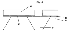
- FIG. 3 is a schematic cross sectional view of a semiconductor device of the present invention.
- FIGS. 4A to 4G are schematic cross sectional views for explaining a step of a manufacturing method for the semiconductor device of FIG. 3 ;
- FIG. 5 is a schematic view of a semiconductor device of the present invention.
- FIG. 6 is a graph showing the relationship between the threshold voltage of the transistor and the step.
- a step is formed in the border portion between the active region 5 and the insulating film 6 with which the trench region 4 is embedded during the step of forming a gate electrode 8 after the flattening step is completed.
- the step causes a step in the gate electrode 8 .
- the step in the gate electrode 8 causes partial concentration of an electrical field, and therefore, negatively affects the transistor properties. The adverse effects increase as an unit element becomes more miniaturized.
- the cause of the step varies.
- the step is formed when the insulating film 6 is removed using hydrogen fluoride or the like during the step of forming a gate insulating film 7 after the completion of the flattening step, and in other cases steps are formed when the insulating film 6 and the nitride film 3 in the border portions are excessively etched by hydrogen fluoride or the like, due to failure of the insulating film 6 in border portions between the nitride film 3 patterned above the active region 5 and the trench region 4 to be formed with the same film quality as in the flattened portions when the trench region 4 are embedded with the insulating film 6 .
- the step is formed when the insulating film is removed in the case where the time for removal is shorter.
- the time for removal is as short as currently possible in consideration of cost and environmental factors, and further reduction in the time for removal is difficult. Meanwhile, it is desired to keep the step caused by excessive etching to the minimum.
- FIG. 3 is a schematic cross sectional diagram showing the semiconductor device according to a desirable embodiment of the present invention
- the schematic cross sectional diagrams in FIGS. 4A to 4G schematically show the steps in the method for manufacturing the semiconductor device in FIG. 3 according to a desirable embodiment.
- the present invention is described in reference to FIGS. 3 and 4A to 4 G.
- a first insulating film 12 is formed on a semiconductor substrate 11 so as to make contact with the semiconductor substrate 11 ( FIG. 4A ).
- the semiconductor substrate is not particularly limited, as long as it can be used for a semiconductor device, and bulk substrates made of element semiconductors, such as silicon or germanium, or compound semiconductors, such as silicon germanium, can be cited as examples.
- the semiconductor material for forming the semiconductor substrate may be any of single crystal (formed through epitaxial growth, for example), polycrystal or amorphous crystal, though the amount of current flowing inside may be different.
- the first insulating film is selected from among insulating films having no difference in the polishing rate from that of the second insulating film, which is formed afterward. “No difference” means that the difference in the polishing rate between the two insulating films is within a range of ⁇ 50 nm/min under the same conditions for chemical mechanical polishing. As long as this condition is met, the first insulating film may be made of any insulating film having the same or different composition as the second insulating film.
- the combination of insulating films having different compositions expressed as “first insulating film/second insulating film”
- examples of the combinations include thermal oxide film/high density plasma CVD (HDP) film, plasma CVD (P-CVD) film/HDP film, and the like. It is preferable for the first insulating film to be an insulating film having the same composition as the second insulating film. Examples of insulating films having the same composition include silicon oxide films, HDP films, P-CVD films, and the like.
- the semiconductor substrate is a silicon substrate
- the first insulating film it is preferable for the first insulating film to be a silicon oxide film, and it is more preferable for it to be a silicon oxide film formed by thermally oxidizing a silicon substrate.
- the silicon oxide film it is preferable for the silicon oxide film to have a thickness of 2 nm to 30 nm when used as the first insulating film.
- the first insulating film 12 is processed to a mask for forming the trench region ( FIG. 4B ).
- the processing method is not particularly limited, and any publicly known method can be adopted.
- a method in which a resist pattern (not shown) may be formed on the first insulating film 12 in accordance with a photolithographic method, and this resist pattern used as a mask for etching can be cited as an example.
- Active regions 15 may include a wide active region (region where a large surface is secured for the semiconductor substrate) and a narrow active region (region where a small surface is secured for the semiconductor substrate).
- the semiconductor substrate 11 is selectively removed using the first insulating film 12 and the resist pattern as a mask, and thus, the trench region (field region) 14 can be formed in the semiconductor substrate 11 .
- the resist pattern is removed ( FIG. 4C ).
- the reference number 15 indicates an active region.
- the form of the trench region is not particularly limited, as long as it can electrically isolate a unit element to be formed afterward.
- the form of the trench region may be such that they are rectangles, trapezoids with a wider top than bottom, or upside-down triangles in a cross section, for example.
- the thickness of the trench region may be 5 nm to 50 nm, taking the electrically insulating properties between the unit elements into consideration, and it is preferable for the length of the bottom of the recesses to be 10 nm to 100 nm.
- the trench region may be formed in accordance with a method in which the resist pattern is removed and only the first insulating film 12 is used as a mask instead of a method in which both the first insulating film 12 and the resist pattern are used as a mask.
- the semiconductor substrate may be washed.
- an insulating film for example, a silicon oxide film formed through thermal oxidation
- a silicon oxide film formed through thermal oxidation may be formed in inner wall portions of the trench region 14 .
- a second insulating film 16 is formed on the semiconductor substrate 11 , including in the trench region 14 and on the first insulating film 12 , so as to make contact with these ( FIG. 4D ).
- the second insulating film is embedded in the trench region, and the top of the first insulating film is also almost covered.
- the unevenness of the base is reflected in the second insulating film formed on top, which has recesses above the trench region and a protrusion above the first insulating film.
- the second insulating film may be formed of an insulating film having the same composition or a different composition as the first insulating film.
- the semiconductor substrate is a silicon substrate
- the thickness of the silicon oxide film is not particularly limited when used as the second insulating film, as long as the trench region can be embedded with it. It is preferable for the thickness of the second insulating film formed the protrusion to be 50 nm to 300 nm between the upper surface of the first insulating film and the upper surface of the second insulating film with which the trench region is embedded.
- the second insulating film is an HDP-USG (high density plasma undoped silicate glass) film (non-doped silicon oxide film fabricated in accordance with high density plasma (HDP) CVD method).
- HDP-USG high density plasma undoped silicate glass
- HDP high density plasma
- the HDP CVD method is a method of performing deposition and etching of a film at the same time.
- This method is characterized in that the gap in a step portion having a high aspect ratio (trench region 14 ) can be effectively filled in. That is to say, in step portion adjacent to the trench region 14 , the rate of deposition of the second insulating film can be made very low.
- the second insulating film can be formed thin on top of the narrow active regions and thick on top of the wide active region.
- the portion of the second insulating film 16 that form the protrusion is removed so that the whole becomes level with the bottom of the recess (first removal step).
- the second insulating film 16 is removed until the level of the upper surface of the second insulating film 16 above the first insulating film 12 becomes the same as the upper surface of the second insulating film 16 in the trench region 14 .
- the end of removal need not be at the same point in time as when the level of the upper surface of the second insulating film 16 above the first insulating film 12 becomes the same as the level of the upper surface of the second insulating film in the trench region, and may be at the point in time when the second insulating film in the trench region is removed to a certain extent, as long as the level of the upper surface of the second insulating film in the trench region is higher than the upper surface of the first insulating film.
- the second insulating film in the trench region may be removed by approximately 20 nm to 30 nm.
- a publicly known method such as a CMP method can be exemplified.
- the end point for the first removal step can be detected in accordance with a technique for monitoring fluctuation in the pressure applied to the polishing pad when a CMP method used, for example.
- the polishing rate significantly lowers in the first removal step, and therefore, it becomes unnecessary to detect the end point when the time required for sufficiently removing the protrusion is preset.
- a slurry including abrasive particles can be used as the abrasive in accordance with the CMP method. It is preferable for the concentration of the abrasive particles in the slurry to be 0.5 to 1.5% by weight.
- the abrasive may include a surfactant and a solvent (for example, water) in addition to abrasive particles. It is preferable for the concentration of the surfactant to be 2 to 4% by weight.
- the abrasive particles, the surfactant and the water which form the abrasive may be separately dropped onto the semiconductor substrate or mixed before dropping.
- the abrasive particles are usually used together with a solvent in the form of a dispersing liquid. At this time, it is desirable for the pressure applied to the wafer to be 1 to 6 PSi.
- the first removal step is carried out under such conditions that the polishing rate for the second insulating film on top of the first insulating film to be greater than 0 nm/min and less than 50 nm/min.
- the polishing rate is within this range, the protrusion can be preferentially removed, so that flattening can be achieved.
- the first insulating film and the second insulating film are removed in accordance with a CMP method until they have a predetermined film thickness (second removal step).
- second removal step As a result of removal, the step formed by the recess and protrusion can be reduced to 20 nm or less. The reason why it is useful for the step to be 20 nm or less is described below.
- the removal of the first insulating film and the second insulating film is not particularly limited, and the second insulating film may be partially or entirely removed, or the second insulating film may be entirely removed while the first insulating film is partially or entirely removed. It is preferable for the amount of removal of the first insulating film to be determined by the necessary amount of removal of the insulating film for preventing the active regions from being exposed before the formation of the gate insulating film when a transistor is subsequently formed, for example.
- the first insulating film can be removed so that approximately 10 to 30 nm remain, for example.
- no stopper film is used, and thus, the state where there are no step in the end portion of the trench region at the stage where the second removal step is completed can be maintained until the subsequent element forming step (for example, gate electrode film forming step).
- the polishing rate in the second removal step is faster than in the first removal step. Concretely, it is preferable to set the polishing rate to approximately 50 nm/min to 500 nm/min, and it is more preferable to set approximately at 200 nm/min to 300 nm/min. When the polishing rate is within this range, the amount of scratching after the first removal step can be set at 1/100 or less while controlling the thickness of the insulating film above the semiconductor substrate.
- the upper surface formed of the second insulating film or the first insulating film and the setting insulating film is approximately flat after the first removal step, and there is substantially no step in the end portion of the trench region.
- the first insulating film and the second insulating film are formed of insulating films having no difference in the polishing rate, and therefore, the step in the end portion of the trench region can be made significantly small in comparison with conventional cases, where there is a difference between the insulating films. Accordingly, the polishing rate for the insulating films can be made the same on top of the first insulating film and on top of the trench region in the second removal step, as compared to in the prior art, where a stopper film is used.
- a slurry including abrasive particles (for example, cerium oxide particles) is used as the abrasive in the CMP method. It is preferable for the concentration of the abrasive particles in the slurry to be 0.2 to 0.6% by weight.
- the abrasive may include a surfactant and a solvent (for example, water) in addition to abrasive particles. It is preferable for the concentration of the surfactant to be 0.2 to 1.2% by weight.
- the abrasive particles, the surfactant and the water which form the abrasive may be separately dropped onto the semiconductor substrates or mixed before dropping. In the case where they are separately dropped, the abrasive particles are usually used together with a solvent in the form of a dispersing liquid. At this time, it is desirable for the pressure applied to the wafer to be 1 PSi to 6 PSi.
- the first removal step and the second removal step can be carried out continuously.
- the device for the CMP method prefferably be such a device that the amount of abrasive particle dispersing liquid, surfactant and water dropped can be changed, in order to carry out the first and second removal steps continuously.
- the depth and width of scratches formed in the first removal step can be made greater through etching in a washing step (for example, washing using hydrogen fluoride (HF)) which may or may not be carried out after polishing.
- a washing step for example, washing using hydrogen fluoride (HF)
- HF hydrogen fluoride
- polishing in the second removal step is carried out discontinuously in this state, there is a possibility that abrasive particles may remain in the grooves of the expanded scratches. Such residue can be prevented by carrying out the first and second removal steps continuously.
- the unit element can be formed in the active region 15 by carrying out the steps in accordance with the unit element which is desired to be formed.
- the unit element is transistor
- the first insulating film 12 remaining in the active region 15 after the second removal step is entirely removed using HF or DHF (diluted HF). Thereafter, thermal oxidation is performed again so as to form an oxide film in the active region.
- a photoresist mask having a pattern for forming a well region is formed in a predetermined region, and ions are implanted via the photoresist mask, so that the well region is formed. Appropriate conditions can be set for ion implantation in accordance with the performance of the desired transistor.
- the oxidation film in the active region 15 is entirely removed using HF or DHF ( FIG. 4F ).
- a gate insulating film 17 and gate electrode 18 are formed on the active region 15 after the removal of the oxide film ( FIGS. 3 and 4G ). Thereafter, source/drain regions 19 are formed in accordance with a predetermined method, and thus, the transistor can be obtained.
- FIGS. 5 a and 5 b show an example of the obtained transistor.
- FIG. 5 a is a schematic plan diagram showing a transistor
- FIG. 5 b is a schematic cross sectional diagram along A-B showing the transistor in FIG. 5 a
- FIG. 5 c is a schematic cross sectional diagram along C-D showing the transistor in FIG. 5 a.
- FIG. 5 d is a schematic cross sectional diagram along A-B after the additional formation of a wire layer in the transistor in FIG. 5 a
- FIG. 5 e is a schematic cross sectional diagram along C-D after the additional formation of a wire layer in the transistor in FIG. 5 a .
- a well-known method can be adopted as the method for forming the interlayer insulating film, the contact and the wiring layer.
- transistor is cited as examples of the unit element in the above, other unit elements, such as capacitor, diode, thyristor, resistor and wire can be formed in the active region obtained in accordance with the manufacturing method of the present invention.
- FIG. 6 is a graph showing the relationship between the threshold voltage of the transistor and the step.
- the seven types of transistors for which the threshold voltage is plotted in FIG. 6 have the same configuration, except that the size of the steps is different.
- a silicon substrate is used as the semiconductor substrate
- a silicon oxide film formed in accordance with a thermal oxidation method so as to have a thickness of 2 nm is used as the gate insulating film
- a polysilicon film having a thickness of 20 nm is used as the gate electrode
- impurity regions of 1 E 15 cm ⁇ 3 impurity species: B+, P+, As+
- a silicon oxide film formed in accordance with an HDPCVD method is used as the second insulating film
- the gate length is approximately 0.1 ⁇ m
- the gate width is 1.0 ⁇ m.
- the steps can be adjusted through wet etching using hydrogen fluoride or in accordance with a CMP method.
- adjustment through wet etching makes for the least inconsistency, and thus is most appropriate.
- the case where the step is 0 nm means in a state in which there are no steps between the active region and the trench region, so that the two regions are in a horizontal state.
- the case where the step is smaller than 0 nm means a state in which the active region is lower than the trench region, and an insulating film (first insulating film or first insulating film and second insulating film) remains in the active region.
- the electrical field is concentrated in the border portion between the active region and the trench region on the silicon substrate.
- the threshold value is outside the allowable range of ⁇ 10% as specified for the dispersion.
- the state becomes such that the insulating film formed in a preceding step, before the formation of the gate insulating film, remains on the silicon substrate, and the transistor malfunctions.
- the unit element is the transistor
- the flatness after use of the CMP method can be maintained until the time when the gate electrode is formed.
- the step is reduced in the interface between the active region and the element isolation region, so that concentration of an electrical field resulting from the step in the gate electrode can be lessened, and thus, the transistor properties can be improved.
Abstract
Description
Claims (7)
Applications Claiming Priority (2)
| Application Number | Priority Date | Filing Date | Title |
|---|---|---|---|
| JP2007-295890 | 2007-11-14 | ||
| JP2007295890A JP2009123890A (en) | 2007-11-14 | 2007-11-14 | Semiconductor device and manufacturing method thereof |
Publications (2)
| Publication Number | Publication Date |
|---|---|
| US20090121310A1 US20090121310A1 (en) | 2009-05-14 |
| US7736990B2 true US7736990B2 (en) | 2010-06-15 |
Family
ID=40622925
Family Applications (1)
| Application Number | Title | Priority Date | Filing Date |
|---|---|---|---|
| US12/270,659 Active US7736990B2 (en) | 2007-11-14 | 2008-11-13 | Semiconductor device and manufacturing method for the same |
Country Status (2)
| Country | Link |
|---|---|
| US (1) | US7736990B2 (en) |
| JP (1) | JP2009123890A (en) |
Families Citing this family (3)
| Publication number | Priority date | Publication date | Assignee | Title |
|---|---|---|---|---|
| US9391159B2 (en) | 2012-04-03 | 2016-07-12 | Taiwan Semiconductor Manufacturing Company, Ltd. | Triple well isolated diode and method of making |
| DE102020112203A1 (en) | 2020-03-13 | 2021-09-16 | Taiwan Semiconductor Manufacturing Co. Ltd. | METHOD OF EMBEDDING PLANAR FETS WITH FINFETS |
| US11355493B2 (en) | 2020-03-13 | 2022-06-07 | Taiwan Semiconductor Manufacturing Company, Ltd. | Method to embed planar FETs with finFETs |
Citations (5)
| Publication number | Priority date | Publication date | Assignee | Title |
|---|---|---|---|---|
| JPH10189708A (en) | 1996-12-17 | 1998-07-21 | Samsung Electron Co Ltd | Trench element isolating method |
| JP2002252279A (en) | 2001-01-12 | 2002-09-06 | Tobu Denshi Kk | Element isolation film forming method for semiconductor device |
| US20040232513A1 (en) * | 2003-05-23 | 2004-11-25 | Taiwan Semiconductor Manufacturing Co. | Silicon strain engineering accomplished via use of specific shallow trench isolation fill materials |
| JP2005175110A (en) | 2003-12-10 | 2005-06-30 | Matsushita Electric Ind Co Ltd | Method for manufacturing semiconductor device |
| US20060134850A1 (en) * | 2004-12-22 | 2006-06-22 | Dongbuanam Semiconductor Inc. | Method of manufacturing a high voltage semiconductor device including a deep well and a gate oxide layer simultaneously |
-
2007
- 2007-11-14 JP JP2007295890A patent/JP2009123890A/en active Pending
-
2008
- 2008-11-13 US US12/270,659 patent/US7736990B2/en active Active
Patent Citations (5)
| Publication number | Priority date | Publication date | Assignee | Title |
|---|---|---|---|---|
| JPH10189708A (en) | 1996-12-17 | 1998-07-21 | Samsung Electron Co Ltd | Trench element isolating method |
| JP2002252279A (en) | 2001-01-12 | 2002-09-06 | Tobu Denshi Kk | Element isolation film forming method for semiconductor device |
| US20040232513A1 (en) * | 2003-05-23 | 2004-11-25 | Taiwan Semiconductor Manufacturing Co. | Silicon strain engineering accomplished via use of specific shallow trench isolation fill materials |
| JP2005175110A (en) | 2003-12-10 | 2005-06-30 | Matsushita Electric Ind Co Ltd | Method for manufacturing semiconductor device |
| US20060134850A1 (en) * | 2004-12-22 | 2006-06-22 | Dongbuanam Semiconductor Inc. | Method of manufacturing a high voltage semiconductor device including a deep well and a gate oxide layer simultaneously |
Also Published As
| Publication number | Publication date |
|---|---|
| JP2009123890A (en) | 2009-06-04 |
| US20090121310A1 (en) | 2009-05-14 |
Similar Documents
| Publication | Publication Date | Title |
|---|---|---|
| KR102474431B1 (en) | Method of manufacturing semiconductor devices | |
| US6326283B1 (en) | Trench-diffusion corner rounding in a shallow-trench (STI) process | |
| KR100473733B1 (en) | Semiconductor device and method for manufacturing the same | |
| US9601568B2 (en) | Semiconductor device including STI structure | |
| KR100341480B1 (en) | Method for self-aligned shallow trench isolation | |
| KR100335495B1 (en) | Simplified method of manufacturing isolation layer preventing divot generation | |
| US6656793B2 (en) | Method of forming a self-aligned floating gate in flash memory cell | |
| US6107140A (en) | Method of patterning gate electrode conductor with ultra-thin gate oxide | |
| US7736990B2 (en) | Semiconductor device and manufacturing method for the same | |
| JP2006013422A (en) | Semiconductor device and its manufacturing method | |
| KR20010046153A (en) | Method of manufacturing trench type isolation layer in semiconductor device | |
| US6586313B2 (en) | Method of avoiding the effects of lack of uniformity in trench isolated integrated circuits | |
| KR20010055525A (en) | Method for shallow trench isolation | |
| KR100671603B1 (en) | Method of manufacturing a flash memory device | |
| US7214596B2 (en) | Method for the fabrication of isolation structures | |
| KR100427537B1 (en) | Method of forming a isolation layer in a semiconductor device and manufacturing a flash memory cell using the same | |
| JP3397693B2 (en) | Semiconductor device and manufacturing method thereof | |
| KR100824153B1 (en) | Method of manufacturing a semiconductor device | |
| KR100400301B1 (en) | A method for forming a field oxide of semiconductor device | |
| KR20040005230A (en) | Method for manufacturing flash memory | |
| KR101004810B1 (en) | Method for forming isolation of semiconductor device | |
| KR100588646B1 (en) | Method for fabricating isolation of semiconductor device | |
| KR100444016B1 (en) | Semiconductor fabrication method for improving operational characteristics of transistor | |
| KR100821488B1 (en) | Method for manufacturing isolation of a semiconductor device | |
| KR100932336B1 (en) | Device Separating Method of Flash Memory Device |
Legal Events
| Date | Code | Title | Description |
|---|---|---|---|
| AS | Assignment |
Owner name: SHARP KABUSHIKI KAISHA, JAPAN Free format text: ASSIGNMENT OF ASSIGNORS INTEREST;ASSIGNOR:YAMAUCHI, HIROSHI;REEL/FRAME:021983/0813 Effective date: 20081113 Owner name: SHARP KABUSHIKI KAISHA,JAPAN Free format text: ASSIGNMENT OF ASSIGNORS INTEREST;ASSIGNOR:YAMAUCHI, HIROSHI;REEL/FRAME:021983/0813 Effective date: 20081113 |
|
| STCF | Information on status: patent grant |
Free format text: PATENTED CASE |
|
| FEPP | Fee payment procedure |
Free format text: PAYER NUMBER DE-ASSIGNED (ORIGINAL EVENT CODE: RMPN); ENTITY STATUS OF PATENT OWNER: LARGE ENTITY Free format text: PAYOR NUMBER ASSIGNED (ORIGINAL EVENT CODE: ASPN); ENTITY STATUS OF PATENT OWNER: LARGE ENTITY |
|
| FPAY | Fee payment |
Year of fee payment: 4 |
|
| MAFP | Maintenance fee payment |
Free format text: PAYMENT OF MAINTENANCE FEE, 8TH YEAR, LARGE ENTITY (ORIGINAL EVENT CODE: M1552) Year of fee payment: 8 |
|
| MAFP | Maintenance fee payment |
Free format text: PAYMENT OF MAINTENANCE FEE, 12TH YEAR, LARGE ENTITY (ORIGINAL EVENT CODE: M1553); ENTITY STATUS OF PATENT OWNER: LARGE ENTITY Year of fee payment: 12 |