US7728689B2 - Pulse width modulator system - Google Patents
Pulse width modulator system Download PDFInfo
- Publication number
- US7728689B2 US7728689B2 US11/596,606 US59660607A US7728689B2 US 7728689 B2 US7728689 B2 US 7728689B2 US 59660607 A US59660607 A US 59660607A US 7728689 B2 US7728689 B2 US 7728689B2
- Authority
- US
- United States
- Prior art keywords
- pulse width
- signal
- width modulator
- amplitude
- input signal
- Prior art date
- Legal status (The legal status is an assumption and is not a legal conclusion. Google has not performed a legal analysis and makes no representation as to the accuracy of the status listed.)
- Expired - Fee Related, expires
Links
Images


Classifications
-
- H—ELECTRICITY
- H03—ELECTRONIC CIRCUITRY
- H03F—AMPLIFIERS
- H03F1/00—Details of amplifiers with only discharge tubes, only semiconductor devices or only unspecified devices as amplifying elements
- H03F1/32—Modifications of amplifiers to reduce non-linear distortion
-
- H—ELECTRICITY
- H03—ELECTRONIC CIRCUITRY
- H03F—AMPLIFIERS
- H03F3/00—Amplifiers with only discharge tubes or only semiconductor devices as amplifying elements
- H03F3/20—Power amplifiers, e.g. Class B amplifiers, Class C amplifiers
- H03F3/21—Power amplifiers, e.g. Class B amplifiers, Class C amplifiers with semiconductor devices only
- H03F3/217—Class D power amplifiers; Switching amplifiers
-
- H—ELECTRICITY
- H04—ELECTRIC COMMUNICATION TECHNIQUE
- H04L—TRANSMISSION OF DIGITAL INFORMATION, e.g. TELEGRAPHIC COMMUNICATION
- H04L25/00—Baseband systems
- H04L25/38—Synchronous or start-stop systems, e.g. for Baudot code
- H04L25/40—Transmitting circuits; Receiving circuits
- H04L25/49—Transmitting circuits; Receiving circuits using code conversion at the transmitter; using predistortion; using insertion of idle bits for obtaining a desired frequency spectrum; using three or more amplitude levels ; Baseband coding techniques specific to data transmission systems
- H04L25/4902—Pulse width modulation; Pulse position modulation
-
- H—ELECTRICITY
- H03—ELECTRONIC CIRCUITRY
- H03F—AMPLIFIERS
- H03F2200/00—Indexing scheme relating to amplifiers
- H03F2200/114—Indexing scheme relating to amplifiers the amplifier comprising means for electro-magnetic interference [EMI] protection
-
- H—ELECTRICITY
- H03—ELECTRONIC CIRCUITRY
- H03F—AMPLIFIERS
- H03F2200/00—Indexing scheme relating to amplifiers
- H03F2200/351—Pulse width modulation being used in an amplifying circuit
Definitions
- the present invention relates to a pulse width modulator system comprising an amplitude distribution filter.
- U.S. Pat. No. 5,617,058 discloses a method of minimizing nonlinearities when amplifying pulse width modulated (PWM) signals.
- a problem of the disclosed invention is that it requires complex and power consuming compensation to be performed in the pulse width modulator.
- a further problem is that the compensation performed causes a worsening of the electromagnetic compatibility and interference (EMC/EMI) properties.
- EMC/EMI electromagnetic compatibility and interference
- the invention relates to a pulse width modulator system PWMS comprising
- an advantageous means for modifying a signal to better allow for processing or other kinds of handling by means that do not process all possible signal amplitudes linearly is provided.
- the concentration of signal amplitudes that may be problematic to handle properly by a subsequent means is reduced.
- the present invention is especially beneficial when used with connection to PWM amplifiers of other uses of pulse width modulation, as too narrow PWM pulses may often be handled improperly.
- By means of the present invention it is possible to prevent too narrow pulses to be established, or at least reduce the concentration of such pulses.
- the present invention may however as well be used for preventing or reducing the concentration of pulses of any predetermined pulse widths. Also in systems where the end product is not pulses, the present invention may be used for preventing or reducing the concentration of occurrences within predetermined ranges.
- the term predetermined is to be understood in a broad sense, thus not necessarily corresponding to the term fixed.
- the manufacturer or user may actually fix the predetermined amplitude range, or it may be determined from time to time during use, e.g. by adapting to changing environmental or internal parameters, or due to external control.
- pulse width modulation is to be understood in a broad sense referring to any possible category of pulse width modulation, comprising, e.g., by sampling method: naturally sampled PWM and uniformly sampled PWM, by signal parts: single sided PWM and double sided PWM, and by encoding: two-level PWM, three-level PWM, etc.
- the pulse width modulator PMOD may be any kind of means suitable for establishing a pulse width modulated representation of a signal. Which kind of pulse width modulator to use in a particular application depends on the type of input signal, the desired precision and signal/error-ratio, as well as the desired type of PWM to be established.
- the pulse width modulator may be of a type operating on the basis of a reference signal, a reference signal representation, i.e. a model of a reference signal, or no reference signal at all.
- the pulse width modulator may be implemented as an all-analog circuit, all-digital circuit, software executable, or any kind of hybrid implementation.
- the different system parts may be physically implemented within a single package, e.g. an integrated circuit, but they may as well be implemented as individual building blocks, whether as integrated circuits or by means of discrete components.
- the amplitude distribution filter ADF may be positioned anywhere in the input signal path, and not necessarily in connection with the pulse width modulator and probably a PWM amplifier. This feature is made possible by the present invention offering pre-processing of a signal that at some point are to be processed by means comprising non-linear processing within certain amplitude ranges.
- setups comprising further processing blocks between the amplitude distribution filter ADF and the pulse width modulator PMOD is within the scope of the present invention.
- said pulse width modulator system PWMS comprises an amplifier AMP, comprising an amplifier output AMPO, said amplifier producing an amplified modulator system output signal MSOS on said amplifier output AMPO responsive to said modulator output signal MOS, an advantageous embodiment of the present invention has been obtained.
- amplifying the modulator output signal MOS is typically referred to increasing the amplitude of the PWM pulses.
- any kind of amplifier may be used for amplifying the PWM signal.
- said amplifier AMP is a switching amplifier
- switching amplifiers are the most cost-effective means for amplifying a PWM signal.
- any kind of switching amplifier may be used, e.g. simple electrically or electronically switches, power electronic switches, e.g. power transistors, complex switch setups such as h-bridges, etc.
- the input signal may be a continuous time signal, e.g. from the output of an analog audio media reading means or any other kind of analog and/or continuous time signal.
- the input signal is preferably a discrete time signal, such as e.g. a sampled signal or the output of a true digital audio processing means.
- the input signal may e.g. be a pulse code modulated (PCM) signal.
- PCM pulse code modulated
- the utility content of the input signal is preferably audio of any kind, i.e. representing a utility band of 20 kHz, preferably 48 kHz, and even more preferably 96 kHz.
- the modulator output signal MOS established by the pulse width modulator PMOD is preferably a PWM signal.
- said pulse width modulated signal comprises at least partly curved or inclined pulses
- an advantageous embodiment of the present invention has been obtained.
- non-square shapes may be used for establishing the PWM pulses.
- the PWM signal is preferably a three level PWM signal, and preferably encoded on two signal carriers whereof a first carries pulses representing positive input signal amplitudes and a second carries pulses representing negative input signal amplitudes whereby the two signal carriers preferably never simultaneously comprise pulses.
- Any kind of three level PWM signals may however be used with the present invention, as well as two level or multiple level signals.
- the predetermined amplitude range may be moved among the possible signal amplitudes during use.
- the extent, i.e. the values of the low and high thresholds LT, HT, relative to each other, of the predetermined amplitude range may be changed during use.
- said at least one predetermined amplitude range comprises the zero-level
- an advantageous embodiment of the present invention has been obtained.
- the predetermined amplitude range preferably comprises the zero-level, as it is around that level most PWM amplifiers process data non-linearly.
- the predetermined amplitude range is preferably symmetric around the zero-level, as this is one of the typical properties of most PWM amplifiers' non-linear processing range.
- said at least one predetermined amplitude range comprises a range from a low threshold LT up to but not including the zero-level, and a range from but not including the zero-level up to a high threshold HT, an advantageous embodiment of the present invention has been obtained.
- the exact zero-level is often not included in the non-linear processing range of a processing means, even if both sides of it are. Hence a preferred embodiment of the present invention that utilizes this fact is provided.
- a preferred embodiment is obtained by determining the predetermined amplitude range on the minimum width of the PWM pulses in the modulator output signal MOS.
- an even more preferred embodiment is obtained by determined the minimum pulse widths on the basis of characteristics of the amplifier.
- said characteristics of said amplifier AMP comprises the rise time and/or fall time, an advantageous embodiment of the present invention has been obtained.
- an embodiment of the present invention allows, e.g., an external control unit to dynamically adapt the predetermined amplitude ranges.
- a multiple channel PWM amplifier comprising several pulse width modulator systems according to the present invention, uses a shared control unit to dynamically adapt the predetermined amplitude ranges of each modulator system in order to avoid concurrent flanks in the different channels. Thereby, e.g., cross talk is reduced.
- said amplitude distribution filter ADF comprises a signal generator SG adapted for establishing an outband signal OBS, an advantageous embodiment of the present invention has been obtained.
- said amplitude distribution filter ADF comprises a level controlled generator LCG adapted for establishing an outband signal OBS at least partly controlled on the basis of the amplitude of said input signal IS, an advantageous embodiment of the present invention has been obtained.
- characteristics of the outband signal are controlled on the basis of the amplitude of the input signal.
- the outband signal amplitude varying with the input signal amplitude is to be understood in a loose sense, as this does not necessarily mean that the amplitudes follows each other by a fixed offset.
- the correspondence between the outband signal amplitude and the input signal amplitude is preferably changed according to the input signal amplitude.
- the outband signal amplitude in an embodiment varies tightly with the input signal amplitude, as it is determined only by adding an offset to the input signal amplitude.
- said outband signal OBS comprises a frequency corresponding to the half of the modulation frequency of said pulse width modulator PMOD, an advantageous embodiment of the present invention has been obtained.
- outband signal frequency of half the PWM frequency it may for several simple outband signal wave form types be ensured that the outband signal amplitude peaks alternates between a high and a low peak with one such peak for each PWM period.
- the performance of the amplitude distribution filter is improved.
- said outband signal OBS comprises a frequency corresponding to the quarter of the modulation frequency of said pulse width modulator PMOD, an advantageous embodiment of the present invention has been obtained.
- the intermediate output signal amplitude for each four PWM periods has the values: high peak, zero, low peak, zero.
- the performance of the amplitude distribution filter is improved, as well as a reduction of the power dissipation in the amplifier due to the absence of pulses on zero-level input.
- the wave form of said outband signal OBS is a sine waveform, a triangular waveform, a square waveform or a sawtooth waveform, an advantageous embodiment of the present invention has been obtained.
- simple periodic signals are preferred in order to prioritize simple and cost-effective implementation.
- an outband signal comprising multiple frequencies is preferred in order to prioritize electromagnetic compatibility and interference (EMC/EMI) properties, as well as reducing the errors introduced when the outband signal is correlated to the input signal.
- EMC/EMI electromagnetic compatibility and interference
- the broader frequency band comprised by the outband signal the better EMC/EMI properties.
- the frequency spectrum of the outband signal should preferably be shaped by reducing the utility band concentration.
- the outband signal should preferably be synchronized with the PWM frequency.
- Such synchronization may comprise direct synchronization between the outband signal and the PWM frequency or it may comprise indirect synchronization where the outband signal is established in such a way that the intermediate output signal becomes synchronized with the PWM frequency.
- said synchronization comprises synchronizing the peaks of said outband signal OBS with the modulation frequency and modulation phase of said pulse width modulator PMOD, an advantageous embodiment of the present invention has been obtained.
- the outband signal amplitude peaks, or preferably the intermediate output signal amplitude peaks alternates between a high and a low peak with one such peak for each PWM period, or that the outband signal amplitude, or preferably the intermediate output signal amplitude, for each four PWM periods has the values: high peak, zero, low peak, zero, the performance of the amplitude distribution filter is improved.
- synchronization with the modulation phase is referred to synchronizing the outband peaks with the times in each PWM period where the input signal is considered or sampled, or more preferably establishing an outband signal that causes the intermediate output signal peaks to be synchronized with the times in each PWM period where the signal is considered or sampled by the pulse width modulator PMOD.
- said pulse width modulator PMOD comprises a reference signal representation generator 15 establishing a reference signal representation
- the pulse width modulator may determine the times of the PWM pulse flanks by comparing the utility signal with a reference signal representation.
- This reference signal representation may be a physical signal or a model of a such comprising polynomials or a table of values.
- said synchronization comprises synchronizing the outband signal OBS with said reference signal representation of said pulse width modulator PMOD, an advantageous embodiment of the present invention has been obtained.
- Such synchronization may comprise direct synchronization between the outband signal and the reference signal or it may comprise indirect synchronization where the outband signal is established in such a way that the intermediate output signal becomes synchronized with the reference signal.
- said amplitude distribution filter ADF further comprises a noise shaper performing noise shaping of said intermediate output signal OS, preferably errors introduced by the addition of said outband signal OBS, an advantageous embodiment of the present invention has been obtained.
- said noise shaper comprises a loop filter LF, a filter summing point 63 , 82 , 103 , 143 , 162 , 183 , 223 and a feedback summing point 61 , 81 , 101 , 141 , 161 , 181 , 221 establishing a feedback path from said intermediate output signal OS to said input signal IS, an advantageous embodiment of the present invention has been obtained.
- noise shaper embodiment is preferred. It is however noted that any kind of noise shaper implementation is within the scope of the present invention.
- said loop filter LF comprises a low pass filter, preferably a low-pass infinite impulse response filter with a corner frequency at preferably 20 kHz, an advantageous embodiment of the present invention has been obtained.
- the above described loop filter embodiment is preferred. It is however noted that any kind of loop filter implementation is within the scope of the present invention. Also a distribution of parts the loop filter or a relocation of the whole loop filter to different positions in the circuit is within the scope of the present invention.
- mapping means MM adapted for establishing a mapping output 83 , 163 corresponding to said input signal IS in such a way that input signal amplitude instances that fall within said at least one predetermined amplitude range are mapped to mapping output amplitude instances according to a predetermined mapping scheme
- mapping means may be any suitable means for performing the described mapping, whether analog, digital or software based.
- Such means may, e.g., comprise table lookups, “if-else” conditional structures, “switch-case” conditional structures or any other suitable means.
- said predetermined mapping scheme comprises mapping input signal amplitude instances that fall within said at least one predetermined amplitude range to amplitude instances outside said at least one predetermined amplitude range, an advantageous embodiment of the present invention has been obtained.
- input signal amplitudes within the predetermined amplitude range are in the mapping output 83 , 163 mapped to amplitudes outside the predetermined amplitude range.
- said predetermined mapping scheme comprises mapping input signal amplitude instances that fall within said at least one predetermined amplitude range to the zero-level, an advantageous embodiment of the present invention has been obtained.
- input signal amplitudes within the predetermined amplitude range are in the mapping output 83 , 163 mapped to the zero-level, which may cause several PWM-periods to comprise no pulse. This may in certain applications cause a considerable saving on amplifier power consumption.
- the predetermined mapping scheme may be dynamically adapted, preferably in order to adapt to changes in the predetermined amplitude range.
- an embodiment of the present invention allows, e.g., an external control unit to dynamically adapt the predetermined mapping scheme.
- said amplitude distribution filter ADF further comprises a quantizer QZ, an advantageous embodiment of the present invention has been obtained.
- a quantizer is implemented in a preferred embodiment.
- the noise shaping capabilities of preferred embodiments are also applied to the quantization errors inherently introduced by any quantization.
- said modifying the level of the amplitude distribution of said input signal IS within said at least one predetermined amplitude range comprises decreasing said level of the amplitude distribution of said input signal IS within said at least one predetermined amplitude range, an advantageous embodiment of the present invention has been obtained.
- pulse width modulator PMOD comprises an intersection computing block 12 .
- the intersection computing block may be any suitable means for measuring, monitoring, estimating, computing, etc., the times of intersection between two signals.
- Such means may, e.g., comprise comparators, logical gates or software-based routines, or any other suitable implementation.
- said pulse width modulator PMOD comprises a pulse generator 14
- the pulse generator may be any means suitable for establishing PWM pulses.
- the present invention further relates to a pulse width modulator system PWMS comprising
- FIG. 1A illustrates an embodiment of the present invention
- FIG. 1B illustrates an embodiment of the present invention shown in a context
- FIG. 1C illustrates an embodiment of a pulse width modulator PMOD
- FIG. 2A to 2D illustrate a possible effect of non-linear processing
- FIG. 3A illustrates an ideal output/input relationship
- FIG. 3B illustrates an output/input relationship comprising a non-linear range
- FIG. 4A to 4F illustrate a reference output signal amplitude distribution
- FIG. 5A illustrates an embodiment of an amplitude distribution filter ADF according to the present invention
- FIG. 5B to 5G illustrate possible effects of the embodiment of FIG. 5A .
- FIG. 6A illustrates a further embodiment of an amplitude distribution filter ADF according to the present invention
- FIG. 6B graphically illustrates a possible outband signal level control algorithm
- FIG. 6C to 6E illustrate possible effects of the embodiment of FIG. 6A .
- FIG. 7A illustrates a possible input signal IS to the embodiment of FIG. 6A .
- FIG. 7B illustrates a possible outband signal OBS established by the embodiment of FIG. 6A .
- FIG. 7C illustrates a possible output signal OS provided by the embodiment of FIG. 6A .
- FIG. 7D to 7I illustrate the output signal amplitude distribution according to the embodiment of FIG. 6A .
- FIG. 8A illustrates a further embodiment of an amplitude distribution filter ADF according to the present invention
- FIG. 8B to 8C illustrate a possible mapping scheme
- FIG. 9A illustrates a possible input signal IS to the embodiment of FIG. 8A .
- FIG. 9B illustrates a possible output signal OS provided by the embodiment of FIG. 8A .
- FIG. 9C to 9H illustrate the output signal amplitude distribution according to the embodiment of FIG. 8A .
- FIG. 10 illustrates a preferred embodiment of the amplitude distribution filter ADF of the present invention
- FIG. 11A illustrates a possible input signal IS to the embodiment of FIG. 10 .
- FIG. 11B illustrates a possible outband signal OBS established by the embodiment of FIG. 10 .
- FIG. 11C illustrates a possible output signal OS provided by the embodiment of FIG. 10 .
- FIG. 11D to 11I illustrate the output signal amplitude distribution according to the embodiment of FIG. 10 .
- FIG. 12 to 13 illustrate possible relative output signal noise floors
- FIG. 14A illustrates a further embodiment of an amplitude distribution filter ADF according to the present invention
- FIG. 14B to 14D illustrate possible effects of the embodiment of FIG. 14A .
- FIG. 15A illustrates a possible input signal IS to the embodiment of FIG. 14A .
- FIG. 15B illustrates a possible outband signal OBS established by the embodiment of FIG. 14A .
- FIG. 15C illustrates a possible output signal OS provided by the embodiment of FIG. 14A .
- FIG. 15D to 15J illustrate the output signal amplitude distribution according to the embodiment of FIG. 14A .
- FIG. 16A illustrates a further embodiment of an amplitude distribution filter ADF according to the present invention
- FIG. 16B to 16C illustrate a possible mapping scheme
- FIG. 17A illustrates a possible input signal IS to the embodiment of FIG. 16A .
- FIG. 17B illustrates a possible output signal OS provided by the embodiment of FIG. 16A .
- FIG. 17C to 17H illustrate the output signal amplitude distribution according to the embodiment of FIG. 16A .
- FIG. 18 illustrates a preferred embodiment of the amplitude distribution filter ADF of the present invention
- FIG. 19A illustrates a possible input signal IS to the embodiment of FIG. 18 .
- FIG. 19B illustrates a possible outband signal OBS established by the embodiment of FIG. 18 .
- FIG. 19C illustrates a possible output signal OS provided by the embodiment of FIG. 18 .
- FIG. 19D to 19I illustrate the output signal amplitude distribution according to the embodiment of FIG. 18 .
- FIG. 20 to 21 illustrate possible relative output signal noise floors
- FIG. 22A illustrates a further preferred embodiment of the amplitude distribution filter ADF of the present invention
- FIG. 22B graphically illustrates a possible outband signal level control algorithm
- FIG. 22C illustrates a possible effect of the embodiment of FIG. 22A .
- FIG. 23A illustrates an output/input relationship comprising several non-linear ranges
- FIG. 23B illustrates an output/input relationship comprising a dynamically positioned non-linear range
- FIG. 24 illustrates an embodiment of a multi-channel pulse width modulator system MCS.
- FIG. 1A illustrates an embodiment of a pulse width modulator system PWMS of the present invention. It comprises a modulator input MI receiving an input signal IS.
- the input signal may is preferably the utility signal to be pulse width modulated.
- An amplitude distribution filter ADF of the present invention processes the input signal IS in order to adapt the input signal amplitude distribution to achieve the best performance of subsequent stages.
- the amplitude distribution filter ADF establishes an output signal OS, also referred to as intermediate output signal, which is fed to a pulse width modulator PMOD.
- the pulse width modulator PMOD establishes a pulse width modulated representation of the output signal, and outputs it via a modulator output MO as a modulator output signal MOS.
- FIG. 1B illustrates a further embodiment of a pulse width modulator system PWMS of the present invention, and a context for its use. It comprises all elements of FIG. 1A coupled as described above. It furthermore comprise an amplifier AMP received the modulator output MOS.
- the amplifier is preferably of the power switch type, but may be any amplifier suited for amplifying a PWM signal.
- the amplifier may comprise any number of switches and couplings of these, in accordance with the type of PWM modulation scheme used by the PWM modulator PMOD.
- the amplifier outputs a modulator system output signal MSOS via an amplifier output AMPO.
- the modulator system output signal MSOS being the output of the pulse width modulator system PWMS of the present embodiment is preferably demodulated by means of a demodulator DEM, typically a low-loss, low-pass filter, and is fed to a loudspeaker LS.
- a demodulator DEM typically a low-loss, low-pass filter
- LS loudspeaker
- the amplifier, demodulator and loudspeaker may be coupled in any way suitable. This particularly applies for systems where the PWM signal is distributed over two or more simultaneous signal parts, e.g. as typically used for three level PWM signals.
- FIG. 1C illustrates a further embodiment of a pulse width modulator system PWMS of the present invention, and in particular is illustrates an example of an embodiment of the pulse width modulator PMOD.
- the illustrated system comprises a PWM amplifier/audio system for use with a discrete time input signal, e.g. a pulse code modulated (PCM) signal.
- PCM pulse code modulated
- the present embodiment comprises a modulator system input MI feeding an input signal IS to an amplitude distribution filter ADF.
- the intermediate output signal OS of the amplitude distribution filter ADF is fed to the pulse width modulator PMOD.
- the modulator output MOS of the pulse width modulator PMOD i.e. a pulse width modulated signal
- FIG. 1C further illustrates an embodiment of a pulse width modulator PMOD. It comprises an upsampling block 11 basically transforming the intermediate output signal OS from one sampling frequency representation into an N times higher sampling representation.
- the upsampled signal is then fed to an intersection-computing block 12 adapted for determination of intersections with a parallel reference signal representation 16 provided by a reference signal generator 15 .
- the intersections may e.g. be established in the block 12 according to the principles disclosed in PCT/DK03/00334 hereby incorporated by reference, or in PCT/DK2004/000361 hereby incorporated by reference.
- a consecutive noise shaping and quantizing block 13 feeds the established intersections to a pulse generator 14 which establishes the modulator output signal MOS, i.e. a pulse width modulated signal.
- pulse width modulator PMOD is only one of several possible embodiments suitable for use with the present invention.
- pulse width modulation and encoding schemes may be used for establishing the pulse width modulated signal MOS.
- This signal may thus perfectly be distributed over several sub-signals, e.g. when differentiated PWM signals are established.
- the amplifier AMP may comprise several sub-amplifiers, typically power switches, and the demodulator DEM may comprise several demodulators.
- the loudspeaker setup may comprise several signal inputs.
- EP 1 178 388 A1 A further example of a pulse width modulator PMOD embodiment that may be used with the present invention is disclosed in EP 1 178 388 A1, hereby incorporated by reference.
- FIGS. 2A to 2D illustrate one kind of nonlinear processing of input within certain ranges by a processing stage, which may be compensated for by means of the present invention.
- the signals shown in FIGS. 2A-2D relate to digital amplifiers with power switches.
- FIG. 2A illustrates an analog input signal 21 depicted in a system of a vertical amplitude axis and a horizontal time axis.
- FIG. 2B illustrates a result of pulse width modulating the signal 21 of FIG. 2A .
- the pulses 22 , 23 are shown relative to the same horizontal time axis as the signal 21 of FIG. 2A .
- the time axis comprises a number of divisions reflecting the periods of the pulse width modulation (PWM), and for each of these the analog signal amplitude may be decoded from the width of the corresponding pulse.
- the pulses shown in FIG. 2B are ideal so far that they comprise totally vertical flanks.
- the modulation scheme used for the PWM signal shown in FIG. 2B is a three-level modulation, thus representing negative analog signal amplitudes by negative pulses.
- FIG. 2C illustrates a probable output of a set of power switches applied for amplifying the PWM signal of FIG. 2B .
- the horizontal time axis of FIG. 2C corresponds to the time axis of FIG. 2B but the vertical amplitude axis is, due to clearance, scaled as the pulses of FIG. 2C probably have larger amplitudes than the pulses of FIG. 2B due to the amplification.
- rise and fall times distort the output pulses 24 , 25 .
- the rise and fall times in combination contribute to a pulse 24 effectively having the same area, and thereby energy, as the input pulse 22 .
- FIG. 2D illustrates the effective output of the power switches represented by rectangular pulses in order to ease the comparison with the input pulses of FIG. 2B .
- the pulses of FIG. 2D have the widths of the pulses of FIG. 2B but the area of the pulses of FIG. 2C . These restrictions leave any differences to be represented by the pulse heights, thus allowing comparison of the pulse heights of FIG. 2B with the pulse heights of FIG. 2D .
- the pulses 26 may represent the effect of the, however distorted, pulses 24 established from the pulses 22 , and it may easily be seen that apart from the vertical scaling issue according to any amplification, the effective output pulses 26 equal the input pulses 22 .
- FIG. 2D comprises the effect of such pulses 27 .
- the pulse height decreases the narrower the input pulses are indicating loss of energy and, thus, introduction of distortion and errors.
- the minimum pulse width MP is shown. This width represents the narrowest pulses that are not distorted, according to this problem, by the power switches.
- the minimum pulse width MP is determined by features of the actual digital amplifier, e.g. power switches, power supply, voltage regulation, load balancing, etc. Thus, one way to minimize this problem would be to develop better power switches and accessories but as the problem is especially significant for input signal amplitudes close to zero, the problem may never be eliminated.
- the minimum pulse width MP represents an input amplitude range to which the processing stage, i.e. the amplifier, acts in a non-linear manner.
- true zero-level input i.e. input that is represented by the absence of pulses, though definitely narrower than the minimum pulse width MP, may be processed by the power switches and further stages without distortion.
- the non-linear processing range thus, ranges across the zero-level, the non-linear processing range does however typically not comprise the exact value of zero.
- ideal PWM signals often comprise several very narrow pulses caused by an empty or silent input, which is actually not completely silent in praxis. This typically causes digital amplifiers to be noisy when the input is silent.
- the minimum pulse width constraint does not apply to all types of pulse width modulated signals, for example is it possible to realize pulses of any width by means of a conventional differential PWM technique where two sets of switches operate simultaneously thus establishing overlapping pulses.
- Such techniques however typically provide poor electromagnetic compatibility and interference (EMC/EMI) properties as well as higher power dissipation.
- FIGS. 3A and 3B illustrate this more generally.
- FIG. 3A illustrates by a straight line 31 the common relationship between the output and the input of a linear process. This relationship is desirable in most applications processing an input, especially in audio applications, and as almost no electronical parts or other parts inherently offer linearity for a wide input range, the linearity requirement typically makes the development more difficult, the expenses greater and introduces several other limitations.
- FIG. 3B illustrates a relationship between the output and the input of a process being non-linear for inputs within a certain amplitude range, i.e. between a low threshold LT and a high threshold HT.
- the relationship illustrated in FIG. 3B may very well be that between the output and input of a PWM amplifier, as described above, thus introducing distortion when the input is close to zero.
- the low threshold LT and high threshold HT values thus, correspond to the minimum pulse width MP of FIG. 2B or more accurately to the analog input signal 21 amplitude corresponding to the minimum pulse width MP.
- the range of input amplitudes where the processing means, e.g. a pulse width modulator PMOD or an amplifier AMP, performs non-linear processing according to the present invention need not necessarily be arranged around the zero level or middle value, but may be anywhere within the input range, occupy any width of the range, and even be divided into several non-linear ranges.
- the processing means e.g. a pulse width modulator PMOD or an amplifier AMP
- the processing means e.g. a pulse width modulator PMOD or an amplifier AMP
- the processing means e.g. a pulse width modulator PMOD or an amplifier AMP
- performs non-linear processing need not necessarily be arranged around the zero level or middle value, but may be anywhere within the input range, occupy any width of the range, and even be divided into several non-linear ranges.
- predetermined amplitude ranges or problematic ranges which represents amplitude ranges that should be sought prevented from use due to subsequent non-linear processing or for any other reason.
- FIGS. 4A to 4F are provided for reference purposes and illustrate characteristics of the output signal OS when the amplitude distribution filter ADF is empty, i.e. comprises only a wire with a gain of 1 for all relevant frequencies.
- FIG. 4A illustrates the level distribution of the output signal OS when the input signal is a 1 kHz sine wave at different input signal peak levels.
- the vertical axis corresponds to different peak amplitudes of the sine wave ranging from 0 to 1.
- the horizontal axis corresponds to the possible output signal levels, i.e. ⁇ 1 to 1.
- the lightness corresponds to the level distribution in such a way that darker areas represent higher concentrations.
- any white areas represent combinations of input peak level and output levels that never occur, whereas dark grey areas represent combinations that frequently occur. It can, thus, be seen that for an empty input signal, i.e. a sine wave with an amplitude of zero, the only value represented in the output signal is also zero, whereas the output level distribution for an input sine wave of full extend comprises all possible values and is more concentrated at high absolute amplitudes.
- FIGS. 4B to 4F are provided. These figures comprise sectional views of FIG. 4A at different input peak levels.
- the horizontal axes of FIGS. 4B to 4F are the same as the horizontal axis in FIG. 4A , i.e. corresponding to the output range.
- the vertical axes of FIGS. 4B to 4F correspond to the output level distribution, i.e. the lightness of FIG. 4A .
- FIG. 4B is a sectional view of FIG. 4A at an input peak level of zero. As described above, only the value zero is represented in the output level distribution.
- FIG. 4C is a sectional view of FIG. 4A at an input peak level of 0.25, i.e. a quarter of the full possible extend and, thus, comprises the output level distribution of a 1 kHz sine wave with a peak value of 0.25.
- the output signal level is distributed over values from ⁇ 0.25 to 0.25 and is most concentrated at the outer edges due to the slow-varying nature of a sine wave when at its top or bottom levels.
- FIGS. 4D to 4F also comprise sectional views of FIG. 4A at input peak levels 0.5, 0.75 and 1.0.
- the output signal OS comprises levels around zero as well as all other values between the lower and upper peak levels.
- the output signal thus, comprises values within the nonlinear processing range of a typical subsequent processing means PM, e.g. a PWM amplifier.
- embodiments of the present invention are described in the context of an application where the signal is pulse width modulated and amplified by a means performing non-linear processing for input amplitudes within a range centred around the zero-level as illustrated in FIG. 3B . It is noted that the present invention may be used in any context where non-linear processing is performed for certain input amplitude ranges, or the use of such ranges are sought prevented for any other reason.
- FIG. 5A illustrates an embodiment of the amplitude distribution filter ADF of the present invention. It comprises an input signal IS and an output signal OS.
- the output signal OS is established by adding an outband signal OBS to the input signal IS.
- the outband signal is established by means of a signal generator SG.
- the level of the amplitude distribution function of the composite signal OS may be lower within the predetermined amplitude range than the level of the distribution function of the unmodified input signal.
- the amplitude of the composite signal OS may be within the predetermined amplitude range for in total a shorter time than the input signal IS, thus, in the case of subsequent pulse width modulation, causing fewer pulses narrower than the minimum pulse width to be established.
- the outband signal may only influence the spectrum of the input signal without the utility frequency band. For example, when the input signal is an audio signal of 96 kHz, choosing a high frequency outband signal, e.g. of 192 kHz, does not disturb the audio content of the signal. According to the present invention it is, thus, possible to add an outband signal to the input signal without causing any impact on the utility content of the signal but yet conditioning the signal to better avoid certain non-linear or otherwise problematic ranges of subsequent processing stages.
- the waveform of the outband signal OBS may be anything.
- EMC/EMI electromagnetic compatibility and interference
- a waveform with the widest frequency spectrum possible should be used, thus distributing the energy over the broadest band possible.
- Such a possible wide-spectrum outband signal may comprise white noise shaped to not interfere with the audio band.
- the outband signal OBS is a periodic signal, e.g. a sine wave, a triangular wave, a square wave, etc., and preferably of a rate half the rate of the pulse width modulation.
- an outband signal may be established alternating between its highest and lowest amplitudes at the times where the pulse width modulator samples the signal. Furthermore, when the maximum amplitude of the outband signal is outside the predetermined amplitude range, the outband signal itself never causes an amplitude value within the non-linear range to be sampled.
- FIGS. 5B and 5E illustrate two possible input signals.
- the input signal IS is always zero.
- the horizontal axis corresponds to the time t or any other time wise division such as, e.g., samples and the vertical axis represents the amplitude.
- a high threshold HT and a low threshold LT are, furthermore, shown.
- This is the amplitude range in which, e.g., a subsequent amplifier AMP or other processing means may act in a non-linear way, and the input signal example of this figure is, thus, within this probably problematic range all the time. While this input signal is perfect in theory, as it causes no PWM pulses to be established at all, it may as described above actually cause a quite distorted output signal as the actual values probably alternates closely around zero.
- FIG. 5C illustrates the output signal OS established by adding the input signal IS and the outband signal OBS.
- the outband signal in this example is, if in the continuous domain, a triangular waveform with a frequency of half the frequency of the PWM periods denoted by the divisions of the timeline. For a system sampling the signal in the middle of each PWM period, the output signal will always be outside the predetermined amplitude range between LT and HT. If the sample time is shifted, e.g. by sampling at the beginning of each PWM period, the outband signal may simply be shifted accordingly.
- the outband signal may take any of several different forms and still be sampled with the same result. Such forms comprise, e.g., saw-tooth waveforms, sine waveforms, square waveforms, etc.
- FIG. 5D illustrates the result of pulse width modulating the output signal OS as shown in FIG. 5C . It is easily understood that this signal, if the frequency is high enough, is rendered as silence by e.g. a speaker.
- the subsequent stages comprise power switches for digital amplification and demodulation filtering only a small fraction of the energy of the high frequency content is transformed into heat. Thereby, the additional power consumption caused by adding the outband signal is in practice insignificant.
- FIG. 5E illustrates a second possible input signal IS.
- the further features of FIG. 5E are equal to those of FIG. 5B and described with reference to that figure.
- the input signal example of FIG. 5E lies within the probably problematic range, i.e. between low threshold LT and high threshold HT for approximately three successive PWM periods around the centre of the time period shown.
- FIG. 5F shows the resultant output signal OS when adding the input signal of FIG. 5E with the outband signal OBS.
- the outband signal is in this example equal to the outband signal used for rendering the output signal of FIG. 5C .
- FIG. 5G illustrates the result of pulse width modulating the output signal OS of FIG. 5F .
- the asterisks indicate pulses that are too narrow, i.e. less than the minimum pulse width established from the output signal amplitudes within the problematic range.
- the embodiment of FIG. 5A may, thus, for some input signals IS cause the level of the amplitude distribution function of the output signal OS to be lower within the range between the low and high thresholds than the level of the distribution function of the input signal IS, whereas it for other input signals may worsen the problem. If the nature and characteristics of the input signal IS are well defined or known, the embodiment of FIG. 5A may be used to significantly reduce the number of e.g. too narrow pulses in an PWM amplifier application.
- FIG. 6A illustrates a further, more preferred embodiment of the present invention.
- FIG. 5A Like the embodiment of FIG. 5A it comprises an input signal IS, which is turned into an output signal OS by adding an outband signal OBS to it by means of a summing point 62 .
- the outband signal of the embodiment of FIG. 6A is established by means of a level controlled generator LCG.
- the level controlled generator is controlled at least partly by an input connected to the input signal.
- An outband signal that is amplitude controlled by the input signal may, thus, be established.
- the particular characteristics of the outband signal e.g. waveform, frequency, etc., may be freely chosen or determined by other parameters as with the embodiment of FIG. 5A , and need not to be controlled by the input signal.
- the level controlled generator may, e.g., be implemented as a signal generator with voltage controlled gain.
- the embodiment of FIG. 6A further comprises a loop filter LF.
- the loop filter is in the embodiment of FIG. 6A located in the feedback path from the output signal OS in such a way that is processes the difference between the output signal OS and the input signal IS and the output of the loop filter LF is subtracted from the input signal IS by means of a summing point 61 .
- OS IS ⁇ LF ( OS ⁇ IS )
- OBS silent outband signal
- the loop filter and the feedback loop as arranged in the embodiment of FIG. 6A does not have any effect on the input signal to output signal relation, i.e. it has a gain of one.
- the loop filter LF applies to the error signal in a negated way and may by means of a preferred filter characteristic serve as a noise shaper to distortion and errors introduced to the signal forward path.
- a preferred loop filter implementation may comprise a low-pass IIR filter, i.e. infinite impulse response filter, with a corner frequency at the top of the desired utility band, e.g. 20 kHz, and a large gain within the utility band. To the error e this implementation causes any utility band content to be heavily attenuated.
- addition of the level controlled outband signal causes introduction of errors because the outband signal depends on the input signal amplitude.
- the errors introduced comprise, e.g., amplitude modulation side bands that also affect the utility frequency band, e.g. the audio band. Due to the errors being introduced within the noise-shaper loop, these errors are however suppressed by that.
- any rules or algorithms for determining the outband signal amplitude on the basis of the input signal may be implemented.
- a rule may, in a simple example, comprise always letting the outband signal amplitude exceed the amplitude of the input signal by an amount corresponding to just a little more than the half of the range between the low threshold LT and the high threshold HT, i.e. a safe offset SO.
- the outband signal amplitude stays just outside the range between the thresholds at the sample times, provided that the frequency of the outband signal is half the frequency of the sampling performed in subsequent stages.
- the outband signal amplitude alternates between the safe offset value SO and values considerably higher than the input signal amplitude.
- this implementation requires far better dynamic parameters than needed to provide for the input signal itself.
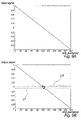
- FIG. 6B A preferred embodiment of the level controlled generator LCG amplitude-determining algorithm is illustrated graphically in FIG. 6B .
- This illustration comprises a horizontal axis corresponding to the absolute of the input amplitude and a vertical axis corresponding to the absolute of the outband signal amplitude, i.e. the output of the level controlled generator.
- the half of the range between the low threshold and the high threshold is shown as a horizontal dashed line HF.
- the amplitude of the input signal IS is shown as a dashed line and the amplitude OSL of the outband signal OBS is shown as a solid line.
- a first input signal amplitude range i.e.
- the outband signal amplitude is controlled as described above simply by adding a safe offset SO to the value of the input signal.
- the output signal OS at the sample times is either the safe offset SO or the twice of the input signal amplitude plus the safe offset value.
- the outband signal amplitude is smoothly decreased by determining it as the difference between a predetermined value, e.g. equal to the middle level value, and the input signal amplitude.
- the outband signal amplitude within this second input amplitude range the outband signal amplitude, thus, decreases in order to not get clipped at the maximum amplitude level.
- the outband signal amplitude For a third input signal amplitude range, i.e. input amplitudes between the middle level ML and maximum, the outband signal amplitude is steady at zero, i.e. the outband signal is switched off. Within this third amplitude range the input signal is, thus, not regulated in this specific embodiment of the present invention.
- the effect of the level controlled generator LCG of FIG. 6A for a silent signal as illustrated in FIG. 5B is exactly like for the embodiment of FIG. 5A .
- the outband signal amplitude takes the value of the safe offset SO shown in FIG. 6B .
- the output signal OS established by summing together the silent input signal IS with the outband signal OBS thus, becomes the same as in FIG. 5C , where the signal is outside the problematic range at every sample time.
- FIG. 5D of pulse width modulating the output signal OS of FIG. 5C also applies to this situation. None of the pulses are too narrow.
- FIG. 6C illustrates a different input signal IS, equal to the signal illustrated in FIG. 5E . It sweeps from a value above the high threshold HT across zero to a value below the low threshold LT.
- FIG. 6D illustrates the output signal OS resulting from summing together the input signal of FIG. 6C with an outband signal established according to the algorithm illustrated by FIG. 6B .
- the outband signal actually causes all of the input signal amplitudes within the problematic range to be pushed outside it, but nevertheless also causes a couple of good input signal amplitudes to be moved into the problematic range.
- a result of pulse width modulating the output signal is shown in FIG. 6E . As seen, two of the pulses marked with asterisks are narrower than minimum pulse width.
- FIGS. 7A to 7I illustrate the effect of the level controlled generator LCG generated outband signal OBS of a preferred embodiment of the present invention.
- an input signal IS is shown.
- the horizontal axis corresponds to time or samples, whereas the vertical axis corresponds to signal amplitude.
- FIG. 7A further comprises dashed lines indicating the low level LL and middle level ML amplitudes corresponding to FIG. 6B .
- FIG. 7B comprises a possible outband signal OBS established from the input signal of FIG. 7A on the basis of an algorithm in principle corresponding to the one shown in FIG. 6B .
- the input signal IS is above the middle level ML and thus, according to the algorithm of FIG. 6B , the outband signal in FIG. 7B is kept at zero.
- the algorithm of FIG. 6B causes the outband signal to build up, e.g. with an amplitude being the difference between the middle level ML or another fixed level and the input signal IS.
- the algorithm causes the amplitude of the outband signal OBS to track the input signal amplitude at an offset, e.g. a safe offset SO.
- FIG. 7C illustrates a possible output signal OS established by summing together the input signal IS of FIG. 7A and the outband signal OBS of FIG. 7B .
- the illustration comprises dashed lines indicating the high threshold HT and the low threshold LT.
- the output signal equals the input signal through the first stage, where the input signal is above the middle level ML.
- the oscillation builds up until the lower amplitude peaks are below the low threshold LT. From that time the lower amplitude peaks stays just below the low threshold LT while the higher amplitude peaks decrease with the signal until just above the high threshold HT. From there, the opposite behaviour is seen for the rest of the signal.
- the outband signal OBS should, preferably, have a mean value of zero in order not to disturb the utility signal. Thereby, it is achieved that the output signal of FIG. 7C render as the input signal in FIG. 7A when processed by a low pass filter. Furthermore, it may be seen that no peaks, i.e. samples when the signal is used for e.g. a PWM amplifier, are within the problematic range around the time where the input signal crosses zero.
- the output signal comprises altogether six samples within the problematic area at the times where the outband signal fades in or out. The distortion established by these samples is, however, less significant as the higher input signal level at that time causes a significantly higher signal/error-ratio.
- FIGS. 7D to 7I correspond to FIGS. 4A to 4F but regarding the embodiment of FIG. 6A instead of an empty amplitude distribution filter ADF.
- the input signal IS used for establishing the FIGS. 7D to 7I is a 1 kHz sine wave.
- FIG. 7D is a three-dimensional presentation of the output level distribution, indicated by shades of grey, for different input peak levels at the vertical axis and different output levels at the horizontal axis. Darker shades indicate a higher concentration of a specific output level within an output signal established from an input signal with a specific input peak level.
- FIGS. 7E to 7I comprise sectional views of the plot in FIG. 7D for five specific input signal peak levels.
- FIG. 7E comprises a sectional view at input peak level 0, FIG. 7F at input peak level 0.25, FIG. 7G at input peak level 0.5, FIG. 7H at input peak level 0.75 and FIG. 7I at input peak level 1.
- the output level distribution is zero within the problematic range between the low threshold and high thresholds, in this example approximately ⁇ 0.05 and 0.05. This is because the input signal at these levels never becomes above the low level LL and, thus, never causes the outband signal OBS to decrease, cf FIG. 6B .
- FIG. 8A illustrates an alternative embodiment of the amplitude distribution filter ADF of the present invention. It comprises an input signal IS and an output signal OS. The input signal is processed by a mapping means MM in order to establish the output signal OS.
- the embodiment furthermore, comprises a loop filter LF as in the embodiment of FIG. 6A .
- This loop filter is coupled in the same way as with the former embodiment and serves the same purpose, namely noise shaping of errors or noise injected to the forward path subsequent to the summing point 81 .
- the present embodiment also in a preferred embodiment comprises a quantizing means QZ but also embodiments without a separate quantizing means are within the scope of the present invention, hence the dashed outline.
- the mapping means MM maps any input level within the one or more problematic ranges to levels outside the problematic ranges. To levels already outside the problematic ranges nothing is done.
- the mapping means may be kinds of hard limiters or any other means more or less intelligent that facilitate clearance of a specific amplitude range.
- FIGS. 8B and 8C A possible effect of such a mapping means MM is shown by FIGS. 8B and 8C .
- FIG. 8B comprises an example input signal IS sweeping with time from a high amplitude across zero and a problematic range between a high threshold HT and a low threshold LT to a low amplitude.
- FIG. 8C illustrates a possible output 83 of a mapping means MM when fed with the input signal of FIG. 8B .
- the effect of the mapping means shown in FIG. 8C is for a stand-alone mapping means, i.e. without any feedback compensation or noise-shaping.
- the mapping means keeps the output signal 83 at that value, until the input signal decreases below zero.
- the mapping means maintains an output level of a little below the low threshold LT until the input signal also decreases below that value and the mapping means has its output 83 follow the input signal.
- the noise shaping feedback is applied by means of the loop filter LF.
- This filter may comprise the same characteristics as the loop filter in FIG. 6A , i.e. a low-pass IIR filter with a corner frequency at the top of the desired utility band, e.g. 20 kHz, and a large gain within the utility band.
- the quantizing means QZ may be added when any subsequent stages are not able to exploit the amplitude resolution of the input signal. Quantizing the signal before mapping it may ease the implementation of the mapping means considerably. Furthermore, by placing the quantizing means within the forward path being noise-shaped quantizing errors are rejected. By placing the quantizing means QZ within the noise shaping loop instead of subsequently to the amplitude distribution filter ADF, as it is also possible, the errors established by the quantizing means QZ are also noise shaped.
- FIGS. 9A to 9H illustrate possible effects of the embodiment of FIG. 8A .
- FIG. 9A comprises a possible input signal sweeping with time from its maximum level 1 to its minimum level ⁇ 1.
- FIG. 9B illustrates a possible output signal OS established by the embodiment illustrated in FIG. 8A , i.e. the combined mapping means MM and loop filter LF.
- the mapping means MM has caused the output signal to comprise no peak amplitudes within the range between the low threshold LT and high threshold HT.
- the oscillating nature of the output signal around the time where the input signal crosses zero, as opposed to the straightforward mapping shown in FIG. 8C is caused by the noise-shaping loop.
- FIGS. 9C to 9H correspond in type to the FIGS. 4A to 4F and 7 D to 7 I but are established by inputting a 1 kHz sine wave to the embodiment of FIG. 8A .
- the output level distribution is zero within the problematic range for any input peak level, i.e. no pulses of less than the minimum pulse width ever occur when applying the present embodiment to a PWM amplifier.
- FIG. 9D illustrating the output level distribution for a zero input signal, i.e. when idling, a certain concentration of output levels below and above the low and high thresholds exists. This is due to the noise shaping mechanism causing several different amplitude levels to be mapped to instead of just the threshold levels.
- FIG. 10 illustrates a preferred embodiment of the amplitude distribution filter ADF of the present invention. It comprises an input signal IS and an output signal OS. Furthermore, it comprises the elements of both the embodiment of FIG. 6A and the embodiment of FIG. 8A , i.e. a level controlled generator LCG adding an outband signal OBS to the input signal, a mapping means MM mapping signal level within certain ranges to certain different levels, and a loop filter LF, which in virtue of its location performs noise shaping.
- LCG level controlled generator
- OBS outband signal
- a mapping means MM mapping signal level within certain ranges to certain different levels
- a loop filter LF which in virtue of its location performs noise shaping.
- the addition of the outband signal to the input signal causes the input signal, at times with an amplitude close to zero, to be oscillating around the problematic range but, nevertheless, sometimes causes amplitudes within the problematic range to occur at other times.
- this composite signal comprising the outband signal and the input signal to be processed by the mapping means MM, it is ensured that no output signal levels within the problematic range occur, i.e. the output level distribution is zero between the low and high thresholds.
- the distortion injected by the mapping means is less than when the signal is not pre-processed by adding the outband signal as the outband signal causes far less samples to be mapped and also causes the times where mappings are required to be moved farther away from the input signal zero crossings.
- FIGS. 11A to 11C illustrate how the embodiment of FIG. 10 may affect a possible input signal.
- a possible input signal IS is shown in FIG. 11A together with dashed lines indicating the low level LL and middle level ML used for establishing the outband signal according to the algorithm of FIG. 6B .
- a corresponding outband signal OBS is shown in FIG. 11B .
- FIG. 11C illustrates a possible output signal OS established by the embodiment illustrated in FIG. 10 and on the basis of the input signal of FIG. 11A and the outband signal of FIG. 11B .
- FIG. 11C furthermore, comprises dashed lines indicating a low threshold LT and a high threshold HT.
- FIGS. 11D to 11I illustrate examples of the output signal level distribution that may result from the embodiment of FIG. 10 .
- FIG. 11D to 11I correspond in type to e.g. the FIGS. 9C to 9H but are established by inputting a 1 kHz sine wave to the embodiment of FIG. 10 .
- the output level distribution is zero within the problematic range for any input peak level, i.e. no pulses of less than the minimum pulse width ever occur when applying the present embodiment to a PWM amplifier.
- FIGS. 12 and 13 illustrate the relative noise floor, i.e. distortion and errors, which is comprised by the output signal by using the amplitude distribution filter embodiments of FIGS. 8A and 10 , respectively.
- the horizontal axes correspond to the absolute input level, i.e. 0 to 1 for the examples given above.
- the vertical axes correspond to the relative noise floor of the output signal.
- FIGS. 14A to 14D illustrate an alternative embodiment of the present invention.
- FIG. 14A is identical to FIG. 6A and comprises a level controlled generator establishing an outband signal OBS on the basis of an input signal IS and a loop filter LF acting as a noise shaper.
- FIG. 14B is identical to FIG. 5B and shows an empty input signal IS and low threshold LT and high threshold HT.
- FIG. 14C illustrates a possible output signal OS established by the embodiment of FIG. 14A . As the input signal IS is empty, the output signal OS of FIG. 14C also corresponds to the outband signal OBS added by the summing point 142 . Any preferences and characteristics of the outband signal mentioned above, e.g. regarding FIG.
- the outband signal of the present embodiment is preferably of a frequency rate a quarter of the rate at which the output signal is sampled in subsequent stages, e.g. in a subsequent pulse width modulator or digital amplifier. If, for example, the switching rate in a subsequent PWM amplifier is 384 kHz, the rate of a preferred outband signal would be 96 kHz. Thereby, it is possible as shown in FIG. 14C to have every second sample value to be zero for an empty input signal.
- the present example assumes a problematic range, e.g. due to non-linear processing in subsequent stages between the low threshold LT and high threshold HT.
- the level of exact zero is in fact not typically problematic.
- the problematic range may as well be divided into a range from the low threshold LT to, but not including, zero and a range from, but not including, zero to the high threshold HT. In such a system the embodiment of FIG. 14C may cause significant power savings.
- FIGS. 15A to 15C illustrate how the embodiment of FIG. 14A may process an example input signal not being zero.
- FIG. 15A illustrates a possible input signal IS, sweeping from 1 to ⁇ 1. It also illustrates possible low level LL and middle level ML of a possible level controlled outband signal algorithm as, e.g., the one illustrated in FIG. 6B .
- FIG. 15B illustrates a possible outband signal OBS established by the embodiment of FIG. 14A .
- the preferred sample values are shown by dots.
- FIG. 14C illustrates a possible output signal OS established by summing together the signals of FIGS. 14A and 14B and applying noise shaping by means of the loop filter LF.
- the preferred sample values are shown by dots.
- the low threshold LT and high threshold HT are shown.
- FIGS. 15D to 15I illustrate examples of the output signal level distribution that may result from the embodiment of FIG. 14A .
- FIG. 15D to 15I correspond in type to, e.g., the FIGS. 9C to 9H but are established by inputting a 1 kHz sine wave to the embodiment of FIG. 14A .
- FIGS. 15D and 15E only output levels of zero and safe offsets to either side of zero occur.
- FIGS. 15F to 15I and, e.g., by comparison with FIGS. 7F to 7I the concentration of occurrences of levels within the problematic range and, thus, pulses of less than the minimum pulse width if used for a PWM amplifier is greater than with the embodiment of FIG. 6A .
- FIGS. 16A to 16C illustrate yet an alternative embodiment of the present invention.
- FIG. 16A is identical to FIG. 8A and comprises an input signal being processed by an optional quantizing means QZ, a mapping means MM and a loop filter LF.
- the mapping means MM of the present embodiment maps values within the problematic range to zero instead of outside the problematic range. This is illustrated in FIGS. 16B and 16C .
- FIG. 16B illustrates a possible input signal IS and the problematic range is indicated by low threshold LT and high threshold HT.
- FIG. 16C illustrates the working of the mapping means MM by showing what would be the output 163 of the mapping means MM if the loop filter LF and feedback path were omitted. As seen from FIG. 16C the output 163 is mapped to the zero level when the input decreases below a value just above the high threshold HT and stays at zero until the input decreases below a value just below a low threshold LT.
- the quantizing means QZ may be added when any subsequent stages are not able to exploit the amplitude resolution of the input signal. Quantizing the signal before mapping it may ease the implementation of the mapping means considerably. Furthermore, by placing the quantizing means within the forward path being noise-shaped results in the rejection of quantizing errors.
- FIGS. 17A to 17H illustrate possible effects of the embodiment of FIG. 16A .
- FIG. 17A comprises a possible input signal sweeping with time from its maximum level 1 to its minimum level ⁇ 1.
- FIG. 17B illustrates a possible output signal OS established by the embodiment illustrated in FIG. 16A , i.e. the combined mapping means MM and loop filter LF.
- the mapping means MM has caused the output signal to comprise several preferred sample points, indicated by dots, at the zero level but no points at other levels within the problematic range, i.e. the range between the low threshold LT and high threshold HT.
- the noise-shaping loop causes a few points to be pushed outside the problematic range instead of being mapped to zero.
- FIGS. 17C to 17H correspond in type to, e.g., the FIGS. 9C to 9H but are established by inputting a 1 kHz sine wave to the embodiment of FIG. 16A .
- the output level distribution has a high concentration at the output level of zero all input peak levels.
- the output level distribution is zero for all other values within the range between the low threshold and high threshold, i.e. no pulses of less than the minimum pulse width, except for zero, ever occur when applying the present embodiment to a PWM amplifier.
- FIG. 17D illustrating the output level distribution for a zero input signal, i.e. when idling, a certain concentration of output levels below and above the low and high thresholds exists.
- FIG. 18 illustrates a preferred embodiment of the amplitude distribution filter ADF of the present invention. It comprises an input signal IS and an output signal OS. Furthermore, it comprises the elements of both the embodiment of FIG. 14A and the embodiment of FIG. 16A , i.e. a level controlled generator LCG adding an outband signal OBS to the input signal, a mapping means MM mapping signal level within certain ranges to zero and a loop filter LF, which in virtue of its location performs noise shaping.
- LCG level controlled generator
- OBS outband signal
- a mapping means MM mapping signal level within certain ranges to zero
- a loop filter LF which in virtue of its location performs noise shaping.
- the addition of the outband signal to the input signal causes the input signal, at times with an amplitude close to zero, to be oscillating around the problematic range but, nevertheless, sometimes causes amplitudes within the problematic range to occur at other times. Furthermore, for empty input signals it causes every second preferred sample point to be at a level of zero.
- this composite signal comprising the outband signal and the input signal to be processed by the mapping means MM it is ensured that no output signal levels within the problematic range, except for zero, occur, i.e. the output level distribution is zero between the low and high thresholds except for the output level zero, which has a high concentration.
- the distortion injected by the mapping means is reduced compared to an embodiment not proving an additive outband signal, as the outband signal causes less samples to require mapping and also causes the situations where mapping are required to be moved farther away from the input signal zero level crossings.
- the signal/error-ratio is thus improved for small signals compared to the signal/error ratio of, e.g., the embodiment of FIG. 16A .
- FIGS. 19A to 19C illustrate how the embodiment of FIG. 18 may affect a possible input signal.
- a possible input signal IS is shown in FIG. 19A together with dashed lines indicating the low level LL and middle level ML used for establishing the outband signal according to the algorithm of FIG. 6B .
- a corresponding outband signal OBS is shown in FIG. 19B with preferred sample points indicated by dots.
- FIG. 19C illustrates a possible output signal OS established by the embodiment illustrated in FIG. 18 and on the basis of the input signal of FIG. 19A and the outband signal of FIG. 19B . Furthermore, FIG. 19C comprises dashed lines indicating a low threshold LT and a high threshold HT and dots indicating preferred sample points. As it can be seen, it is possible by means of the embodiment of FIG. 18 to establish an output signal comprising only sample values outside the problematic range between the low and high thresholds and sample values with a level of zero. Thereby, it is ensured that a possible subsequent PWM amplifier is not required to establish pulses with less than a minimum pulse width.
- FIGS. 19D to 19I illustrate examples of the output signal level distribution that may result from the embodiment of FIG. 18 .
- FIGS. 19D to 19I correspond in type to, e.g., the FIGS. 9C to 9H , but are established by inputting a 1 kHz sine wave to the embodiment of FIG. 18 .
- the output level distribution is zero within the problematic range for any input peak level except for the output level of zero, which represents a high concentration.
- FIG. 18 combining the embodiments of FIGS. 14A and 16A improves the performance of each of these.
- FIGS. 20 and 21 illustrate the relative noise floor, i.e. distortion and errors that may be comprised by an output signal when using the amplitude distribution filter ADF embodiments of FIGS. 16A and 18 , respectively.
- the horizontal axes correspond to the absolute input level, i.e. 0 to 1 for the examples given above.
- the vertical axes correspond to the relative noise floor of the output signal.
- the outband signal of the embodiments of FIGS. 14A and 18 should preferably cause a significant amount of zeroes to be sampled by subsequent stages.
- the amount of zeroes to be sampled should, preferably, be less than the half of the samples and, most preferably, the half of the samples, e.g. every second sample.
- non-periodic signals e.g. white noise, may be used for outband signals but should also be established in a way ensuring a considerable amount of zeroes to be sampled.
- FIG. 22A illustrates a further, preferred embodiment of the present invention. Like the embodiment of FIG. 6A it comprises an input signal IS, which is turned into an output signal OS by adding an outband signal OBS to it by means of a summing point 222 .
- the outband signal of the embodiment of FIG. 22A is established by means of a level controlled generator LCG.
- the level controlled generator is controlled at least partly by an input connected to the input signal.
- An outband signal that is amplitude controlled by the input signal may, thus, be established.
- the particular characteristics of the outband signal e.g. waveform, frequency, etc., may be freely chosen or determined by other parameters as with the embodiment of FIG. 5A , and need not to be controlled by the input signal.
- the level controlled generator may, e.g., be implemented as a signal generator with voltage controlled gain.
- the embodiment of FIG. 22A further comprises a loop filter LF.
- the loop filter is in the embodiment of FIG. 6A located in the feedback path from the output signal OS in such a way that is processes the difference between the output signal OS and the input signal IS and the output of the loop filter LF is subtracted from the input signal IS by means of a summing point 221 .
- the loop filter LF as described regarding the embodiment of FIG. 6A serves as a noise shaper to distortion and errors introduced to the signal forward path.
- Such preferred loop filter implementation may comprise a low-pass IIR filter, i.e. infinite impulse response filter, with a corner frequency at the top of the desired utility band, e.g. 20 kHz, and a large gain within the utility band.
- any rules or algorithms for determining the outband signal amplitude on the basis of the input signal may be implemented.
- the choice of algorithm or rule to implement may be restricted by the system dynamics, in particular typically requiring the output signal OS to not exceed the maximum level of the input signal, e.g. 1, and thus requiring the sum of the input signal IS and the outband signal OBS to not exceed e.g. 1.
- the subsequent processing means comprises certain kinds of three-level PWM amplifiers.
- An example of such an amplifier typically comprises an H-bridge system or a bridge-tied load system, where a single power supply with +VCC and GND by means of typically 4 switches are able to establish three levels, +VCC, GND and ⁇ VCC over the load.
- positive input signal values are represented by means of pulses of level +VCC established by a first set of 2 switches, whereas negative input signal values are represented by means of pulses of level ⁇ VCC established by a second set of 2 switches. Between the pulses the level is GND.
- the load should be coupled between the outputs of the two sets of switches, instead of as typically between one set of switches and the ground-plane. Hence, if the input signal is, e.g., a positive DC-signal only the first set of switches operates, and vice versa.
- the level controlled generator LCG of FIG. 22A may comprises level control algorithms that is not possible to use with the embodiment of FIG. 6A .
- An example of such a preferred algorithm is illustrated graphically in FIG. 22B .
- This illustration comprises a horizontal axis corresponding to the absolute of the input amplitude and a vertical axis corresponding to the absolute of the outband signal amplitude, i.e. the output of the level controlled generator.
- the half of the range between the low threshold and the high threshold, i.e. typically the range from zero level to the high threshold, is shown as a horizontal dashed line HT.
- the amplitude of the input signal IS is shown as a dashed line and the amplitude OSL of the outband signal OBS is shown as a solid line.
- the outband signal amplitude is for all input levels determined by adding a safe offset SO to the value of the input signal. Thereby, for a zero input, the outband signal amplitude stays just outside the range between the thresholds at the sample times, provided that the frequency of the outband signal is half the frequency of the sampling performed in subsequent stages. For a non-zero input, the outband signal amplitude alternates between the safe offset value SO and values considerably higher than the input signal amplitude.
- this implementation requires far better dynamic parameters than needed to provide for the input signal itself, and such dynamics are just what is provided by the above described PWM amplifier.
- the effect of the level controlled generator LCG of FIG. 22A for a silent signal as illustrated in FIG. 5B is exactly like for the embodiment of FIG. 5A .
- the outband signal amplitude takes the value of the safe offset SO shown in FIG. 22B .
- the output signal OS established by summing together the silent input signal IS with the outband signal OBS thus, becomes the same as in FIG. 5C , where the signal is outside the problematic range at every sample time.
- FIG. 5D of pulse width modulating the output signal OS of FIG. 5C also applies to this situation. None of the pulses are too narrow.
- FIG. 22C illustrates a different input signal IS, first constant at approximately ⁇ 0.8, then ramping to approximately 0.8 where it stays.
- the horizontal axis corresponds to time, and vertical strokes indicate the switch periods.
- the vertical axis corresponds to the signal amplitude.
- Horizontal lines are provided corresponding to the low threshold LT and high threshold HT.
- the diagram further comprises a possible output signal OS established by means of the embodiment of FIG. 22A on the basis of the input signal IS and the level control algorithm of FIG. 22B .
- the output signal alternates between a positive value corresponding to the safe offset SO, just above the high threshold HT, and a negative value corresponding to twice the input signal level minus the safe offset SO.
- the output signal When the input signal level is positive, the output signal alternates between a negative value corresponding to the negative of the safe offset SO, just below the low threshold LT, and a positive value corresponding to twice the input signal level plus the safe offset SO. Hence, when the input signal approaches the maximum amplitude of 1, the output signal approaches twice that amplitude, i.e. 2 in the present example.
- the algorithm of FIG. 22B By using the algorithm of FIG. 22B is obtained that no output signal samples is between the low threshold and high threshold.
- FIG. 22C furthermore comprises examples of a PWM signal established from the output signal OS of FIG. 22C .
- Strokes on the horizontal axes indicate the PWM periods.
- the PWM signal in this example is a three level signal comprising a first signal PWMA and a second signal PWMB.
- the signals are established in such a way that positive output signal levels are represented by pulses in the first signal PWMA, and negative output signal levels are represented by pulses in the second signal PWMB.
- signal represented by the PWM signal alternates between negative and positive values, as the output signal in FIG. 22C , there will always be an empty PWM period between each pulse in each signal. As described above these empty periods may be used for increasing the pulse widths of the active periods.
- the present embodiment of the invention furthermore ensures that the two PWM signal parts PWMA and PWMB preferably never, and at least less often, comprise pulses at the same times, by ensuring narrow, yet not too narrow, pulses in one signal part, e.g. PWMA, while establishing broad pulses in the other signal part, e.g. PWMB.
- FIGS. 23A and 23B illustrate relationships between the output and the input of a process being non-linear for inputs within certain ranges. They relate to FIGS. 3A and 3B illustrating the ideal relationship and a relationship comprising a non-linear processing range in the middle of the full level range.
- FIG. 23A comprises an example of a relationship 231 comprising several amplitude ranges in which the output is distorted, whereof also some of these obviously does not comprise the zero level.
- the ranges comprise values between a first low threshold LT 1 and a first high threshold HT 1 , between second low and high threshold LT 2 , HT 2 , and between third low and high thresholds LT 3 , HT 3 .
- FIG. 23B illustrates an output/input relationship 232 where the amplitude range with non-linear relationship is dynamically positioned within the input level range.
- the range extends from a dynamically positioned low threshold DLT to a dynamically positioned high threshold DHT. It is noted that both the extent of the range as well as the position may in some embodiments be dynamically adapted. It is furthermore noted that a possible output/input relationship may simultaneously comprise several dynamically positioned ranges or a combination of fixed and dynamically positioned ranges, and that also the number of ranges may be dynamically changed, e.g. when two or more ranges partly or fully coincide, or due to any other reason.
- FIG. 24 An example of an application where dynamically positioned problematic amplitude ranges as described above regarding FIG. 23B may be advantageously utilized is given in FIG. 24 .
- MCS multi-channel PWM modulator system
- Such a system may, e.g., be used for pulse width modulating several audio channels, e.g. 6 channels, and may advantageously be implemented in a single integrated circuit.
- One of several issues to consider when implementing a system in an integrated circuit is the use of external chip connectors, as the number of these significantly impacts the cost of the integrated circuit, i.e. production and materials.
- a possible solution to this problem is to combine the multiple audio channels into a fewer number of physical conductors.
- the system comprises 6 audio channels it may be possible by means of a proper multiplexing algorithm, compression algorithm, etc., to combine the information of these into, e.g., 2 or 4 physical wires.
- FIG. 24 is shown two signals entering the multi-channel PWM modulator system MCS. These signals may each require more than one physical connector, but use together preferably less than 6 connectors.
- the combined channels signal is split into a signal for each of the 6 individual channels by a signal splitter 121 .
- each of the 6 channels may enter the multi-channel system MCS by its own physical connector.
- Each of the 6 channels are provided to a pulse width modulating system PWMS 1 , PWMS 2 , . . .
- modulator output signals MOS 1 , etc. which are pulse width modulated representations for the input signal IS 1 , etc., are again combined into preferably less than 6 physically wired signals by means of a signal combiner 123 .
- FIG. 24 further comprises a signal splitter 124 for dividing the combined modulator output signal into a signal for each channel outside the integrated circuit comprising the multi-channel pulse width modulator system MCS.
- Each of these pulse width modulated output channels may then be fed to, e.g., separate amplifiers AMP 1 , . . . , AMP 6 , preferably switch-mode amplifiers.
- the combined modulator output signal may be fed directly to each of the subsequent, e.g., amplifiers by bypassing the signal splitter 124 .
- the subsequent stage, e.g. amplifier should then be adapted to retrieve from the combined signal only the relevant channel.
- a further reason for desiring non-concurrent pulse flanks is the probability of establishing cross-talk when, e.g., the amplifiers AMP 1 , . . . , AMP 6 are operated from the same power supply. By ensuring that the switches in different amplifiers are never required to switch simultaneously, the problem of cross-talk may be reduced.
- Guaranteeing or at least increasing the probability of non-concurrent flanks in a multi-channel system is thus desired, and one way in which this may be ensured is, within the example embodiment of FIG. 24 , by dynamically adapting the problematic amplitude ranges of some of the pulse width modulator systems PWMS 1 , . . . , PWMS 6 according to the intermediate output signal amplitudes of other pulse width modulator systems PWMS 1 , . . . , PWMS 6 .
- Such dynamically adapting the problematic amplitude ranges may e.g. be performed be a control unit 122 connected with each pulse width modulator system PWMS 1 , . . . , PWMS 6 by means of two-way external control signals ECS 1 , etc. Thereby the control unit 122 may continuously obtain information of the currently processed input values or intermediate output values, and adaptively establish control information accordingly.
Applications Claiming Priority (1)
| Application Number | Priority Date | Filing Date | Title |
|---|---|---|---|
| PCT/DK2004/000376 WO2005117253A1 (fr) | 2004-05-28 | 2004-05-28 | Systeme de modulateur d'impulsions en duree |
Publications (2)
| Publication Number | Publication Date |
|---|---|
| US20080278253A1 US20080278253A1 (en) | 2008-11-13 |
| US7728689B2 true US7728689B2 (en) | 2010-06-01 |
Family
ID=34957542
Family Applications (2)
| Application Number | Title | Priority Date | Filing Date |
|---|---|---|---|
| US11/596,606 Expired - Fee Related US7728689B2 (en) | 2004-05-28 | 2004-05-28 | Pulse width modulator system |
| US11/596,642 Abandoned US20080211594A1 (en) | 2004-05-28 | 2005-05-30 | Multi-Channel Pulse Modulator System |
Family Applications After (1)
| Application Number | Title | Priority Date | Filing Date |
|---|---|---|---|
| US11/596,642 Abandoned US20080211594A1 (en) | 2004-05-28 | 2005-05-30 | Multi-Channel Pulse Modulator System |
Country Status (5)
| Country | Link |
|---|---|
| US (2) | US7728689B2 (fr) |
| EP (2) | EP1751855B1 (fr) |
| AT (2) | ATE387750T1 (fr) |
| DE (2) | DE602004012165T2 (fr) |
| WO (2) | WO2005117253A1 (fr) |
Families Citing this family (7)
| Publication number | Priority date | Publication date | Assignee | Title |
|---|---|---|---|---|
| ATE387750T1 (de) * | 2004-05-28 | 2008-03-15 | Tc Electronic As | Impulsbreitenmodulatorsystem |
| GB2449591B (en) | 2005-01-17 | 2009-03-18 | Wolfson Microelectronics Plc | Pulse width modulator quantisation circuit |
| US7613920B2 (en) | 2005-08-22 | 2009-11-03 | Alcatel Lucent | Mechanism to avoid expensive double-encryption in mobile networks |
| US7720170B2 (en) * | 2005-12-13 | 2010-05-18 | Awq Consulting Inc. | Low emission signal generator and distributor system |
| WO2013088173A1 (fr) * | 2011-12-14 | 2013-06-20 | Wolfson Microelectronics Plc | Transfert de données |
| GB2497566A (en) * | 2011-12-14 | 2013-06-19 | Wolfson Microelectronics Plc | Simultaneous transmission of a plurality of audio data streams via a single communication link |
| DE102022104868B4 (de) | 2022-03-02 | 2024-05-02 | Webasto SE | Anordnung zum Betreiben einer elektrischen Komponente in einem Fahrzeug |
Citations (18)
| Publication number | Priority date | Publication date | Assignee | Title |
|---|---|---|---|---|
| JPS5521577A (en) | 1978-08-03 | 1980-02-15 | Nippon Kokan Kk <Nkk> | Method of cooling material loading device at the top of blast furnace |
| US4240036A (en) | 1979-04-13 | 1980-12-16 | General Electric Company | Linearized three-state switching amplifier |
| LU84520A1 (fr) | 1982-12-10 | 1984-10-22 | Wurth Paul Sa | Dispositif de refroidissement d'une installation de chargement d'un four a cuve |
| US5252063A (en) | 1991-06-12 | 1993-10-12 | Paul Wurth S.A. | Cooling device for the distribution chute of an installation for charging a shaft furnace |
| US5617058A (en) | 1995-11-13 | 1997-04-01 | Apogee Technology, Inc. | Digital signal processing for linearization of small input signals to a tri-state power switch |
| US6028944A (en) | 1997-03-04 | 2000-02-22 | Compaq Computer Corporation | Signal processing apparatus with selective power amplification |
| US6031481A (en) | 1991-02-22 | 2000-02-29 | B & W Loudspeakers Ltd. | Analogue and digital converters |
| US6107876A (en) | 1999-04-13 | 2000-08-22 | Ravisent Technologies, Inc. | Digital input switching audio power amplifier |
| US6320465B1 (en) | 1999-04-27 | 2001-11-20 | Stmicroelectronics S.R.L. | Constant duty-cycle limiting of analog input signal swing in a class-D amplifier |
| EP1178388A1 (fr) | 2000-08-04 | 2002-02-06 | STMicroelectronics S.r.l. | Convertisseur MIC/MID avec amplificateur MID de puissance |
| US6429737B1 (en) | 2000-07-06 | 2002-08-06 | Stmicroelectronics, Inc. | Method and apparatus for multi-channel digital amplification |
| US6538504B1 (en) | 2000-05-19 | 2003-03-25 | Jam Technologies, Llc | Switching amplifier crossover distortion reduction technique |
| US20030122692A1 (en) | 2002-01-02 | 2003-07-03 | Roeckner William J. | Method and apparatus for generating a pulse width modulated signal |
| US6665338B1 (en) | 2000-01-05 | 2003-12-16 | Motorola, Inc. | Circuitry for converting a sampled digital signal to a naturally sampled digital signal and method therefor |
| US6671329B1 (en) | 1998-12-14 | 2003-12-30 | Siemens Aktiengesellschaft | Power amplifier |
| WO2004105242A2 (fr) | 2003-05-20 | 2004-12-02 | Tc Electronics A/S | Procede pour estimer une intersection entre au moins deux representations continues de signaux |
| WO2005004330A1 (fr) | 2003-07-07 | 2005-01-13 | Tc Electronic A/S | Procede permettant d'etablir une representation de signaux de sortie modules par pwm |
| US6970051B2 (en) * | 2003-12-08 | 2005-11-29 | Harris Corporation | Pulse width modulator circuit having negative bias |
Family Cites Families (13)
| Publication number | Priority date | Publication date | Assignee | Title |
|---|---|---|---|---|
| JPS5582596A (en) * | 1978-12-18 | 1980-06-21 | Sony Corp | Head phone unit |
| US4345323A (en) * | 1980-01-07 | 1982-08-17 | Amp Incorporated | Pulse duration digital multiplexing system |
| DE3264600D1 (en) * | 1981-02-16 | 1985-08-14 | Bbc Brown Boveri & Cie | Method of amplifying an analog low-frequency signal using a switching amplifier and switching amplifier for carrying out said method |
| US4703471A (en) * | 1985-01-02 | 1987-10-27 | General Electric Company | Monolithically integrated electro-optical multiplexer/demultiplexer |
| JPS61171244A (ja) * | 1985-01-25 | 1986-08-01 | Nippon Signal Co Ltd:The | パルス幅変調波の合成方法 |
| US5956674A (en) * | 1995-12-01 | 1999-09-21 | Digital Theater Systems, Inc. | Multi-channel predictive subband audio coder using psychoacoustic adaptive bit allocation in frequency, time and over the multiple channels |
| CA2362104A1 (fr) * | 2000-10-30 | 2002-04-30 | Simon Fraser University | Methodes et systemes d'amplification de puissance a rendement eleve |
| US6593807B2 (en) * | 2000-12-21 | 2003-07-15 | William Harris Groves, Jr. | Digital amplifier with improved performance |
| US6552607B1 (en) * | 2001-11-12 | 2003-04-22 | Apogee Technology Inc. | Time division multiplexed PWM amplifier |
| US20040189502A1 (en) * | 2003-03-04 | 2004-09-30 | Lee Ying Lau | Multi-level pulse width modulation in digital system |
| US20040223545A1 (en) * | 2003-03-04 | 2004-11-11 | Lee Ying Lau | Multi-level pulse width modulation in digital system |
| DE10337782B4 (de) * | 2003-07-14 | 2007-03-01 | Micronas Gmbh | Methode und Schaltung zur effektiven Konvertierung von PCM-in PWM-Daten |
| ATE387750T1 (de) * | 2004-05-28 | 2008-03-15 | Tc Electronic As | Impulsbreitenmodulatorsystem |
-
2004
- 2004-05-28 AT AT04735195T patent/ATE387750T1/de not_active IP Right Cessation
- 2004-05-28 DE DE602004012165T patent/DE602004012165T2/de active Active
- 2004-05-28 US US11/596,606 patent/US7728689B2/en not_active Expired - Fee Related
- 2004-05-28 WO PCT/DK2004/000376 patent/WO2005117253A1/fr active IP Right Grant
- 2004-05-28 EP EP04735195A patent/EP1751855B1/fr not_active Not-in-force
-
2005
- 2005-05-30 EP EP05744247A patent/EP1751856B1/fr not_active Not-in-force
- 2005-05-30 AT AT05744247T patent/ATE421190T1/de not_active IP Right Cessation
- 2005-05-30 DE DE602005012384T patent/DE602005012384D1/de active Active
- 2005-05-30 US US11/596,642 patent/US20080211594A1/en not_active Abandoned
- 2005-05-30 WO PCT/DK2005/000358 patent/WO2005117382A2/fr active Application Filing
Patent Citations (19)
| Publication number | Priority date | Publication date | Assignee | Title |
|---|---|---|---|---|
| JPS5521577A (en) | 1978-08-03 | 1980-02-15 | Nippon Kokan Kk <Nkk> | Method of cooling material loading device at the top of blast furnace |
| US4240036A (en) | 1979-04-13 | 1980-12-16 | General Electric Company | Linearized three-state switching amplifier |
| LU84520A1 (fr) | 1982-12-10 | 1984-10-22 | Wurth Paul Sa | Dispositif de refroidissement d'une installation de chargement d'un four a cuve |
| US6031481A (en) | 1991-02-22 | 2000-02-29 | B & W Loudspeakers Ltd. | Analogue and digital converters |
| US5252063A (en) | 1991-06-12 | 1993-10-12 | Paul Wurth S.A. | Cooling device for the distribution chute of an installation for charging a shaft furnace |
| US5617058A (en) | 1995-11-13 | 1997-04-01 | Apogee Technology, Inc. | Digital signal processing for linearization of small input signals to a tri-state power switch |
| US6028944A (en) | 1997-03-04 | 2000-02-22 | Compaq Computer Corporation | Signal processing apparatus with selective power amplification |
| US6671329B1 (en) | 1998-12-14 | 2003-12-30 | Siemens Aktiengesellschaft | Power amplifier |
| US6107876A (en) | 1999-04-13 | 2000-08-22 | Ravisent Technologies, Inc. | Digital input switching audio power amplifier |
| US6320465B1 (en) | 1999-04-27 | 2001-11-20 | Stmicroelectronics S.R.L. | Constant duty-cycle limiting of analog input signal swing in a class-D amplifier |
| US6665338B1 (en) | 2000-01-05 | 2003-12-16 | Motorola, Inc. | Circuitry for converting a sampled digital signal to a naturally sampled digital signal and method therefor |
| US6538504B1 (en) | 2000-05-19 | 2003-03-25 | Jam Technologies, Llc | Switching amplifier crossover distortion reduction technique |
| US6429737B1 (en) | 2000-07-06 | 2002-08-06 | Stmicroelectronics, Inc. | Method and apparatus for multi-channel digital amplification |
| EP1178388A1 (fr) | 2000-08-04 | 2002-02-06 | STMicroelectronics S.r.l. | Convertisseur MIC/MID avec amplificateur MID de puissance |
| US20030122692A1 (en) | 2002-01-02 | 2003-07-03 | Roeckner William J. | Method and apparatus for generating a pulse width modulated signal |
| WO2004105242A2 (fr) | 2003-05-20 | 2004-12-02 | Tc Electronics A/S | Procede pour estimer une intersection entre au moins deux representations continues de signaux |
| WO2004105233A1 (fr) | 2003-05-20 | 2004-12-02 | Tc Electronic A/S | Procede permettant d'estimer une intersection entre au moins deux representations de signal continu |
| WO2005004330A1 (fr) | 2003-07-07 | 2005-01-13 | Tc Electronic A/S | Procede permettant d'etablir une representation de signaux de sortie modules par pwm |
| US6970051B2 (en) * | 2003-12-08 | 2005-11-29 | Harris Corporation | Pulse width modulator circuit having negative bias |
Non-Patent Citations (2)
| Title |
|---|
| European Search Report; EP08000266; May 8, 2008. |
| International Search Report; PCT/DK2004/000376; Dec. 3, 2004 (all references in search report listed above). |
Also Published As
| Publication number | Publication date |
|---|---|
| ATE421190T1 (de) | 2009-01-15 |
| EP1751856B1 (fr) | 2009-01-14 |
| US20080211594A1 (en) | 2008-09-04 |
| EP1751856A2 (fr) | 2007-02-14 |
| WO2005117382A2 (fr) | 2005-12-08 |
| ATE387750T1 (de) | 2008-03-15 |
| DE602004012165D1 (de) | 2008-04-10 |
| EP1751855B1 (fr) | 2008-02-27 |
| WO2005117382A3 (fr) | 2006-03-16 |
| EP1751855A1 (fr) | 2007-02-14 |
| US20080278253A1 (en) | 2008-11-13 |
| WO2005117253A1 (fr) | 2005-12-08 |
| DE602004012165T2 (de) | 2009-06-18 |
| DE602005012384D1 (de) | 2009-03-05 |
Similar Documents
| Publication | Publication Date | Title |
|---|---|---|
| JP5003134B2 (ja) | 増幅装置 | |
| EP2263355B1 (fr) | Modulateur numérique de haute résolution avec basculement entre des valeurs PWM ou PPM différentes | |
| US7057456B2 (en) | Class D amplifier | |
| US7276963B2 (en) | Switching power amplifier and method for amplifying a digital input signal | |
| KR101060359B1 (ko) | 펄스 폭 변조 증폭기 및 자동 이득 제어용 전원신호 제거장치와 방법 | |
| US7852150B1 (en) | Switching amplifier driven by a controlled power supply | |
| US8410845B2 (en) | Switching power amplifier and method of controlling the same | |
| US5559467A (en) | Digital, pulse width modulation audio power amplifier with noise and ripple shaping | |
| US7286008B2 (en) | Digital amplifier | |
| WO2007080741A1 (fr) | Dispositif d'amplification | |
| US7728689B2 (en) | Pulse width modulator system | |
| US20050054307A1 (en) | Signal processing circuit | |
| US6937175B1 (en) | Amplifier linearization using delta-sigma predistortion | |
| US7170360B2 (en) | Device and method for digital pulse width modulation | |
| EP1936801A1 (fr) | Système de modulateur de longueur d'impulsion | |
| US20040189502A1 (en) | Multi-level pulse width modulation in digital system |
Legal Events
| Date | Code | Title | Description |
|---|---|---|---|
| AS | Assignment |
Owner name: TC ELECTRONICS A/S, DENMARK Free format text: ASSIGNMENT OF ASSIGNORS INTEREST;ASSIGNORS:PEDERSEN, KIM RISHOJ;ARKNAES-PEDERSEN, LARS;REEL/FRAME:018916/0088;SIGNING DATES FROM 20061012 TO 20061130 Owner name: TC ELECTRONICS A/S,DENMARK Free format text: ASSIGNMENT OF ASSIGNORS INTEREST;ASSIGNORS:PEDERSEN, KIM RISHOJ;ARKNAES-PEDERSEN, LARS;SIGNING DATES FROM 20061012 TO 20061130;REEL/FRAME:018916/0088 |
|
| AS | Assignment |
Owner name: THE TC GROUP A/S, DENMARK Free format text: ASSIGNMENT OF ASSIGNORS INTEREST;ASSIGNOR:TC ELECTRONIC A/S;REEL/FRAME:021540/0687 Effective date: 20080813 Owner name: THE TC GROUP A/S,DENMARK Free format text: ASSIGNMENT OF ASSIGNORS INTEREST;ASSIGNOR:TC ELECTRONIC A/S;REEL/FRAME:021540/0687 Effective date: 20080813 |
|
| STCF | Information on status: patent grant |
Free format text: PATENTED CASE |
|
| FPAY | Fee payment |
Year of fee payment: 4 |
|
| FEPP | Fee payment procedure |
Free format text: PAT HOLDER NO LONGER CLAIMS SMALL ENTITY STATUS, ENTITY STATUS SET TO UNDISCOUNTED (ORIGINAL EVENT CODE: STOL); ENTITY STATUS OF PATENT OWNER: LARGE ENTITY |
|
| AS | Assignment |
Owner name: MUSIC GROUP IP LTD., VIRGIN ISLANDS, BRITISH Free format text: ASSIGNMENT OF ASSIGNORS INTEREST;ASSIGNOR:THE TC GROUP A/S;REEL/FRAME:039250/0315 Effective date: 20160701 |
|
| MAFP | Maintenance fee payment |
Free format text: PAYMENT OF MAINTENANCE FEE, 8TH YEAR, LARGE ENTITY (ORIGINAL EVENT CODE: M1552) Year of fee payment: 8 |
|
| FEPP | Fee payment procedure |
Free format text: MAINTENANCE FEE REMINDER MAILED (ORIGINAL EVENT CODE: REM.); ENTITY STATUS OF PATENT OWNER: LARGE ENTITY |
|
| LAPS | Lapse for failure to pay maintenance fees |
Free format text: PATENT EXPIRED FOR FAILURE TO PAY MAINTENANCE FEES (ORIGINAL EVENT CODE: EXP.); ENTITY STATUS OF PATENT OWNER: LARGE ENTITY |
|
| STCH | Information on status: patent discontinuation |
Free format text: PATENT EXPIRED DUE TO NONPAYMENT OF MAINTENANCE FEES UNDER 37 CFR 1.362 |
|
| FP | Lapsed due to failure to pay maintenance fee |
Effective date: 20220601 |