US7722437B2 - Manufacturing method of semiconductor integrated circuit device - Google Patents
Manufacturing method of semiconductor integrated circuit device Download PDFInfo
- Publication number
- US7722437B2 US7722437B2 US12/116,958 US11695808A US7722437B2 US 7722437 B2 US7722437 B2 US 7722437B2 US 11695808 A US11695808 A US 11695808A US 7722437 B2 US7722437 B2 US 7722437B2
- Authority
- US
- United States
- Prior art keywords
- dresser
- integrated circuit
- semiconductor integrated
- circuit device
- manufacturing
- Prior art date
- Legal status (The legal status is an assumption and is not a legal conclusion. Google has not performed a legal analysis and makes no representation as to the accuracy of the status listed.)
- Expired - Fee Related
Links
- 239000004065 semiconductor Substances 0.000 title claims abstract description 64
- 238000004519 manufacturing process Methods 0.000 title claims abstract description 61
- 238000005498 polishing Methods 0.000 claims abstract description 116
- 238000005299 abrasion Methods 0.000 claims abstract description 11
- 239000002002 slurry Substances 0.000 claims abstract description 9
- 238000006073 displacement reaction Methods 0.000 claims description 30
- 238000011282 treatment Methods 0.000 claims description 26
- VYPSYNLAJGMNEJ-UHFFFAOYSA-N Silicium dioxide Chemical compound O=[Si]=O VYPSYNLAJGMNEJ-UHFFFAOYSA-N 0.000 claims description 15
- 239000000126 substance Substances 0.000 claims description 14
- 229910052814 silicon oxide Inorganic materials 0.000 claims description 7
- 238000003825 pressing Methods 0.000 claims description 4
- 230000008859 change Effects 0.000 claims description 3
- 238000009413 insulation Methods 0.000 claims description 3
- 239000000470 constituent Substances 0.000 claims description 2
- 238000005259 measurement Methods 0.000 abstract description 9
- 239000003344 environmental pollutant Substances 0.000 abstract description 2
- 231100000719 pollutant Toxicity 0.000 abstract description 2
- 235000012431 wafers Nutrition 0.000 description 46
- 239000010410 layer Substances 0.000 description 23
- 238000000034 method Methods 0.000 description 19
- 230000008569 process Effects 0.000 description 12
- 230000007246 mechanism Effects 0.000 description 11
- 238000012545 processing Methods 0.000 description 11
- 230000009471 action Effects 0.000 description 10
- 239000000758 substrate Substances 0.000 description 10
- XUIMIQQOPSSXEZ-UHFFFAOYSA-N Silicon Chemical compound [Si] XUIMIQQOPSSXEZ-UHFFFAOYSA-N 0.000 description 8
- 229910052710 silicon Inorganic materials 0.000 description 8
- 239000010703 silicon Substances 0.000 description 8
- RYGMFSIKBFXOCR-UHFFFAOYSA-N Copper Chemical compound [Cu] RYGMFSIKBFXOCR-UHFFFAOYSA-N 0.000 description 5
- 229910052782 aluminium Inorganic materials 0.000 description 5
- 229910052802 copper Inorganic materials 0.000 description 5
- 239000010949 copper Substances 0.000 description 5
- 229910052751 metal Inorganic materials 0.000 description 5
- 239000002184 metal Substances 0.000 description 5
- XAGFODPZIPBFFR-UHFFFAOYSA-N aluminium Chemical compound [Al] XAGFODPZIPBFFR-UHFFFAOYSA-N 0.000 description 4
- 230000000694 effects Effects 0.000 description 4
- 239000011229 interlayer Substances 0.000 description 4
- 239000000377 silicon dioxide Substances 0.000 description 4
- 238000005229 chemical vapour deposition Methods 0.000 description 3
- 239000003989 dielectric material Substances 0.000 description 3
- 239000011521 glass Substances 0.000 description 3
- PXHVJJICTQNCMI-UHFFFAOYSA-N Nickel Chemical compound [Ni] PXHVJJICTQNCMI-UHFFFAOYSA-N 0.000 description 2
- 229910052581 Si3N4 Inorganic materials 0.000 description 2
- 239000000956 alloy Substances 0.000 description 2
- 229910045601 alloy Inorganic materials 0.000 description 2
- 239000005380 borophosphosilicate glass Substances 0.000 description 2
- 238000004891 communication Methods 0.000 description 2
- 239000002131 composite material Substances 0.000 description 2
- 238000010586 diagram Methods 0.000 description 2
- 229910003460 diamond Inorganic materials 0.000 description 2
- 239000010432 diamond Substances 0.000 description 2
- 230000004048 modification Effects 0.000 description 2
- 238000012986 modification Methods 0.000 description 2
- HQVNEWCFYHHQES-UHFFFAOYSA-N silicon nitride Chemical compound N12[Si]34N5[Si]62N3[Si]51N64 HQVNEWCFYHHQES-UHFFFAOYSA-N 0.000 description 2
- WFKWXMTUELFFGS-UHFFFAOYSA-N tungsten Chemical compound [W] WFKWXMTUELFFGS-UHFFFAOYSA-N 0.000 description 2
- 239000010937 tungsten Substances 0.000 description 2
- 229910052721 tungsten Inorganic materials 0.000 description 2
- XLYOFNOQVPJJNP-UHFFFAOYSA-N water Substances O XLYOFNOQVPJJNP-UHFFFAOYSA-N 0.000 description 2
- 229910001369 Brass Inorganic materials 0.000 description 1
- 229910000577 Silicon-germanium Inorganic materials 0.000 description 1
- BOTDANWDWHJENH-UHFFFAOYSA-N Tetraethyl orthosilicate Chemical compound CCO[Si](OCC)(OCC)OCC BOTDANWDWHJENH-UHFFFAOYSA-N 0.000 description 1
- RTAQQCXQSZGOHL-UHFFFAOYSA-N Titanium Chemical compound [Ti] RTAQQCXQSZGOHL-UHFFFAOYSA-N 0.000 description 1
- 230000005856 abnormality Effects 0.000 description 1
- 239000000654 additive Substances 0.000 description 1
- 230000004888 barrier function Effects 0.000 description 1
- 230000008901 benefit Effects 0.000 description 1
- 230000015572 biosynthetic process Effects 0.000 description 1
- 239000010951 brass Substances 0.000 description 1
- 230000003750 conditioning effect Effects 0.000 description 1
- 238000012937 correction Methods 0.000 description 1
- 238000005260 corrosion Methods 0.000 description 1
- 230000007797 corrosion Effects 0.000 description 1
- 230000009977 dual effect Effects 0.000 description 1
- 238000009713 electroplating Methods 0.000 description 1
- 229940104869 fluorosilicate Drugs 0.000 description 1
- BHEPBYXIRTUNPN-UHFFFAOYSA-N hydridophosphorus(.) (triplet) Chemical compound [PH] BHEPBYXIRTUNPN-UHFFFAOYSA-N 0.000 description 1
- 238000002955 isolation Methods 0.000 description 1
- 239000007788 liquid Substances 0.000 description 1
- 239000000463 material Substances 0.000 description 1
- 238000007521 mechanical polishing technique Methods 0.000 description 1
- 150000002739 metals Chemical class 0.000 description 1
- 239000000203 mixture Substances 0.000 description 1
- 238000012544 monitoring process Methods 0.000 description 1
- 229910052759 nickel Inorganic materials 0.000 description 1
- 230000003287 optical effect Effects 0.000 description 1
- 239000002245 particle Substances 0.000 description 1
- 238000002161 passivation Methods 0.000 description 1
- 230000002093 peripheral effect Effects 0.000 description 1
- 238000007747 plating Methods 0.000 description 1
- 229920001721 polyimide Polymers 0.000 description 1
- 229920001296 polysiloxane Polymers 0.000 description 1
- 239000011148 porous material Substances 0.000 description 1
- 238000005070 sampling Methods 0.000 description 1
- 238000007789 sealing Methods 0.000 description 1
- 239000005368 silicate glass Substances 0.000 description 1
- 235000012239 silicon dioxide Nutrition 0.000 description 1
- 239000002344 surface layer Substances 0.000 description 1
- 230000003746 surface roughness Effects 0.000 description 1
- 239000010936 titanium Substances 0.000 description 1
- 229910052719 titanium Inorganic materials 0.000 description 1
Images


Classifications
-
- H—ELECTRICITY
- H01—ELECTRIC ELEMENTS
- H01L—SEMICONDUCTOR DEVICES NOT COVERED BY CLASS H10
- H01L21/00—Processes or apparatus adapted for the manufacture or treatment of semiconductor or solid state devices or of parts thereof
- H01L21/02—Manufacture or treatment of semiconductor devices or of parts thereof
- H01L21/04—Manufacture or treatment of semiconductor devices or of parts thereof the devices having at least one potential-jump barrier or surface barrier, e.g. PN junction, depletion layer or carrier concentration layer
- H01L21/18—Manufacture or treatment of semiconductor devices or of parts thereof the devices having at least one potential-jump barrier or surface barrier, e.g. PN junction, depletion layer or carrier concentration layer the devices having semiconductor bodies comprising elements of Group IV of the Periodic System or AIIIBV compounds with or without impurities, e.g. doping materials
- H01L21/30—Treatment of semiconductor bodies using processes or apparatus not provided for in groups H01L21/20 - H01L21/26
- H01L21/302—Treatment of semiconductor bodies using processes or apparatus not provided for in groups H01L21/20 - H01L21/26 to change their surface-physical characteristics or shape, e.g. etching, polishing, cutting
- H01L21/304—Mechanical treatment, e.g. grinding, polishing, cutting
-
- B—PERFORMING OPERATIONS; TRANSPORTING
- B24—GRINDING; POLISHING
- B24B—MACHINES, DEVICES, OR PROCESSES FOR GRINDING OR POLISHING; DRESSING OR CONDITIONING OF ABRADING SURFACES; FEEDING OF GRINDING, POLISHING, OR LAPPING AGENTS
- B24B53/00—Devices or means for dressing or conditioning abrasive surfaces
- B24B53/017—Devices or means for dressing, cleaning or otherwise conditioning lapping tools
-
- B—PERFORMING OPERATIONS; TRANSPORTING
- B24—GRINDING; POLISHING
- B24B—MACHINES, DEVICES, OR PROCESSES FOR GRINDING OR POLISHING; DRESSING OR CONDITIONING OF ABRADING SURFACES; FEEDING OF GRINDING, POLISHING, OR LAPPING AGENTS
- B24B49/00—Measuring or gauging equipment for controlling the feed movement of the grinding tool or work; Arrangements of indicating or measuring equipment, e.g. for indicating the start of the grinding operation
- B24B49/12—Measuring or gauging equipment for controlling the feed movement of the grinding tool or work; Arrangements of indicating or measuring equipment, e.g. for indicating the start of the grinding operation involving optical means
Definitions
- the present invention relates to a technique useful for chemical mechanical polishing technique, which is generally called CMP technique, in a manufacturing method of a semiconductor integrated circuit device (or a semiconductor device).
- Japanese Unexamined Patent Publication No. 2000-271854 discloses a technique of measuring the flatness, the surface roughness, the elastic modulus, the porosity and other properties of a polishing pad of a CMP machine to use the measured properties to decide the time when the pad is exchanged, or the like.
- Japanese Unexamined Patent Publication No. Hei 11 (1999)-207572 or corresponding U.S. Pat. No. 5,934,974 discloses a system of monitoring the abrasion of a polishing pad of a CMP machine with a noncontact sensor while the machine operates, so as to instruct the exchange of the pad, or the like.
- Japanese Unexamined Patent Publication No. Hei 9 discloses a method of measuring the height of a polishing pad of a CMP machine, thereby deciding the exchange of the pad.
- Japanese Unexamined Patent Publication No. 2001-079752 discloses a technique of setting an optical sensor and other sensors to a dresser mechanism of a CMP machine to measure the thickness of a polishing pad, and then adjusting the dressing amount on the basis thereon.
- Japanese Unexamined Patent Publication No. Hei 10 (1998)-086056 or corresponding U.S. Pat. No. 6,040,244 discloses a system of instructing the time of the exchange of a polishing pad from measurement results of the thickness of the polishing pad before and after a CMP machine performs CMP work.
- An object of the present invention is to provide a manufacturing method of a semiconductor integrated circuit device which is suitable for mass production.
- the typical aspect of the invention is a method in which when a dresser operates in a CMP step, the height position of the dresser is measured, thereby detecting the abrasion amount or the thickness of a polishing pad indirectly.
- the height position of the dresser is measured, thereby detecting the abrasion amount or the thickness of the polishing pad indirectly; therefore, the physical quantity can be measured without polluting the polishing pad with a sensor or any other member.
- FIG. 1 is a schematic side view of a CMP machine used in a semiconductor integrated circuit device manufacturing method of an embodiment of the invention.
- FIG. 2 is a top view of one of the platens in a CMP machine used in the semiconductor integrated circuit device manufacturing method of an embodiment of the invention, and a peripheral portion of the platen.
- FIG. 3 is a schematic side view of a dresser mechanism in the CMP machine used in the semiconductor integrated circuit device manufacturing method of the embodiment of the invention.
- FIG. 4 is a sectional view of a dresser in the CMP machine used in the semiconductor integrated circuit device manufacturing method of the embodiment of the invention.
- FIG. 5 is a top view of the whole of the CMP machine used in the semiconductor integrated circuit device manufacturing method of the embodiment of the invention.
- FIG. 6 is a block diagram illustrating an outline of a circuit structure having a system of measuring the perpendicular position of the surface of a polishing pad and a CMP action-controlling/driving system in the CMP machine used in the semiconductor integrated circuit device manufacturing method of the embodiment of the invention.
- FIG. 7 is an action explanatory view illustrating an outline of circuit action of the system of measuring the perpendicular position of the polishing pad surface in the CMP machine used in the semiconductor integrated circuit device manufacturing method of the embodiment of the invention.
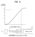
- FIG. 8 is an output voltage diagram showing a correspondence between the output of the system of measuring the perpendicular position of the polishing pad surface in the CMP machine used in the semiconductor integrated circuit device manufacturing method of the embodiment of the invention and the positional relationship between a sensor body and a displacement body of a sensor in the CMP machine.
- FIG. 9 is a schematic side sectional view showing a processing flow of polishing operation of the CMP machine used in the semiconductor integrated circuit device manufacturing method of the embodiment of the invention.
- FIG. 10 is a time chart showing a processing sequence in first and second platens in the CMP machine used in the semiconductor integrated circuit device manufacturing method of the embodiment of the invention.
- FIG. 11 is a sectional view of a device at an initial stage in a CMP process in the semiconductor integrated circuit device manufacturing method of the embodiment of the invention.
- FIG. 12 is a sectional view of the device at a middle stage in the CMP process in the semiconductor integrated circuit device manufacturing method of the embodiment of the invention.
- FIG. 13 is a sectional view of the device at a final stage in the CMP process in the semiconductor integrated circuit device manufacturing method of the embodiment of the invention.
- FIG. 14 is a schematic sectional structural view illustrating an ordinary sectional structure of a device obtained by the semiconductor integrated circuit device manufacturing method of the embodiment of the invention.
- step (b) comprises the substeps of: (i) pressing a rotating dresser to a polishing pad, thereby carrying out dressing treatment; (ii) supplying a polishing slurry to the polishing pad while moving the pad and the wafer relatively in a state that the first main surface of the wafer is pressed to the polishing pad; and (iii) measuring the position of the dresser in the direction perpendicular to the surface of the polishing pad in the substep (i), thereby detecting the abrasion amount and the thickness of the polishing pad indirectly.
- a first platen 4 a will be mainly described. The description can be basically applied, as it is, to any other platen; thus, about the same or similar members or portions in the platens, repeated description will not be made.
- FIG. 1 illustrates a situation that CMP treatment of a wafer la and dressing treatment of a polishing pad 2 are simultaneously conducted (in the embodiment, a wafer having a diameter of 300 mm is used as an example of the wafer 1 a ).
- the polishing pad is rotated by an autorotating/revolving mechanism 12 .
- a polishing slurry 14 is supplied from a slurry supplying section 15 .
- a rotatable dresser 3 a is held by a dresser holding rotary section 5 which can be stretched and shrunken up and down.
- This dresser holding rotary section 5 is coupled to a dresser head section 6 so as to be rotatable.
- This dresser head section 6 is fixed to a supporting pole 8 , which can be rotated on its axis, through an arm 7 a .
- This supporting pole 8 is rotatably fixed to the base stand 9 .
- To this dresser head section 6 is fitted a displacement sensor body having a sensor head 21 and a detecting coil 22 .
- the sensor body is combined with a displacement body (metallic pipe) 23 (see FIG. 3 ) fitted to the dresser side of the dresser holding rotary section 5 to form a displacement sensor.
- FIG. 2 is a top view illustrating the situation that the CMP treatment of the wafer 1 a and the dressing treatment of the polishing pad 2 are simultaneously conducted.
- the dresser 3 a is rotated on its axis and further the dresser 3 a is repeatedly swung as shown by a broken line.
- the dresser 3 a passes over almost all of points at which the wafer actually contacts on the polishing pad 2 .
- the rotational speed of each of the platens is, for exampie, 63rpm, the rotational speed of the dresser (the dresser diameter: for example, about 10 cm) is 90 rpm, the dressing load is 7 lbf (about 3 kgw), the swing speed, which is also called the sweep frequency, is 19 times/minute (one reciprocation corresponds to one time), and the swing width of the center of the dresser is 43 cm.
- the diameter of the wafer 1 a is smaller than that of the dresser 3 a in this manner; thus, in this case, the controllability of the dressing becomes better than in the case of using a dresser having a larger diameter.
- the dresser that be used is, for example, a dresser as used in this embodiment, wherein dressing particles, such as diamond grains, are embedded in a substantially entire surface of a disc, a dresser wherein the same processing is applied to a substrate in a ring form, or a dresser wherein plural dresser plates in the form of segments are fixed, into a ring form, to the circumference of a disc.
- the diameter of the dresser referred to in the present application is substantially equal to the diameter of the disc, the substrate, or any other base plate or substrate.
- FIG. 3 is an enlarged view illustrating the dresser head section 6 of the dresser mechanism, and a portion of the mechanism positioned ahead of the head section 6 .
- the dresser mechanism is described as follows. To the center of the dresser head section 6 is fixed the sensor head 21 , and the coil 22 is projected from the lower plane of this sensor head 21 . About the displacement body 23 , its lower end is fixed to a lower structure 5 b of the dresser holding rotary section 5 , and a part of the coil 22 is inserted into the displacement body 23 .
- This lower structure 5 b of the dresser holding rotary section 5 is coupled to an upper structure 5 a through an up-and-down sliding section 25 in such a manner that the lower structure 5 b can be slid up and down and can transmit rotation.
- the upper structure 5 a is rotatably coupled to the dresser head 6 through a bearing 24 .
- the dresser (dressing plate or conditioner plate) 3 a is coupled to the lower end of the lower structure 5 b through a flexible connector 26 which can transmit rotation and freely swings up and down.
- the lower end of the lower structure 5 b and the dresser 3 a follow the pad surface by action of a compliance mechanism 27 .
- a displacement sensor may be fitted to the supporting pole 8 to measure the displacement of the upper portion of the supporting pole and that of the lower portion thereof with respect to the fitted sensor position.
- FIG. 4 is a schematic sectional view of the dresser 3 a .
- the dresser 3 a is generally formed by fixing diamond grains 17 , which may be placed into other dressing grains, onto a metallic disc 18 made of nickel, titanium or the like by electroplating.
- FIG. 5 is a top view of the whole of the CMP machine.
- This machine has a second platen 4 b and a third platen 4 c besides the first platen 4 a , and the wafer 1 inside a hoop (semiconductor wafer sealing container) 82 on a load port 81 is received in an input station 32 by a handling robot 31 in a state that a first main surface of the wafer 1 is faced downwards, and the wafer 1 is placed in position by means of a load cup 34 and is adsorbed onto each of polishing heads 11 a , 11 b , 11 c and 11 d .
- hoop semiconductor wafer sealing container
- the wafer 1 In a state that the wafer 1 is held by the polishing head, the wafer 1 is successively rotated around the three platens 4 a , 4 b and 4 c by means of the autorotating/revolving mechanism 12 , so as to be subjected to polishing treatment. Finally, the wafer 1 is shifted to an output station 33 via the load cup 34 . Therefrom, the wafer 1 is returned to the hoop 82 by the handling robot 31 .
- the platens are equipped with dresser mechanisms (or polishing pad conditioning mechanism), respectively. The mechanisms are made of dressers 3 a , 3 b and 3 c , arms 7 a , 7 b and 7 c , and others, respectively.
- FIG. 6 is a structural view of a perpendicular position measuring circuit 41 , and a controlling/driving system of the CMP machine based on signals from the circuit 41 .
- the sensor head section 21 reads out a change in positional relationship between the displacement body 23 , which may be made of a brass pipe, and the sensor rod section (coil) 22 , and then a signal corresponding to the read value is sent to an amplifier 42 , so as to be subjected to amplifying treatment and other treatments.
- an amplifier 42 to these elements is supplied electric power from a power supply circuit 43 .
- the measured result is then outputted to the CMP machine control system 44 .
- the CMP machine control system 44 controls a polishing driving system 45 and a dresser driving system 85 (control action: for example, real-time control of the dressing time and the dressing pressure). Moreover, on the basis of the signal, the CMP machine control system 44 controls an alarm display system 86 to display an alarm (display action: for example, display of the coming of the time when the polishing pad should be exchanged). Furthermore, the system 44 stores various data or sends out the same to the outside (for example, a host control system of a factory or an external data processing system 91 ) through a communication channel (data log storing action, and other data storing/sending actions: for example, sending of dressing rate data to an external control system).
- FIG. 7 is a circuit action explanatory view, with reference to which the action of the perpendicular position measuring circuit 41 will be described.
- a pulse signal is applied thereto, the waveform B of the voltage, in a condenser C, supplied through a resistance R is smoothed by the inductance of the coil 22 .
- the gradient of the waveform is varied by an effect of eddy current.
- a sensor output is obtained (specifically, the voltage waveform B is detected, thereby giving the output).
- the dotted line represents the waveform when the pipe 23 is inserted, and the solid line represents the waveform when the pipe 23 is pulled out.
- the period of the pulse signal is set to carry out sampling at 10 times per second.
- FIG. 8 is an action-explaining chart illustrating the output of the perpendicular position measuring circuit 41 and the positional relationship between the displacement body 23 and the coil 22 . It is understood from this chart that as the length by which the coil 22 is covered with the pipe 23 becomes larger, the output becomes smaller.
- FIG. 9 is a schematic side sectional view, referring to which a description will be made about the movement of wafers 1 a , 1 b and 1 c to be treated between the platens 4 a , 4 b and 4 c shown in FIG. 5 , which has illustrated the whole of the CMP machine.
- the wafer la is positioned on the first platen 4 a , and is subjected to primary polishing (at this time, the wafer 1 b is positioned on the second platen, and the wafer 1 c is positioned on the third platen).
- the wafer 1 a is shifted to the second platen, and subjected to secondary polishing (at this time, the wafer 1 b is positioned on the third platen, and the CMP treatment of the wafer 1 c is already finished; a new wafer is supplied to the first platen 4 a ; thereafter, a similar matter will be repeated).
- the wafer 1 a is then shifted to the third platen, and subjected to the so-called water-polishing (tertiary polishing). That is, the wafer 1 a is subjected to finish polishing by means of the polishing pads without using any slurry while only pure water or liquid chemical is supplied thereto.
- FIG. 10 is a time chart showing a situation of the wafer polishing treatment and the dressing treatment on each of the polishing pads in FIG. 9 .
- dressing is first started at a time t 1 to adjust the state of the pad.
- polishing of the wafer is started at a time t 2 (“dressing precedent time”, that is, the period from t 1 to t 2 is, for example, about 12 seconds).
- dressing is early ended at a time t 3 (“dressing/polishing parallel processing time”, that is, the period from t 2 to t 3 is, for example, about 60seconds).
- polishing independent processing time that is, the period from t 3 to t 4 is, for example, about 3 seconds.
- non-processing timel that is, the period from t 4 to t 5 is, for example, about 15 seconds. The cycle is then repeated.
- non-processing timel that is, the period from t 4 to t 5 is, for example, about 15 seconds.
- the polishing pad thickness is measured in 120 points of the polishing pad (the number of sweeps: about 4, the number of platen rotations: about 12, and the number of dresser rotations: about 8) in the dressing precedent time.
- the dressing precedent time is shortened or extended in real time on the basis of the measurement data (conversely, “polishing time” t 2 ⁇ t 4 may be shortened or extended) however, the former is advantageous from the viewpoint of the life span of the dresser), so as to make it possible to maintain an appropriate polishing amount and an appropriate polishing property all times.
- an appropriate pad state may be maintained by controlling the dressing pressure at each of the points without varying the dressing precedent time or the polishing time (this manner is advantageous from the viewpoint of throughput).
- an appropriate polishing state may be maintained.
- processing as described below is provided. First, on the basis of the polishing pad data obtained in the dressing/polishing parallel processing time, a subsequent wafer processing (polishing treatment or dressing treatment) is subjected to feed back correction/control. Second, on the basis of the polishing pad data obtained in the dressing precedent time, polishing treatment of the wafer to be treated in the present step is corrected/controlled in real time.
- the dressing treatment is corrected/controlled in real time.
- subsequent treatment will be corrected through communication with a host system.
- FIGS. 11 to 13 are sectiona 1 views of the device, which correspond to the treatment steps shown in FIG. 10 .
- FIG. 11 shows a step before the primary polishing. Specifically, FIG. 11 shows a situation that in the first main surface 16 of the wafer 1 , a silicon oxide film 52 formed by CVD (chemical vapor deposition) using HDP (high density plasma) is embedded in STI (shallow trench isolation) trenches or the like made in the surface of the substrate (wafer 1 a ). On the surface of the substrate 1 a , a patterned silicon nitride film 51 , which is used as a CMP stopper or the like, is formed.
- CVD chemical vapor deposition
- HDP high density plasma
- FIG. 12 is a sectional view illustrating a state of the device when the primary polishing is finished
- FIG. 13 is a sectional view illustrating a state of the device when the secondary polishing is finished.
- FIG. 14 illustrates a sectional structure of the device when the process is finished.
- This device has a wiring structure made of four ordinary aluminum-wiring layers as lower layers, three copper damascene wiring layers as upper layers, and aluminum bonding pads as the topmost layer.
- n type wells 61 and p type wells 62 are present, and in each of the wells, a p-type source or drain region 63 and an n type source or drain region 64 are formed.
- gate electrodes 65 of P-type MOS-FETs and gate electrodes 66 of N type MOS-FETs are positioned, and tungsten plugs 67 are embedded in contact holes in a lowermost interlayer dielectric 69 .
- Aluminum wires 68 (wires containing aluminum as a principal component), the upper and lower surfaces of which are sandwiched between barrier metals, are made on the lowermost interlayer dielectric 69 .
- Embedded copper wires 70 are formed in the 5 th wiring layer and all the wiring layers thereon.
- a cap insulation layer 71 is formed, , and bonding pads 74 are made in opening in the layer 71 .
- two-layer structure comprised of a lower plasma silicon nitride film 72 and an upper polyimide film 73 forms a final passivation film.
- CMP treatment is applied mainly to: insulated film CMP processes, such as flattening in the step of the above-mentioned STI, and in the formation of the interlayer dielectrics (the interlayer dielectrics and the in-layer dielectrics in the illustrated embodiment) of the (1 st to 4 th ) aluminum wiring layers using HDP or the like; and metal CMP processes, that is, the following removal after the copper wiring is formed by plating with copper or some other method in the dual damascene wiring moieties (the 5 th to 7 th wiring layers): removal of unnecessary portions of the metal.
- the same metal CMP process is applied also to the contact plugs 67 or tungsten plugs on the aluminum wiring layer.
- the present invention may be applied to the two cases.
- the invention is applied in particular to a CMP process for a silicon oxide film system or a silicon system, wherein polishing pads are intensely worn away, large advantageous effects can be expected.
- measurement is made without using light; therefore, the invention has an advantage that corrosion based on photoelectric effect or the like is not caused in metal CMP of copper damascene wiring.
- the state of any one of the polishing pads can be measured through the dresser which contacts the pad directly; therefore, the time for the exchange of the pad, the state of the dresser, or the like can be precisely determined in real time.
- the type of the dresser and the dressing rate based on the dressing pressure can be measured and stored in real time; therefore, the dressing period can easily be made appropriate.
- the relationship between the abrasion amount of the polishing pads and the dressing time or the like can be determined continuously; therefore, the generation of a treatment abnormality can be found at an early stage from the data.
- a desired measurement can be made in real time with a relatively simple sensor; therefore, the machine for the invention can be made having an inexpensive structure.
- the invention can be applied to, for example, a CMP process using a single disc-form polishing pad, or a CMP process using a belt-form polishing pad.
Landscapes
- Engineering & Computer Science (AREA)
- Mechanical Engineering (AREA)
- Computer Hardware Design (AREA)
- Condensed Matter Physics & Semiconductors (AREA)
- General Physics & Mathematics (AREA)
- Manufacturing & Machinery (AREA)
- Physics & Mathematics (AREA)
- Microelectronics & Electronic Packaging (AREA)
- Power Engineering (AREA)
- Mechanical Treatment Of Semiconductor (AREA)
- Finish Polishing, Edge Sharpening, And Grinding By Specific Grinding Devices (AREA)
- Grinding-Machine Dressing And Accessory Apparatuses (AREA)
- Constituent Portions Of Griding Lathes, Driving, Sensing And Control (AREA)
Abstract
Description
- 1. A manufacturing method of a semiconductor integrated circuit device, comprising the steps of: (a) forming a first member layer over a first main surface of a wafer; and (b) applying chemical mechanical polishing to the first member layer in a chemical mechanical polishing machine, wherein the step (b) comprises the substeps of: (i) pressing a rotating dresser to a polishing pad, thereby carrying out dressing treatment; (ii) supplying a polishing slurry to the polishing pad while moving the pad and the wafer relatively in a state that the first main surface of the wafer is pressed to the polishing pad; and (iii) measuring the position of the dresser in the direction perpendicular to the surface of the polishing pad in the substep (i), thereby detecting the abrasion amount and the thickness of the polishing pad indirectly.
- 2. The manufacturing method of a semiconductor integrated circuit device according to
item 1, wherein at least one portion of a first term when the substep (i) is performed and at least one portion of a second term when the substep (ii) is performed overlap with each other. - 3. The manufacturing method of a semiconductor integrated circuit device according to
item 1 oritem 2, wherein the first member layer is an insulation layer. - 4. The manufacturing method of a semiconductor integrated circuit device according to any one of
item 1 toitem 3, wherein the first member layer comprises a silicon oxide film as a principal constituent film. - 5. The manufacturing method of a semiconductor integrated circuit device according to any one of
item 1 toitem 4, wherein about the first term when the substep (i) is performed and the second term when the substep (ii) is performed, main portions thereof overlap with each other. - 6. The manufacturing method of a semiconductor integrated circuit device according to any one of
item 1 toitem 5, wherein the perpendicular position is measured without bringing a sensor into direct contact with the polishing pad. - 7. The manufacturing method of a semiconductor integrated circuit device according to any one of
item 1 toitem 6, wherein the perpendicular position is measured without using light. - 8. The manufacturing method of a semiconductor integrated circuit device according to any one of
item 1 to item 7, wherein the polishing pad is rotating in the substeps (i) and (ii). - 9. The manufacturing method of a semiconductor integrated circuit device according to
item 8, wherein the wafer is rotating in the substep (ii). - 10. The manufacturing method of a semiconductor integrated circuit device according to any one of
item 1 toitem 9, wherein about the dresser, the position thereof in the direction of the radius of the polishing pad is varied over the polishing pad in the substep (i). - 11. The manufacturing method of a semiconductor integrated circuit device according to any one of
item 1 to item 10, wherein the perpendicular position is measured plural times in the first term when the substep (i) is performed. - 12. The manufacturing method of a semiconductor integrated circuit device according to any one of
item 1 to item 11, wherein the dresser is fixed to a dresser holding rotary section, the dresser holding rotary section can be controlled to be stretched and shrunken up and down, the rotary section itself is rotatably held by a dresser head section, the dresser head section is held by a dresser supporting section through a dresser arm, and the dresser supporting section is held by a base of the chemical mechanical polishing machine so as to be optionally rotated on its axis of the section. - 13. The manufacturing method of a semiconductor integrated circuit device according to any one of
item 1 toitem 12, wherein the perpendicular position is measured through a displacement sensor comprising a sensor body comprising a coil section, and a displacement body. - 14. The manufacturing method of a semiconductor integrated circuit device according to item 13, wherein the sensor body is fitted to the dresser head section, which holds the dresser.
- 15. The manufacturing method of a semiconductor integrated circuit device according to item 13 or
item 14, wherein the displacement body is fixed to the dresser holding rotary section. - 16. The manufacturing method of a semiconductor integrated circuit device according to any one of item 13 to
item 15, wherein the displacement sensor is a sensor for measuring, electrically, a change in the impedance of the coil section in the displacement sensor on the basis of a displacement of an object to be measured. - 17. The manufacturing method of a semiconductor integrated circuit device according to any one of
item 1 to item 11, wherein the dresser is fixed to a dresser holding rotary section, the dresser holding rotary section is rotatably held by a dresser head section, the dresser head section is held by a dresser supporting section through a dresser arm, and the dresser supporting section is held by a base of the chemical mechanical polishing machine so as to be optionally moved up and down and rotated on its axis of the section. - 18. The manufacturing method of a semiconductor integrated circuit device according to
item 17, wherein the perpendicular position is measured through a displacement sensor comprising a sensor body comprising a coil section, and a displacement body. - 19. The manufacturing method of a semiconductor integrated circuit device according to
item 18, wherein the displacement sensor is fitted to the dresser supporting section. - 20. The manufacturing method of a semiconductor integrated circuit device according to
item 18 or item 19, wherein the perpendicular position is measured by measuring the up-and-down motion of the dresser supporting section through the displacement sensor.
- 21. A manufacturing method of a semiconductor integrated circuit device, comprising the steps of: (a) forming a first member layer over a first main surface of a wafer; and (b) applying chemical mechanical polishing to the first member layer in a chemical mechanical polishing machine,
- 1. In the present application, for the sake of convenience, any embodiment may be divided into plural sections as the case may be, so as to be described in accordance with the sections. However, these are not independently of each other; thus, these may be individual sections of a single example, or one thereof may be details of a part of the other(s) or may be a modification of a part or the whole of the other(s) except any case where it is evidently stated that such a matter is not applicable to the case. In principle, about the same members or portions, repeated description is omitted. Each of constituting elements in any embodiment is not essential except any case where it is evidently stated that this matter is not applicable to the case, any case to this matter is theoretically not applicable, and any case to which this matter is clearly interpreted not to be applicable from the context.
- 2. In connection with any material, any composition or the like in the description of embodiments and others, in the case of using the wording “X made of A” or the like, a matter that an element other than A is contained as a principal constituting element is excluded except any case where it is evidently stated that this matter is not applicable to the case, any case to this matter is theoretically not applicable, and any case to which this matter is clearly interpreted not to be applicable from the context in the same manner as described above. For example, the wording “X made of A” means that “X contains A as a principal component”. It is heedless to say that, for example, the wording “silicon member” is not limited to a member comprised of pure silicon, and includes, in the category thereof, a member containing SiGe alloy or some other multi-component alloy containing silicon as a principal component, and a member containing not only Si but also other additives. In the same manner, it is needless to say that the wording “silicon oxide film” include, in the category thereof, an undoped silicon dioxide film, which is relatively pure, a FSG (fluorosilicate glass) film, a TEOS-based silicone oxide film, a SiOC (silicon oxycarbide) film, a carbon-doped silicon oxide film, thermal oxide films such as ODG (organosilicate glass), PSG (phosphorous silicate glass) and BPSG (borophosphosilicate glass) films, a CVD oxide film, painted silicon oxide films such as SOG (spin on glass) and NSC (nano-clustering silica) films, a silica-based low-k insulated film (porous insulated film), wherein pores are incorporated into any one of the same films as described above, and a composite film containing any one of the above-mentioned films, as a principal element, which is combined with a different silicon-based insulated film (silica-based insulated film).
- 3. In the same manner, about some figures, positions, attributes, and others, preferred examples will be described. However, it is needless to say that the figures and so on are not strictly limited to the preferred examples except any case where it is evidently stated that this matter is not applicable to the case, and any case to which this matter is clearly interpreted not to be applicable from the context.
- 4. When a specific numerical value or quantity is referred to, numerical values or quantities over or below the numerical value or quantity are allowable except any case where it is evidently stated that this matter is not applicable to the case, any case to this matter is theoretically not applicable, and any case to which this matter is clearly interpreted not to be applicable from the context.
- 5. The wording “wafer” usually denotes a monocrystal silicon wafer, on which a semiconductor integrated circuit device, which may be called a semiconductor device or an electron device, is to be formed. However, it is needless to say that the wording includes, in the category thereof, an epitaxial wafer, and a composite wafer containing an insulated substrate plus a semiconductor layer or the like.
Claims (18)
Applications Claiming Priority (2)
| Application Number | Priority Date | Filing Date | Title |
|---|---|---|---|
| JP2007149901A JP2008305875A (en) | 2007-06-06 | 2007-06-06 | Method of manufacturing semiconductor integrated circuit device |
| JP2007-149901 | 2007-06-06 |
Publications (2)
| Publication Number | Publication Date |
|---|---|
| US20080305715A1 US20080305715A1 (en) | 2008-12-11 |
| US7722437B2 true US7722437B2 (en) | 2010-05-25 |
Family
ID=40096313
Family Applications (1)
| Application Number | Title | Priority Date | Filing Date |
|---|---|---|---|
| US12/116,958 Expired - Fee Related US7722437B2 (en) | 2007-06-06 | 2008-05-08 | Manufacturing method of semiconductor integrated circuit device |
Country Status (5)
| Country | Link |
|---|---|
| US (1) | US7722437B2 (en) |
| JP (1) | JP2008305875A (en) |
| KR (1) | KR20080107285A (en) |
| CN (1) | CN101320708A (en) |
| TW (1) | TW200915408A (en) |
Cited By (3)
| Publication number | Priority date | Publication date | Assignee | Title |
|---|---|---|---|---|
| US20120270477A1 (en) * | 2011-04-22 | 2012-10-25 | Nangoy Roy C | Measurement of pad thickness and control of conditioning |
| US20120270474A1 (en) * | 2011-04-20 | 2012-10-25 | Nanya Technology Corporation | Polishing pad wear detecting apparatus |
| US11685013B2 (en) | 2018-01-24 | 2023-06-27 | Taiwan Semiconductor Manufacturing Company, Ltd. | Polishing pad for chemical mechanical planarization |
Families Citing this family (19)
| Publication number | Priority date | Publication date | Assignee | Title |
|---|---|---|---|---|
| EP2306506B1 (en) * | 2009-10-01 | 2013-07-31 | ams AG | Method of producing a semiconductor device having a through-wafer interconnect |
| CN102398212A (en) * | 2010-09-17 | 2012-04-04 | 中芯国际集成电路制造(上海)有限公司 | Chemical mechanical polishing equipment |
| US20130017762A1 (en) * | 2011-07-15 | 2013-01-17 | Infineon Technologies Ag | Method and Apparatus for Determining a Measure of a Thickness of a Polishing Pad of a Polishing Machine |
| CN103084969B (en) * | 2011-11-01 | 2015-09-09 | 中芯国际集成电路制造(上海)有限公司 | A kind of chemical-mechanical grinding device |
| CN102423870B (en) * | 2011-11-28 | 2014-03-26 | 浙江工业大学 | Trace grinding thickness measuring device |
| CN103522188B (en) * | 2012-07-02 | 2018-07-20 | 中芯国际集成电路制造(上海)有限公司 | Grinding pad method for sorting, grinder pad finisher and grinder station |
| KR101630423B1 (en) * | 2014-12-22 | 2016-06-24 | 주식회사 포스코 | Dressing scattering covering device and specimen grinder provided with the saem |
| JP6465345B2 (en) * | 2014-12-26 | 2019-02-06 | 株式会社荏原製作所 | Method and apparatus for measuring surface properties of polishing pad |
| TWI821887B (en) * | 2016-11-29 | 2023-11-11 | 日商東京威力科創股份有限公司 | Substrate treatment device, substrate treatment method and recording medium |
| CN107553330B (en) * | 2017-10-20 | 2019-07-12 | 德淮半导体有限公司 | Finishing disc system, chemical mechanical polishing device and conditioner discs fall off method for detecting |
| CN108109990B (en) * | 2017-12-15 | 2020-12-18 | 浙江清华柔性电子技术研究院 | Through silicon via adapter plate for system-in-package |
| CN108044508A (en) * | 2018-01-02 | 2018-05-18 | 北京半导体专用设备研究所(中国电子科技集团公司第四十五研究所) | A kind of detection device and method |
| CN108687648A (en) * | 2018-05-22 | 2018-10-23 | 武汉新芯集成电路制造有限公司 | A kind of monitoring device and monitoring method of grinding pad |
| CN111421462B (en) * | 2019-01-08 | 2022-03-22 | 中芯国际集成电路制造(上海)有限公司 | Chemical mechanical polishing method |
| CN109500741B (en) * | 2019-01-11 | 2020-07-07 | 北京半导体专用设备研究所(中国电子科技集团公司第四十五研究所) | Trimming device and polishing equipment with measure polishing pad thickness |
| CN111515863A (en) * | 2020-04-30 | 2020-08-11 | 武汉新芯集成电路制造有限公司 | Polishing method and polishing pad dressing system |
| CN111409015B (en) * | 2020-05-08 | 2020-11-13 | 苏州航菱微精密组件有限公司 | Grinding machine mechanism, grinding process and preparation process of grinding material of grinding machine mechanism |
| CN113458972A (en) * | 2021-07-28 | 2021-10-01 | 北京烁科精微电子装备有限公司 | Polishing pad dressing device and polishing equipment |
| CN114633206A (en) * | 2022-04-25 | 2022-06-17 | 北京烁科精微电子装备有限公司 | Trimming device and wafer polishing system |
Citations (12)
| Publication number | Priority date | Publication date | Assignee | Title |
|---|---|---|---|---|
| JPH09290363A (en) | 1996-04-26 | 1997-11-11 | Sumitomo Metal Ind Ltd | Polishing method and polishing device |
| JPH1086056A (en) | 1996-09-11 | 1998-04-07 | Speedfam Co Ltd | Management method and device for polishing pad |
| JPH11207572A (en) | 1997-11-05 | 1999-08-03 | Aplex Inc | Polishing device incorporating wear monitoring means for polishing pad, and control method for the same |
| JP2000271854A (en) | 1999-03-25 | 2000-10-03 | Hitachi Ltd | Machining method and device thereof, and machining method for semiconductor substrate |
| JP2001079752A (en) | 1999-09-08 | 2001-03-27 | Hitachi Ltd | Chemical machine polishing device and method for manufacturing semiconductor integrated circuit device using it |
| US6322434B1 (en) * | 1999-03-11 | 2001-11-27 | Ebara Corporation | Polishing apparatus including attitude controller for dressing apparatus |
| US20020160609A1 (en) * | 2001-04-25 | 2002-10-31 | Souichi Katagiri | Method and apparatus for manufacturing semiconductor device |
| US6609962B1 (en) * | 1999-05-17 | 2003-08-26 | Ebara Corporation | Dressing apparatus and polishing apparatus |
| US6835116B2 (en) * | 2000-01-21 | 2004-12-28 | Ebara Corporation | Polishing apparatus |
| US7070479B2 (en) * | 2001-06-22 | 2006-07-04 | Infineon Technologies Ag | Arrangement and method for conditioning a polishing pad |
| US20080070479A1 (en) * | 2004-11-01 | 2008-03-20 | Ebara Corporation | Polishing Apparatus |
| US20080090499A1 (en) * | 2005-08-30 | 2008-04-17 | Tokyo Seimitsu Co., Ltd. | Pad conditioner, pad conditioning method, and polishing apparatus |
-
2007
- 2007-06-06 JP JP2007149901A patent/JP2008305875A/en not_active Withdrawn
-
2008
- 2008-05-08 US US12/116,958 patent/US7722437B2/en not_active Expired - Fee Related
- 2008-05-20 TW TW097118540A patent/TW200915408A/en unknown
- 2008-06-03 CN CNA2008100859166A patent/CN101320708A/en active Pending
- 2008-06-04 KR KR1020080052562A patent/KR20080107285A/en not_active Application Discontinuation
Patent Citations (14)
| Publication number | Priority date | Publication date | Assignee | Title |
|---|---|---|---|---|
| JPH09290363A (en) | 1996-04-26 | 1997-11-11 | Sumitomo Metal Ind Ltd | Polishing method and polishing device |
| JPH1086056A (en) | 1996-09-11 | 1998-04-07 | Speedfam Co Ltd | Management method and device for polishing pad |
| US6040244A (en) | 1996-09-11 | 2000-03-21 | Speedfam Co., Ltd. | Polishing pad control method and apparatus |
| JPH11207572A (en) | 1997-11-05 | 1999-08-03 | Aplex Inc | Polishing device incorporating wear monitoring means for polishing pad, and control method for the same |
| US5934974A (en) | 1997-11-05 | 1999-08-10 | Aplex Group | In-situ monitoring of polishing pad wear |
| US6322434B1 (en) * | 1999-03-11 | 2001-11-27 | Ebara Corporation | Polishing apparatus including attitude controller for dressing apparatus |
| JP2000271854A (en) | 1999-03-25 | 2000-10-03 | Hitachi Ltd | Machining method and device thereof, and machining method for semiconductor substrate |
| US6609962B1 (en) * | 1999-05-17 | 2003-08-26 | Ebara Corporation | Dressing apparatus and polishing apparatus |
| JP2001079752A (en) | 1999-09-08 | 2001-03-27 | Hitachi Ltd | Chemical machine polishing device and method for manufacturing semiconductor integrated circuit device using it |
| US6835116B2 (en) * | 2000-01-21 | 2004-12-28 | Ebara Corporation | Polishing apparatus |
| US20020160609A1 (en) * | 2001-04-25 | 2002-10-31 | Souichi Katagiri | Method and apparatus for manufacturing semiconductor device |
| US7070479B2 (en) * | 2001-06-22 | 2006-07-04 | Infineon Technologies Ag | Arrangement and method for conditioning a polishing pad |
| US20080070479A1 (en) * | 2004-11-01 | 2008-03-20 | Ebara Corporation | Polishing Apparatus |
| US20080090499A1 (en) * | 2005-08-30 | 2008-04-17 | Tokyo Seimitsu Co., Ltd. | Pad conditioner, pad conditioning method, and polishing apparatus |
Cited By (3)
| Publication number | Priority date | Publication date | Assignee | Title |
|---|---|---|---|---|
| US20120270474A1 (en) * | 2011-04-20 | 2012-10-25 | Nanya Technology Corporation | Polishing pad wear detecting apparatus |
| US20120270477A1 (en) * | 2011-04-22 | 2012-10-25 | Nangoy Roy C | Measurement of pad thickness and control of conditioning |
| US11685013B2 (en) | 2018-01-24 | 2023-06-27 | Taiwan Semiconductor Manufacturing Company, Ltd. | Polishing pad for chemical mechanical planarization |
Also Published As
| Publication number | Publication date |
|---|---|
| KR20080107285A (en) | 2008-12-10 |
| TW200915408A (en) | 2009-04-01 |
| JP2008305875A (en) | 2008-12-18 |
| CN101320708A (en) | 2008-12-10 |
| US20080305715A1 (en) | 2008-12-11 |
Similar Documents
| Publication | Publication Date | Title |
|---|---|---|
| US7722437B2 (en) | Manufacturing method of semiconductor integrated circuit device | |
| US11358252B2 (en) | Method of using a polishing system | |
| US20070238395A1 (en) | Substrate polishing apparatus and substrate polishing method | |
| KR20010042086A (en) | Apparatus and method for film thickness measurement integrated into a wafer load/unload unit | |
| US20090209176A1 (en) | Method and apparatus for polishing object | |
| JP3321338B2 (en) | Semiconductor device manufacturing method and manufacturing apparatus | |
| JP2013036881A (en) | Polishing monitoring method and polishing device | |
| US6875086B2 (en) | Surface planarization | |
| US6609950B2 (en) | Method for polishing a substrate | |
| US7166015B2 (en) | Apparatus and method for controlling fluid material composition on a polishing pad | |
| US6136138A (en) | Method and apparatus for chemical mechanical polishing of a semiconductor wafer | |
| JPH08139060A (en) | Method of manufacturing semiconductor device and chemical machine polisher | |
| JP2001079752A (en) | Chemical machine polishing device and method for manufacturing semiconductor integrated circuit device using it | |
| JP6510348B2 (en) | Substrate processing apparatus, substrate processing system, and substrate processing method | |
| JPH10256209A (en) | Polishing equipment | |
| EP1340248A2 (en) | Method for determining an endpoint and semiconductor wafer | |
| KR100583210B1 (en) | Chemical Mechanical Polishing Apparatus and Method | |
| US20200055160A1 (en) | Chemical mechanical polishing method and apparatus | |
| JP2002025959A (en) | Grinding apparatus of semiconductor substrate | |
| JP7330254B2 (en) | Correction of slurry composition in in-situ electromagnetic induction monitoring | |
| JP2005169593A (en) | Polishing device, polishing method, manufacturing method of semiconductor device using the method, and semiconductor device manufactured by the method | |
| US20040214508A1 (en) | Apparatus and method for controlling film thickness in a chemical mechanical planarization system | |
| JPH09306879A (en) | Method of chemically/mechanically making work planar | |
| KR100778859B1 (en) | Apparatus for chemical mechanical polishing | |
| JPH081503A (en) | Polishing device for wafer |
Legal Events
| Date | Code | Title | Description |
|---|---|---|---|
| AS | Assignment |
Owner name: RENESAS TECHNOLOGY CORP., JAPAN Free format text: ASSIGNMENT OF ASSIGNORS INTEREST;ASSIGNOR:ITO, YOSHINORI;REEL/FRAME:020918/0297 Effective date: 20080317 Owner name: RENESAS TECHNOLOGY CORP.,JAPAN Free format text: ASSIGNMENT OF ASSIGNORS INTEREST;ASSIGNOR:ITO, YOSHINORI;REEL/FRAME:020918/0297 Effective date: 20080317 |
|
| AS | Assignment |
Owner name: NEC ELECTRONICS CORPORATION, JAPAN Free format text: MERGER;ASSIGNOR:RENESAS TECHNOLOGY CORP.;REEL/FRAME:024879/0190 Effective date: 20100401 Owner name: RENESAS ELECTRONICS CORPORATION, JAPAN Free format text: CHANGE OF NAME;ASSIGNOR:NEC ELECTRONICS CORPORATION;REEL/FRAME:024864/0635 Effective date: 20100401 |
|
| FEPP | Fee payment procedure |
Free format text: PAYOR NUMBER ASSIGNED (ORIGINAL EVENT CODE: ASPN); ENTITY STATUS OF PATENT OWNER: LARGE ENTITY |
|
| REMI | Maintenance fee reminder mailed | ||
| LAPS | Lapse for failure to pay maintenance fees | ||
| STCH | Information on status: patent discontinuation |
Free format text: PATENT EXPIRED DUE TO NONPAYMENT OF MAINTENANCE FEES UNDER 37 CFR 1.362 |
|
| FP | Lapsed due to failure to pay maintenance fee |
Effective date: 20140525 |