BACKGROUND OF THE INVENTION
1. Field of the Invention
The present invention relates to a surface acoustic wave device including a piezoelectric substrate, an IDT electrode, and a SiO2 film covering the piezoelectric substrate and the IDT electrode. In particular, the present invention relates to a surface acoustic wave device including an IDT electrode formed by filling grooves provided in the upper surface of a piezoelectric substrate with a metal.
2. Description of the Related Art
Duplexers (DPX) and RF filters, which are used for mobile communication systems such as mobile phones, are required to have broadband characteristics and good temperature characteristics. Surface acoustic wave devices have been commonly used as DPXs and RF filters.
Surface acoustic wave devices used in such applications typically include a piezoelectric substrate made of LiTaO3, LiNbO3, or other suitable material and an IDT electrode thereon. LiTaO3 and LiNbO3 have negative values of a temperature coefficient of resonant frequency (TCF). To improve such temperature characteristics, one technique is known in which a SiO2 film having a positive temperature coefficient of resonant frequency is arranged on a piezoelectric substrate to cover an IDT electrode.
However, this technique produces a height difference of the SiO2 film between a portion in which fingers of an IDT electrode are provided and a portion in which the fingers of the IDT electrode are not provided. The height difference causes insertion loss to increase.
To solve this problem, Japanese Unexamined Patent Application Publication No. 2004-112748 discloses a method including forming a first insulator layer, which has substantially the same film thickness as an IDT electrode, between the IDT electrode fingers, and forming a SiO2 film to cover the IDT electrode and the first insulator layer. In this method, since the SiO2 film is formed on a substantially flat base, the SiO2 film has a substantially flat surface. The IDT electrode of the surface acoustic wave device in Japanese Unexamined Patent Application Publication No. 2004-112748 is made of a metal having a higher density than Al or an alloy primarily including the metal, or a multilayer film including a metal having a higher density than Al or an alloy primarily including the metal and another metal. The IDT electrode has a density at least about 1.5 times that of the first insulator layer.
Since the electrode of the surface acoustic wave device in Japanese Unexamined Patent Application Publication No. 2004-112748 primarily includes a metal that is heavier than Al, large variations tend to occur in the velocity and the frequency of acoustic waves which depend on variations in the thickness of the electrode. In contrast, an electrode made of Al has a very low reflection coefficient and cannot exhibit characteristics sufficiently good for surface acoustic wave resonators and surface acoustic wave filters.
To overcome such a problem, WO2006/011417A1 discloses a configuration including a piezoelectric substrate made of LiTaO3 or LiNbO3 having a plurality of grooves provided in the upper surface and an IDT electrode formed by filling the grooves with a metal, such as Al. A surface acoustic wave device of WO2006/011417A1 includes an IDT electrode formed by filling grooves with metal and a SiO2 film covering the IDT electrode. WO2006/011417A12 discloses that the SiO2 film is formed on a substantially flat base, and thus, the SiO2 film has a substantially flat surface.
WO2006/011417A1 also discloses that LiTaO3 substrates with Euler angles and LiNbO3 substrates with Euler angles (0°, 85° to 120°, 0°), (0°, 125° to 141°, 0°), (0°, 145° to 164°, 0°), or (0°, 160° to 180°, 0°) are preferably used; and LiNbO3 substrates with Euler angles (0°, 90° to 110°, 0°), (0°, 125° to 136°, 0°), (0° 149° to 159°, 0°), or (0°, 165° to 175°, 0°) are more preferably used.
A configuration intended to have improved temperature characteristics of resonant frequency that is formed by disposing a SiO2 film on an IDT electrode made of Al provides a low reflection coefficient as described above and tends to have insufficient characteristics. In contrast, since the configuration in WO2006/011417A1 includes an IDT electrode formed by filling grooves provided in a piezoelectric substrate with Al, the electrode has a sufficiently high reflection coefficient. The configuration also includes a SiO2 film and thus has improved temperature characteristics of resonant frequency. The SiO2 film has a substantially flat surface, and thus, the insertion loss does not significantly increase.
However, an inventor of the present invention has discovered that, when a response of a Rayleigh wave is utilized in the surface acoustic wave device including a LiNbO3 substrate in WO2006/011417A1, a large spurious response occurs near an attenuation pole of a main response being used. Thus, the spurious response may potentially degrade the filter characteristics and the resonance characteristics.
SUMMARY OF THE INVENTION
To overcome the problems described above, preferred embodiments of the present invention provide a surface acoustic wave device that has improved temperature characteristics of resonant frequency by including a SiO2 film, that causes little or no increase in insertion loss to increase, that has an electrode with a sufficiently high reflection coefficient, and that suppresses unwanted spurious responses, thereby having improved resonance characteristics and filter characteristics.
A surface acoustic wave device according to a preferred embodiment of the present invention includes a piezoelectric substrate having a plurality of grooves provided in a upper surface of the substrate, an IDT electrode defined by metal filled in the grooves, and a SiO2 layer arranged to cover the piezoelectric substrate and the IDT electrode and having a substantially flat upper surface, wherein the device uses a response of a Rayleigh wave excited in the piezoelectric substrate, and the piezoelectric substrate is a LiNbO3 substrate having Euler angles (0°±5°, 180° to 247°, 0°±5°).
The metal is not particularly restricted. However, a preferred metal primarily includes one metal selected from the group consisting of Al, Au, Ta, and Cu. Al, Au, Ta, and Cu, for example, are commonly used to form IDT electrodes of surface acoustic wave devices. An electrode formed by filling grooves provided in a piezoelectric substrate with any one of the metals has a sufficiently high reflection coefficient.
The metal primarily including one metal selected from the group consisting of Al, Au, Ta, and Cu may preferably be one metal selected from the group consisting of Al, Au, Ta, and Cu, or an alloy primarily including the one metal. Alternatively, the metal primarily including one metal selected from the group consisting of Al, Au, Ta, and Cu may preferably be a multilayer metal film. Such a multilayer metal film, for example, includes one metal selected from the group consisting of Al, Au, Ta, and Cu or an alloy primarily including the one metal, and an alloy primarily including one metal selected from the group consisting of Ti, Ni, Cr, NiCr, Al, and AlCu disposed thereon.
In a surface acoustic wave device according to preferred embodiments of the present invention, the metal preferably primarily includes Al, and a normalized film thickness (%) of the IDT electrode normalized with a wavelength λ of a surface acoustic wave, a normalized film thickness (%) of the SiO2 film normalized with the wavelength λ of the surface acoustic wave, and θ (°) of Euler angles (φ, θ, ψ) of LiNbO3 are within ranges shown in Table 1 below:
| TABLE 1 |
| |
| |
|
θ (°) achieving |
| IDT electrode (mainly |
|
KR 2 > 0.08 |
| containing Al) |
Thickness of SiO2 film |
and KSH 2 < 0.02 |
| |
| 2% < h/λ ≦ 6% |
17.5% < h/λ ≦ 22.5% |
210~228 |
| |
22.5% < h/λ ≦ 27.5% |
201~235 |
| |
27.5% < h/λ ≦ 32.5% |
207~229 |
| |
32.5% < h/λ ≦ 37.5% |
210~225 |
| 6% < h/λ ≦ 10% |
17.5% < h/λ ≦ 22.5% |
205~231 |
| |
22.5% < h/λ ≦ 27.5% |
204~232 |
| |
27.5% < h/λ ≦ 32.5% |
202~231 |
| |
32.5% < h/λ ≦ 37.5% |
202~232 |
| 10% < h/λ ≦ 14% |
17.5% < h/λ ≦ 22.5% |
197~239 |
| |
22.5% < h/λ ≦ 27.5% |
198~238 |
| |
27.5% < h/λ ≦ 32.5% |
194~236 |
| |
32.5% < h/λ ≦ 37.5% |
197~233 |
| 14% < h/λ ≦ 18% |
17.5% < h/λ ≦ 22.5% |
187~243 |
| |
22.5% < h/λ ≦ 27.5% |
181~242 |
| |
27.5% < h/λ ≦ 32.5% |
181~247 |
| |
32.5% < h/λ ≦ 37.5% |
188~236 |
| 18% < h/λ ≦ 22% |
17.5% < h/λ ≦ 22.5% |
180~242 |
| |
22.5% < h/λ ≦ 27.5% |
182~246 |
| |
27.5% < h/λ ≦ 32.5% |
184~238 |
| |
32.5% < h/λ ≦ 37.5% |
208~212 |
| 22% < h/λ ≦ 26% |
17.5% < h/λ ≦ 22.5% |
180~243 |
| |
22.5% < h/λ ≦ 27.5% |
181~240 |
| |
27.5% < h/λ ≦ 32.5% |
191~227 |
| |
32.5% < h/λ ≦ 37.5% |
No range achieving |
| |
|
KR 2 > 0.08 |
| |
When the metal primarily includes Al, and the normalized film thickness of the IDT electrode, the normalized film thickness of the SiO2 film, and the Euler angle of LiNbO3 are within ranges shown in Table 1, unwanted spurious responses can be effectively suppressed.
More preferably, the normalized film thickness (%) of the IDT electrode, the normalized film thickness (%) of the SiO2 film, and θ (°) of Euler angles (φ, θ, ψ) of LiNbO3 are within ranges shown in Table 2 below:
| TABLE 2 |
| |
| |
|
0 (°) achieving |
| IDT electrode (mainly |
|
KR 2 > 0.08 |
| containing Al) |
Thickness of SiO2 film |
and KSH 2 < 0.01 |
| |
| 2% < h/λ ≦ 6% |
17.5% < h/λ ≦ 22.5% |
210~228 |
| |
22.5% < h/λ ≦ 27.5% |
201~231 |
| |
27.5% < h/λ ≦ 32.5% |
208~225 |
| |
32.5% < h/λ ≦ 37.5% |
210~225 |
| 6% < h/λ ≦ 10% |
17.5% < h/λ ≦ 22.5% |
205~231 |
| |
22.5% < h/λ ≦ 27.5% |
204~232 |
| |
27.5% < h/λ ≦ 32.5% |
206~226 |
| |
32.5% < h/λ ≦ 37.5% |
202~228 |
| 10% < h/λ ≦ 14% |
17.5% < h/λ ≦ 22.5% |
197~238 |
| |
22.5% < h/λ ≦ 27.5% |
198~238 |
| |
27.5% < h/λ ≦ 32.5% |
200~230 |
| |
32.5% < h/λ ≦ 37.5% |
197~233 |
| 14% < h/λ ≦ 18% |
17.5% < h/λ ≦ 22.5% |
187~243 |
| |
22.5% < h/λ ≦ 27.5% |
181~242 |
| |
27.5% < h/λ ≦ 32.5% |
181~247 |
| |
32.5% < h/λ ≦ 37.5% |
188~236 |
| 18% < h/λ ≦ 22% |
17.5% < h/λ ≦ 22.5% |
180~242 |
| |
22.5% < h/λ ≦ 27.5% |
182~246 |
| |
27.5% < h/λ ≦ 32.5% |
184~238 |
| |
32.5% < h/λ ≦ 37.5% |
208~212 |
| 22% < h/λ ≦ 26% |
17.5% < h/λ ≦ 22.5% |
180~243 |
| |
22.5% < h/λ ≦ 27.5% |
181~240 |
| |
27.5% < h/λ ≦ 32.5% |
191~227 |
| |
32.5% < h/λ ≦ 37.5% |
No range |
| |
|
achieving KR 2 > 0.08 |
| |
When the normalized film thickness of the IDT electrode, the normalized film thickness of the SiO2 film, and the Euler angle are within ranges shown in Table 2, unwanted spurious responses can be further suppressed.
In a surface acoustic wave device according to another preferred embodiment of the present invention, the metal preferably primarily includes Au, and a normalized film thickness (%) of the IDT electrode normalized with a wavelength λ of a surface acoustic wave, a normalized film thickness (%) of the SiO2 film normalized with the wavelength λ of the surface acoustic wave, and θ (°) of Euler angles (φ, θ, ψ) of LiNbO3 are within ranges shown in Table 3 below:
| TABLE 3 |
| |
| |
|
θ (°) out of Euler angles |
| Film thickness of IDT |
|
(φ, θ, ψ) |
| electrode (mainly |
|
achieving KR 2 > 0.08 |
| containing Au) |
Thickness of SiO2 film |
and KSH 2 < 0.02 |
| |
| 1.5% < h/λ ≦ 2.5% |
17.5% < h/λ ≦ 22.5% |
208~224 |
| |
22.5% < h/λ ≦ 27.5% |
208~222 |
| |
27.5% < h/λ ≦ 32.5% |
208~224 |
| |
32.5% < h/λ ≦ 37.5% |
210~225 |
| |
37.5% < h/λ ≦ 42.5% |
No range achieving |
| |
|
KR 2 > 0.08 |
| 2.5% < h/λ ≦ 3.25% |
17.5% < h/λ ≦ 22.5% |
209~221 |
| |
22.5% < h/λ ≦ 27.5% |
209~221 |
| |
27.5% < h/λ ≦ 32.5% |
209~223 |
| |
32.5% < h/λ ≦ 37.5% |
210~225 |
| |
37.5% < h/λ ≦ 42.5% |
212~224 |
| 3.25% < h/λ ≦ 3.75% |
17.5% < h/λ ≦ 22.5% |
No range achieving |
| |
|
KSH 2 < 0.020 |
| |
22.5% < h/λ ≦ 27.5% |
No range achieving |
| |
|
KSH 2 < 0.020 |
| |
27.5% < h/λ ≦ 32.5% |
No range achieving |
| |
|
KSH 2 < 0.020 |
| |
32.5% < h/λ ≦ 37.5% |
210~225 |
| |
37.5% < h/λ ≦ 42.5% |
212~224 |
| |
When the metal primarily includes Au, and the normalized film thickness of the IDT electrode, the normalized film thickness of the SiO2 film, and the Euler angle of LiNbO3 are within ranges shown in Table 1, unwanted spurious responses can be effectively suppressed.
More preferably, the normalized film thickness (%) of the IDT electrode, the normalized film thickness (%) of the SiO2 film, and θ (°) of Euler angles (φ, θ, ψ) of LiNbO3 are within ranges shown in Table 4 below:
| TABLE 4 |
| |
| |
|
θ (°) out of Euler angles |
| Film thickness of IDT |
|
(φ, θ, ψ) |
| electrode (mainly |
|
achieving KR 2 > 0.08 |
| containing Au) |
Thickness of SiO2 film |
and KSH 2 < 0.01 |
| |
| 1.5% < h/λ ≦ 2.5% |
17.5% < h/λ ≦ 22.5% |
210~224 |
| |
22.5% < h/λ ≦ 27.5% |
211~222 |
| |
27.5% < h/λ ≦ 32.5% |
210~224 |
| |
32.5% < h/λ ≦ 37.5% |
210~225 |
| |
37.5% < h/λ ≦ 42.5% |
No range achieving |
| |
|
KR 2 > 0.08 |
| 2.5% < h/λ ≦ 3.25% |
17.5% < h/λ ≦ 22.5% |
214~221 |
| |
22.5% < h/λ ≦ 27.5% |
No range achieving |
| |
|
KSH 2 < 0.01 |
| |
27.5% < h/λ ≦ 32.5% |
214~218 |
| |
32.5% < h/λ ≦ 37.5% |
210~225 |
| |
37.5% < h/λ ≦ 42.5% |
212~223 |
| 3.25% < h/λ ≦ 3.75% |
17.5% < h/λ ≦ 22.5% |
No range achieving |
| |
|
KSH 2 < 0.01 |
| |
22.5% < h/λ ≦ 27.5% |
No range achieving |
| |
|
KSH 2 < 0.01 |
| |
27.5% < h/λ ≦ 32.5% |
No range achieving |
| |
|
KSH 2 < 0.01 |
| |
32.5% < h/λ ≦ 37.5% |
No range achieving |
| |
|
KSH 2 < 0.01 |
| |
37.5% < h/λ ≦ 42.5% |
212~222 |
| |
When the normalized film thickness of the IDT electrode, the normalized film thickness of the SiO2 film, and the Euler angle are within ranges shown in Table 4, unwanted spurious responses can be further suppressed.
In a surface acoustic wave device according to another preferred embodiment of the present invention, the metal preferably primarily includes Cu, and a normalized film thickness (%) of the IDT electrode normalized with a wavelength λ of a surface acoustic wave, a normalized film thickness (%) of the SiO2 film normalized with the wavelength λ of the surface acoustic wave, and θ (°) of Euler angles (φ, θ, ψ) of LiNbO3 are within ranges shown in Table 5 below:
| TABLE 5 |
| |
| |
|
θ (°) out of Euler angles |
| Film thickness of IDT |
|
(φ, θ, ψ) |
| electrode (mainly |
|
achieving KR 2 > 0.08 |
| containing Cu) |
Thickness of SiO2 film |
and KSH 2 < 0.02 |
| |
| 1% < h/λ ≦ 3% |
17.5% < h/λ ≦ 22.5% |
209~225 |
| |
22.5% < h/λ ≦ 27.5% |
209~225 |
| |
27.5% < h/λ ≦ 32.5% |
209~226 |
| |
32.5% < h/λ ≦ 37.5% |
214~222 |
| |
37.5% < h/λ ≦ 42.5% |
No range achieving |
| |
|
KR 2 > 0.08 |
| 3% < h/λ ≦ 5% |
17.5% < h/λ ≦ 22.5% |
207~224 |
| |
22.5% < h/λ ≦ 27.5% |
207~225 |
| |
27.5% < h/λ ≦ 32.5% |
206~226 |
| |
32.5% < h/λ ≦ 37.5% |
207~227 |
| |
37.5% < h/λ ≦ 42.5% |
No range achieving |
| |
|
KR 2 > 0.08 |
| 5% < h/λ ≦ 7% |
17.5% < h/λ ≦ 22.5% |
207~224 |
| |
22.5% < h/λ ≦ 27.5% |
208~225 |
| |
27.5% < h/λ ≦ 32.5% |
206~226 |
| |
32.5% < h/λ ≦ 37.5% |
204~227 |
| |
37.5% < h/λ ≦ 42.5% |
204~228 |
| 7% < h/λ ≦ 9% |
17.5% < h/λ ≦ 22.5% |
208~224 |
| |
22.5% < h/λ ≦ 27.5% |
208~224 |
| |
27.5% < h/λ ≦ 32.5% |
207~225 |
| |
32.5% < h/λ ≦ 37.5% |
205~226 |
| |
37.5% < h/λ ≦ 42.5% |
204~228 |
| |
When the metal primarily includes Cu, and the normalized film thickness of the IDT electrode, the normalized film thickness of the SiO2 film, and the Euler angle of LiNbO3 are within ranges shown in Table 5, unwanted spurious responses can be effectively suppressed.
More preferably, the normalized film thickness (%) of the IDT electrode, the normalized film thickness (%) of the SiO2 film, and θ (°) of Euler angles (φ, θ, ψ) of LiNbO3 are within ranges shown in Table 6 below:
| TABLE 6 |
| |
| |
|
θ (°) out of Euler angles |
| Film thickness of IDT |
|
(φ, θ, ψ) |
| electrode (mainly |
|
achieving KR 2 > 0.08 |
| containing Cu) |
Thickness of SiO2 film |
and KSH 2 < 0.01 |
| |
| 1% < h/λ ≦ 3% |
17.5% < h/λ ≦ 22.5% |
210~222 |
| |
22.5% < h/λ ≦ 27.5% |
210~222 |
| |
27.5% < h/λ ≦ 32.5% |
209~222 |
| |
32.5% < h/λ ≦ 37.5% |
214~222 |
| |
37.5% < h/λ ≦ 42.5% |
No range achieving |
| |
|
KR 2 > 0.08 |
| 3% < h/λ ≦ 5% |
17.5% < h/λ ≦ 22.5% |
210~222 |
| |
22.5% < h/λ ≦ 27.5% |
210~222 |
| |
27.5% < h/λ ≦ 32.5% |
207~226 |
| |
32.5% < h/λ ≦ 37.5% |
207~224 |
| |
37.5% < h/λ ≦ 42.5% |
No range achieving |
| |
|
KR 2 > 0.08 |
| 5% < h/λ ≦ 7% |
17.5% < h/λ ≦ 22.5% |
210~222 |
| |
22.5% < h/λ ≦ 27.5% |
210~222 |
| |
27.5% < h/λ ≦ 32.5% |
207~222 |
| |
32.5% < h/λ ≦ 37.5% |
208~224 |
| |
37.5% < h/λ ≦ 42.5% |
204~225 |
| 7% < h/λ ≦ 9% |
17.5% < h/λ ≦ 22.5% |
210~221 |
| |
22.5% < h/λ ≦ 27.5% |
210~221 |
| |
27.5% < h/λ ≦ 32.5% |
210~222 |
| |
32.5% < h/λ ≦ 37.5% |
208~223 |
| |
37.5% < h/λ ≦ 42.5% |
206~224 |
| |
When the normalized film thickness of the IDT electrode, the normalized film thickness of the SiO2 film, and the Euler angle are within ranges shown in Table 6, unwanted spurious responses can be further suppressed.
In a surface acoustic wave device according to another preferred embodiment of the present invention, the metal preferably primarily includes Ta, and a normalized film thickness (%) of the IDT electrode normalized with a wavelength λ of a surface acoustic wave, a normalized film thickness (%) of the SiO2 film normalized with the wavelength λ of the surface acoustic wave, and θ (°) of Euler angles (φ, θ, ψ) of LiNbO3 are within ranges shown in Table 7 below:
| TABLE 7 |
| |
| |
|
θ (°) out of Euler angles |
| Film thickness of IDT |
|
(φ, θ, ψ) |
| electrode (mainly |
|
achieving KR 2 > 0.08 |
| containing Ta) |
Thickness of SiO2 film |
and KSH 2 < 0.02 |
| |
| 1.5% < h/λ ≦ 2.5% |
17.5% < h/λ ≦ 22.5% |
208~224 |
| |
22.5% < h/λ ≦ 27.5% |
208~225 |
| |
27.5% < h/λ ≦ 32.5% |
208~226 |
| |
32.5% < h/λ ≦ 37.5% |
210~224 |
| 2.5% < h/λ ≦ 3.5% |
17.5% < h/λ ≦ 22.5% |
206~224 |
| |
22.5% < h/λ ≦ 27.5% |
206~224 |
| |
27.5% < h/λ ≦ 32.5% |
207~225 |
| |
32.5% < h/λ ≦ 37.5% |
208~226 |
| 3.5% < h/λ ≦ 4.5% |
17.5% < h/λ ≦ 22.5% |
207~224 |
| |
22.5% < h/λ ≦ 27.5% |
207~224 |
| |
27.5% < h/λ ≦ 32.5% |
209~224 |
| |
32.5% < h/λ ≦ 37.5% |
207~226 |
| 4.5% < h/λ ≦ 5.5% |
17.5% < h/λ ≦ 22.5% |
207~223 |
| |
22.5% < h/λ ≦ 27.5% |
207~223 |
| |
27.5% < h/λ ≦ 32.5% |
207~224 |
| |
32.5% < h/λ ≦ 37.5% |
207~225 |
| |
When the metal primarily includes Ta, and the normalized film thickness of the IDT electrode, the normalized film thickness of the SiO2 film, and the Euler angle of LiNbO3 are within ranges shown in Table 1, unwanted spurious responses can be effectively suppressed.
More preferably, the normalized film thickness (%) of the IDT electrode, the normalized film thickness (%) of the SiO2 film, and θ (°) of Euler angles (φ, θ, ψ) of LiNbO3 are within ranges shown in Table 8 below:
| TABLE 8 |
| |
| |
|
θ (°) out of Euler angles |
| Film thickness of IDT |
|
(φ, θ, ψ) |
| electrode (mainly |
|
achieving KR 2 > 0.08 |
| containing Ta) |
Thickness of SiO2 film |
and KSH 2 < 0.01 |
| |
| 1.5% < h/λ ≦ 2.5% |
17.5% < h/λ ≦ 22.5% |
209~222 |
| |
22.5% < h/λ ≦ 27.5% |
209~222 |
| |
27.5% < h/λ ≦ 32.5% |
208~222 |
| |
32.5% < h/λ ≦ 37.5% |
210~224 |
| 2.5% < h/λ ≦ 3.5% |
17.5% < h/λ ≦ 22.5% |
210~221 |
| |
22.5% < h/λ ≦ 27.5% |
210~221 |
| |
27.5% < h/λ ≦ 32.5% |
209~222 |
| |
32.5% < h/λ ≦ 37.5% |
208~223 |
| 3.5% < h/λ ≦ 4.5% |
17.5% < h/λ ≦ 22.5% |
210~221 |
| |
22.5% < h/λ ≦ 27.5% |
210~221 |
| |
27.5% < h/λ ≦ 32.5% |
210~222 |
| |
32.5% < h/λ ≦ 37.5% |
208~222 |
| 4.5% < h/λ ≦ 5.5% |
17.5% < h/λ ≦ 22.5% |
210~221 |
| |
22.5% < h/λ ≦ 27.5% |
211~221 |
| |
27.5% < h/λ ≦ 32.5% |
211~221 |
| |
32.5% < h/λ ≦ 37.5% |
210~222 |
| |
When the normalized film thickness of the IDT electrode, the normalized film thickness of the SiO2 film, and the Euler angle are within ranges shown in Table 8, unwanted spurious responses can be further suppressed.
A surface acoustic wave device according to another preferred embodiment of the present invention includes a piezoelectric substrate having a plurality of grooves provided in the upper surface of the substrate, an IDT electrode defined by grooves that are filled with a metal, and a SiO2 layer arranged to cover the piezoelectric substrate and the IDT electrode and having a substantially flat upper surface. The SiO2 layer improves the temperature coefficient of resonant frequency of the device. Since the SiO2 layer has a substantially flat upper surface, the SiO2 film does not significantly cause an increase in insertion loss.
Since the IDT electrode is formed by filling the grooves, the SiO2 layer does not significantly influence the reflection coefficient of the IDT electrode. Thus, the IDT electrode has a sufficiently high reflection coefficient. As will become clear from experimental examples described later, since the surface acoustic wave device uses a response of a Rayleigh wave and includes a LiNbO3 substrate with the specific Euler angles as an piezoelectric substrate, ripples occurring near an attenuation pole of a main response are effectively suppressed and good frequency characteristics can be obtained.
Other features, elements, steps, characteristics and advantages of the present invention will become more apparent from the following detailed description of preferred embodiments of the present invention with reference to the attached drawings.
BRIEF DESCRIPTION OF THE DRAWINGS
FIG. 1 is a schematic front section view of a surface acoustic wave device according to a preferred embodiment of the present invention.
FIG. 2 is a schematic plan view of a surface acoustic wave device according to a preferred embodiment of the present invention.
FIGS. 3A to 3E show schematic front section views to describe a method for manufacturing a surface acoustic wave device according to a preferred embodiment of the present invention.
FIG. 4 is a graph showing the change in the electromechanical coefficient of Rayleigh waves when LiNbO3 substrates with an Euler angle θ of about 218° are used and the material and a normalized film thickness H/λ×100(%) of electrodes are changed.
FIG. 5 is a graph showing the electromechanical coefficient KR 2 of Rayleigh waves as a function of the Euler angle θ when IDT electrodes that are made of Al and have a normalized film thickness of about 4(%) are produced with grooves provided in LiNbO3 substrates with Euler angles (0°, θ, 0°), and SiO2 layers with various film thickness are formed on the substrates.
FIG. 6 is a graph showing the electromechanical coefficient KSH 2 of SH waves as a function of the Euler angle θ when IDT electrodes that are made of Al and have a normalized film thickness of about 4(%) are produced with grooves provided in LiNbO3 substrates with Euler angles (0°, θ, 0°), and SiO2 layers with various film thickness are formed on the substrates.
FIG. 7 is a graph showing the electromechanical coefficient KR 2 of Rayleigh waves as a function of the Euler angle θ when IDT electrodes that are made of Al and have a normalized film thickness of about 8% are produced with grooves provided in LiNbO3 substrates with Euler angles (0°, θ, 0°), and SiO2 layers with various film thickness are formed on the substrates.
FIG. 8 is a graph showing the electromechanical coefficient KSH 2 of SH waves as a function of the Euler angle θ when IDT electrodes that are made of Al and have a normalized film thickness of about 8% are produced with grooves provided in LiNbO3 substrates with Euler angles (0°, θ, 0°), and SiO2 layers with various film thickness are formed on the substrates.
FIG. 9 is a graph showing the electromechanical coefficient KR 2 of Rayleigh waves as a function of the Euler angle θ when IDT electrodes that are made of Al and have a normalized film thickness of about 12% are produced with grooves provided in LiNbO3 substrates with Euler angles (0°, θ, 0°), and SiO2 layers with various film thickness are formed on the substrates.
FIG. 10 is a graph showing the electromechanical coefficient KSH 2 of SH waves as a function of the Euler angle θ when IDT electrodes that are made of Al and have a normalized film thickness of about 12% are produced with grooves provided in LiNbO3 substrates with Euler angles (0°, θ, 0°), and SiO2 layers with various film thickness are formed on the substrates.
FIG. 11 is a graph showing the electromechanical coefficient KR 2 of Rayleigh waves as a function of the Euler angle θ when IDT electrodes that are made of Al and have a normalized film thickness of about 16% are produced with grooves provided in LiNbO3 substrates with Euler angles (0°, θ, 0°), and SiO2 layers with various film thickness are formed on the substrates.
FIG. 12 is a graph showing the electromechanical coefficient KSH 2 of SH waves as a function of the Euler angle θ when IDT electrodes that are made of Al and have a normalized film thickness of about 16% are produced with grooves provided in LiNbO3 substrates with Euler angles (0°, θ, 0°), and SiO2 layers with various film thickness are formed on the substrates.
FIG. 13 is a graph showing the electromechanical coefficient KR 2 of Rayleigh waves as a function of the Euler angle θ when IDT electrodes that are made of Al and have a normalized film thickness of about 20% are produced with grooves provided in LiNbO3 substrates with Euler angles (0°, θ, 0°), and SiO2 layers with various film thickness are formed on the substrates.
FIG. 14 is a graph showing the electromechanical coefficient KSH 2 of SH waves as a function of the Euler angle θ when IDT electrodes that are made of Al and have a normalized film thickness of about 20% are produced with grooves provided in LiNbO3 substrates with Euler angles (0°, θ, 0°), and SiO2 layers with various film thickness are formed on the substrates.
FIG. 15 is a graph showing the electromechanical coefficient KR 2 of Rayleigh waves as a function of the Euler angle θ when IDT electrodes that are made of Al and have a normalized film thickness of about 24% are produced with grooves provided in LiNbO3 substrates with Euler angles (0°, θ, 0°), and SiO2 layers with various film thickness are formed on the substrates.
FIG. 16 is a graph showing the electromechanical coefficient KSH 2 of SH waves as a function of the Euler angle θ when IDT electrodes that are made of Al and have a normalized film thickness of about 24% are produced with grooves provided in LiNbO3 substrates with Euler angles (0°, θ, 0°), and SiO2 layers with various film thickness are formed on the substrates.
FIG. 17 is a graph showing the electromechanical coefficient KR 2 of Rayleigh waves as a function of the Euler angle θ when IDT electrodes that are made of Au and have a normalized film thickness of about 2% are produced with grooves provided in LiNbO3 substrates with Euler angles (0°, θ, 0°), and SiO2 layers with various film thickness are formed on the substrates.
FIG. 18 is a graph showing the electromechanical coefficient KSH 2 of SH waves as a function of the Euler angle θ when IDT electrodes that are made of Au and have a normalized film thickness of about 2% are produced with grooves provided in LiNbO3 substrates with Euler angles (0°, θ, 0°), and SiO2 layers with various film thickness are formed on the substrates.
FIG. 19 is a graph showing the electromechanical coefficient KR 2 of Rayleigh waves as a function of the Euler angle θ when IDT electrodes that are made of Au and have a normalized film thickness of about 3% are produced with grooves provided in LiNbO3 substrates with Euler angles (0°, θ, 0°), and SiO2 layers with various film thickness are formed on the substrates.
FIG. 20 is a graph showing the electromechanical coefficient KSH 2 of SH waves as a function of the Euler angle θ when IDT electrodes that are made of Au and have a normalized film thickness of about 3% are produced with grooves provided in LiNbO3 substrates with Euler angles (0°, θ, 0°), and SiO2 layers with various film thickness are formed on the substrates.
FIG. 21 is a graph showing the electromechanical coefficient KR 2 of Rayleigh waves as a function of the Euler angle θ when IDT electrodes that are made of Au and have a normalized film thickness of about 3.5% are produced with grooves provided in LiNbO3 substrates with Euler angles (0°, 0, 0°), and SiO2 layers with various film thickness are formed on the substrates.
FIG. 22 is a graph showing the electromechanical coefficient KSH 2 of SH waves as a function of the Euler angle θ when IDT electrodes that are made of Au and have a normalized film thickness of about 3.5% are produced with grooves provided in LiNbO3 substrates with Euler angles (0°, θ, 0°), and SiO2 layers with various film thickness are formed on the substrates.
FIG. 23 is a graph showing the electromechanical coefficient KR 2 of Rayleigh waves as a function of the Euler angle θ when IDT electrodes that are made of Au and have a normalized film thickness of about 4% are produced with grooves provided in LiNbO3 substrates with Euler angles (0°, θ, 0°), and SiO2 layers with various film thickness are formed on the substrates.
FIG. 24 is a graph showing the electromechanical coefficient KSH 2 of SH waves as a function of the Euler angle θ when IDT electrodes that are made of Au and have a normalized film thickness of about 4% are produced with grooves provided in LiNbO3 substrates with Euler angles (0°, θ, 0°), and SiO2 layers with various film thickness are formed on the substrates.
FIG. 25 is a graph showing the electromechanical coefficient KR 2 of Rayleigh waves as a function of the Euler angle θ when IDT electrodes that are made of Cu and have a normalized film thickness of about 2% are produced with grooves provided in LiNbO3 substrates with Euler angles (0°, θ, 0°), and SiO2 layers with various film thickness are formed on the substrates.
FIG. 26 is a graph showing the electromechanical coefficient KSH 2 of SH waves as a function of the Euler angle θ when IDT electrodes that are made of Cu and have a normalized film thickness of about 2% are produced with grooves provided in LiNbO3 substrates with Euler angles (0°, θ, 0°), and SiO2 layers with various film thickness are formed on the substrates.
FIG. 27 is a graph showing the electromechanical coefficient KR 2 of Rayleigh waves as a function of the Euler angle θ when IDT electrodes that are made of Cu and have a normalized film thickness of about 4% are produced with grooves provided in LiNbO3 substrates with Euler angles (0°, θ, 0°), and SiO2 layers with various film thickness are formed on the substrates.
FIG. 28 is a graph showing the electromechanical coefficient KSH 2 of SH waves as a function of the Euler angle θ when IDT electrodes that are made of Cu and have a normalized film thickness of about 4% are produced with grooves provided in LiNbO3 substrates with Euler angles (0°, θ, 0°), and SiO2 layers with various film thickness are formed on the substrates.
FIG. 29 is a graph showing the electromechanical coefficient KR 2 of Rayleigh waves as a function of the Euler angle θ when IDT electrodes that are made of Cu and have a normalized film thickness of about 6% are produced with grooves provided in LiNbO3 substrates with Euler angles (0°, θ, 0°), and SiO2 layers with various film thickness are formed on the substrates.
FIG. 30 is a graph showing the electromechanical coefficient KSH 2 of SH waves as a function of the Euler angle θ when IDT electrodes that are made of Cu and have a normalized film thickness of about 6% are produced with grooves provided in LiNbO3 substrates with Euler angles (0°, θ, 0°), and SiO2 layers with various film thickness are formed on the substrates.
FIG. 31 is a graph showing the electromechanical coefficient KR 2 of Rayleigh waves as a function of the Euler angle θ when IDT electrodes that are made of Cu and have a normalized film thickness of about 8% are produced with grooves provided in LiNbO3 substrates with Euler angles (0°, θ, 0°), and SiO2 layers with various film thickness are formed on the substrates.
FIG. 32 is a graph showing the electromechanical coefficient KSH 2 of SH waves as a function of the Euler angle θ when IDT electrodes that are made of Cu and have a normalized film thickness of about 8% are produced with grooves provided in substrates with Euler angles (0°, θ, 0°), and SiO2 layers with various film thickness are formed on the substrates.
FIG. 33 is a graph showing the electromechanical coefficient KR 2 of Rayleigh waves as a function of the Euler angle θ when IDT electrodes that are made of Ta and have a normalized film thickness of about 2% are produced with grooves provided in LiNbO3 substrates with Euler angles (0°, θ, 0°), and SiO2 layers with various film thickness are formed on the substrates.
FIG. 34 is a graph showing the electromechanical coefficient KSH 2 of SH waves as a function of the Euler angle θ when IDT electrodes that are made of Ta and have a normalized film thickness of about 2% are produced with grooves provided in LiNbO3 substrates with Euler angles (0°, θ, 0°), and SiO2 layers with various film thickness are formed on the substrates.
FIG. 35 is a graph showing the electromechanical coefficient KR 2 of Rayleigh waves as a function of the Euler angle θ when IDT electrodes that are made of Ta and have a normalized film thickness of about 3% are produced with grooves provided in LiNbO3 substrates with Euler angles (0°, θ, 0°), and SiO2 layers with various film thickness are formed on the substrates.
FIG. 36 is a graph showing the electromechanical coefficient KSH 2 of SH waves as a function of the Euler angle θ when IDT electrodes that are made of Ta and have a normalized film thickness of about 3% are produced with grooves provided in LiNbO3 substrates with Euler angles (0°, θ, 0°), and SiO2 layers with various film thickness are formed on the substrates.
FIG. 37 is a graph showing the electromechanical coefficient KR 2 of Rayleigh waves as a function of the Euler angle θ when IDT electrodes that are made of Ta and have a normalized film thickness of about 4% are produced with grooves provided in LiNbO3 substrates with Euler angles (0°, θ, 0°), and SiO2 layers with various film thickness are formed on the substrates.
FIG. 38 is a graph showing the electromechanical coefficient KSH 2 of SH waves as a function of the Euler angle θ when IDT electrodes that are made of Ta and have a normalized film thickness of about 4% are produced with grooves provided in LiNbO3 substrates with Euler angles (0°, θ, 0°), and SiO2 layers with various film thickness are formed on the substrates.
FIG. 39 is a graph showing the electromechanical coefficient KR 2 of Rayleigh waves as a function of the Euler angle θ when IDT electrodes that are made of Ta and have a normalized film thickness of about 5% are produced with grooves provided in LiNbO3 substrates with Euler angles (0°, θ, 0°), and SiO2 layers with various film thickness are formed on the substrates.
FIG. 40 is a graph showing the electromechanical coefficient KSH 2 of SH waves as a function of the Euler angle θ when IDT electrodes that are made of Ta and have a normalized film thickness of about 5% are produced with grooves provided in LiNbO3 substrates with Euler angles (0°, θ, 0°), and SiO2 layers with various film thickness are formed on the substrates.
DETAILED DESCRIPTION OF PREFERRED EMBODIMENTS
Hereinafter, preferred embodiments of the present invention will be described with reference to the drawings.
FIG. 1 is a schematic front section view of a surface acoustic wave device according to a preferred embodiment of the present invention, to illustrate the configuration of the electrode. FIG. 2 is a schematic plan view of a surface acoustic wave device according to a preferred embodiment of the present invention.
Referring to FIG. 2, a surface acoustic wave device 11 includes a LiNbO3 substrate 1. A plurality of grooves 1 b shown in FIG. 1 are formed in the upper surface of the LiNbO3 substrate 1. An IDT electrode 3 is formed by filling the grooves 1 b with a metal.
That is, the IDT electrode 3 is formed by filling the grooves 1 b with a metal such that the upper surface of the IDT electrode 3 is substantially flush with the upper surface of the LiNbO3 substrate 1.
Referring to FIG. 2, reflectors 12 and 13 are arranged at both sides of the IDT electrode 3 in the direction of propagation of a surface acoustic wave. As with the IDT electrode 3, the reflectors 12 and 13 are also formed by forming a plurality of grooves in the upper surface of the LiNbO3 substrate 1 and filling the grooves with a metal. Thus, the upper surface of the LiNbO3 substrate 1 is substantially flat even after the electrode 3 and the reflectors 12 and 13 are formed.
Referring to FIGS. 1 and 2, a SiO2 layer 4 is arranged to cover the LiNbO3 substrate 1, the IDT electrode 3, and the reflectors 12 and 13.
The surface acoustic wave device 1 can be manufactured through the steps shown in FIGS. 3A to 3E. Specifically, as shown in FIGS. 3A and 3B, a photoresist 2 is formed over the entire surface of the LiNbO3 substrate 1 and patterned by photolithography, for example, to provide a photoresist pattern 2A. Then, as shown in FIG. 3C, the LiNbO3 substrate 1 is etched to form grooves 1 b. After that, as shown in FIG. 3D, a metal is deposited to a certain thickness to fill the grooves 1 b with the metal and to thereby form the IDT electrode 3. The thickness of the metal is set to be substantially equal to the depth of the grooves 1 b. As shown in FIG. 3E, the photoresist pattern 2A and the metal films thereon are removed by lift-off. After that, the SiO2 layer 4 is formed by an appropriate film-forming process, such as vapor deposition or sputtering. As a result, the SiO2 layer 4 having a substantially flat upper surface shown in FIG. 1 is formed.
The surface acoustic wave device 11 of this preferred embodiment uses a response of a Rayleigh wave as surface waves and includes a LiNbO3 substrate with Euler angles in the range of (0±5°, 180° to 247°, 0°±5°) As a result, a spurious response occurring near the main response can be effectively suppressed. As described above, when the surface acoustic wave device of WO2006/011417A1 is used, a large spurious response occurs near the main response. The inventors of the present invention have performed further studies about the phenomenon and have discovered that the spurious response occurring near the main response can be effectively suppressed by utilizing a LiNbO3 substrate with Euler angles in specific ranges. That is, the inventors have discovered by chance that the use of the substrates with the specific Euler angles suppresses the spurious response not based on experiments, but by chance.
Hereinafter, the fact that the use of the LiNbO3 substrates with Euler angles in the specific ranges effectively suppresses the spurious response is specifically described with reference to experimental examples.
Surface acoustic wave devices were manufactured by preparing LiNbO3 substrates with Euler angles (0°, 218°, 0°) as the LiNbO3 substrates 1, forming the IDT electrodes and the reflectors as shown in FIGS. 1 and 2 by filling a plurality of grooves with Au, Ta, Cu, or Al, and forming the SiO2 layers. In this case, the electrodes were formed to have different film thickness while the SiO2 films were formed to have a thickness of h/λ that is approximately equal to about 25%. FIG. 4 shows the change in the electromechanical coefficient KR 2 of Rayleigh waves in the surface acoustic wave devices.
The graph abscissa in FIG. 4 indicates the normalized film thickness h/λ×100(%) of an IDT electrode, where h represents the film thickness of the IDT electrode and λ represents a wavelength of Rayleigh waves.
FIG. 4 clearly shows that the electromechanical coefficient KR 2 of Rayleigh waves increases as the normalized film thickness of an electrode made of any of the metals increases. The electromechanical coefficient KR 2 of the main response caused by Rayleigh waves is at least about 0.1, which shows that a sufficiently large response can be obtained.
The inventors of the present invention have also found that, when a Rayleigh wave is utilized, an SH wave is excited and a response caused by the SH wave occurs as a spurious response near the main response.
Multiple surface acoustic wave devices were manufactured in which Y-cut X-propagation LiNbO3 substrates having various Euler angles were used, Al was used to form electrodes, the normalized film thickness h/λ(%) of the electrodes was changed in the range of about 4% to about 24%, and the normalized film thickness h/λ of the SiO2 layers was changed in the range of about 20% to about 35%. The electromechanical coefficient KR 2 of Rayleigh waves and the electromechanical coefficient KSH 2 of SH waves, which cause spurious responses against the main response of the Rayleigh waves, were measured for the surface acoustic wave devices. The results are shown in FIGS. 5 to 16.
FIG. 5 shows the electromechanical coefficient KR 2 of Rayleigh waves and FIG. 6 shows the electromechanical coefficient KSH 2 of SH waves when the IDT electrodes made of Al have a normalized film thickness (%) of about 4%.
FIGS. 5 and 6 clearly show the following finding when the IDT electrodes made of Al have a normalized film thickness of about 4%. The electromechanical coefficient KR 2 of the main response caused by Rayleigh waves is in the range including values of at least about 0.08 when the Euler angle θ is in the range of about 201° to about 235°, although the values depend on the thickness of the SiO2 film. The electromechanical coefficient KSH 2 of SH waves which cause spurious responses is in a range less than about 0.02 when the Euler angle θ is in the range of about 188° to about 240°, although the values depend on the thickness of the SiO2 film.
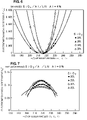
FIG. 7 shows a relationship among the electromechanical coefficient KR 2 of Rayleigh waves and the Euler angle θ and the normalized film thickness of the SiO2 film and FIG. 8 shows a relationship among the electromechanical coefficient KSH 2 of SH waves and the Euler angle θ and the normalized film thickness of the SiO2 film when the IDT electrodes made of Al have a normalized film thickness H/λ of about 8%.
FIG. 9 shows a relationship among the electromechanical coefficient KR 2 of Rayleigh waves and the Euler angle θ and the normalized film thickness of the SiO2 film and FIG. 10 shows a relationship among the electromechanical coefficient KSH 2 of SH waves and the Euler angle θ and the normalized film thickness of the SiO2 film when the IDT electrodes made of Al have a normalized film thickness of about 12%.
FIG. 11 shows a relationship among the electromechanical coefficient KR 2 of Rayleigh waves and the Euler angle θ and the normalized film thickness of the SiO2 film and FIG. 12 shows a relationship among the electromechanical coefficient KSH 2 of SH waves and the Euler angle θ and the normalized film thickness of the SiO2 film when the IDT electrodes made of Al have a normalized film thickness of about 16%.
FIG. 13 shows a relationship among the electromechanical coefficient KR 2 of Rayleigh waves and the Euler angle θ and the normalized film thickness of the SiO2 film and FIG. 14 shows a relationship among the electromechanical coefficient KSH 2 of SH waves and the Euler angle θ and the normalized film thickness of the SiO2 film when the IDT electrodes made of Al have a normalized film thickness of about 20%.
FIG. 15 shows a relationship among the electromechanical coefficient KR 2 of Rayleigh waves and the Euler angle θ and the normalized film thickness of the SiO2 film and FIG. 16 shows a relationship among the electromechanical coefficient KSH 2 of SH waves and the Euler angle θ and the normalized film thickness of the SiO2 film when the IDT electrodes made of Al have a normalized film thickness of about 24%.
As shown in FIGS. 5 to 16, as long as the Al films have a normalized film thickness in the range of about 4% to about 24% and the SiO2 films have a normalized film thickness in the range of about 20% to about 35%, the electromechanical coefficient KR 2 of Rayleigh waves has a maximum value at an Euler angle θ in the range of about 210° to about 230° irrespective of the film thickness. Furthermore, the electromechanical coefficient KR 2 tends to decrease as the Euler angle θ decreases from the angle corresponding to the maximum value, and the electromechanical coefficient KR 2 also tends to decrease as the Euler angle θ increases from the angle corresponding to the maximum value.
In contrast, the electromechanical coefficient KSH 2 of the SH waves which cause spurious responses have a minimum value in the range in which the Euler angle θ is about 200° to about 230°.
The results in FIGS. 5 to 16 show that the combinations shown in Table 9 below provide an Euler angle θ at which the main response caused by Rayleigh waves has an electromechanical coefficient KR 2 of at least about 0.08, which provides a sufficient response, and SH waves, which cause spurious responses, have an electromechanical coefficient KSH 2 of less than about 0.02. Thus, to achieve the main response caused by Rayleigh waves having an electromechanical coefficient KR 2 of at least about 0.08 and SH waves, which cause spurious responses, having an electromechanical coefficient KSH 2 of less than about 0.02, the Euler angle θ should be selected in accordance with Table 9 below.
Surface acoustic wave resonators or surface acoustic wave filters in which the main response caused by Rayleigh waves has an electromechanical coefficient KR 2 of at least about 0.08 have good resonance characteristics and filter characteristics. In this case, when SH waves have an electromechanical coefficient KSH 2 of at least about 0.02, spurious responses caused by the SH waves are no longer negligible and degrade the resonance characteristics and/or the filter characteristics.
Thus, as shown in Table 9, by selecting a combination of a normalized film thickness (%) range of the IDT electrode made of Al, a normalized film thickness (%) range of the SiO2 film, and an Euler angle θ (°) range in the rightmost column in Table 9, the main response caused by Rayleigh waves that are used has an electromechanical coefficient of at least about 0.08, which provides a sufficient response. Moreover, SH waves, which cause spurious responses, have an electromechanical coefficient of less than about 0.02, thereby effectively suppressing influences caused by spurious responses.
As shown in FIGS. 5 to 16 and Table 9, when the Euler angle θ is in the range of about 180° to about 247°, Rayleigh waves that are used have a sufficiently high electromechanical coefficient KR 2 while SH waves have a relatively low electromechanical coefficient KSH 2 by appropriately selecting the normalized film thickness of the IDT electrode and the normalized film thickness of the SiO2 film, thereby effectively suppressing spurious responses caused by the SH waves.
| TABLE 9 |
| |
| |
Thickness of SiO2 |
Cut angle achieving |
Cut angle achieving |
KR 2 > 0.08 and |
| *IDT electrode |
film |
KR 2 > 0.08 |
KSH 2 < 0.02 |
KSH 2 < 0.02 |
| |
| 2% < h/λ ≦ 6% |
17.5% < h/λ ≦ 22.5% |
210~228 |
182~240 |
210~228 |
| |
22.5% < h/λ ≦ 27.5% |
201~235 |
188~238 |
201~235 |
| |
27.5% < h/λ ≦ 32.5% |
207~229 |
205~229 |
207~229 |
| |
32.5% < h/λ ≦ 37.5% |
210~225 |
199~232 |
210~225 |
| 6% < h/λ ≦ 10% |
17.5% < h/λ ≦ 22.5% |
205~231 |
170~252 |
205~231 |
| |
22.5% < h/λ ≦ 27.5% |
204~232 |
177~243 |
204~232 |
| |
27.5% < h/λ ≦ 32.5% |
202~231 |
202~231 |
202~231 |
| |
32.5% < h/λ ≦ 37.5% |
202~232 |
194~234 |
202~232 |
| 10% < h/λ ≦ 14% |
17.5% < h/λ ≦ 22.5% |
197~239 |
170~250 |
197~239 |
| |
22.5% < h/λ ≦ 27.5% |
198~238 |
160~262 |
198~238 |
| |
27.5% < h/λ ≦ 32.5% |
194~240 |
194~236 |
194~236 |
| |
32.5% < h/λ ≦ 37.5% |
197~233 |
184~240 |
197~233 |
| 14% < h/λ ≦ 18% |
17.5% < h/λ ≦ 22.5% |
187~243 |
***Throughout the experimental range |
187~243 |
| |
22.5% < h/λ ≦ 27.5% |
181~242 |
***Throughout the experimental range |
181~242 |
| |
27.5% < h/λ ≦ 32.5% |
181~247 |
***Throughout the experimental range |
181~247 |
| |
32.5% < h/λ ≦ 37.5% |
188~236 |
***Throughout the experimental range |
188~236 |
| 18% < h/λ ≦ 22% |
17.5% < h/λ ≦ 22.5% |
180~242 |
***Throughout the experimental range |
180~242 |
| |
22.5% < h/λ ≦ 27.5% |
182~246 |
***Throughout the experimental range |
182~246 |
| |
27.5% < h/λ ≦ 32.5% |
184~238 |
***Throughout the experimental range |
184~238 |
| |
32.5% < h/λ ≦ 37.5% |
208~212 |
***Throughout the experimental range |
208~212 |
| 22% < h/λ ≦ 26% |
17.5% < h/λ ≦ 22.5% |
180~243 |
***Throughout the experimental range |
180~243 |
| |
22.5% < h/λ ≦ 27.5% |
181~240 |
***Throughout the experimental range |
181~240 |
| |
27.5% < h/λ ≦ 32.5% |
191~227 |
***Throughout the experimental range |
191~227 |
| |
32.5% < h/λ ≦ 37.5% |
**No range |
***Throughout the experimental range |
**No range |
| |
| *IDT electrode (primarily containing Al) |
| **No range achieving KR 2 > 0.08 |
| *** KSH 2 < 0.02 achieved throughout the experimental range |
Referring to Table 10 below, SH waves, which cause spurious responses, more preferably have an electromechanical coefficient KSH 2 of less than about 0.01 by selecting any combination of ranges in Table 10.
| TABLE 10 |
| |
| |
Thickness of SiO2 |
Cut angle achieving |
Cut angle achieving |
KR 2 > 0.08 and |
| *IDT electrode |
film |
KR 2 > 0.08 |
KSH 2 < 0.01 |
KSH 2 < 0.01 |
| |
| 2% < h/λ ≦ 6% |
17.5% < h/λ ≦ 22.5% |
210~228 |
191~234 |
210~228 |
| |
22.5% < h/λ ≦ 27.5% |
201~235 |
195~231 |
201~231 |
| |
27.5% < h/λ ≦ 32.5% |
207~229 |
208~225 |
208~225 |
| |
32.5% < h/λ ≦ 37.5% |
210~225 |
204~226 |
210~225 |
| 6% < h/λ ≦ 10% |
17.5% < h/λ ≦ 22.5% |
205~231 |
178~239 |
205~231 |
| |
22.5% < h/λ ≦ 27.5% |
204~232 |
187~233 |
204~232 |
| |
27.5% < h/λ ≦ 32.5% |
202~231 |
206~226 |
206~226 |
| |
32.5% < h/λ ≦ 37.5% |
202~232 |
200~228 |
202~228 |
| 10% < h/λ ≦ 14% |
17.5% < h/λ ≦ 22.5% |
197~239 |
181~238 |
197~239 |
| |
22.5% < h/λ ≦ 27.5% |
198~238 |
172~248 |
198~238 |
| |
27.5% < h/λ ≦ 32.5% |
194~240 |
200~230 |
200~230 |
| |
32.5% < h/λ ≦ 37.5% |
197~233 |
192~233 |
197~333 |
| 14% < h/λ ≦ 18% |
17.5% < h/λ ≦ 22.5% |
187~243 |
***Throughout the experimental range |
187~243 |
| |
22.5% < h/λ ≦ 27.5% |
181~242 |
***Throughout the experimental range |
181~242 |
| |
27.5% < h/λ ≦ 32.5% |
181~247 |
***Throughout the experimental range |
181~247 |
| |
32.5% < h/λ ≦ 37.5% |
188~236 |
***Throughout the experimental range |
188~236 |
| 18% < h/λ ≦ 22% |
17.5% < h/λ ≦ 22.5% |
180~242 |
***Throughout the experimental range |
180~242 |
| |
22.5% < h/λ ≦ 27.5% |
182~246 |
***Throughout the experimental range |
182~246 |
| |
27.5% < h/λ ≦ 32.5% |
184~238 |
***Throughout the experimental range |
184~238 |
| |
32.5% < h/λ ≦ 37.5% |
208~212 |
***Throughout the experimental range |
208~212 |
| 22% < h/λ ≦ 26% |
17.5% < h/λ ≦ 22.5% |
180~243 |
***Throughout the experimental range |
180~243 |
| |
22.5% < h/λ ≦ 27.5% |
181~240 |
***Throughout the experimental range |
181~240 |
| |
27.5% < h/λ ≦ 32.5% |
191~227 |
***Throughout the experimental range |
191~227 |
| |
32.5% < h/λ ≦ 37.5% |
**No range |
***Throughout the experimental range |
**No range |
| |
| *IDT electrode (primarily containing Al) |
| **No range achieving KR 2 > 0.08 |
| ***KSH 2 < 0.01 achieved throughout the experimental range |
Multiple surface acoustic wave devices were manufactured in which Y-cut X-propagation LiNbO3 substrates having various Euler angles were used, Au was used to form electrodes, the normalized film thickness h/λ(%) of the electrodes was changed in the range of about 2% to about 4%, and the normalized film thickness h/λ of the SiO2 layers was changed in the range of about 20% to about 40%. The electromechanical coefficient KR 2 of Rayleigh waves and the electromechanical coefficient KSH 2 of SH waves, which cause spurious responses against the main response of the Rayleigh waves, were measured for the surface acoustic wave devices. The results are shown in FIGS. 17 to 24.
FIG. 17 shows the electromechanical coefficient KR 2 of Rayleigh waves and FIG. 18 shows the electromechanical coefficient KSH 2 of SH waves when the IDT electrodes made of Au have a normalized film thickness (%) of about 2%.
FIGS. 17 and 18 clearly show the following finding when the IDT electrodes made of Au have a normalized film thickness of about 2%. The electromechanical coefficient KR 2 of the main response caused by Rayleigh waves is in the range of at least about 0.08 when the Euler angle θ is in the range of about 208° to about 228°, although the values depend on the thickness of the SiO2 film. The electromechanical coefficient KSH 2 of SH waves, which cause spurious responses, is in the range of less than about 0.02 when the Euler angle θ is in the range of about 203° to about 227°, although the values depend on the thickness of the SiO2 film.
FIG. 19 shows a relationship among the electromechanical coefficient KR 2 of Rayleigh waves and the Euler angle θ and the normalized film thickness of the SiO2 film and FIG. 20 shows a relationship among the electromechanical coefficient KSH 2 of SH waves and the Euler angle θ and the normalized film thickness of the SiO2 film when the IDT electrodes made of Au have a normalized film thickness H/λ of about 3%.
FIG. 21 shows a relationship among the electromechanical coefficient KR 2 of Rayleigh waves and the Euler angle θ and the normalized film thickness of the SiO2 film and FIG. 22 shows a relationship among the electromechanical coefficient KSH 2 of SH waves and the Euler angle θ and the normalized film thickness of the SiO2 film when the IDT electrodes made of Au have a normalized film thickness of about 3.5%.
FIG. 23 shows a relationship among the electromechanical coefficient KR 2 of Rayleigh waves and the Euler angle θ and the normalized film thickness of the SiO2 film and FIG. 24 shows a relationship among the electromechanical coefficient KSH 2 of SH waves and the Euler angle θ and the normalized film thickness of the SiO2 film when the IDT electrodes made of Au have a normalized film thickness of about 4%.
As shown in FIGS. 17 to 24, as long as the Au films have a normalized film thickness in the range of about 2% to about 4% and the SiO2 films have a normalized film thickness in the range of about 20% to about 40%, the electromechanical coefficient KR 2 of Rayleigh waves has a maximum value at an Euler angle θ in the range of about 208° to about 228° irrespective of film thickness. Furthermore, the electromechanical coefficient KR 2 tends to decrease as the Euler angle θ decreases, and the electromechanical coefficient KR 2 also tends to decrease as the Euler angle θ increases from the angle corresponding to the maximum value.
In contrast, the electromechanical coefficient KSH 2 of SH waves, which cause spurious responses, have a minimum value in the range in which the Euler angle θ is about 200° to about 230°.
The results in FIGS. 17 to 24 show that combinations shown in Table 11 below provide an Euler angle θ at which the main response caused by Rayleigh waves has an electromechanical coefficient KR 2 of at least about 0.08, which provides a sufficient response, and SH waves, which cause spurious responses, have an electromechanical coefficient KSH 2 of less than about 0.02. Thus, to achieve the main response caused by Rayleigh waves having an electromechanical coefficient KR 2 of at least about 0.08 and SH waves, which cause spurious responses, having an electromechanical coefficient KSH 2 of less than about 0.02, the Euler angle θ should be selected in accordance with Table 11 below.
Surface acoustic wave resonators or surface acoustic wave filters in which the main response caused by Rayleigh waves has an electromechanical coefficient KR 2 of at least about 0.08 have good resonance characteristics and filter characteristics. In this case, when SH waves have an electromechanical coefficient KSH 2 of about 0.02 or more, spurious responses caused by the SH waves are no longer negligible and degrade resonance characteristics and/or filter characteristics.
Thus, as shown in Table 11, by selecting a normalized film thickness (%) range of the IDT electrode made of Au, a normalized film thickness (%) range of the SiO2 film, and an Euler angle θ (°) range in the rightmost column in Table 11, the main response caused by Rayleigh waves that are used have an electromechanical coefficient of at least about 0.08, which provides a sufficient response. Moreover, SH waves, which cause spurious responses, have an electromechanical coefficient of less than about 0.02, to thereby effectively suppress influences caused by spurious responses.
As show in FIGS. 17 to 24 and Table 11, when the Euler angle θ is in the range of about 208° to about 225°, Rayleigh waves that are used may have a sufficiently high electromechanical coefficient KR 2 while SH waves may have a relatively low electromechanical coefficient KSH 2 by appropriately selecting the normalized film thickness of the IDT electrode and the normalized film thickness of the SiO2, thereby effectively suppressing spurious responses caused by the SH waves.
| TABLE 11 |
| |
| *Film thickness of |
Thickness of |
Cut angle achieving |
Cut angle achieving |
KR 2 > 0.08 and |
| IDT electrode |
SiO2 film |
KR 2 > 0.08 |
KSH 2 < 0.02 |
KSH 2 < 0.02 |
| |
| 1.5% < h/λ ≦ 2.5% |
17.5% < h/λ ≦ 22.5% |
208~224 |
207~224 |
208~224 |
| |
22.5% < h/λ ≦ 27.5% |
208~228 |
208~222 |
208~222 |
| |
27.5% < h/λ ≦ 32.5% |
208~228 |
207~224 |
208~224 |
| |
32.5% < h/λ ≦ 37.5% |
210~226 |
205~225 |
210~225 |
| |
37.5% < h/λ ≦ 42.5% |
**No range |
203~227 |
**No range |
| 2.5% < h/λ ≦ 3.25% |
17.5% < h/λ ≦ 22.5% |
208~228 |
209~221 |
209~221 |
| |
22.5% < h/λ ≦ 27.5% |
209~227 |
209~221 |
209~221 |
| |
27.5% < h/λ ≦ 32.5% |
209~227 |
208~223 |
209~223 |
| |
32.5% < h/λ ≦ 37.5% |
209~226 |
207~224 |
210~225 |
| |
37.5% < h/λ ≦ 42.5% |
212~224 |
204~226 |
212~224 |
| 3.25% < h/λ ≦ 3.75% |
17.5% < h/λ ≦ 22.5% |
210~226 |
***No range |
***No range |
| |
22.5% < h/λ ≦ 27.5% |
212~224 |
***No range |
***No range |
| |
27.5% < h/λ ≦ 32.5% |
212~224 |
***No range |
***No range |
| |
32.5% < h/λ ≦ 37.5% |
211~225 |
210~222 |
210~225 |
| |
37.5% < h/λ ≦ 42.5% |
212~224 |
206~225 |
212~224 |
| |
| *Film thickness of IDT electrode (primarily containing Au) |
| **No range achieving KR 2 > 0.08 |
| ***No range achieving KSH 2 < 0.02 |
Referring to Table 12 below, SH waves, which cause spurious responses, more preferably have an electromechanical coefficient KSH 2 of less than about 0.01 by selecting the Euler angle θ from the range of about 210° to about 225° and selecting the Euler angle θ, the normalized film thickness (%) of the SiO2, and the normalized film thickness (%) of the IDT electrode from the ranges shown in Table 12.
| TABLE 12 |
| |
| *Film thickness of |
Thickness of |
Cut angle achieving |
Cut angle achieving |
KR 2 > 0.08 and |
| IDT electrode |
SiO2 film |
KR 2 > 0.08 |
KSH 2 < 0.01 |
KSH 2 < 0.01 |
| |
| 1.5% < h/λ ≦ 2.5% |
17.5% < h/λ ≦ 22.5% |
208~228 |
210~224 |
210~224 |
| |
22.5% < h/λ ≦ 27.5% |
208~228 |
211~222 |
211~222 |
| |
27.5% < h/λ ≦ 32.5% |
208~228 |
210~224 |
210~224 |
| |
32.5% < h/λ ≦ 37.5% |
210~226 |
208~225 |
210~225 |
| |
37.5% < h/λ ≦ 42.5% |
**No range |
206~227 |
**No range |
| 2.5% < h/λ ≦ 3.25% |
17.5% < h/λ ≦ 22.5% |
208~228 |
214~221 |
214~221 |
| |
22.5% < h/λ ≦ 27.5% |
209~227 |
***No range |
***No range |
| |
27.5% < h/λ ≦ 32.5% |
209~227 |
214~218 |
214~228 |
| |
32.5% < h/λ ≦ 37.5% |
209~226 |
210~222 |
210~225 |
| |
37.5% < h/λ ≦ 42.5% |
212~224 |
208~223 |
212~223 |
| 3.25% < h/λ ≦ 3.75% |
17.5% < h/λ ≦ 22.5% |
210~226 |
***No range |
***No range |
| |
22.5% < h/λ ≦ 27.5% |
212~224 |
***No range |
***No range |
| |
27.5% < h/λ ≦ 32.5% |
212~224 |
***No range |
***No range |
| |
32.5% < h/λ ≦ 37.5% |
211~225 |
***No range |
***No range |
| |
37.5% < h/λ ≦ 42.5% |
212~224 |
208~222 |
212~222 |
| |
| *Film thickness of IDT electrode (primarily containing Au) |
| **No range achieving KR 2 > 0.08 |
| ***No range achieving KSH 2 < 0.01 |
Multiple surface acoustic wave devices were manufactured in which Y-cut X-propagation LiNbO3 substrates with various Euler angles were used, Cu was used to form electrodes, the normalized film thickness h/λ (%) of the electrodes was changed in the range of about 2% to about 8%, and the normalized film thickness h/λ of the SiO2 layers was changed in the range of about 20% to about 40%. The electromechanical coefficient KR 2 of Rayleigh waves and the electromechanical coefficient KSH 2 of SH waves, which cause spurious responses against the main response of the Rayleigh waves, were measured for the surface acoustic wave devices. The results are shown in FIGS. 25 to 32.
FIG. 25 shows the electromechanical coefficient KR 2 of Rayleigh waves and FIG. 26 shows the electromechanical coefficient KSH 2 of SH waves when the IDT electrodes made of Cu have a normalized film thickness (%) of about 2%.
FIGS. 25 and 26 clearly show the following finding when the IDT electrodes made of Cu have a normalized film thickness of about 2%. The electromechanical coefficient KR 2 of the main response caused by Rayleigh waves is in the range of at least about 0.08 when the Euler angle θ is in the range of about 208° to about 228°, although the values depend on the thickness of the SiO2 film. The electromechanical coefficient KSH 2 of SH waves, which cause spurious responses, is in the range of less than about 0.02 when the Euler angle θ is in the range of about 202° to about 228°, although the values depend on the thickness of the SiO2 film.
FIG. 27 shows a relationship among the electromechanical coefficient KR 2 of Rayleigh waves and the Euler angle θ and the normalized film thickness of the SiO2 film and FIG. 28 shows a relationship among the electromechanical coefficient KSH 2 of SH waves and the Euler angle θ and the normalized film thickness of the SiO2 film when the IDT electrodes made of Cu have a normalized film thickness H/λ of about 4%.
FIG. 29 shows a relationship among the electromechanical coefficient KR 2 of Rayleigh waves and the Euler angle θ and the normalized film thickness of the SiO2 film and FIG. 30 shows a relationship among the electromechanical coefficient KSH 2 of SH waves and the Euler angle θ and the normalized film thickness of the SiO2 film when the IDT electrodes made of Cu have a normalized film thickness of about 6%.
FIG. 31 shows a relationship among the electromechanical coefficient KR 2 of Rayleigh waves and the Euler angle θ and the normalized film thickness of the SiO2 film and FIG. 32 shows a relationship among the electromechanical coefficient KSH 2 of SH waves and the Euler angle θ and the normalized film thickness of the SiO2 film when the IDT electrodes made of Cu have a normalized film thickness of about 8%.
As shown in FIGS. 25 to 32, as long as the Cu films have a normalized film thickness in the range of about 2% to about 8% and the SiO2 films have a normalized film thickness in the range of about 20% to about 40%, the electromechanical coefficient KR 2 of Rayleigh waves has a maximum value at an Euler angle θ in the range of about 208° to about 228° irrespective of film thickness, the electromechanical coefficient KR 2 tends to decrease as the Euler angle θ decreases, and the electromechanical coefficient KR 2 also tends to decrease as the Euler angle θ increases from the angle corresponding to the maximum value.
In contrast, the electromechanical coefficient KSH 2 of SH waves, which cause spurious responses, have a minimum value in the range in which the Euler angle θ is about 202° to about 228°.
The results in FIGS. 25 to 32 show that combinations indicated in Table 13 below give an Euler angle θ at which the main response caused by Rayleigh waves has an electromechanical coefficient KR 2 of at least about 0.08, which provides a sufficient response, and SH waves, which cause spurious responses, have an electromechanical coefficient KSH 2 of less than about 0.02. Thus, to achieve the main response caused by Rayleigh waves having an electromechanical coefficient KR 2 of at least about 0.08 and SH waves, which cause spurious responses, having an electromechanical coefficient KSH 2 of less than about 0.02, the Euler angle θ should be selected in accordance with Table 13 below.
Surface acoustic wave resonators or surface acoustic wave filters in which the main response caused by Rayleigh waves has an electromechanical coefficient KR 2 of at least about 0.08 have good resonance characteristics and filter characteristics. In this case, when SH waves have an electromechanical coefficient KSH 2 of about 0.02 or more, spurious responses caused by the SH waves are no longer negligible and degrade resonance characteristics or filter characteristics.
Thus, as shown in Table 13, by selecting a normalized film thickness (%) range of the IDT electrode made of Cu, a normalized film thickness (%) range of the SiO2 film, and an Euler angle θ (°) range in the rightmost column in Table 13, the main response caused by Rayleigh waves that are used has an electromechanical coefficient of at least about 0.08, which provides a sufficient response. Moreover, SH waves, which cause spurious responses, have an electromechanical coefficient of less than about 0.02, thereby effectively suppressing influences caused by spurious responses.
As shown in FIGS. 25 to 32 and Table 13, when the Euler angle θ is in the range of about 204° to about 228°, Rayleigh waves that are used have a sufficiently high electromechanical coefficient KR 2 while SH waves have a relatively low electromechanical coefficient KSH 2 are provided by appropriately selecting the normalized film thickness of the IDT electrode and the normalized film thickness of the SiO2, thereby effectively suppressing spurious responses caused by the SH waves.
| TABLE 13 |
| |
| *Film thickness of |
Thickness of |
Cut angle achieving |
Cut angle achieving |
KR 2 > 0.08 and |
| IDT electrode |
SiO2 film |
KR 2 > 0.08 |
KSH 2 < 0.02 |
KSH 2 < 0.02 |
| |
| 1% < h/λ ≦ 3% |
17.5% < h/λ ≦ 22.5% |
209~227 |
207~225 |
209~225 |
| |
22.5% < h/λ ≦ 27.5% |
209~227 |
207~225 |
209~225 |
| |
27.5% < h/λ ≦ 32.5% |
209~227 |
203~226 |
209~226 |
| |
32.5% < h/λ ≦ 37.5% |
214~222 |
202~228 |
214~222 |
| |
37.5% < h/λ ≦ 42.5% |
**No range |
***No range |
****No range |
| 3% < h/λ ≦ 5% |
17.5% < h/λ ≦ 22.5% |
206~230 |
207~224 |
207~224 |
| |
22.5% < h/λ ≦ 27.5% |
206~230 |
207~225 |
207~225 |
| |
27.5% < h/λ ≦ 32.5% |
206~230 |
206~226 |
206~226 |
| |
32.5% < h/λ ≦ 37.5% |
207~229 |
201~227 |
207~227 |
| |
37.5% < h/λ ≦ 42.5% |
**No range |
***No range |
****No range |
| 5% < h/λ ≦ 7% |
17.5% < h/λ ≦ 22.5% |
202~232 |
207~224 |
207~224 |
| |
22.5% < h/λ ≦ 27.5% |
202~232 |
208~225 |
208~225 |
| |
27.5% < h/λ ≦ 32.5% |
202~232 |
206~226 |
206~226 |
| |
32.5% < h/λ ≦ 37.5% |
202~232 |
204~227 |
204~227 |
| |
37.5% < h/λ ≦ 42.5% |
204~228 |
200~228 |
204~228 |
| 7% < h/λ ≦ 9% |
17.5% < h/λ ≦ 22.5% |
202~234 |
208~224 |
208~224 |
| |
22.5% < h/λ ≦ 27.5% |
202~234 |
208~224 |
208~224 |
| |
27.5% < h/λ ≦ 32.5% |
202~234 |
207~225 |
207~225 |
| |
32.5% < h/λ ≦ 37.5% |
202~233 |
205~226 |
205~226 |
| |
37.5% < h/λ ≦ 42.5% |
204~232 |
202~228 |
204~228 |
| |
| *Film thickness of IDT electrode (primarily containing Cu) |
| **No range achieving KR 2 > 0.08 |
| ***No range achieving KSH 2 < 0.02 |
| ****No range achieving KR 2 > 0.08 and KSH 2 < 0.02 |
Referring to Table 14 below, SH waves, which cause spurious responses, more preferably have an electromechanical coefficient KSH 2 of less than about 0.01 by selecting the Euler angle θ from the range of about 204° to about 226° and selecting the Euler angle θ, the normalized film thickness (%) of the SiO2, and the normalized film thickness (%) of the IDT electrode from the ranges shown in Table 14.
| TABLE 14 |
| |
| *Film thickness of |
Thickness of |
Cut angle achieving |
Cut angle achieving |
KR 2 > 0.08 and |
| IDT electrode |
SiO2 film |
KR 2 > 0.08 |
KSH 2 < 0.01 |
KSH 2 < 0.01 |
| |
| 1% < h/λ ≦ 3% |
17.5% < h/λ ≦ 22.5% |
209~227 |
210~222 |
210~222 |
| |
22.5% < h/λ ≦ 27.5% |
209~227 |
210~222 |
210~222 |
| |
27.5% < h/λ ≦ 32.5% |
209~227 |
208~222 |
209~222 |
| |
32.5% < h/λ ≦ 37.5% |
214~222 |
206~224 |
214~222 |
| |
37.5% < h/λ ≦ 42.5% |
**No range |
202~226 |
**No range |
| 3% < h/λ ≦ 5% |
17.5% < h/λ ≦ 22.5% |
206~230 |
210~222 |
210~222 |
| |
22.5% < h/λ ≦ 27.5% |
206~230 |
210~222 |
210~222 |
| |
27.5% < h/λ ≦ 32.5% |
206~230 |
207~226 |
207~226 |
| |
32.5% < h/λ ≦ 37.5% |
207~229 |
206~224 |
207~224 |
| |
37.5% < h/λ ≦ 42.5% |
**No range |
204~224 |
**No range |
| 5% < h/λ ≦ 7% |
17.5% < h/λ ≦ 22.5% |
202~232 |
210~222 |
210~222 |
| |
22.5% < h/λ ≦ 27.5% |
202~232 |
210~222 |
210~222 |
| |
27.5% < h/λ ≦ 32.5% |
202~232 |
207~222 |
207~222 |
| |
32.5% < h/λ ≦ 37.5% |
202~232 |
208~224 |
208~224 |
| |
37.5% < h/λ ≦ 42.5% |
204~228 |
204~225 |
204~225 |
| 7% < h/λ ≦ 9% |
17.5% < h/λ ≦ 22.5% |
202~234 |
210~221 |
210~221 |
| |
22.5% < h/λ ≦ 27.5% |
202~234 |
210~221 |
210~221 |
| |
27.5% < h/λ ≦ 32.5% |
202~234 |
210~222 |
210~222 |
| |
32.5% < h/λ ≦ 37.5% |
202~233 |
208~223 |
208~223 |
| |
37.5% < h/λ ≦ 42.5% |
204~232 |
206~224 |
206~224 |
| |
| *Film thickness of IDT electrode (primarily containing Cu) |
| **No range achieving KR 2 > 0.08 |
Multiple surface acoustic wave devices were manufactured in which Y-cut X-propagation LiNbO3 substrates with various Euler angles were used, Ta was used to form electrodes, the normalized film thickness h/λ (%) of the electrodes was changed in the range of about 2% to about 5%, and the normalized film thickness h/λ of the SiO2 layers was changed in the range of about 20% to about 35%. The electromechanical coefficient KR 2 of Rayleigh waves and the electromechanical coefficient KSH 2 of SH waves, which cause spurious responses against the main response of the Rayleigh waves, were measured for the surface acoustic wave devices. The results are shown in FIGS. 33 to 40.
FIG. 33 shows the electromechanical coefficient KR 2 of Rayleigh waves and FIG. 34 shows the electromechanical coefficient KSH 2 of SH waves when the IDT electrodes made of Ta have a normalized film thickness (%) of about 2%.
FIGS. 33 and 34 clearly show the following finding when the IDT electrodes made of Ta have a normalized film thickness of about 2%. The electromechanical coefficient KR 2 of the main response caused by Rayleigh waves is in the range of at least about 0.08 when the Euler angle θ is in the range of about 208° to about 228°, although the values depend on the thickness of the SiO2 film. The electromechanical coefficient KSH 2 of SH waves, which cause spurious responses, is in the range of less than about 0.02 when the Euler angle θ is in the range of about 204° to about 226°, although the values depend on the thickness of the SiO2 film.
FIG. 35 shows a relationship among the electromechanical coefficient KR 2 of Rayleigh waves and the Euler angle θ and the normalized film thickness of the SiO2 film and FIG. 36 shows a relationship among the electromechanical coefficient KSH 2 of SH waves and the Euler angle θ and the normalized film thickness of the SiO2 film when the IDT electrodes made of Ta have a normalized film thickness H/λ of about 3%.
FIG. 37 shows a relationship among the electromechanical coefficient KR 2 of Rayleigh waves and the Euler angle θ and the normalized film thickness of the SiO2 film and FIG. 38 shows a relationship among the electromechanical coefficient KSH 2 of SH waves and the Euler angle θ and the normalized film thickness of the SiO2 film when the IDT electrodes made of Ta have a normalized film thickness of about 4%.
FIG. 39 shows a relationship among the electromechanical coefficient KR 2 of Rayleigh waves and the Euler angle θ and the normalized film thickness of the SiO2 film and FIG. 40 shows a relationship among the electromechanical coefficient KSH 2 of SH waves and the Euler angle θ and the normalized film thickness of the SiO2 film when the IDT electrodes made of Ta have a normalized film thickness of about 5%.
As shown in FIGS. 33 to 40, as long as the Ta films have a normalized film thickness in the range of about 2% to about 5% and the SiO2 films have a normalized film thickness in the range of about 20% to about 35%, the electromechanical coefficient KR 2 of Rayleigh waves has a maximum value at an Euler angle θ in the range of about 208° to about 228° irrespective of film thickness. Furthermore, the electromechanical coefficient KR 2 tends to decrease as the Euler angle θ decreases, and the electromechanical coefficient KR 2 also tends to decrease as the Euler angle θ increases from the angle corresponding to the maximum value.
In contrast, the electromechanical coefficient KSH 2 of SH waves, which cause spurious responses, have a minimum value in the range in which the Euler angle θ is about 202° to about 228°.
The results in FIGS. 33 to 40 show that combinations indicated in Table 15 below provide an Euler angle θ at which the main response caused by Rayleigh waves has an electromechanical coefficient KR 2 of at least about 0.08, which provides a sufficient response, and SH waves, which cause spurious responses, have an electromechanical coefficient KSH 2 of less than about 0.02. Thus, to achieve the main response caused by Rayleigh waves having an electromechanical coefficient KR 2 of at least about 0.08 and SH waves, which cause spurious responses, having an electromechanical coefficient KSH 2 of less than about 0.02, the Euler angle θ should be selected in accordance with Table 15 below.
Surface acoustic wave resonators or surface acoustic wave filters in which the main response caused by Rayleigh waves has an electromechanical coefficient KR 2 of at least about 0.08 have good resonance characteristics and filter characteristics. In this case, when SH waves have an electromechanical coefficient KSH 2 of about 0.02 or more, spurious responses caused by the SH waves are no longer negligible and degrade resonance characteristics or filter characteristics.
Thus, as shown in Table 15, by selecting a normalized film thickness (%) range of the IDT electrode made of Ta, a normalized film thickness (%) range of the SiO2 film, and an Euler angle θ (°) range in the rightmost column in Table 15, the main response caused by Rayleigh waves that are used has an electromechanical coefficient of at least about 0.08, providing a sufficient response, while SH waves, which cause spurious responses, have an electromechanical coefficient of less than about 0.02, thereby effectively suppressing influences caused by spurious responses.
As shown in FIGS. 33 to 40 and Table 15, when the Euler angle θ is in the range of about 206° to about 226°, Rayleigh waves that are used have a sufficiently high electromechanical coefficient KR 2 while SH waves have a low electromechanical coefficient KSH 2 by appropriately selecting the normalized film thickness of the IDT electrode and the normalized film thickness of the SiO2, thereby effectively suppressing spurious responses caused by the SH waves.
| TABLE 15 |
| |
| Film thickness of |
|
|
Cut angle |
|
| IDT electrode (mainly |
Cut angle achieving |
Cut angle achieving |
achieving |
KR 2 > 0.08 and |
| containing Ta) |
KR 2 > 0.08 |
KR 2 > 0.08 |
KSH 2 < 0.02 |
KSH 2 < 0.02 |
| |
| 1.5% < h/λ ≦ 2.5% |
17.5% < h/λ ≦ 22.5% |
208~228 |
206~224 |
208~224 |
| |
22.5% < h/λ ≦ 27.5% |
208~228 |
206~225 |
208~225 |
| |
27.5% < h/λ ≦ 32.5% |
208~228 |
205~226 |
208~226 |
| |
32.5% < h/λ ≦ 37.5% |
210~224 |
202~228 |
210~224 |
| 2.5% < h/λ ≦ 3.5% |
17.5% < h/λ ≦ 22.5% |
206~230 |
206~224 |
206~224 |
| |
22.5% < h/λ ≦ 27.5% |
206~230 |
206~224 |
206~224 |
| |
27.5% < h/λ ≦ 32.5% |
207~229 |
206~225 |
207~225 |
| |
32.5% < h/λ ≦ 37.5% |
208~228 |
204~226 |
208~226 |
| 3.5% < h/λ ≦ 4.5% |
17.5% < h/λ ≦ 22.5% |
204~230 |
207~224 |
207~224 |
| |
22.5% < h/λ ≦ 27.5% |
206~230 |
207~224 |
207~224 |
| |
27.5% < h/λ ≦ 32.5% |
207~229 |
209~224 |
209~224 |
| |
32.5% < h/λ ≦ 37.5% |
207~229 |
205~226 |
207~226 |
| 4.5% < h/λ ≦ 5.5% |
17.5% < h/λ ≦ 22.5% |
204~232 |
207~223 |
207~223 |
| |
22.5% < h/λ ≦ 27.5% |
205~230 |
207~223 |
207~223 |
| |
27.5% < h/λ ≦ 32.5% |
206~230 |
207~224 |
207~224 |
| |
32.5% < h/λ ≦ 37.5% |
206~230 |
207~225 |
207~225 |
| |
Referring to Table 16 below, SH waves, which cause spurious responses, more preferably have an electromechanical coefficient KSH 2 of less than about 0.01 by selecting the Euler angle θ in the range of about 208° to about 224° and by selecting the Euler angle θ, the normalized film thickness (%) of the SiO2, and the normalized film thickness (%) of the IDT electrode from the ranges shown in Table 16.
| TABLE 16 |
| |
| Film thickness of |
|
|
|
|
| IDT electrode (mainly |
Thickness of |
Cut angle achieving |
Cut angle achieving |
KR 2 > 0.08 and |
| containing Ta) |
SiO2 film |
KR 2 > 0.08 |
KSH 2 < 0.01 |
KSH 2 < 0.01 |
| |
| 1.5% < h/λ ≦ 2.5% |
17.5% < h/λ ≦ 22.5% |
208~228 |
209~222 |
209~222 |
| |
22.5% < h/λ ≦ 27.5% |
208~228 |
209~222 |
209~222 |
| |
27.5% < h/λ ≦ 32.5% |
208~228 |
208~222 |
208~222 |
| |
32.5% < h/λ ≦ 37.5% |
210~224 |
204~224 |
210~224 |
| 2.5% < h/λ ≦ 3.5% |
17.5% < h/λ ≦ 22.5% |
206~230 |
210~221 |
210~221 |
| |
22.5% < h/λ ≦ 27.5% |
206~230 |
210~221 |
210~221 |
| |
27.5% < h/λ ≦ 32.5% |
207~229 |
209~222 |
209~222 |
| |
32.5% < h/λ ≦ 37.5% |
208~228 |
208~223 |
208~223 |
| 3.5% < h/λ ≦ 4.5% |
17.5% < h/λ ≦ 22.5% |
204~230 |
210~221 |
210~221 |
| |
22.5% < h/λ ≦ 27.5% |
206~230 |
210~221 |
210~221 |
| |
27.5% < h/λ ≦ 32.5% |
207~229 |
210~222 |
210~222 |
| |
32.5% < h/λ ≦ 37.5% |
207~229 |
208~222 |
208~222 |
| 4.5% < h/λ ≦ 5.5% |
17.5% < h/λ ≦ 22.5% |
204~232 |
210~221 |
210~221 |
| |
22.5% < h/λ ≦ 27.5% |
205~230 |
211~221 |
211~221 |
| |
27.5% < h/λ ≦ 32.5% |
206~230 |
211~221 |
211~221 |
| |
32.5% < h/λ ≦ 37.5% |
206~230 |
210~222 |
210~222 |
| |
Although LiNbO3 substrates with Euler angles (0°, θ, 0°) were used in the experiments in the preferred embodiments described above, φ and ψ of the Euler angles are not necessarily restricted to 0°. Results similar to the experimental results are obtained when φ and ψ are in the range of about 0°±5°. In summary, LiNbO3 substrates in preferred embodiments of the present invention preferably have Euler angles in the range of (0°±5°, 180° to 247°, 0°±5°).
Although the IDT electrode 3 was made of Al, Au, Cu, or Ta in the preferred embodiments described above, preferred embodiments of the present invention are not limited thereto as long as a metal primarily including Al, Au, Cu, or Ta is used. The IDT electrode 3 may preferably be made of an alloy primarily including Al, Au, Cu, or Ta, for example. The metal primarily including Al may preferably be a multilayer metal film including a metal film primarily including Al, Au, Cu, or Ta and a metal film made of a metal or an alloy having a higher density than Al. Examples of such a metal or an alloy having a higher density than Al may include Ti, Ni, Cr, NiCr, and AlCu. Alternatively, another multilayer metal film may be used that includes a metal film primarily including Al, Au, Ta, or Cu and Al or an alloy primarily including Al disposed on the metal film.
While preferred embodiments of the present invention have been described above, it is to be understood that variations and modifications will be apparent to those skilled in the art without departing the scope and spirit of the present invention. The scope of the present invention, therefore, is to be determined solely by the following claims.