US7541964B2 - Analogue/digital converter microelectronic device for equalising charges - Google Patents
Analogue/digital converter microelectronic device for equalising charges Download PDFInfo
- Publication number
- US7541964B2 US7541964B2 US11/749,479 US74947907A US7541964B2 US 7541964 B2 US7541964 B2 US 7541964B2 US 74947907 A US74947907 A US 74947907A US 7541964 B2 US7541964 B2 US 7541964B2
- Authority
- US
- United States
- Prior art keywords
- charge
- state
- injector
- injection
- signal
- Prior art date
- Legal status (The legal status is an assumption and is not a legal conclusion. Google has not performed a legal analysis and makes no representation as to the accuracy of the status listed.)
- Active, expires
Links
Images


Classifications
-
- H—ELECTRICITY
- H03—ELECTRONIC CIRCUITRY
- H03M—CODING; DECODING; CODE CONVERSION IN GENERAL
- H03M1/00—Analogue/digital conversion; Digital/analogue conversion
- H03M1/12—Analogue/digital converters
- H03M1/18—Automatic control for modifying the range of signals the converter can handle, e.g. gain ranging
-
- G—PHYSICS
- G01—MEASURING; TESTING
- G01T—MEASUREMENT OF NUCLEAR OR X-RADIATION
- G01T1/00—Measuring X-radiation, gamma radiation, corpuscular radiation, or cosmic radiation
- G01T1/16—Measuring radiation intensity
- G01T1/17—Circuit arrangements not adapted to a particular type of detector
-
- H—ELECTRICITY
- H04—ELECTRIC COMMUNICATION TECHNIQUE
- H04N—PICTORIAL COMMUNICATION, e.g. TELEVISION
- H04N25/00—Circuitry of solid-state image sensors [SSIS]; Control thereof
- H04N25/50—Control of the SSIS exposure
- H04N25/57—Control of the dynamic range
-
- H—ELECTRICITY
- H04—ELECTRIC COMMUNICATION TECHNIQUE
- H04N—PICTORIAL COMMUNICATION, e.g. TELEVISION
- H04N25/00—Circuitry of solid-state image sensors [SSIS]; Control thereof
- H04N25/70—SSIS architectures; Circuits associated therewith
- H04N25/76—Addressed sensors, e.g. MOS or CMOS sensors
- H04N25/78—Readout circuits for addressed sensors, e.g. output amplifiers or A/D converters
-
- H—ELECTRICITY
- H03—ELECTRONIC CIRCUITRY
- H03M—CODING; DECODING; CODE CONVERSION IN GENERAL
- H03M1/00—Analogue/digital conversion; Digital/analogue conversion
- H03M1/12—Analogue/digital converters
- H03M1/60—Analogue/digital converters with intermediate conversion to frequency of pulses
Definitions
- the invention relates to the field of microelectronic imaging sensors or image sensors, especially using CMOS technology.
- the invention relates to a microelectronic device equipped with one or more pixels, comprising respectively, a detector and an analogue/digital converter, especially asynchronous and with modulable charge injection.
- the invention also relates to a method for commanding such a device.
- the invention permits in particular to obtain improved conversion dynamics.
- a microelectronic imaging device or image sensor is generally formed by a matrix of pixels and an electronic control device.
- Each pixel comprises a detector, equipped for example with at least one photodiode or at least one phototransistor, provided to convert the energy of the incident photons on the pixel into electrons-hole couples, with an integration capacity, whose role is to stock these charges, as well as one or more transistors.
- the pixel matrix supplies an analogue signal, which the command device can convert into a digital signal.
- the analogue/digital conversion may possibly be carried out inside the chip in which the pixel matrix is integrated.
- FIG. 1 A microelectronic digitising device revealed in this document is illustrated in FIG. 1 .
- This digitising device is formed by a synchronous modulator ⁇ 2 , comprising an integration capacitor 1 designed to receive the charges, in the form of a current Idet, issued from the photo-detector, a comparator 3 driven by a clock 4 .
- the comparator 3 commands a charge injector 6 connected to an output of the comparator 3 and designed to inject charge packets into the capacitor 1 , as an input to the comparator 3 .
- the modulator ⁇ 2 issues a bit stream which may be filtered using a digital filter 8 , for example a decimating filter located outside of a chip into which the pixel matrix and the digitising device are integrated.
- a digital filter 8 for example a decimating filter located outside of a chip into which the pixel matrix and the digitising device are integrated.
- Such a digitising device typically has good linearity, but in general only allows a relatively low resolution to be achieved.
- FIG. 1 Another type of analogue digital converter device, called a “charge balancing” device, integrated into an imager is described in the document: “A 64-channel wide dynamic range charge measurement ASIC for strip and pixel ionization detectors”, Mazza and al., IEEE, trans. On nuclear science vol. 52 n o 4 August 2005.
- This device comprises an integration capacitor 10 at the output of a detector 11 that is connected to an input of a comparator 13 , as well as a charge injector 19 .
- FIG. 1 One operating mode of this digitising device is illustrated in FIG.
- the analogue signal or the voltage Vint reaches a certain threshold, for example it passes below a threshold voltage Vthreshold of the comparator 13 .
- the signal Scomp at the output of the comparator 13 switches. During this switch, the signal Scomp at the output of the comparator 13 passes from a first state called a “stable” state, for example a high state, to a second state, for example a low state.
- a switch is shown, for example by a front descending edge 23 in FIG. 4A .
- the change of state of the signal Scomp triggers an injection, by the injector 19 , of a quantity of fixed charges Q 0 .
- Such an injection of charge may cause for example an increase in the signal Vint (vertical portion of the curve referenced 24 in FIG. 4A ) of a value of around Q o /C.
- the increase in the signal Vint caused by the injection is such that this signal Vint reaches a value higher than the threshold voltage of the comparator 13 and that is sufficient to permit the output of the comparator to switch again or at the signal Scomp to pass from the second state to the first state (front edge reference 25 ) or to switch to the stable state.
- the signal Scomp at the output of the comparator 13 returns to its stable state or switches back to the first state after each charge injection.
- the number of injections that the injector 19 performs to balance the charges issued from the detector 11 enables a digital value to be attributed which is representative of the quantity of total charges issued from the detector 11 .
- the digitising is sensitive to the rapidity of the comparator 13 , which can, if it is too slow, for example if the time constant ⁇ is such that: ⁇ >(Q o /I DET ), block a digitising in progress.
- Such a blockage is illustrated in FIG. 4B (portion 31 of the curve which represents the output signal Scomp of the comparator blocked in the second state or in the low state).
- the invention relates firstly to a microelectronic device comprising: at least one detector formed, of at least one integration capacitor associated to the detector and capable of providing at least one analogue signal that is likely to vary at least according to a current supplied by the detector, and analogue/digital conversion means comprising:
- the microelectronic device may be an image sensor.
- the detector may be formed by at least one photo-detector element.
- the command means of the charge injector means may be provided to receive the two-states signal.
- the invention permits a wider conversion dynamic to be obtained.
- the invention avoids having to provide for, before or during the acquisition of an image, which range light intensity or which calibre has to be used.
- the charge injector means may be formed by a plurality of charge injectors.
- the charge injector means may be in the form of at least one transistor commanded by a voltage.
- the command means of the injector means are likely to modulate the given quantity of charge Qc by varying said voltage applied to said transistor.
- command means may be provided to activate a first charge injector or a first plurality of charge injectors to carry out a first injection of charge of a given value, and to activate a different injector from the first injector or a plurality of injectors different from the first plurality of injectors, to make at least one other injection of charge of a value equal to said given value.
- the charge injector means are formed by a plurality of charge injectors, and in which command means are provided so that, at each injection of charge of a series of charge injections, the command means activate at least one or more different injector(s) from the charge injector or charge injectors activated during the previous charge injection.
- the invention can also permit the effects of technological dispersions to be limited.
- the injector means may be formed by a plurality of identical injectors, respectively capable of injecting a fixed quantity of elementary charge Qo.
- the microelectronic image sensor device of the invention may possibly further comprise: counting means comprising a plurality of flip-flops, wherein the command means of the charge injector means, are capable of triggering, for each charge injection Qc, a modification of the output of at least one given flip-flop selected from said flip-flops, wherein said given flip-flop is selected according to the quantity of charges Qc injected.
- command means may be provided to adapt the quantity of charge Qc designed to be injected during at least one given charge injection, at least according to a frequency of charge injections made prior to said given charge injection.
- command means may be provided to adapt the quantity of charge Qc designed to be injected during at least one given charge injection, at least according to a minimum level of said analogue signal.
- the microelectronic image sensor device of the invention may comprise means forming a monostable capable of:
- Such means permit to avoid a blockage of the conversion, especially when the detection current is high.
- command means may be provided moreover so that: if the number of trigger orders reaches a predetermined threshold and the signal at the output of the comparator remains in the second state, the quantity of charge Qc is increased at least for one further charge injection.
- command means may be provided moreover so that: if the number of trigger orders following said change of state is less than or equal to a predetermined threshold when the signal at the output of the comparator switches back to the first state, the quantity of charge Qc is decreased at least for one further charge injection.
- analogue/digital converter means may not be fitted with a clock or may be asynchronous.
- the invention also relates to a method for commanding a microelectronic device comprising at least one detector, at least one integration capacitor associated to the detector and capable of supplying at least one analogue signal likely to vary at least according to a current supplied by the detector, wherein the method comprises steps consisting of:
- said estimation of the current supplied by the detector may be made at least using one parameter of said analogue signal.
- Said estimation may possibly be made at least according to a frequency of charge injections Qc.
- said estimation may be made at least according to the minimum level of the analogue signal.
- the method may comprise among others, following said change of state the step consisting of:
- the method may further comprise: an increase in the quantity of charge for at least one following charge injection.
- the method may further comprise: a reduction in the quantity of charge injected for at least one following charge injection.
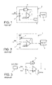
- FIG. 1 illustrates a first example of the device of the prior art, equipped with a synchronous analogue digital converter and with charge injections, integrated into a pixel matrix of an imager or an image sensor,
- FIG. 2 illustrates a second example of device of the prior art, equipped with an asynchronous analogue digital converter, integrated into a pixel matrix of an imager or an image sensor,
- FIG. 3 illustrates a third example of device of the prior art, equipped with an asynchronous analogue digital converter and with charge injections, integrated into a pixel matrix of an imager or an image sensor,
- FIGS. 4A and 4B respectively illustrate, using input and output signals of a comparator that is part of the third example of the device of the prior art, normal operation of this device and blocking of a digitising embodiment with this device,
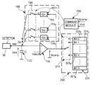
- FIG. 5 illustrates an example of an analogue digital conversion device of the invention, integrated into a pixel of an imager, and equipped in particular with charge injector means, with modulable charge injection,
- FIGS. 6A , 6 B illustrate a modulation of the counter charge Qc injected by a charge injector charges of a digitising device of the invention
- FIG. 7 illustrates another example of an analogue digital conversion device of the invention, integrated into a pixel of an imager, and equipped in particular with retriggering means designed to prevent blockage of the conversion device,
- FIG. 8 illustrates an example of saturation, that the retriggering means of an analogue digital conversion device of the invention are likely to prevent
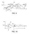
- FIG. 9 illustrates an example of adaptation or modulation of the quantity of charges injected by the charge injector means in an analogue digital conversion device of the invention, integrated into at least one pixel of an imager,
- FIG. 10 illustrates another example of adaptation or modulation of the quantity of charges injected by the charge injector means in an analogue digital conversion device of the invention, integrated into at least one pixel of an imager,
- FIG. 5 One example of a digitising device or analogue/digital conversion, of the invention, belonging to a microelectronic imaging device or image sensor, is illustrated in FIG. 5 .
- the digitising device is associated to a detector 50 of a pixel of the device image sensor.
- the digitising device and the detector may be integrated into a same pixel and/or to a same chip and/or a same support and/or may belong to a same integrated circuit.
- the detector may be assembled or hybridized on the digitising device.
- the detector 50 may comprise at least one photo-detector element, for example at least one photodiode or at least one phototransistor (not shown in FIG. 5 ), provided to convert the incident photon energy on the pixel in electron-hole pairs.
- the photo-detector element may be provided to detect an electromagnetic radiation, which may for example be visible or X ray or infrared.
- an integration capacitor 110 of capacity C designed to receive charges issued by the detector 50 in the form of a detection current Idet.
- the current Idet issued from the detector 50 may be for example between 100 fA and 20 nA.
- an analogue signal in the form of a voltage Vint varies especially according to the detection current Idet, wherein the detection current Idet is itself dependent or a function of a luminous intensity or of a quantity of photons received by the detector 50 .
- the digitising device is of the “charge equalising” type and further comprises a comparator 130 , charge injector means 190 , counting means 200 at the output of the comparator 130 , as well as a command module 250 for the charge injector means 190 and counting means 200 .
- the comparator 130 is designed to receive the analogue signal Vint on one of its inputs, and is provided to compare this signal Vint with a threshold voltage Vseuil. The result of this comparison is produced at the output of the comparator 130 , in the form of a two states signal referenced Scomp, likely to adopt a first state called the “stable state”, which may be for example a high state, or a second state which may be for example a low state.
- the comparator 130 may have a time constant ⁇ for example of around 100 ns.
- the digital signal in two states Scomp is supplied in particular to the counting means 200 .
- the counting means 200 are located at the output of the comparator 130 and comprise means forming a switch or a switching device 210 as well as means forming a counter 220 .
- the counter 220 may be formed by a plurality of flip-flops, for example by N flip-flops 221 0 , 221 1 , . . . , 221 k , . . . , 221 N-1 (where k and N are integers).
- the switch 210 is provided to connect the output of the comparator 130 to at least one flip-flop selected from the plurality of flip-flops 221 0 , 221 1 , . . . , 221 k , . . .
- the output of the counter 220 is designed to, indicate the result of the analogue-digital conversion.
- the outputs of the flip-flops 221 0 , 221 1 , . . . , 221 k , . . . , 221 N-1 are respectively associated to one bit of a plurality of bits Bit 0 , . . . , BitN-1.
- the charge injector means 190 are located between the output of the comparator 130 and the integration capacitor 110 . These charge injector means 190 are capable, following a variation of the current Idet, of injecting a quantity of charges Qc or a series of quantities of charges Qc into the integration capacitor 110 .
- Charge injector means 190 are provided to modify the analogue signal Vint by one or more injections, respectively by a given quantity of charges Qc, in the capacitor 110 following a change of state at the output of the comparator 130 , from the first state to the second state.
- the quantity of charges also called “counter charge” Qc injected by the means 190 may be variable and adapted to suit the intensity of the current Idet.
- the counter charge Qc is preferably such that: Qc>Idet* ⁇ .
- the charge injector means 190 may be in the form of a plurality of m (where m>0) charge injectors 191 1 , . . . , 191 m respectively comprising: charge storage means 193 associated to means forming a switch 195 .
- the counter charge Qc is the sum of the charges issued from the injectors selected from said plurality of injectors 191 1 , . . . , 191 m .
- Charge injector means 190 may be formed by a plurality of charge injectors 191 1 , . . . , 191 m , identical to one another.
- Charge storage means 193 may be suitable, respectively, for storing a fixed quantity of elementary charge Q 0 when the switch means 195 to which these storage means 193 are associated, are blocked or open or in a state called “deactivated”.
- the fixed elementary charge Q 0 may be for example around 2000 holes or 0.32 fC.
- the charge storage means 193 are respectively capable of providing the quantity of fixed elementary charge Q 0 when the respective switch means 195 to which these storage means 193 are associated, are open or closed or in an “activated” state.
- the quantity of charges or the counter charge Qc injected may be variable from one charge injection to another.
- the number p of charge injectors activated or selected from the m charge injectors 191 1 , . . . , 191 m may thus be variable from one charge injection to another.
- activated injector we mean an injector providing a quantity of fixed charge Q 0 whose associated switch is activated or closed or open.
- the device is equipped with means to adapt the counter charge Qc issued from the charge injector means 190 .
- This counter charge Qc may be adapted or modulated to suit the intensity of the current Idet issued from the detector 50 .
- the injector means may provide a quantity of charge Qc for example equal to Q 0 , using an activated injector 191 1 , then, during the following injection, provide a quantity of charge Qc for example equal to 2*Q 0 , using two activated injectors 191 1 , 191 2 .
- the digitising device may be used so that the activated injectors change from one charge injection to another, or from one injection to the following injection.
- the device may be provided in particular so that, during a succession of charge injections, it activates a first charge injector or a first plurality of charge injectors to make a first charge injection of a given value, and to activate a different injector than the first injector or a plurality of injectors different from the first plurality of injectors, to make at least another charge injection of a value equal to said given value.
- Said first injection and said other injection may be successive.
- the device may be used so that during one series of charge injections made by the injector means 190 , at each charge injection, at least one charge injector or several charge injectors, or all the charge injectors, are different from that or those selected from the previous charge injection.
- the injector means 190 are capable of providing a quantity of charge Qc for example equal to Q 0 , using a first activated injector 191 1 then, during the following injection, of providing a quantity of charge Qc for example equal to Q 0 , using a second activated injector 191 2 , that is different from the first injector 191 1 .
- the command module 250 receives at its input, the two-states signal Scomp from the output of the comparator 130 , as well as the signal Vint at the terminals of the integration capacitor 110 .
- the selection for each injection, of the injector(s) 191 1 , . . . , 191 m designed to provide the counter charge Qc in the capacitor 110 is made by the command module 250 .
- the command module 250 in particular may be used, for example using at least one offset register, to select, for an injection or for each injection made by the injector means 190 , at least an injector that is different from the injectors or the injector selected during the previous injection.
- the command module 250 is also provided, to select for each injection, a number p of injectors adapted to suit the evolution of the signal Vint.
- the command module 250 may also be provided to control the switches of the switching device 210 .
- the command module 250 can make a selection, via the switch 210 , of an input from the counter 220 from the counter inputs 220 , to be connected to the output of the comparator 130 .
- the command module 250 is therefore capable of triggering a connection of an input of a flip-flop from the flip-flop inputs 211 0 , 211 1 , . . . , 211 k , . . .
- the selection of a flip-flop among the flip-flops 211 0 , 211 1 , . . . , 211 k , . . . , 211 N-1 is made according to the value of the counter charge Qc provided for this given charge injection.
- the selection of one or more injectors may be made simultaneously to that of one or more flip-flops of the counting means 200 .
- the command module 250 is thus capable of triggering, for each charge injection, a modification of the output of at least one given flip-flop selected from said flip-flops, wherein the given flip-flop is selected according to the value of the counter charge Qc injected.
- the counter 220 contains the digital value of the quantity of charge received at the input of the device or the current Idet.
- the accuracy or least significant bit of the counter 220 is determined according to the value of the last counter charge Qc injected during said conversion. In one case for example, where the last injection made during a conversion is equal to Q 0 , the N bits bit 0 , . . . , bit N-1 of the counter 220 are significant. In another case for example, where the last injection made during a conversion is equal to 2*Q 0 , N-1 bits of the counter 220 are significant. In another case for example, where the last injection made during a conversion is equal to (2 k )*Q 0 , N-K bits of the counter 220 are significant.
- the adaptation of the value of the counter charge Qc for an injection may be made by this command module 250 according to the signal Vint and in particular the frequency F of the injections in this signal Vint.
- An estimation of the frequency F of the injections may permit an estimation of the current Idet issued from the detector to be made.
- the command module 250 may be used so that when the frequency of the injections F exceeds a first predetermined threshold F seuil — timber , such that F seuil — teeth ⁇ 1/ ⁇ , the counter charge Qc is increased, for example doubled, at least for the following charge injection and possibly for the following charge injections.
- the counter charge current injected is equal to 2*Q 0 ( FIG. 6A , wherein an example of the analogue signal Vint at the input of the comparator 130 is shown in this figure) and the frequency of the injections F reaches or exceeds the first given threshold F seuil — lamb
- the command module 250 may select two additional injectors for the following charge injection so that the next counter charge is equal to 4*Q 0 ( FIG.
- a second threshold may also be used so that when the frequency of the injections F reaches or drops below a second given threshold F seuil — bas , the counter charge Qc is reduced, for example halved.
- the command module 250 may select two injectors less for the following charge injection so that the following counter charge is equal to 2*Q 0 ( FIG. 6A ).
- the adaptation of the number p of injectors selected by the command module 250 or the value of the counter charge Qc injected may be according to the value or the amplitude of the integration voltage Vint.
- the adaptation of the counter charge Qc may be made in particular according to the minimum Vmin reached by the integration voltage Vint following a discharge of the integration capacitor 110 .
- the minimum value Vmin of the integration voltage Vint provides an indication to the command module 250 of the value of the product Idet* ⁇ .
- An estimation of the minimum value Vmin of the integration voltage Vint may permit an estimation of the current Idet issued from the detector to be made, and permit the command module 250 to adapt the value of the following counter charge Qc to suit the value of the product Idet* ⁇ .
- the device of the invention is not limited to injector means formed by injectors that are identical to one another. Nor is the invention limited to counter charge values Qc which follow a progression in 2 i .
- the counting means may comprise a counter whose increment is 3, and formed, for example, using at least one adder.
- the microelectronic device of the invention is not limited to injector means formed by a plurality of injectors.
- the charge injector means may for example be in the form of a transistor commanded by a voltage, wherein the command means of the injector means are capable of modulating the quantity of charge Qc by modulating said voltage applied to said transistor.
- FIG. 7 One variant of the digitising device of the invention previously described, is illustrated in FIG. 7 .
- the digitising device is equipped moreover with means forming a monostable 300 called “retriggering” located at the output of the comparator 130 , between the latter and the counting means 250 .
- the monostable 300 supplies a two-states signal Smono, and does not have a clock and/or asynchronous operation.
- the digitising embodiment via the converter is only slightly sensitive to the rapidity of the comparator 130 or to the delay ⁇ for triggering the comparator 130 , and permits to guard against a blockage as shown in FIG.
- the monostable 300 may be formed for example by a flip-flop designed to receive the output signal Scomp from the comparator 130 , of several delay cells, as well as one or more logic gates.
- the monostable 300 comprises in particular means for:
- the command module 250 is replaced by another command module referenced 350 .
- the command module 350 of this variant of device receives at its input the output signal Scomp of the comparator 130 , as well as the output signal Smono of the monostable 300 .
- the command module 350 is provided to select, when it receives an injection trigger instruction or an injection trigger command from the monostable 300 , the injector(s) 191 1 , . . . , 191 m designed to provide the quantity of charges Qc in the capacitor 110 .
- the command module 350 is also capable of selecting for each injection of counter-charge Qc, an input from a flip-flop from the inputs of the flip-flops 211 0 , 211 1 , . . .
- the monostable 300 has a time constant ⁇ ′.
- the time constant ⁇ ′ may be for example around 60 nanoseconds and correspond to a minimum duration between two injection trigger instructions or between two injection trigger commands.
- the device of the invention is used to guard against saturation when Idet* ⁇ ′>Q 0 , such a saturation is illustrated for example in FIG. 8 .
- the command module 350 may be used to count down the number Xi of consecutive trigger instructions or trigger commands in the signal Smono, following a change of state, from the first state to the second state, of the signal Scomp at the output of the comparator 130 .
- An estimation of the number Xi of trigger instructions can permit an estimation of the current Idet issued from the detector to be made.
- Too high a number Xi of consecutive trigger instructions or trigger commands can indicate to the command unit 350 that the counter charge Qc should preferably be increased, whilst too few a number Xi of consecutive trigger instructions or trigger commands can indicate to the command unit 350 that the counter charge Qc should preferably be reduced.
- the command module 350 counts down the number Xi of prior consecutive trigger instructions or trigger commands. In a case where the number Xi of trigger instructions reaches a first predetermined threshold Seuil_max, for example 4 triggers, whilst the output signal Scomp of the comparator remains in the second state, the command module 350 increases the value of the counter charge Qc for the following charge injection.
- the command module 350 reduces the value of the counter charge Qc for the following charge injection.
- a first charge injection portion referenced 401 of the curve 400 is made via the injector means 190 with a counter charge Qc equal to Q 0 .
- a first charge injection (portion referenced 451 of the curve 450 ) is made by the injector means 190 with a counter charge Qc equal to 2*Q 0 .
- the first charge injection at the moment t 0 is sufficient to switch the output signal Scomp of the comparator 130 back to the second state or stable state.
- the command unit 350 reduces the counter charge for the following charge injection. Then, at a moment t 1 , a second charge injection (portion referenced 452 of the curve 450 ) is made with a reduced counter charge Qc equal to Q 0 .
- the invention permits an improved conversion dynamic to be obtained whilst conserving good accuracy.
- the photo detector 50 In a case for example where the photo detector 50 is lit for a duration ⁇ t, the latter produces a current Idet which may be high and which would require a change in the operating range of the image sensor.
- the injector means 190 in response to this high current Idet may then inject counter charges Qc equal for example to 8*Q 0 .
- the photo detector 50 is no longer lit, so that the current Idet falls to a very low value, for example that of the obscurity current.
- the device then adapts the value of the counter charges injected Qc to the value of the fixed elementary charge Q 0 . An accuracy of Q 0 may be achieved in spite of the change in range that has just been made.
Landscapes
- Engineering & Computer Science (AREA)
- Signal Processing (AREA)
- Multimedia (AREA)
- Theoretical Computer Science (AREA)
- General Physics & Mathematics (AREA)
- Molecular Biology (AREA)
- Spectroscopy & Molecular Physics (AREA)
- High Energy & Nuclear Physics (AREA)
- Physics & Mathematics (AREA)
- Life Sciences & Earth Sciences (AREA)
- Health & Medical Sciences (AREA)
- Analogue/Digital Conversion (AREA)
- Solid State Image Pick-Up Elements (AREA)
- Transforming Light Signals Into Electric Signals (AREA)
- Amplifiers (AREA)
Applications Claiming Priority (2)
| Application Number | Priority Date | Filing Date | Title |
|---|---|---|---|
| FR0604718 | 2006-05-24 | ||
| FR0604718A FR2901653B1 (fr) | 2006-05-24 | 2006-05-24 | Dispositif microelectronique convertisseur analogique/numerique a equilibrage de charges ameliore |
Publications (2)
| Publication Number | Publication Date |
|---|---|
| US20070285300A1 US20070285300A1 (en) | 2007-12-13 |
| US7541964B2 true US7541964B2 (en) | 2009-06-02 |
Family
ID=37617696
Family Applications (1)
| Application Number | Title | Priority Date | Filing Date |
|---|---|---|---|
| US11/749,479 Active 2027-06-04 US7541964B2 (en) | 2006-05-24 | 2007-05-16 | Analogue/digital converter microelectronic device for equalising charges |
Country Status (6)
| Country | Link |
|---|---|
| US (1) | US7541964B2 (ja) |
| EP (1) | EP1860778B8 (ja) |
| JP (1) | JP4912952B2 (ja) |
| AT (1) | ATE426949T1 (ja) |
| DE (1) | DE602007000745D1 (ja) |
| FR (1) | FR2901653B1 (ja) |
Cited By (3)
| Publication number | Priority date | Publication date | Assignee | Title |
|---|---|---|---|---|
| US20100194951A1 (en) * | 2005-07-01 | 2010-08-05 | Commissariat A L'energie Atomique | Image sensing microelectronic device with asynchronous analog-to-digital converter |
| US10819363B2 (en) * | 2018-09-25 | 2020-10-27 | Cirrus Logic, Inc. | Modulators |
| US11761817B2 (en) | 2016-08-09 | 2023-09-19 | Ams International Ag | Optical sensor arrangement including a dummy photodiode with a well that surrounds a well of a photodiode |
Families Citing this family (9)
| Publication number | Priority date | Publication date | Assignee | Title |
|---|---|---|---|---|
| FR2901653B1 (fr) | 2006-05-24 | 2008-08-22 | Commissariat Energie Atomique | Dispositif microelectronique convertisseur analogique/numerique a equilibrage de charges ameliore |
| FR2936118B1 (fr) * | 2008-09-18 | 2010-10-08 | Commissariat Energie Atomique | Compteur analogique et imageur incorporant un tel compteur. |
| FR2983371B1 (fr) * | 2011-11-24 | 2014-01-10 | Commissariat Energie Atomique | Dispositif imageur comprenant un circuit de conversion analogique-numerique par injection de charges en quantite variable en fonction du nombre d'injections precedentes |
| JP6164869B2 (ja) * | 2013-02-26 | 2017-07-19 | キヤノン株式会社 | 撮像装置、撮像システム、撮像装置の駆動方法 |
| EP3049827B1 (en) * | 2013-09-25 | 2019-04-10 | Analogic Corporation | Hybrid photon counting data acquisition system |
| FR3012705B1 (fr) | 2013-10-29 | 2017-06-09 | Commissariat Energie Atomique | Circuit electronique d'injection de charges pour detecteur de rayonnement |
| EP3309589B1 (de) * | 2016-10-13 | 2021-01-20 | VEGA Grieshaber KG | Radiometrisches messgeraet fuer zweileiterbetrieb mit einer bypassleitung |
| US10462394B1 (en) * | 2018-07-11 | 2019-10-29 | Raytheon Company | Digital pixel imager with dual bloom storage capacitors and cascode transistors |
| WO2023153112A1 (ja) * | 2022-02-08 | 2023-08-17 | ローム株式会社 | 検出回路、光学センサ |
Citations (10)
| Publication number | Priority date | Publication date | Assignee | Title |
|---|---|---|---|---|
| FR2330213A1 (fr) | 1974-06-07 | 1977-05-27 | Philips Nv | Convertisseur analogique-numerique |
| US4277694A (en) * | 1979-10-01 | 1981-07-07 | Hughes Aircraft Company | Charge coupled device variable divider with integrating well |
| US5325065A (en) * | 1992-05-18 | 1994-06-28 | Motorola, Inc. | Detection circuit with dummy integrator to compensate for switch charge insection and amplifier offset voltage |
| US5461425A (en) | 1994-02-15 | 1995-10-24 | Stanford University | CMOS image sensor with pixel level A/D conversion |
| US6130713A (en) | 1997-06-27 | 2000-10-10 | Foveonics, Inc. | CMOS active pixel cell with self reset for improved dynamic range |
| US6538593B2 (en) | 1997-10-30 | 2003-03-25 | The Board Of Trustees Of The Leland Stanford Junior University | Method and apparatus for converting a low dynamic range analog signal to a large dynamic range floating-point digital representation |
| FR2888074A1 (fr) | 2005-07-01 | 2007-01-05 | Commissariat Energie Atomique | Dispositif microelectronique capteur d'image a convertisseur analogique/numerique asynchrone |
| US20070176108A1 (en) * | 2004-01-12 | 2007-08-02 | Koninklijke Philips Electronics Nv | Semiconductor-based image sensor |
| US7288946B2 (en) * | 2005-06-03 | 2007-10-30 | Synaptics Incorporated | Methods and systems for detecting a capacitance using sigma-delta measurement techniques |
| US20070285300A1 (en) | 2006-05-24 | 2007-12-13 | Commissariat A L'energie Atomique | analogue/digital converter microelectronic device for equalising charges |
Family Cites Families (4)
| Publication number | Priority date | Publication date | Assignee | Title |
|---|---|---|---|---|
| JPS63262921A (ja) * | 1987-04-20 | 1988-10-31 | Nec Corp | A/d変換回路 |
| FR2622375B1 (fr) * | 1987-10-21 | 1990-02-02 | Commissariat Energie Atomique | Convertisseur analogique numerique a grande dynamique |
| JPH02246622A (ja) * | 1989-03-20 | 1990-10-02 | Sony Corp | 多重積分型a/d変換装置 |
| US6366231B1 (en) * | 2000-04-10 | 2002-04-02 | General Electric Company | Integrate and fold analog-to-digital converter with saturation prevention |
-
2006
- 2006-05-24 FR FR0604718A patent/FR2901653B1/fr not_active Expired - Fee Related
-
2007
- 2007-05-16 US US11/749,479 patent/US7541964B2/en active Active
- 2007-05-22 EP EP07108587A patent/EP1860778B8/fr active Active
- 2007-05-22 AT AT07108587T patent/ATE426949T1/de not_active IP Right Cessation
- 2007-05-22 DE DE602007000745T patent/DE602007000745D1/de active Active
- 2007-05-23 JP JP2007136720A patent/JP4912952B2/ja not_active Expired - Fee Related
Patent Citations (11)
| Publication number | Priority date | Publication date | Assignee | Title |
|---|---|---|---|---|
| FR2330213A1 (fr) | 1974-06-07 | 1977-05-27 | Philips Nv | Convertisseur analogique-numerique |
| US4057796A (en) | 1974-06-07 | 1977-11-08 | U.S. Philips Corporation | Analog-digital converter |
| US4277694A (en) * | 1979-10-01 | 1981-07-07 | Hughes Aircraft Company | Charge coupled device variable divider with integrating well |
| US5325065A (en) * | 1992-05-18 | 1994-06-28 | Motorola, Inc. | Detection circuit with dummy integrator to compensate for switch charge insection and amplifier offset voltage |
| US5461425A (en) | 1994-02-15 | 1995-10-24 | Stanford University | CMOS image sensor with pixel level A/D conversion |
| US6130713A (en) | 1997-06-27 | 2000-10-10 | Foveonics, Inc. | CMOS active pixel cell with self reset for improved dynamic range |
| US6538593B2 (en) | 1997-10-30 | 2003-03-25 | The Board Of Trustees Of The Leland Stanford Junior University | Method and apparatus for converting a low dynamic range analog signal to a large dynamic range floating-point digital representation |
| US20070176108A1 (en) * | 2004-01-12 | 2007-08-02 | Koninklijke Philips Electronics Nv | Semiconductor-based image sensor |
| US7288946B2 (en) * | 2005-06-03 | 2007-10-30 | Synaptics Incorporated | Methods and systems for detecting a capacitance using sigma-delta measurement techniques |
| FR2888074A1 (fr) | 2005-07-01 | 2007-01-05 | Commissariat Energie Atomique | Dispositif microelectronique capteur d'image a convertisseur analogique/numerique asynchrone |
| US20070285300A1 (en) | 2006-05-24 | 2007-12-13 | Commissariat A L'energie Atomique | analogue/digital converter microelectronic device for equalising charges |
Non-Patent Citations (5)
| Title |
|---|
| B. Pain, et al. "Approaches and analysis for on-focal-plane analog-to-digital conversion", SPIE Infrared Readout Electronics II, vol. 2226, 1994, pp. 208-218. |
| David X. D. Yang, et al., "A 128x128 Pixel CMOS Area Image Sensor with Multiplexed Pixel Level A/D Conversion", IEEE 1996 Custom Integrated Circuits Conference, pp. 303-306. |
| G. Mazza, et al., "A 64-Channel Wide Dynamic Range Charge Measurement ASIC for Strip and Pixel Ionization Detectors", IEEE Transactions on Nuclear Science, vol. 52, No. 4, XP-011137748, Aug. 2005, pp. 847-853. |
| Lisa G. McIlrath, "A Low-Power Low-Noise Ultrawide-Dynamic-Range CMOS Imager with Pixel-Parallel A/D Conversion", IEEE Journal of Solid-State Circuits, vol. 36, No. 5, May 2001, pp. 846-853. |
| U.S. Appl. No. 11/993,756, filed Dec. 21, 2007, Peizerat, et al. |
Cited By (5)
| Publication number | Priority date | Publication date | Assignee | Title |
|---|---|---|---|---|
| US20100194951A1 (en) * | 2005-07-01 | 2010-08-05 | Commissariat A L'energie Atomique | Image sensing microelectronic device with asynchronous analog-to-digital converter |
| US7916196B2 (en) * | 2005-07-01 | 2011-03-29 | Commissariat A L'energie Atomique | Image sensing microelectronic device with asynchronous analog-to-digital converter |
| US11761817B2 (en) | 2016-08-09 | 2023-09-19 | Ams International Ag | Optical sensor arrangement including a dummy photodiode with a well that surrounds a well of a photodiode |
| US10819363B2 (en) * | 2018-09-25 | 2020-10-27 | Cirrus Logic, Inc. | Modulators |
| US11165436B2 (en) | 2018-09-25 | 2021-11-02 | Cirrus Logic, Inc. | Modulators |
Also Published As
| Publication number | Publication date |
|---|---|
| JP4912952B2 (ja) | 2012-04-11 |
| DE602007000745D1 (de) | 2009-05-07 |
| EP1860778B1 (fr) | 2009-03-25 |
| US20070285300A1 (en) | 2007-12-13 |
| EP1860778B8 (fr) | 2009-06-10 |
| ATE426949T1 (de) | 2009-04-15 |
| JP2007329913A (ja) | 2007-12-20 |
| FR2901653A1 (fr) | 2007-11-30 |
| EP1860778A1 (fr) | 2007-11-28 |
| FR2901653B1 (fr) | 2008-08-22 |
Similar Documents
| Publication | Publication Date | Title |
|---|---|---|
| US7541964B2 (en) | Analogue/digital converter microelectronic device for equalising charges | |
| US10812729B2 (en) | Solid-state imaging device | |
| US8436674B1 (en) | Self-scaled voltage booster | |
| US8519318B2 (en) | Solid-state image sensing device and control method of the same | |
| TWI625972B (zh) | 具有類比計數器元件的數位單位胞元 | |
| US6606123B2 (en) | Photosensitive device | |
| US20150326805A1 (en) | Photosensor arrangements | |
| US8969771B2 (en) | Imaging system and imaging device | |
| WO2005120046A2 (en) | Imaging device | |
| US9191588B2 (en) | High dynamic range pixel | |
| US10819935B2 (en) | Ramp signal generator and CMOS image sensor using the same | |
| EP3535969A1 (en) | Flux rate unit cell focal plane array | |
| WO1998029716A1 (en) | Light sensing device | |
| KR102204197B1 (ko) | 저전력 씨모스 이미지 센서 시스템 | |
| US20210314510A1 (en) | Fast multi-sampling in image sensors | |
| KR20150107479A (ko) | 샘플링 주기를 제어할 수 있는 샘플링 주기 제어 회로 | |
| US20120199723A1 (en) | Solid-state imaging device | |
| CN112514261B (zh) | 光-数字转换器装置和用于光-数字转换的方法 | |
| US10687010B2 (en) | Single-slope comparison device with high resolution and low noise and CMOS image sensor including the same | |
| US7916196B2 (en) | Image sensing microelectronic device with asynchronous analog-to-digital converter | |
| US12143562B2 (en) | Calibration of an imaging IWR digital pixel | |
| US11711637B2 (en) | Solid-state imaging device | |
| Kayahan et al. | A fully digital readout employing extended counting method to achieve very low quantization noise | |
| EP4199501A1 (en) | Voltage ramp generator with low-noise offset injection |
Legal Events
| Date | Code | Title | Description |
|---|---|---|---|
| AS | Assignment |
Owner name: COMMISSARIAT A L'ENERGIE ATOMIQUE, FRANCE Free format text: ASSIGNMENT OF ASSIGNORS INTEREST;ASSIGNOR:PEIZERAT, ARNAUD;REEL/FRAME:019437/0236 Effective date: 20070529 |
|
| STCF | Information on status: patent grant |
Free format text: PATENTED CASE |
|
| FPAY | Fee payment |
Year of fee payment: 4 |
|
| FPAY | Fee payment |
Year of fee payment: 8 |
|
| MAFP | Maintenance fee payment |
Free format text: PAYMENT OF MAINTENANCE FEE, 12TH YEAR, LARGE ENTITY (ORIGINAL EVENT CODE: M1553); ENTITY STATUS OF PATENT OWNER: LARGE ENTITY Year of fee payment: 12 |