US7483113B2 - Liquid crystal display device and method for manufacturing the same - Google Patents
Liquid crystal display device and method for manufacturing the same Download PDFInfo
- Publication number
- US7483113B2 US7483113B2 US11/475,214 US47521406A US7483113B2 US 7483113 B2 US7483113 B2 US 7483113B2 US 47521406 A US47521406 A US 47521406A US 7483113 B2 US7483113 B2 US 7483113B2
- Authority
- US
- United States
- Prior art keywords
- substrate
- liquid crystal
- crystal display
- display device
- set forth
- Prior art date
- Legal status (The legal status is an assumption and is not a legal conclusion. Google has not performed a legal analysis and makes no representation as to the accuracy of the status listed.)
- Active, expires
Links
Images


Classifications
-
- G—PHYSICS
- G02—OPTICS
- G02F—OPTICAL DEVICES OR ARRANGEMENTS FOR THE CONTROL OF LIGHT BY MODIFICATION OF THE OPTICAL PROPERTIES OF THE MEDIA OF THE ELEMENTS INVOLVED THEREIN; NON-LINEAR OPTICS; FREQUENCY-CHANGING OF LIGHT; OPTICAL LOGIC ELEMENTS; OPTICAL ANALOGUE/DIGITAL CONVERTERS
- G02F1/00—Devices or arrangements for the control of the intensity, colour, phase, polarisation or direction of light arriving from an independent light source, e.g. switching, gating or modulating; Non-linear optics
- G02F1/01—Devices or arrangements for the control of the intensity, colour, phase, polarisation or direction of light arriving from an independent light source, e.g. switching, gating or modulating; Non-linear optics for the control of the intensity, phase, polarisation or colour
- G02F1/13—Devices or arrangements for the control of the intensity, colour, phase, polarisation or direction of light arriving from an independent light source, e.g. switching, gating or modulating; Non-linear optics for the control of the intensity, phase, polarisation or colour based on liquid crystals, e.g. single liquid crystal display cells
- G02F1/133—Constructional arrangements; Operation of liquid crystal cells; Circuit arrangements
- G02F1/1333—Constructional arrangements; Manufacturing methods
- G02F1/1339—Gaskets; Spacers; Sealing of cells
- G02F1/13394—Gaskets; Spacers; Sealing of cells spacers regularly patterned on the cell subtrate, e.g. walls, pillars
Definitions
- the present invention relates to a display device, and more particularly, to a liquid crystal display device and a method for manufacturing the same.
- the present invention is suitable for a wide scope of applications, it is particularly suitable for preventing a touch defect, and a method for manufacturing the same.
- LCD liquid crystal display
- PDP plasma display panel
- ELD electro-luminescent display
- VFD vacuum fluorescent display
- LCD devices have been used as a substitute for cathode ray tubes (CRTs) because they have advantages of superior picture quality, light weight, thin profile, and low energy consumption.
- CRTs cathode ray tubes
- LCD devices are currently the most widely used type of flat panel display device.
- Various applications of LCD devices are being developed in association with not only mobile image display devices, such as monitors of notebook computers, but also in the monitors of televisions, which receive and display broadcast signals.
- Successful application of such LCD devices to a diverse group of different types of image display devices depends on whether or not the LCD devices can realize high picture quality, including high resolution, high brightness, large display area, and the like, while maintaining the characteristics of light weight, thin profile, and low power consumption.
- FIGS. 1 to 3 a related art LCD device will be explained in reference to FIGS. 1 to 3 .
- FIG. 1 is an exploded perspective view illustrating an LCD device according to the related art.
- the LCD device includes a first substrate 1 and a second substrate 2 bonded to each other such that a gap is defined between the first and second substrates 1 and 2 .
- the LCD device also includes a liquid crystal layer 3 sealed in the gap between the first and second substrates 1 and 2 .
- the first substrate 1 of the LCD device in FIG. 1 includes a plurality of uniformly spaced apart gate lines 4 arranged in a first direction and a plurality of uniformly spaced apart data lines 5 arranged in a direction perpendicular to the first direction of the gate lines 4 .
- the gate lines 4 and data lines 5 define pixel regions P.
- the first substrate 1 also includes pixel electrodes 6 arranged in each of the respective pixel regions P, and thin film transistors T respectively formed at each crossing of the gate lines 4 and data lines 5 .
- Each thin film transistor T transmits a signal from an associated one of the data lines 5 to an associated one of the pixel electrodes 6 in accordance with a signal from an associated one of the gate lines 4 .
- the second substrate 2 of the LCD device in FIG. 1 includes a black matrix layer 7 for blocking light through regions of the second substrate 2 other than the pixel regions P.
- the second substrate 2 also includes red R, green G, and blue B color filter layers 8 respectively formed at regions corresponding to the pixel regions P for expressing red, green and blue color tones.
- a common electrode 9 is formed to cover the color filter layers 8 for controlling an electric field across the liquid crystal layer 3 together with the pixel electrodes 6 .
- liquid crystal molecules of the liquid crystal layer 3 interposed between the first and second substrates 1 and 2 are oriented in accordance with the electric field generated between the associated pixel electrode 6 and the common electrode 9 .
- the amount of light passing through the liquid crystal layer 3 corresponds to the orientation degree of the liquid crystal molecules of the liquid crystal layer 3 ,.
- a corresponding image can be expressed by controlling the orientation of the liquid crystal molecules of the liquid crystal layer 3 in each of the pixels P.
- Such an LCD device is called a “twisted nematic (TN) mode LCD device”.
- TN mode LCD device has the drawback of having a narrow viewing angle.
- an in-plane switching (IPS) mode LCD device has been developed to overcome this drawback of the TN mode LCD device.
- a pixel electrode and a common electrode are formed on a first substrate in each pixel region of the first substrate such that the pixel electrode and common electrode extend parallel to each other.
- An in-plane electric field i.e., horizontal field
- the orientation of the liquid crystal molecules of the liquid crystal layer is controlled by the in-plane electric field.
- spacers are provided between the first and second substrates of the LCD devices having the above described configurations.
- the spacers are classified into either ball spacers or column spacers depending on their shape.
- the ball spacers have a spherical shape, and are scattered between the first and second substrates. Even after the first and second substrates are bonded to each other, the ball spacers are free to move about in the liquid crystal layer. Further, the ball spacers have a small contact area with respect to the first and second substrates.
- the column spacers are formed during an array process of either the first or second substrate.
- the column spacers are affixed on one of the substrates. Further, the column spacers have a cylindrical shape with a certain height to maintain the cell gap. Accordingly, the column spacers have a relatively large contact area with respect to the first and second substrates as compared to the ball spacers.
- FIG. 2 is a plan view illustrating a related art LCD device including column spacers.
- FIG. 3 is a cross-sectional configuration view taken along line I-I′ of FIG. 2 .
- an array region of the related art LCD device includes a plurality of gate lines 4 and data lines 5 arranged perpendicular to each other to define pixel regions, thin film transistors (TFT) formed at each of the crossings of the gate lines 4 and data lines 5 , and pixel electrodes 6 formed in each of the respective pixel regions.
- TFT thin film transistors
- the related art LCD device also includes column spacers 20 for maintaining the cell gap.
- FIG. 2 illustrates that three sub pixels, more particularly, R, G, and B sub pixels, constitute one pixel, and each pixel is provided with one column spacer 20 .
- each column spacer 20 is formed at a corresponding position over the associated gate line 4 .
- the gate line 4 is formed on the first substrate 1 , and then, a gate insulation film 15 is formed over the entire surface of the substrate 1 , including the gate line 4 . Thereafter, a passivation film 16 is formed over the gate insulation film 15 .
- the second substrate 2 includes the black matrix layer 7 for covering non-pixel regions (regions corresponding to gate lines, data lines, and thin film transistors) other than the pixel regions, and the red R, green G, and blue B color filter layers 8 formed over the color filter substrate 2 , including the black matrix layer 7 .
- the red R, green G, and blue B color filter layers 8 are formed by applying red, green, and glue pigments to regions of the substrate 2 corresponding to the respective pixel regions in sequence.
- the second substrate 2 also includes a common electrode 14 formed over the entire surface of the second substrate 2 , including the color filter layers 8 . After the column spacer 20 is arranged over the common electrode 14 at a position corresponding to the gate line 4 , the two substrates 1 and 2 are then bonded to each other such that the column spacer 20 is located over the gate line 4 .
- a spot is generated at the touched portion.
- the spot may be called a “touch spot” because it is generated by a touch action, or may be called a “touch defect” because it is observed on the screen where a touch occurred.
- the reason why the touch defect occurs in the LCD device having the column spacer 20 is that the column spacer 20 and the first substrate 1 facing the column spacer 20 have a large contact area as compared to the related art ball spacer, resulting in a large frictional force causing the touch defect.
- the column spacer 20 having a cylindrical shape, has a larger contact area with the first substrate 1 than a ball spacer, when first and second substrates 1 and 2 are shifted relative to each other by a touch action, the large frictional force of the larger contact area prevents a return to their original state, resulting in generation of long-lasting spots.
- the present invention is directed to an LCD device and a method for manufacturing the same that substantially obviate one or more problems due to limitations and disadvantages of the related art.
- An object of the present invention is to provide a liquid crystal display device capable of preventing a touch defect, and a method for manufacturing the same.
- a liquid crystal display device includes first and second substrates bonded to each other, first column spacers on the first substrate, protrusions on the second substrate that contact a portion of an upper surface of the first column spacers, recesses in the second substrate surrounding the protrusions, and a liquid crystal layer between the first and second substrates.
- a method for manufacturing a liquid crystal display device having a first and second substrates comprising forming a plurality of gate lines and gate electrodes on the first substrate, forming a gate insulation film over the first substrate, including the gate lines and gate electrodes, forming semiconductor layers on the gate insulation film over the gate electrodes, and simultaneously forming first protrusion patterns on the gate insulation film, forming a plurality of data lines on the gate insulation film perpendicular to the gate lines such that the data lines and gate lines define pixel regions, and simultaneously forming source and drain electrodes, and second protrusion patterns on the first protrusion pattern, forming a passivation film over the surface of the gate insulation film, including the data lines, source and drain electrodes, and first and second protrusion patterns, forming contact holes for exposing the drain electrodes to the outside, and recesses around the respective first protrusion patterns on the gate lines by selectively removing the passivation film, forming pixel electrodes contacting drain electrodes via the
- a method for manufacturing a liquid crystal display device that includes forming gate lines with protruding gate electrodes and common lines with protruding common electrodes on the first substrate, forming a gate insulation film over the first substrate, including the gate lines and gate electrodes, forming semiconductor layers on the gate insulation film over the gate electrodes, and simultaneously forming first protrusion patterns on the gate insulation film at predetermined positions on the gate insulation film, forming a data lines on the gate insulation film perpendicular to the gate lines such that the data lines and gate lines define pixel regions, and simultaneously forming source and drain electrodes overlapping the semiconductor layers, and second protrusion patterns on the first protrusion pattern, forming a passivation film over the gate insulation film, including the data lines, source and drain electrodes, and first and second protrusion patterns, forming a plurality of contact holes for exposing the drain electrodes, and a plurality of recesses around each of the first protrusion patterns on the gate lines via selective removal of the
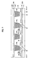
- FIG. 1 is an exploded perspective view illustrating a related art liquid crystal display device
- FIG. 2 is a plan view illustrating a related art liquid crystal display device including column spacers
- FIG. 3 is a cross-sectional configuration view taken along line I-I′ of FIG. 2 ;
- FIG. 4 is a cross-sectional view illustrating a liquid crystal display (LCD) device using protrusions
- FIGS. 5A and 5B are a cross-sectional view and a plan view, respectively, illustrating the relationship of a column spacer, protrusion, and recess in accordance with a first embodiment of the present invention
- FIG. 6 is a plan view illustrating a liquid crystal display device in accordance with a first embodiment of the present invention.
- FIG. 7 is a cross-sectional view taken along line II-II′ of FIG. 6 ;
- FIGS. 8A to 8C are cross-sectional views illustrating sequential processes of a method for manufacturing the liquid crystal display device in accordance with the first embodiment of the present invention.
- FIG. 9 is a plan view illustrating a liquid crystal display device in accordance with a second embodiment of the present invention.
- FIG. 4 is a cross-sectional view illustrating a liquid crystal display (LCD) device using protrusions.
- the LCD device of a type including an arrangement of protrusions includes first and second substrates 70 and 60 arranged to face each other, at least one column spacer 80 formed on the second substrate 60 at a predetermined position of the second substrate 60 , a protrusion 85 formed on the first substrate 70 that contacts a central portion of the upper surface of the column spacer 80 , the protrusion 85 having a top surface with a smaller area than that of an upper surface of the column spacer 80 , and a liquid crystal layer (not shown) filled between the first and second substrates 70 and 60 .
- the term “the upper surface” is named in relation to the second substrate 60 having the column spacer 80 such that the upper surface of the column spacer 80 is a surface facing the protrusion 85 and a lower surface of the column spacer 80 is a surface facing the second substrate 60 .
- the protrusion 85 which is interposed between the column spacer 80 and the first substrate 70 , has a top surface with a smaller area than that of the upper surface of the column spacer 80 , a contact area between the protrusion 85 and the column spacer 80 is small due to the smaller area of the top surface of the protrusion 85 .
- the column spacer 80 has a reduced frictional area with the protrusion 85 , resulting in a reduction in frictional force between the column spacer 80 and the protrusion 85 .
- an LCD device having the protrusion 85 in which the top surface has a smaller area than that of the upper surface of the column spacer 80 can eliminate the risk of a touch defect that occurs in LCD devices using column spacers 80 .
- the protrusion 85 which has a relatively small volume and a top surface with a small area, is initially positioned at the center of the column spacer 80 .
- the protrusion 85 has a problem in that, if an excessive pressure force is applied to the first or second substrate 70 or 60 , the force is concentrated on a center region of the upper surface of the column spacer 80 corresponding to the protrusion 85 , and the remaining region of the upper surface of the column spacer 80 not corresponding to the protrusion 85 can be brought into contact with the first substrate 70 facing the column spacer 80 .
- This disadvantageously increases contact area as compared to a configuration wherein only protrusion comes into contact with a substrate facing thereto, and therefore, results in an increased frictional force and a touch defect.
- embodiments according to the present invention capable of preventing the above described touch defect problem will be explained.
- FIGS. 5A and 5B are a cross-sectional view and a plan view, respectively, illustrating the relationship of a column spacer, protrusion, and recess in accordance with a first embodiment of the present invention.
- the LCD device with a recess includes first and second substrates 200 and 100 arranged to face each other, first and second uniformly spaced apart column spacers 50 a and 50 b arranged at predetermined positions on the second substrate 100 and having the same height as each other; a protrusion 51 formed on the first substrate 200 contacting a center portion of the first column spacer 50 a and having a top surface with a smaller area than an upper surface of the first column spacer 50 a (here, the upper surface being a surface corresponding to the protrusion 51 ), a recess 52 formed in the first substrate 200 to surround the protrusion 51 and have an outer periphery beyond the corresponding periphery of the upper surface of the first column spacer 50 a , and a liquid
- the recess 52 has an outer diameter (OD) W′ greater than the overall diameter of the corresponding upper surface of the first column spacer 50 a and an inner diameter (ID) W less than the overall diameter of the corresponding upper surface of the first column spacer 50 a .
- the outer and inner diameters W′ and W having a difference D.
- the inner diameter W is wider than the protrusion 51
- the outer diameter W′ is wider than a diameter of the upper surface of the first column spacer 50 a . Since the protrusion 51 is positioned to correspond to a center portion of the upper surface of the first column spacer 50 a , a periphery of the upper surface of the first column spacer 50 a is correspondingly within the recess 52 .
- the recess 52 may be formed via patterning of a gate insulation film 45 and passivation film 46 , which are stacked on a glass substrate 40 of the first substrate 200 in sequence, or by patterning of only the passivation film 46 .
- the second column spacer 50 b is spaced apart from the first substrate 200 by a predetermined gap due to the protrusion 51 coming into contact with the first column spacer 50 a.
- the first column spacer 50 a In embodiments of the present invention having the recess 52 , if an excessive pressure force is applied to a surface of the first or second substrate 200 or 100 , the first column spacer 50 a only contacts the protrusion 51 and does not come into contact with any other portion of the second substrate 200 . Therefore, a gap is maintained between the first substrate 200 and the second substrate 100 without an increase in contact area between elements of the first substrate 200 and the second substrate 100 . This has the effect of reducing the risk of a touch defect caused by an increased contact area between the upper surface of the first column spacer 50 a and an element other than the protrusion 51 of the first substrate 200 from coming into contact.
- FIG. 6 is a plan view illustrating an LCD device in accordance with a first embodiment of the present invention.
- FIG. 7 is a cross-sectional view taken along line II-II′ of FIG. 6 .
- the LCD device according to the first embodiment of the present invention which is operable in an IPS mode, includes first and second substrates 100 and 200 arranged to face each other, and a liquid crystal layer 55 between the first and second substrates 100 and 200 .
- the first substrate 100 which is a color filter substrate, includes a black matrix layer 31 formed on a first glass substrate 30 for blocking light through regions (corresponding to gate lines, data lines, and thin film transistors) other than pixel regions; a red R, green G, and blue B color filter layers (not shown) corresponding to the pixel regions for creating color tones; and an overcoat layer 33 formed over the entire surface of the first substrate 100 , including the black matrix layer 31 and color filter layers (not shown).
- a plurality of first and second column spacers 50 a and 50 b are formed on the overcoat layer 33 at predetermined positions of the overcoat layer 33 .
- the first and second column spacers 50 a and 50 b are made of photosensitive resin.
- the second substrate 200 which is a TFT substrate facing the color filter substrate 100 , includes a plurality of gate lines 41 and data lines 42 arranged on a second glass substrate 40 perpendicular to each other to define the pixel regions, common lines 47 arranged parallel to the gate lines 41 , uniformly spaced apart common electrodes 47 a protruding from the common lines 47 into the pixel regions, and pixel electrodes 43 extending parallel to the common electrodes 47 a between the common electrodes 47 a .
- the second substrate 200 also includes thin film transistors (TFTs) formed at crossings of the gate lines 41 and data lines 42 . Each of the TFTs have a source electrode 42 a connected to one of the data lines 42 , a gate electrode 41 a connected to one of the gate lines 41 , and a source electrode 42 b connected to one of the pixel electrodes 43 .
- TFTs thin film transistors
- a plurality of protrusions 51 are arranged on the gate lines 41 at positions corresponding to the first column spacers 50 a .
- the protrusions 51 are formed by depositing semiconductor layer 44 and a data line material. More specifically, each of the protrusions 51 has a laminated structure including a first protrusion pattern 44 a and a second protrusion pattern 42 c over the first protrusion pattern 44 a .
- the first protrusion pattern 44 a is formed by patterning the semiconductor layer 44 formed on the gate insulation film 45
- the second protrusion pattern 42 c is formed simultaneously when the source and drain electrodes 42 a and 42 b are formed at opposite sides of the respective patterned semiconductor layers 44 .
- a recess 52 is formed in the second substrate 200 to surround the protrusion 51 . That is, the recess 52 is configured to have an outer periphery beyond the corresponding periphery of the upper surface of the first column spacer 50 a and inner periphery within the corresponding periphery of the upper surface of the first column spacer 50 a .
- the recess 52 can be formed via patterning of the gate insulation film 45 and passivation film 46 , which are stacked on the second glass substrate 40 of the first substrate 200 in sequence, or via patterning of only the passivation film 46 .
- the manufacture of the TFT, pixel electrode, and recess begins by depositing a metal material, such as Mo, Al or Cr, over the second glass substrate 40 .
- a metal material such as Mo, Al or Cr
- the metal material is then patterned via a photolithography process to form the plurality of gate lines 41 , gate electrodes 41 a , common lines 47 , and common electrodes 47 a simultaneously. More specifically, the gate electrodes 41 a protrude from the gate lines 41 at predetermined positions in the pixel regions.
- an insulation material such as SiNx
- SiNx is deposited over the glass substrate 40 , including the gate lines 41 , gate electrodes 41 a , common lines 47 , and common electrodes 47 a , to form the gate insulation film 45 .
- a semiconductor layer is deposited on the gate insulation film 45 .
- the deposited semiconductor layer is then patterned to form the semiconductor layers 44 on the gate insulation film 45 over the gate electrodes 41 a .
- the first protrusion patterns 44 a of the protrusions 51 are formed on the gate insulation film 45 at positions corresponding to the first column spacers 50 a , respectively.
- the semiconductor layers 44 are formed by sequentially depositing an amorphous silicon layer or a poly-silicon layer and a silicon layer doped with an impurity, and subsequently, patterning both the amorphous silicon layer(or poly-silicon layer) and doped silicon layer at the same time.
- a metal material such as Mo, Al or Cr, is then deposited and patterned via a photolithography process to form the plurality of data lines 42 perpendicular to the gate lines 41 .
- the source and drain electrodes 42 a and 42 b are formed to be in contact with opposite sides of the respective semiconductor layers 44 , and simultaneously, the second protrusion patterns 42 c are formed on the first protrusion patterns 44 a , respectively.
- the plurality of protrusions 51 are formed of the first protrusion patterns 44 a and second protrusion patterns 42 c .
- the source electrodes 42 a protrude from the data lines 42 a.
- the passivation film 46 is deposited over the entire surface of the second substrate 200 , including the source and drain electrodes 42 a and 42 b .
- the passivation film can be made of an inorganic material, such as SiNx, an organic material having a low dielectric constant, such as BenzoCycloButene (BCB), Spin On Glass (SOG), or Acryl, can instead be used to improve the aperture ratio of liquid crystal cells.
- Predetermined regions of the passivation film 46 over the drain electrodes 42 b are then selectively etched to form drain contact holes (designated as reference numeral 54 in FIG. 8B ) exposing a part of the respective drain electrodes 42 b to the outside.
- the recesses 52 are formed by removing certain regions of the passivation film 46 and gate insulation film 45 such that the periphery of the upper surface of each of the first column spacers 50 a is directly above a corresponding recess 52 .
- FIGS. 8A to 8C are cross-sectional views illustrating sequential processes of a method for manufacturing the liquid crystal display device in accordance with the first embodiment of the present invention. The formation of the drain contact holes and recesses will be explained with reference to FIGS. 8A and 8B .
- FIG. 8A is a cross-sectional view taken along line IV-IV′ of FIG. 6
- FIG. 8A is a cross-sectional view taken along the line III-III′ of FIG. 6 .
- the photoresist is subjected to exposure and development processes, to form photoresist patterns PR for use in the formation of the drain contact holes and recesses.
- the passivation film 46 is patterned by using the photoresist patterns PR as a mask, to form the drain contact holes 54 exposing the drain electrodes 42 b to the outside.
- both the passivation film 46 and gate insulation film 45 are patterned by using the photoresist patterns PR as a mask, to form the recesses 52 .
- the remaining photoresist patterns PR are completely removed. In this way, the recesses 52 are formed to correspond to the peripheral regions of the upper surfaces of the respective first column spacers 50 a.
- a transparent conductive film 56 is deposited over the passivation film 46 , so as to be electrically connected to the drain electrodes 42 b through the drain contact holes 54 .
- the deposited transparent conductive film 56 is then selectively removed, to form the pixel electrodes 43 in the respective pixel regions.
- the pixel electrodes are formed such that they are connected to the drain electrodes 42 b while extending parallel to the common electrodes 47 a between the common electrodes 47 a.
- the transparent conductive film 56 which is deposited for forming the pixel electrodes 43 , can also be deposited over the recesses 52 and the passivation film 56 on the protrusion 51 .
- the transparent conductive film 56 serves as a protective film for the gate electrodes 41 a exposed in the recesses 52 .
- processes for forming orientation films over the color filter array substrate 100 having the first and second column spacers 50 a and 50 b and over the TFT array substrate 200 having the recesses 52 , respectively, may be included in the TFT array process and color filter array process.
- the column spacers are formed on the color filter substrate and the recesses are formed on the TFT substrate, embodiments of the present invention are not limited thereto, and it should be understood that the column spacers may be formed on the TFT substrate and the recesses may be formed on the color filter substrate.
- the first embodiment of the present invention illustrates the IPS mode LCD device, the present invention is not limited thereto, but may be applied to a TN mode LCD device.
- FIG. 9 is a plan view illustrating a TN mode LCD device in accordance with a second embodiment of the present invention.
- the cross-sectional view taken along line V-V′ of FIG. 9 would be the same as the cross-sectional view taken along the same area of the IPS mode LCD device in accordance with the first embodiment of the present invention, and therefore, a detailed configuration thereof refers to FIG. 7 .
- the structure of the TN mode LCD device will be explained in detail.
- the first color filter substrate 100 includes the black matrix layer 31 formed on the first glass substrate 30 for blocking light through regions corresponding to gate lines, data lines, and thin film transistors; the red, green, and blue color filter layers (not shown) corresponding to the pixel regions for creating color tones; and a common electrode (not shown) formed over the entire surface of the first substrate 100 , including the black matrix layer 31 and color filter layer (not shown).
- the plurality of first and second column spacers 50 a and 50 b are formed on the common electrode (not shown) at predetermined positions on the common electrode.
- the first and second column spacers 50 a and 50 b are made of photosensitive resin.
- the second TFT substrate 200 facing the color filter substrate 100 includes: a plurality of gate lines 41 and data lines 42 arranged on the second glass substrate 40 perpendicular to each other to define the pixel regions; the pixel electrodes 43 formed at the respective pixel regions; and the TFTs formed at crossings of the gate lines 41 and data lines 42 .
- the plurality of protrusions 51 are arranged on the gate lines 41 at positions corresponding to the first column spacers 50 a .
- the protrusions 51 are formed via deposition of the semiconductor layer 44 and data line material.
- Each of the protrusions 51 has a laminated structure including the first protrusion pattern 44 a and second protrusion pattern 42 c over the first protrusion pattern 44 a .
- the first protrusion pattern 44 a is formed via patterning of the semiconductor layer 44 on the gate insulation film 45 .
- the second protrusion pattern 42 c is formed simultaneously when the source and drain electrodes 42 a and 42 b are formed at opposite sides of the patterned semiconductor layers 44 .
- Each protrusion 51 contacts a center portion of the upper surface of the associated first column spacers 50 a .
- a recess 52 is formed in the second substrate 200 surrounding the protrusion 51 and having an outer periphery beyond the corresponding periphery of the upper surface of the first column spacer 50 a.
- the recesses 52 are formed by patterning certain portions of the gate insulation film 45 and passivation film 46 , which are stacked on the glass substrate 40 of the second substrate 200 in sequence. Alternatively, the recesses 52 may be formed by patterning predetermined portions of only the passivation film 46 .
- the manufacture of the TFT, pixel electrode, and recess begins by depositing a metal material, such as Mo, Al or Cr, over the second glass substrate 40 .
- a metal material such as Mo, Al or Cr
- the metal material is then patterned via a photolithography process to form the plurality of gate lines 41 , gate electrodes 41 a , common lines 47 , and common electrodes 47 a simultaneously. More specifically, the gate electrodes 41 a protrude from the gate lines 41 at predetermined positions in the pixel regions.
- an insulation material such as SiNx
- SiNx is deposited over the glass substrate 40 having the gate lines 41 and gate electrodes 41 a , to form the gate insulation film 45 .
- a semiconductor layer is deposited on the gate insulation film 45 .
- the deposited semiconductor layer is then patterned, to form the semiconductor layers 44 on the gate insulation film 45 over the gate electrodes 41 a .
- the semiconductor layer 44 is formed by sequentially depositing an amorphous silicon layer or poly-silicon layer and a silicon layer doped with a high density impurity, and subsequently, patterning both the amorphous silicon layer(or poly-silicon layer) and doped silicon layer simultaneously.
- a metal material such as Mo, Al or Cr, is deposited, the metal material is patterned by use of a photolithography process, to form the plurality of data lines 42 perpendicular to the gate lines 41 .
- the source and drain electrodes 42 a and 42 b are formed contacting opposite sides of the semiconductor layers 44 , respectively.
- the source electrodes 42 a protrude from the data lines 42 a.
- the second protrusion pattern 42 c is formed on the first protrusion pattern 44 a .
- the plurality of protrusions 51 are formed of the first protrusion pattern 44 a and second protrusion pattern 42 c.
- the passivation film 46 is deposited over the entire surface of the second substrate 200 , including the source and drain electrodes 42 a and 42 b .
- the passivation film can be made of an inorganic material, such as SiNx, an organic material having a low dielectric constant, such as BenzoCycloButene (BCB), Spin On Glass (SOG), or Acryl, can be used to improve the aperture ratio of liquid crystal cells.
- BCB BenzoCycloButene
- SOG Spin On Glass
- Acryl Acryl
- the recesses 52 are formed by removing certain regions of the passivation film 46 and gate insulation film 45 corresponding to the outer periphery of the upper surface of the respective first column spacers 50 a .
- the formation of the recesses is accomplished in the same manner as that of the IPS mode LCD device according to the first embodiment of the present invention as shown in FIGS. 8A and 8B , and thus, no detailed description thereof will be given.
- a transparent conductive film is deposited over the passivation film 46 , so as to be electrically connected to the drain electrodes 42 b through the drain contact holes 54 .
- the deposited transparent conductive film 56 is then selectively removed, to form the pixel electrodes 43 at the respective pixel regions.
- the transparent conductive film 56 which is deposited for forming the pixel electrodes 43 , can also deposited over the recesses 52 and the passivation film 56 on the protrusion 51 to serve as a protective film for the gate electrodes 41 a at the bottom of the recesses 52 .
- processes for forming orientation films over the color filter array substrate 100 having the first and second column spacers 50 a and 50 b and over the TFT array substrate 200 having the recesses 52 , respectively, may be included in the TFT array process and color filter array process.
- the column spacers are formed at the color filter substrate and the recesses are formed at the TFT substrate, embodiments of the present invention are not limited thereto, and it should be understood that the column spacers may be formed on the TFT substrate and the recesses may be formed on the color filter substrate.
Abstract
Description
Claims (11)
Priority Applications (1)
| Application Number | Priority Date | Filing Date | Title |
|---|---|---|---|
| US12/314,696 US7684003B2 (en) | 2005-12-15 | 2008-12-15 | Liquid crystal display device and method for manufacturing the same |
Applications Claiming Priority (2)
| Application Number | Priority Date | Filing Date | Title |
|---|---|---|---|
| KR10-2005-0123660 | 2005-12-15 | ||
| KR1020050123660A KR101192783B1 (en) | 2005-12-15 | 2005-12-15 | Liquid Crystal Display Device and Method of manufacturing the same |
Related Child Applications (1)
| Application Number | Title | Priority Date | Filing Date |
|---|---|---|---|
| US12/314,696 Division US7684003B2 (en) | 2005-12-15 | 2008-12-15 | Liquid crystal display device and method for manufacturing the same |
Publications (2)
| Publication Number | Publication Date |
|---|---|
| US20070139604A1 US20070139604A1 (en) | 2007-06-21 |
| US7483113B2 true US7483113B2 (en) | 2009-01-27 |
Family
ID=38165623
Family Applications (2)
| Application Number | Title | Priority Date | Filing Date |
|---|---|---|---|
| US11/475,214 Active 2027-04-28 US7483113B2 (en) | 2005-12-15 | 2006-06-27 | Liquid crystal display device and method for manufacturing the same |
| US12/314,696 Active US7684003B2 (en) | 2005-12-15 | 2008-12-15 | Liquid crystal display device and method for manufacturing the same |
Family Applications After (1)
| Application Number | Title | Priority Date | Filing Date |
|---|---|---|---|
| US12/314,696 Active US7684003B2 (en) | 2005-12-15 | 2008-12-15 | Liquid crystal display device and method for manufacturing the same |
Country Status (5)
| Country | Link |
|---|---|
| US (2) | US7483113B2 (en) |
| JP (1) | JP4566165B2 (en) |
| KR (1) | KR101192783B1 (en) |
| CN (1) | CN100456096C (en) |
| TW (1) | TWI350936B (en) |
Cited By (4)
| Publication number | Priority date | Publication date | Assignee | Title |
|---|---|---|---|---|
| US20100053536A1 (en) * | 2008-08-26 | 2010-03-04 | Hitachi Displays, Ltd. | Liquid crystal display device |
| US20120113343A1 (en) * | 2010-11-09 | 2012-05-10 | Nlt Technologies, Ltd. | Liquid crystal display device |
| US20140198284A1 (en) * | 2013-01-11 | 2014-07-17 | Hannstar Display Corporation | Liquid crystal display panel |
| US10315417B2 (en) | 2015-02-13 | 2019-06-11 | Hewlett-Packard Development Company, L.P. | Printhead employing data packets including address data |
Families Citing this family (40)
| Publication number | Priority date | Publication date | Assignee | Title |
|---|---|---|---|---|
| KR101137842B1 (en) * | 2005-09-23 | 2012-04-20 | 엘지디스플레이 주식회사 | Liquid Crystal Display Device and Method for Manufacturing the Same |
| KR101157954B1 (en) * | 2005-09-28 | 2012-06-22 | 엘지디스플레이 주식회사 | Liquid Crystal Display Device and Method for Manufacturing the Same |
| US8319302B2 (en) * | 2007-06-22 | 2012-11-27 | Agency For Science, Technology And Research | Wafer arrangement and a method for manufacturing the wafer arrangement |
| CN101334562A (en) * | 2007-06-29 | 2008-12-31 | 群康科技(深圳)有限公司 | Liquid crystal display panel |
| JP5323329B2 (en) * | 2007-08-10 | 2013-10-23 | パナソニック液晶ディスプレイ株式会社 | Liquid crystal display |
| TWI329221B (en) * | 2007-09-04 | 2010-08-21 | Au Optronics Corp | Touch panel |
| KR100997979B1 (en) * | 2008-04-30 | 2010-12-02 | 삼성전자주식회사 | Liquid crystal display and method for manufacturing the same |
| KR101490473B1 (en) | 2008-07-01 | 2015-02-06 | 삼성디스플레이 주식회사 | Liquid crystal display including color filters |
| JP4600547B2 (en) * | 2008-08-27 | 2010-12-15 | ソニー株式会社 | Liquid crystal display |
| JP2010096993A (en) * | 2008-10-16 | 2010-04-30 | Sony Corp | Liquid crystal display device and method of manufacturing same |
| JP4716056B2 (en) * | 2008-12-19 | 2011-07-06 | ソニー株式会社 | Liquid crystal display device and electronic device |
| JP2010237503A (en) * | 2009-03-31 | 2010-10-21 | Hitachi Displays Ltd | Liquid crystal display |
| JP5500013B2 (en) * | 2010-09-08 | 2014-05-21 | カシオ計算機株式会社 | Touch-type liquid crystal display device with built-in contacts |
| KR101731398B1 (en) * | 2010-10-28 | 2017-05-02 | 삼성디스플레이 주식회사 | Liquid crystal display and method for manufacturing the same |
| JP5285729B2 (en) | 2011-03-03 | 2013-09-11 | 株式会社ジャパンディスプレイ | Liquid crystal display |
| WO2012147592A1 (en) * | 2011-04-25 | 2012-11-01 | シャープ株式会社 | Liquid crystal display panel and liquid crystal display device |
| CN102243397A (en) | 2011-07-05 | 2011-11-16 | 深圳市华星光电技术有限公司 | Liquid crystal panel and spacer structure thereof |
| CN102243398A (en) * | 2011-07-06 | 2011-11-16 | 深圳市华星光电技术有限公司 | Liquid crystal display device |
| CN102243400A (en) * | 2011-07-12 | 2011-11-16 | 南京中电熊猫液晶显示科技有限公司 | Liquid crystal display |
| KR101820661B1 (en) | 2011-07-19 | 2018-01-23 | 엘지디스플레이 주식회사 | Liquid crystal display device |
| CN102654948B (en) * | 2011-08-30 | 2014-04-16 | 京东方科技集团股份有限公司 | Display panel for blind and manufacturing method of display panel, blind display device |
| KR101910340B1 (en) | 2011-10-12 | 2018-10-23 | 삼성디스플레이 주식회사 | Liquid crystal display having narrow bezel |
| KR101396943B1 (en) * | 2012-06-25 | 2014-05-19 | 엘지디스플레이 주식회사 | Liquid crystal display device and method for fabricating the same |
| JP2014032332A (en) * | 2012-08-03 | 2014-02-20 | Japan Display Inc | Liquid crystal display device |
| CN102967971B (en) * | 2012-11-02 | 2015-09-23 | 京东方科技集团股份有限公司 | Array base palte and display device |
| JP2013054391A (en) * | 2012-12-18 | 2013-03-21 | Japan Display East Co Ltd | Liquid crystal display device |
| CN103901670B (en) * | 2012-12-28 | 2017-09-15 | 群康科技(深圳)有限公司 | Display device |
| KR20150040648A (en) | 2013-10-07 | 2015-04-15 | 삼성디스플레이 주식회사 | LIQUID CRYSTAL DISPlAY |
| KR102178488B1 (en) * | 2014-03-06 | 2020-11-16 | 엘지디스플레이 주식회사 | Liquid Crystal Display Device |
| CN104020601A (en) * | 2014-05-29 | 2014-09-03 | 深圳市华星光电技术有限公司 | Color film substrate and display device |
| TWI596780B (en) * | 2014-10-27 | 2017-08-21 | 友達光電股份有限公司 | Array substrate |
| CN104330924A (en) * | 2014-11-25 | 2015-02-04 | 重庆京东方光电科技有限公司 | Display substrate, display panel, display device and method for forming spacer |
| CN104656305A (en) * | 2015-03-09 | 2015-05-27 | 京东方科技集团股份有限公司 | Color film display layer, display panel and preparation method thereof |
| CN104793407A (en) * | 2015-04-29 | 2015-07-22 | 深圳市华星光电技术有限公司 | Liquid crystal display panel and liquid crystal display |
| CN104900709B (en) * | 2015-06-04 | 2017-11-17 | 福州大学 | A kind of high-performance bottom gate type TFT device architectures and preparation method thereof |
| TWI542925B (en) * | 2015-06-16 | 2016-07-21 | 凌巨科技股份有限公司 | Display panel |
| KR102360821B1 (en) * | 2015-06-26 | 2022-02-09 | 엘지디스플레이 주식회사 | Display device |
| TWI548911B (en) * | 2015-08-26 | 2016-09-11 | 友達光電股份有限公司 | Display panel |
| KR102631187B1 (en) * | 2016-10-31 | 2024-01-29 | 엘지디스플레이 주식회사 | Liquid Crystal Display Device |
| CN111176023A (en) * | 2018-11-12 | 2020-05-19 | 惠科股份有限公司 | Display panel and display device with increased segment difference |
Citations (6)
| Publication number | Priority date | Publication date | Assignee | Title |
|---|---|---|---|---|
| US6690441B2 (en) * | 2000-09-22 | 2004-02-10 | Dai Nippon Printing Co., Ltd. | Multi-domain vertical alignment mode liquid crystal display having spacers formed over zigzag like alignment-controlling projection |
| JP2005107452A (en) | 2003-10-02 | 2005-04-21 | Sony Corp | Method for manufacturing liquid crystal display element, liquid crystal display element, projection display apparatus and method for laminating substrate |
| US20050185129A1 (en) * | 2004-02-25 | 2005-08-25 | Lg.Philips Lcd Co., Ltd. | Liquid crystal display device and method of fabricating the same |
| CN1693977A (en) | 2004-04-30 | 2005-11-09 | Lg.菲利浦Lcd株式会社 | Liquid crystal display device and method for fabricating the same |
| US20070115420A1 (en) * | 2005-11-21 | 2007-05-24 | Chunghwa Picture Tubes, Ltd. | Liquid crystal display device |
| US20070216847A1 (en) * | 2006-03-15 | 2007-09-20 | Tsung-Chien Chang | Liquid crystal display panel |
Family Cites Families (6)
| Publication number | Priority date | Publication date | Assignee | Title |
|---|---|---|---|---|
| US6738125B2 (en) * | 1999-12-27 | 2004-05-18 | Sharp Kabushiki Kaisha | Liquid crystal display apparatus and method for manufacturing same |
| US7292304B2 (en) * | 2001-12-17 | 2007-11-06 | Lg.Philips Lcd Co., Ltd. | Liquid crystal display panel and method for fabricating the same comprising a dummy column spacer to regulate a liquid crystal flow and a supplemental dummy column spacer formed substantially parallel and along the dummy column spacer |
| TWI358830B (en) * | 2003-12-12 | 2012-02-21 | Samsung Electronics Co Ltd | Array substrate, method of manufacturing the same |
| TWI257500B (en) * | 2004-01-16 | 2006-07-01 | Hannstar Display Corp | Liquid crystal display substrate, manufacturing method thereof and liquid crystal display containing the substrate |
| US7561245B2 (en) * | 2004-02-25 | 2009-07-14 | Lg Display Co., Ltd. | Liquid crystal display device and method of fabricating the same |
| KR100641002B1 (en) * | 2004-04-30 | 2006-11-02 | 엘지.필립스 엘시디 주식회사 | Liquid Crystal Display Device |
-
2005
- 2005-12-15 KR KR1020050123660A patent/KR101192783B1/en active IP Right Grant
-
2006
- 2006-06-27 US US11/475,214 patent/US7483113B2/en active Active
- 2006-06-28 TW TW095123424A patent/TWI350936B/en active
- 2006-06-29 CN CNB2006100904995A patent/CN100456096C/en active Active
- 2006-06-30 JP JP2006180801A patent/JP4566165B2/en active Active
-
2008
- 2008-12-15 US US12/314,696 patent/US7684003B2/en active Active
Patent Citations (7)
| Publication number | Priority date | Publication date | Assignee | Title |
|---|---|---|---|---|
| US6690441B2 (en) * | 2000-09-22 | 2004-02-10 | Dai Nippon Printing Co., Ltd. | Multi-domain vertical alignment mode liquid crystal display having spacers formed over zigzag like alignment-controlling projection |
| JP2005107452A (en) | 2003-10-02 | 2005-04-21 | Sony Corp | Method for manufacturing liquid crystal display element, liquid crystal display element, projection display apparatus and method for laminating substrate |
| US20050185129A1 (en) * | 2004-02-25 | 2005-08-25 | Lg.Philips Lcd Co., Ltd. | Liquid crystal display device and method of fabricating the same |
| CN1661424A (en) | 2004-02-25 | 2005-08-31 | Lg.菲利浦Lcd株式会社 | Liquid crystal display device and method of fabricating the same |
| CN1693977A (en) | 2004-04-30 | 2005-11-09 | Lg.菲利浦Lcd株式会社 | Liquid crystal display device and method for fabricating the same |
| US20070115420A1 (en) * | 2005-11-21 | 2007-05-24 | Chunghwa Picture Tubes, Ltd. | Liquid crystal display device |
| US20070216847A1 (en) * | 2006-03-15 | 2007-09-20 | Tsung-Chien Chang | Liquid crystal display panel |
Cited By (5)
| Publication number | Priority date | Publication date | Assignee | Title |
|---|---|---|---|---|
| US20100053536A1 (en) * | 2008-08-26 | 2010-03-04 | Hitachi Displays, Ltd. | Liquid crystal display device |
| US20120113343A1 (en) * | 2010-11-09 | 2012-05-10 | Nlt Technologies, Ltd. | Liquid crystal display device |
| US8659732B2 (en) * | 2010-11-09 | 2014-02-25 | Nlt Technologies, Ltd. | Liquid crystal display device |
| US20140198284A1 (en) * | 2013-01-11 | 2014-07-17 | Hannstar Display Corporation | Liquid crystal display panel |
| US10315417B2 (en) | 2015-02-13 | 2019-06-11 | Hewlett-Packard Development Company, L.P. | Printhead employing data packets including address data |
Also Published As
| Publication number | Publication date |
|---|---|
| US7684003B2 (en) | 2010-03-23 |
| CN1982967A (en) | 2007-06-20 |
| TWI350936B (en) | 2011-10-21 |
| JP4566165B2 (en) | 2010-10-20 |
| TW200722875A (en) | 2007-06-16 |
| US20090104725A1 (en) | 2009-04-23 |
| JP2007164134A (en) | 2007-06-28 |
| CN100456096C (en) | 2009-01-28 |
| KR101192783B1 (en) | 2012-10-18 |
| US20070139604A1 (en) | 2007-06-21 |
| KR20070063662A (en) | 2007-06-20 |
Similar Documents
| Publication | Publication Date | Title |
|---|---|---|
| US7483113B2 (en) | Liquid crystal display device and method for manufacturing the same | |
| KR101413275B1 (en) | Liquid crystal display panel and method of manufacturing the same | |
| US9281320B2 (en) | Array substrate and liquid crystal display apparatus having the same | |
| JP4925030B2 (en) | Liquid crystal display device and manufacturing method thereof | |
| US8199271B2 (en) | Liquid crystal display device with active layer over the gate line, data line, gate electrode and source/drain electrodes | |
| US7859629B2 (en) | In-plane switching mode liquid crystal display wherein the upper and lower pixel electrodes are arranged on opposite sides of the respective upper and lower pixel regions | |
| US8243218B2 (en) | Liquid crystal display device and method for manufacturing the same | |
| US7417705B2 (en) | Liquid crystal display device and method for fabricating the same | |
| US20080001883A1 (en) | Liquid Crystal Display Device and Method for Fabricating the Same | |
| KR101430610B1 (en) | Liquid crystal display panel and method for manufacturing the same. | |
| US8514360B2 (en) | LCD device | |
| KR101980773B1 (en) | Thin film transistor substrate having color filter and method of fabricating the same | |
| US7724325B2 (en) | Liquid crystal display device and method for manufacturing the same | |
| US7385661B2 (en) | In-plane switching mode liquid crystal display device and method of manufacturing the same | |
| US20080291384A1 (en) | Display apparatus and method of manufacturing the same | |
| KR101362960B1 (en) | Liquid crystal display device and fabricating method thereof | |
| US7847889B2 (en) | Panel for display device with light blocking on blue color filter and liquid crystal display | |
| KR20130049108A (en) | Liquid crystal display device having multi column spacer | |
| KR100510188B1 (en) | Liquid Crystal Display Panel and Method of Fabricating the same | |
| KR20080078993A (en) | Liquid crystal display device and method for manufacturing of the same | |
| KR101266573B1 (en) | Liquid Crystal Display Pannel and Method of Fabricating the same | |
| KR20080062121A (en) | Liquid crystal display panel and method for fabricating thereof |
Legal Events
| Date | Code | Title | Description |
|---|---|---|---|
| AS | Assignment |
Owner name: LG.PHILIPS LCD CO., LTD., KOREA, REPUBLIC OF Free format text: ASSIGNMENT OF ASSIGNORS INTEREST;ASSIGNORS:PAIK, SANG Y.;LEE, JOON Y.;REEL/FRAME:018032/0640 Effective date: 20060614 |
|
| AS | Assignment |
Owner name: LG DISPLAY CO., LTD., KOREA, REPUBLIC OF Free format text: CHANGE OF NAME;ASSIGNOR:LG.PHILIPS LCD CO., LTD.;REEL/FRAME:021772/0701 Effective date: 20080304 Owner name: LG DISPLAY CO., LTD.,KOREA, REPUBLIC OF Free format text: CHANGE OF NAME;ASSIGNOR:LG.PHILIPS LCD CO., LTD.;REEL/FRAME:021772/0701 Effective date: 20080304 |
|
| FEPP | Fee payment procedure |
Free format text: PAYOR NUMBER ASSIGNED (ORIGINAL EVENT CODE: ASPN); ENTITY STATUS OF PATENT OWNER: LARGE ENTITY |
|
| STCF | Information on status: patent grant |
Free format text: PATENTED CASE |
|
| FEPP | Fee payment procedure |
Free format text: PAYER NUMBER DE-ASSIGNED (ORIGINAL EVENT CODE: RMPN); ENTITY STATUS OF PATENT OWNER: LARGE ENTITY Free format text: PAYOR NUMBER ASSIGNED (ORIGINAL EVENT CODE: ASPN); ENTITY STATUS OF PATENT OWNER: LARGE ENTITY |
|
| FPAY | Fee payment |
Year of fee payment: 4 |
|
| FPAY | Fee payment |
Year of fee payment: 8 |
|
| MAFP | Maintenance fee payment |
Free format text: PAYMENT OF MAINTENANCE FEE, 12TH YEAR, LARGE ENTITY (ORIGINAL EVENT CODE: M1553); ENTITY STATUS OF PATENT OWNER: LARGE ENTITY Year of fee payment: 12 |