US7398075B2 - Radio wave reception device and radio wave clock - Google Patents
Radio wave reception device and radio wave clock Download PDFInfo
- Publication number
- US7398075B2 US7398075B2 US10/521,618 US52161805A US7398075B2 US 7398075 B2 US7398075 B2 US 7398075B2 US 52161805 A US52161805 A US 52161805A US 7398075 B2 US7398075 B2 US 7398075B2
- Authority
- US
- United States
- Prior art keywords
- frequency
- signal
- radio wave
- circuit
- khz
- Prior art date
- Legal status (The legal status is an assumption and is not a legal conclusion. Google has not performed a legal analysis and makes no representation as to the accuracy of the status listed.)
- Expired - Lifetime, expires
Links
- 230000010355 oscillation Effects 0.000 claims abstract description 143
- 238000006243 chemical reaction Methods 0.000 claims description 72
- 238000001514 detection method Methods 0.000 claims description 61
- 238000000034 method Methods 0.000 description 32
- 230000001360 synchronised effect Effects 0.000 description 24
- 238000010586 diagram Methods 0.000 description 18
- 230000006870 function Effects 0.000 description 15
- 230000002194 synthesizing effect Effects 0.000 description 8
- 230000015572 biosynthetic process Effects 0.000 description 4
- 230000008859 change Effects 0.000 description 4
- 230000010363 phase shift Effects 0.000 description 4
- 238000003786 synthesis reaction Methods 0.000 description 4
- 230000005540 biological transmission Effects 0.000 description 3
- 230000008901 benefit Effects 0.000 description 2
- 238000012937 correction Methods 0.000 description 2
- 238000012545 processing Methods 0.000 description 2
- 238000001228 spectrum Methods 0.000 description 2
- 238000001914 filtration Methods 0.000 description 1
- 239000004973 liquid crystal related substance Substances 0.000 description 1
- 238000012986 modification Methods 0.000 description 1
- 230000004048 modification Effects 0.000 description 1
- 230000004044 response Effects 0.000 description 1
- 238000012546 transfer Methods 0.000 description 1
Images



Classifications
-
- G—PHYSICS
- G04—HOROLOGY
- G04R—RADIO-CONTROLLED TIME-PIECES
- G04R20/00—Setting the time according to the time information carried or implied by the radio signal
- G04R20/08—Setting the time according to the time information carried or implied by the radio signal the radio signal being broadcast from a long-wave call sign, e.g. DCF77, JJY40, JJY60, MSF60 or WWVB
- G04R20/10—Tuning or receiving; Circuits therefor
Definitions
- the present invention relates to a radio wave reception device and a radio wave clock.
- low-frequency standard radio waves containing time data (that is, a time code) are transmitted in various countries (for example, Germany, the United Kingdom, Switzerland, Japan, and so forth).
- a time code for example, 40-kHz and 60-kHz low-frequency standard radio waves that have been subjected to amplitude modulation using a time code having a format shown in FIG. 12 , are transmitted from two transmission facilities located in Fukushima Prefecture and Saga Prefecture).
- the time code comprises a plurality of frame is defined to have a time cycle of 60 seconds.
- the time code is transmitted in a frame every time the figure representing the minute of an accurate time is updated (that is every minute).
- radio wave clocks that receive such time codes and correct time data of a timekeeping circuit based on the received time codes have been put into practical use.
- radio wave clocks which are adjusted to a so-called multi-band to become able to receive radio waves of both the frequencies (40 kHz and 60 kHz).
- radio wave clocks are equipped inside with a straight receiving circuit adjusted to each frequency.
- An object of the present invention is to provide a radio wave reception device and a radio wave clock which are capable of multi-frequency reception, which do not require complicated structures for receiving circuits and thus have simple structures, and which can save the amount of power consumption.
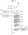
- FIG. 1 is a block diagram showing an internal structure of a radio wave clock
- FIG. 2 is a block diagram showing a circuit structure of a radio wave reception device according to a first embodiment
- FIG. 3 is a flowchart showing a frequency switching operation
- FIG. 4 is a block diagram showing a circuit structure of a radio wave reception device according to a second embodiment
- FIG. 5 is a block diagram showing a circuit structure of a radio wave reception device according to a third embodiment
- FIG. 6 is a block diagram showing a circuit structure of a radio wave reception device according to a fourth embodiment
- FIG. 7 is a flowchart showing a switching operation according to the fourth embodiment.
- FIG. 8 is a modified example of the block diagram showing the circuit structure of the radio wave reception device according to the fourth embodiment.
- FIG. 9 is a block diagram showing a circuit structure of a radio wave reception device according to a fifth embodiment.
- FIG. 10 is a flowchart showing a switching operation according to the fifth embodiment.
- FIG. 11 is a modified example of the block diagram showing the circuit structure of the radio wave reception device according to the fifth embodiment.
- FIG. 12 is a diagram showing a time code of a low-frequency standard radio wave.
- FIG. 1 is a diagram showing a circuit structure of a radio wave clock 900 .
- the radio wave clock 900 comprises a CPU (Central Processing Unit) 901 , an input unit 902 , a display unit 903 , a RAM (Random Access Memory) 905 , a ROM (Read Only Memory) 906 , a reception control unit 907 , a timekeeping circuit 908 , and a time code conversion unit 910 .
- the respective units are connected by a bus 913 .
- an oscillation circuit 909 is connected to the timekeeping circuit 908 .
- the CPU 901 reads out various programs stored in the ROM 906 at a predetermined timing or in accordance with an operation signal and the like input from the input unit 902 , and expands the read-out programs in the RAM 905 in order to give instructions or transfer data to each functional unit based on the programs.
- the CPU 901 controls the reception control unit 907 at every predetermined interval to perform an operation for receiving a standard radio wave. Then, the CPU 901 corrects data representing a current time which is kept by the timekeeping circuit 908 based on a standard time code input by the reception control unit 907 , and outputs a display signal generated based on the corrected current time data to the display unit 903 to make the displayed time updated.
- the CPU 901 determines whether or not a standard radio wave has been received, and performs various operations such as outputting a signal for controlling to switch frequencies of a signal to be selected to the reception control unit 907 . Furthermore, the CPU 901 has a function as selection means.
- the input unit 902 comprises switches for controlling the radio wave clock 900 to perform various functions. When any of these switches is operated, an operation signal corresponding to the operated switch is output to the CPU 901 .
- the display unit 903 is constituted by a compact liquid crystal display or the like, and digitally displays data from the CPU 901 , for example, the current time data of the timekeeping circuit 908 .
- the RAM 905 stores data processed by the CPU 901 and outputs stored data to the CPU 901 under the control of the CPU 901 .
- the ROM 906 mainly stores system programs and application programs pertinent to the radio wave clock 900 . Further, according to the present embodiment, the ROM 906 stores a frequency switching program 916 .
- the frequency-switching program 916 is a program for controlling a frequency selection circuit 2 included in a later-described radio wave reception device 917 to switch frequencies to be selected.
- the reception control unit 907 comprises the radio wave reception device 917 .
- the radio wave reception device 917 cuts off unnecessary frequency components from a standard radio wave received by an antenna to pick out a targeted frequency signal, and outputs an electric signal converted from the frequency signal to the time code conversion unit 910 .
- the timekeeping circuit 908 counts signals input from the oscillation circuit 909 , and obtains the current time data and the like. Then, the timekeeping circuit 908 outputs the obtained current time data to the CPU 901 .
- the oscillation circuit 909 is a circuit that outputs a signal having a constant frequency all the time.
- the time code conversion unit 910 generates a standard time code including data necessary for the function as a clock, such as a standard time code, a count-up code, a day code, etc. based on the signal output from the radio wave reception device 917 , and outputs the generated standard time code to the CPU 901 .
- FIG. 2 is a block diagram showing a circuit structure of the radio wave reception device 917 employing a super heterodyne method according to the present embodiment.
- the radio wave reception device 917 comprises an antenna 1 , a frequency selection circuit 2 , a high frequency amplifier circuit 3 , a frequency conversion circuit 4 , a local oscillation circuit 5 , a filter circuit 6 , an intermediate frequency amplifier circuit 7 , and a detection circuit 8 .
- the antenna 1 can receive two kinds of radio waves whose frequencies are either f 1 or f 2 (for example, 40 kHz or 60 kHz).
- the antenna 1 is constituted by, for example, a bar antenna A received radio wave is converted into an electric signal and then output.
- the frequency selection circuit 2 receives signals output from the antenna 1 , and selects and outputs a signal whose frequency is f 1 or f 2 . In the present embodiment, it is initially set that a signal having frequency of f 1 should be selected. The frequency selection circuit 2 switches frequencies to be selected to f 1 or f 2 in accordance with a signal S 1 input from the detection circuit 8 or a signal S 2 input from the CPU 901 .
- the high frequency amplifier circuit 3 amplifies and outputs the signal input from the frequency selection circuit 2 .
- the antenna 1 and the frequency selection circuit 2 have a function as radio wave reception means.
- the frequency conversion circuit 4 synthesizes the signal input from the high frequency amplifier circuit 3 and a signal having a local oscillation frequency of f 0 input from the local oscillation circuit 5 , and outputs a signal whose intermediate frequency is f 1 .
- the frequency conversion circuit 4 has a function as frequency conversion means.
- the local oscillation circuit 5 generates the signal having a local oscillation frequency of f 0 , and outputs it to the frequency conversion circuit 4 .
- the local oscillation circuit 5 has a function as oscillation means. A method of setting the local oscillation frequency f 0 will be described later.
- the filter circuit 6 is constituted by a band pass filter or the like.
- the filter circuit 6 allows the intermediate frequency fi of the signal input from the frequency conversion circuit 4 and a predetermined range of frequencies thereof lying around the intermediate frequency f 1 to pass through, and shuts off frequency components outside the range.
- the intermediate frequency amplifier circuit 7 amplifies and outputs the signal input from the filter circuit 6 .
- the detection circuit 8 detects a base band signal from the signal input from the intermediate frequency amplifier circuit 7 , and outputs a signal having a frequency of fd.
- the radio wave detection method employs, for example, envelope detection and synchronous detection.
- the detection circuit 8 determines whether or not any signal is input from the intermediate frequency amplifier circuit 7 . For example, in a case where the antenna 1 receives a signal whose frequency is f 2 , this signal having the frequency of f 2 is not selected because the frequency selection circuit 2 is initially set so that it selects a signal having a frequency of f 1 . That is, since no signal is output from the frequency selection circuit 2 , no signal is input to the detection circuit 8 . Hence, the detection circuit 8 determines whether or not any signal is input thereto, and outputs the determination result as a signal S 1 to the frequency selection circuit 2 . Based on this signal S 1 , the frequency selection circuit 2 switches frequencies to be selected from f 1 to f 2 , or from f 2 to f 1 .
- the detection circuit 8 has a function as detection means.
- the signal having the frequency fd output from the detection circuit 8 is output to the time code conversion unit 910 and converted into a standard time code.
- the standard time code is input to the CPU 901 , and is used in various operations such as correction of current time data. Since the initial setting specifies that the frequency selection circuit 2 should select a signal having a frequency of f 1 if signals respectively having frequencies f 1 and f 2 are both received in an area where two kinds of standard radio waves having frequencies of f 1 and f 2 are receivable, the frequency selection circuit 2 outputs the signal having the frequency f 1 to the high frequency amplifier circuit 3 .
- the received signal having the frequency f 1 is weak, the signal to be output from the detection circuit 8 might not be converted into a proper standard time code by the time code conversion unit 910 in some case. As a result, there occurs a problem that operations are not performed properly by the CPU 901 .
- FIG. 3 is a diagram showing the operation flow of the radio wave clock 900 when performing the frequency switching operation.
- the CPU 901 determines that no standard time code is input from the time code conversion unit 910 or that an input signal is not a proper standard time code (step A 1 : No)
- the CPU 901 outputs a signal S 2 to the frequency selection circuit 2 (step A 2 ).
- the frequency selection circuit 2 switches frequencies to be selected from f 1 to f 2 or from f 2 to f 1 . That is, in a case where a signal having a frequency of one kind is weak, it is possible to make the frequency selection circuit 2 select a signal having a frequency of the other kind.
- the radio wave reception device 917 employing an ordinary superheterodyne method usually changes the local oscillation frequency in accordance with the frequency of a signal input to the frequency conversion circuit 4 , in order to make the intermediate frequency fi fixed. In this case, it is necessary to change the local oscillation frequency using a PLL (Phase Locked Loop) circuit or the like.
- PLL Phase Locked Loop
- a low-frequency standard radio wave containing a time code and having a frequency of f 1 or f 2 is modulated by a PWM (Pulse Width Modulation) method as shown in FIG. 12 , and transmitted with modulation factors of 100% and 10%. Then, a base band signal is detected from this radio wave. Since side band waves, which are respectively higher than and lower than the carrier wave, indicate the same frequency spectrum, the higher and lower side band waves may be exchanged with each other.
- PWM Pulse Width Modulation
- a signal synthesized by a method represented by the equations (b) and (c) passes through the filter circuit 6 to be output to the intermediate frequency amplifier circuit 7 .
- a signal synthesized by a method represented by the equations (a) and (d) is filtered off by the filter circuit 6 .
- the signal output from the filter circuit 6 is amplified by the intermediate frequency amplifier circuit 7 , and its base band signal is detected by the detection circuit 8 .
- the value of the equation (h) may be treated by its absolute value. Accordingly, if the set frequency of the filter circuit 6 is assumed to be 10 [kHz], a signal synthesized by a method represented by the equations (f) and (h) passes through the filter circuit 6 to be output to the intermediate frequency amplifier circuit 7 . On the other hand, a signal synthesized by a method represented by the equations (e) and (g) is filtered off by the filter circuit 6 .
- the radio wave reception device 917 of the present invention is not limited to the example illustrated so far, but can be variously modified within the range of the meaning of the present invention
- the local oscillation frequency f 0 may be multiplied in accordance with the frequency selected by the frequency selection circuit 2 .
- one radio wave reception device 917 can receive radio waves of two frequencies, by making the local oscillation frequency f 0 fixed. Further, since a PLL circuit or the like becomes unnecessary by making the local oscillation frequency f 0 fixed, it is possible to reduce the circuit scale and simplify the circuit. Along with this, the amount of power consumption and costs can be reduced. Furthermore, since the radio wave to be received is one having a low frequency, the radio wave reception device 917 can be formed into a chip. If this is realized, the circuit area can further be reduced, and costs can also be reduced.
- the structure of the radio wave clock according to the second embodiment is the same as that of the radio wave clock 900 shown in FIG. 1 except that a radio wave reception device 920 shown in FIG. 4 is prepared instead of the radio wave reception device 917 . Accordingly, the same structural components will be denoted by the same reference numerals, and the explanation of such structural components will be omitted.
- FIG. 4 is a block diagram showing the circuit structure of the radio wave reception device 920 according to the present embodiment.
- a synchronous detection circuit 10 detects a base band signal from a signal input from the intermediate frequency amplifier circuit 7 using a signal having the same frequency as a carrier wave, and outputs a signal having a frequency of fd to the time code conversion unit 910 .
- the synchronous detection circuit 10 comprises an oscillation circuit 110 which oscillates a signal whose frequency is f 0 ′.
- the signal oscillated by the oscillation circuit 110 is used for radio wave detection by the synchronous detection circuit 10 , and then output to a phase shift circuit 11 .
- the synchronous detection circuit 10 determines whether or not any signal is input from the intermediate frequency amplifier circuit 7 . In a case where the antenna 1 receives a signal having the frequency f 2 , the frequency selection circuit 2 does not select this signal having the frequency f 2 because the initial setting specifies that the frequency selection circuit 2 should select a signal having the frequency f 1 . Therefore, the synchronous detection circuit 10 determines whether or not any signal is input thereto, and outputs a determination result as a signal S 3 to the frequency selection circuit 2 . Based on this signal S 3 , the frequency selection circuit 2 switches frequencies to be selected from f 1 to f 2 or from f 2 to f 1 .
- the phase shift circuit 11 is a circuit that adjusts any divergence of the phase of a signal input from the oscillation circuit 110 , based on the phase of a signal input to the frequency conversion circuit 4 .
- the frequency dividing circuit 12 receives a signal whose frequency is f 0 ′ from the phase shift circuit 11 , and divides the frequency of the signal.
- the frequency dividing circuit 12 outputs the frequency-divided signal to the frequency conversion circuit 4 as a signal having the local oscillation frequency f 0 .
- the radio wave reception device 920 is based on the premise that a relationship represented by the equation (4) or (6) is established among the local oscillation frequency f 0 , the frequency f 1 , and the frequency f 2 , in order to be able to receive radio waves of two frequencies, namely, the frequency f 1 and the frequency f 2 . Accordingly, in a case where it is assumed that the local oscillation frequency f 0 is represented by the equation (4), an equation (1)
- a signal synthesized by a method represented by the equations (j) and (k) passes through the filter circuit 6 , and then is output to the intermediate frequency amplifier circuit 7 .
- the value of the equation (q) may be treated by its absolute value. Accordingly, if the set frequency of the filter circuit 6 is assumed to be 10 [kHz], a signal synthesized by a method represented by the equations (o) and (q) passes through the filter circuit 6 to be output to the intermediate frequency amplifier circuit 7 .
- phase shift circuit 11 may be provided inside the synchronous detection circuit 10 .
- a signal having the local oscillation frequency f 0 is generated by using the oscillation circuit 110 of the synchronous detection circuit 10 .
- a radio wave reception device 930 that uses a signal output from the local oscillation circuit 5 for radio wave detection by the synchronous detection circuit 10 , will be explained.
- the structure of a radio wave clock according to the third embodiment is the same as that of the radio wave clock 900 shown in FIG. 1 , except that a radio wave reception device 930 shown in FIG. 5 is prepared instead of the radio wave reception device 917 . Accordingly, the same structural components will be denoted by the same reference numerals, and explanation of such structural components will be omitted.
- FIG. 5 is a block diagram showing the circuit structure of the radio wave reception device 930 according to the present embodiment.
- a synchronous detection unit 40 comprises a local oscillation circuit 5 , a multiplying circuit 13 , and a synchronous detection circuit 14 .
- the multiplying circuit 13 receives a signal having a local oscillation frequency of f 0 from the local oscillation circuit 5 , and multiplies this signal. Then, the multiplying circuit 13 outputs the signal having a multiplied frequency f 0 ′ to the synchronous detection circuit 14 .
- the synchronous detection circuit 14 detects a base band signal from a signal input from the intermediate frequency amplifier circuit 7 by using the signal having the frequency f 0 ′ input from the multiplying circuit 13 , and outputs a signal having a frequency of fd to the time code conversion unit 910 . In addition, the synchronous detection circuit 14 determines whether or not any signal is input from the intermediate frequency amplifier circuit 7 . For example, in a case where the antenna 1 receives a signal having a frequency of f 2 , this signal having the frequency f 2 is not output to the high frequency amplifier circuit 3 because the frequency selection circuit 2 is initially set such that it selects a signal having a frequency of f 1 .
- the synchronous detection circuit 14 determines whether or not any signal is input thereto, and outputs a determination result as a signal S 4 to the frequency selection circuit 2 . Based on this signal S 4 , the frequency selection circuit 2 switches frequencies to be selected from f 1 to f 2 or from f 2 to f 1 .
- the synchronous detection circuit 14 outputs a signal S 5 to the local oscillation circuit 5 in order to make the phase of a signal output from the intermediate frequency amplifier circuit 7 and the phase of a signal output from the multiplying circuit 13 coincide with each other.
- the signal S 5 is an adjustment instruction signal directed toward the phase of a signal output from the local oscillation circuit 5 .
- the local oscillation circuit 5 which receives the signal S 5 , adjusts the phase of a signal to be output therefrom.
- the radio wave reception device 930 is based on the premise that the relationship represented by the equation (4) or (6) is established among the local oscillation frequency f 0 , the frequency f 1 , and the frequency f 2 , in order to become able to receive radio waves of two frequencies f 1 and f 2 . Accordingly, in a case where it is assumed that the local oscillation frequency f 0 is represented by the equation (4), an equation
- the value of the equation (y) may be treated by its absolute value. Accordingly, if the set frequency of the filter circuit 6 is assumed to be 10 [kHz], a signal synthesized by a method represented by the equations (w) and (v) passes through the filter circuit 6 to be output to the intermediate frequency amplifier circuit 7 .
- the synchronous detection circuit 14 by operating the synchronous detection circuit 14 by multiplying or frequency-dividing a signal output from the local oscillation circuit 5 , there is no need of equipping the synchronous detection circuit 14 with an oscillation circuit. Because of this, it is possible to reduce the size of the circuit and simplify the structure of the circuit. And since the oscillation circuit is used in common, the amount of power consumption can also be reduced.
- a radio wave clock according to the fourth embodiment is the same as that of the radio wave clock 900 shown in FIG. 1 , except that a radio wave reception device 940 show in FIG. 6 or a radio wave reception device 950 show in FIG. 8 is prepared instead of the radio wave reception device 917 shown in FIG. 1 . Accordingly, the same structural components will be denoted by the same reference numerals, and explanation of such structural components will be omitted.
- a radio wave reception device of the present invention is applied to a radio wave clock
- the present invention is not limited to a radio wave reception device, but any device that serves to receive a radio wave can be employed.
- FIG. 6 is a block diagram showing a circuit structure of the radio wave reception device 940 employing a superheterodyne method according to the present embodiment.
- the radio wave reception device 940 comprises an antenna 1 , a frequency selection circuit 2 , a high frequency amplifier circuit 3 , a frequency conversion circuit 4 , a local oscillation circuit 5 , a filter circuit 6 , an intermediate frequency amplifier circuit 7 , a detection circuit 8 , and a multiplying circuit 9 .
- the antenna 1 can receive two kinds of radio waves having either a frequency f 1 or a frequency f 2 (for example, 40 kHz or 60 kHz).
- the antenna 1 is constituted by, for example, a bar antenna. A received radio wave is converted into an electric signal and then output.
- the frequency selection circuit 2 receives signals output from the antenna 1 , and selects and outputs a signal having the frequency f 1 or f 2 . In the present embodiment, it is initially set that a signal having the frequency f 1 should be selected.
- the frequency selection circuit 2 switches frequencies to be selected to f 1 or to f 2 , in accordance with a signal S 2 input by the CPU 901 .
- the antenna 1 and the frequency selection circuit 2 have a function as radio wave reception means.
- the high frequency amplifier circuit 3 amplifies a signal input from the frequency selection circuit 2 , and then outputs the amplified signal.
- the frequency conversion circuit 4 synthesizes a signal input from the high frequency amplifier circuit 3 and a signal input from the multiplying circuit 9 , and outputs a signal whose intermediate frequency is fi.
- the frequency conversion circuit 4 has a function as frequency conversion means.
- the local oscillation circuit 5 generates a signal having a local oscillation frequency of f 0 , and outputs the signal to the multiplying circuit 9 .
- the local oscillation circuit 5 has a function as oscillation means. The method of setting the local oscillation frequency f 0 will be explained later.
- the local oscillation circuit 5 includes a circuit (not shown) that has a function as frequency determination means.
- the multiplying circuit 9 multiplies a signal input from the local oscillation circuit 5 based on the signal S 2 output from the CPU 901 , and outputs the multiplied signal.
- the multiplying circuit 9 has a function as multiplying means.
- the multiplying circuit 9 includes a circuit (not shown) that has a function as frequency multiplying means.
- the filter circuit 6 is constituted by a band pass filter or the like.
- the filter circuit 6 allows the intermediate frequency fi of the signal input from the frequency conversion circuit 4 and a predetermined range of frequencies thereof lying around the intermediate frequency f 1 to pass through, and filters off frequency components outside the range.
- the intermediate frequency amplifier circuit 7 amplifies and outputs the signal input from the filter circuit 6 .
- the detection circuit 8 detects a base band signal from a signal input from the intermediate frequency amplifier circuit 7 , and outputs a signal having a frequency of fd.
- the detection method employs, for example, envelope detection and synchronous detection.
- the detection circuit 8 has a function as detection means.
- the detection circuit 8 determines whether or not any signal is input from the intermediate frequency amplifier circuit 7 . For example, if the antenna 1 receives a signal having the frequency f 2 , this signal having the frequency f 2 is not selected by the frequency selection circuit 2 since it is initially set that the frequency selection circuit 2 should select a signal having the frequency f 1 . That is, since no signal is output from the frequency selection circuit 2 , there arises a problem that no signal is input to the detection circuit 8 . Therefore, the detection circuit 8 determines whether or not any signal is input thereto, and outputs a determination result as a signal S 1 to the CPU 901 .
- the frequency selection circuit 2 switches frequencies to be selected from f 1 to f 2 or from f 2 to f 1 , and the multiplying circuit 9 switches multiplication values to be applied to a signal input from the local oscillation circuit 5 .
- the signal having the frequency fd output from the detection circuit 8 is output to the time code conversion unit 910 and converted into a standard time code.
- the standard time code is input to the CPU 901 , and used for various operations such as correction of current time data
- the frequency selection circuit 2 outputs the signal having the frequency f 1 to the high frequency amplifier circuit 3 because it is initially set that the frequency selection circuit 2 should select a signal having the frequency f 1 .
- a signal output from the detection circuit 8 may not be converted into a proper standard time code by the time code conversion unit 910 in some case. As a result, a problem happens that various operations can not be performed properly by the CPU 901 .
- FIG. 7 is a diagram showing the operation flow of the radio wave clock 900 when performing the switching operation.
- the CPU 901 determines whether or not the signal S 1 is input from the detection circuit 8 (step A 1 ).
- the signal S 1 is a signal which the detection circuit 8 outputs to the CPU 901 when no signal is input to the detection circuit 8 from the intermediate frequency amplifier circuit 7 .
- the CPU 901 advances the flow to step A 3 .
- the CPU 901 determines whether or not a signal output from the time code conversion unit 910 is a proper standard time code (step A 2 ). In a case where the CPU determines that a proper standard time code is output from the time code conversion unit 910 (step A 2 : Yes), the CPU 901 ends the operation. On the other hand, in a case where the CPU determines that a proper standard time code is not output from the time code conversion unit 910 (step A 2 : No), the CPU 901 outputs the signal S 2 to the frequency selection circuit 2 and the multiplying circuit 9 (step A 3 ).
- the frequency selection circuit 2 switches frequencies to be selected from f 1 to f 2 or from f 2 to f 1 based on the signal S 2 .
- the multiplying circuit 9 switches multiplication values to be applied to the local oscillation frequency f 0 based on the signal S 2 . Due to this, if a signal having a frequency of one kind is weak, it is possible to make the frequency selection circuit 2 select a signal having a frequency of the other kind.
- a radio wave reception device employing an ordinary superheterodyne method usually changes the local oscillation frequency in accordance with the frequency of a signal input to the frequency conversion circuit, in order to make the intermediate frequency fi fixed. In this case, it is necessary to change the local oscillation frequency using a PLL (Phase Locked Loop) circuit or the like.
- PLL Phase Locked Loop
- the frequency conversion circuit 4 aims for outputting a signal having the intermediate frequency fi by synthesizing a signal having the frequency f 1 received by the antenna 1 and a signal having a frequency of nf 0 which is obtained by multiplying the local oscillation frequency f 0 by n by the multiplying circuit 9 . Further, the frequency conversion circuit 4 aims for outputting a signal having the intermediate frequency fi by synthesizing a signal having the frequency f 2 and a signal having a frequency of mf 0 which is obtained by multiplying the local oscillation frequency f 0 by m by the multiplying circuit 9 .
- a low-frequency standard radio wave containing a time code and having the frequency f 1 or f 2 is modulated by a PWM (Pulse Width Modulation) method as shown in FIG. 12 , and transmitted with modulation factors of 100% and 10%.
- or fi
- f 1 +nf 0
- 140 [kHz] (d).
- the multiplying circuit 9 is initially set so that it should output the local oscillation frequency f) input thereto to the frequency conversion circuit 4 with no processing applied to the local oscillation frequency f 0 .
- only a signal synthesized by a method represented by the equation (a) passes through the filter circuit 6 , and is output to the intermediate frequency amplifier circuit 7 .
- the signal S 2 is output from the CPU 901 as described above, and the frequency selection circuit 2 switches frequencies to be selected from f 1 to f 2 .
- f 1 40 [kHz]
- f 2 60 [kHz]
- local oscillation frequency f 0 100 [kHz] from the equation (12).
- 40 [kHz] (h).
- a signal synthesized by a method represented by the equations (f) and (g) passes through the filter circuit 6 to be output to the intermediate frequency amplifier circuit 7 .
- a signal synthesized by a method represented by the equations (e) and (h) is filtered off by the filter circuit 6 .
- the intermediate frequency fi which is constant, for each local oscillation frequency f 0 .
- the combination of the local oscillation frequency f 0 and the intermediate frequency fi for the radio wave reception device 940 will be determined in consideration of interference against fundamental components or harmonic components, reception of image frequencies, noise conditions, degrees to which the filtering function of the filter circuit 6 is realized, etc.
- the intermediate frequency fi may be output by selecting an n-degree (such as primary, secondary, . . .) harmonic component of the local oscillation frequency f 0 output from the local oscillation circuit 5 in accordance with the frequency of a signal to be input to the frequency conversion circuit 4 .
- This method can be realized by a radio wave reception device 950 shown in FIG. 8 .
- the difference between the radio wave reception device 940 shown in FIG. 6 and the radio wave reception device 950 is whether there is the multiplying circuit 9 or not. That is, in the radio wave reception device 950 , a signal having the local oscillation frequency f 0 output from the local oscillation circuit 5 is output to the frequency conversion circuit 4 .
- the frequency conversion circuit 4 selects a harmonic component of the signal having the local oscillation frequency f 0 in accordance with the frequency of a signal input from the high frequency amplifier circuit 3 .
- the frequency conversion circuit 4 then outputs a signal having the intermediate frequency fi which is constant, by synthesizing the selected harmonic component of the signal having the local oscillation frequency f 0 and the signal input from the high frequency amplifier circuit 3 .
- the frequency conversion circuit 4 since there is no need of preparing the multiplying circuit, it is possible to reduce the area of the entire circuit and to reduce the amount of power consumption.
- one radio wave reception device can receive radio waves of two frequencies with the local oscillation frequency f 0 fixed. Further, since a PLL circuit or the like becomes unnecessary by making the local oscillation frequency f 0 fixed, it is possible to reduce the circuit scale and simplify the circuit structure. Due to this, the amount of power consumption and costs can be reduced. Furthermore, since a radio wave to be received is a radio wave having a low frequency, the radio wave reception device 940 or the radio wave reception device 950 can be formed into a chip. If this is realized, the circuit area can further be reduced, and costs can also be reduced.
- the structure of a radio wave clock according to the fifth embodiment is the same as that of the radio wave clock 900 shown in FIG. 1 , except that a CPU 9010 is prepared instead of the CPU 901 shown in FIG. 1 and a radio wave reception device 960 shown in FIG. 9 or a radio wave reception device 970 show in FIG. 11 is prepared instead of the radio wave reception device 917 shown in FIG. 1 . Accordingly, the same structural components will be denoted by the same reference numerals, and explanation of such structural components will be omitted.
- a radio wave reception device of the present invention is applied to a radio wave clock
- the present invention is not limited to a radio wave reception device, but any device that serves to receive a radio wave can be employed.
- the radio wave reception device 940 and the radio wave reception 950 which can receive radio waves of two frequencies, namely 40 [kHz] and 60 [kHz], has been explained.
- a radio wave reception device 960 and a radio reception device 970 which can receive radio waves of three frequencies while the local oscillation frequency f 0 is fixed, will be explained.
- FIG. 9 is a block diagram showing the circuit structure of the radio wave reception device 960 according to the present embodiment.
- the CPU 9010 receives an identification signal input by a switch or the like which constitutes the input unit 902 .
- the identification signal is, for example, a signal indicative of a country in which the radio wave clock is used.
- n is an integer equal to or greater than 2
- p 1 , . . . , pn are positive integers.
- the present embodiment relates to a radio wave reception device which can receive radio waves of three frequencies. Therefore, the local oscillation frequency f 0 and the intermediate frequency fi which satisfy the following equation (16) should be obtained.
- /p 1) (
- /p 2) (
- /p 3) f 0 (16)
- the value of the intermediate frequency fi that will make the values of p 1 , p 2 , and p 3 positive integers, will be obtained.
- fi 22.5 [kHz]
- the equation (17) will be (
- /p 1) (
- /p 2) (
- the local oscillation frequency f 0 should be multiplied by 5.
- the local oscillation frequency f 0 should be multiplied by 3.
- the local oscillation frequency f 0 should be multiplied by 8.
- the frequency selection circuit 2 is initially set to select a signal having the frequency f 1
- the multiplying circuit 9 is set to output the local oscillation frequency f 0 by multiplying it by 5.
- the antenna 1 receives a signal having the frequency f 2 , or the time code conversion unit 910 does not output a proper standard time code, or an identification signal representing that the country in which the radio wave clock is used is moved from Japan to Germany is input from the input unit 902 , it is necessary to switch frequencies to be selected by the frequency selection circuit 2 and the multiplication values to be applied to the local oscillation frequency f 0 by the multiplying circuit 9 .
- FIG. 10 is a diagram showing the operation flow of the radio wave clock when performing the switching operation according to the present embodiment.
- the CPU 9010 determines whether or not a signal, S 1 is input from the detection circuit 8 (step B 1 ). In a case where the signal S 1 is input to the CPU 9010 (step B 1 : Yes), the CPU 9010 advances the flow to step B 4 .
- step B 1 determines whether or not a signal output from the time code conversion unit 910 is a proper standard time code. In a case where a proper standard time code is not output from the time code conversion unit 910 (step B 2 : No), the CPU 9010 advances the flow to step B 4 .
- step B 2 determines whether or not an identification signal is input thereto (step B 3 ). In a case where no identification signal is input (step B 3 : No), the CPU 9010 ends the operation. On the other hand, in a case where an identification signal is input to the CPU 9010 (step B 3 : Yes), the CPU 9010 outputs a signal S 3 to the frequency selection circuit 2 and the multiplying circuit 9 (step B 3 ). Then, the CPU 9010 ends the operation.
- the frequency selection circuit 2 selects the target frequency from frequencies f 1 , f 2 , and f 3 .
- the multiplying circuit 9 selects the multiplication value to be applied to the local oscillation frequency f 0 based on the signal S 3 .
- a pulse pattern associated with the frequency f 1 , f 2 , or f 3 may be included in the signal S 3 , so that the frequency and the multiplication value to be selected will be determined in accordance with each pulse pattern.
- the detection circuit 8 outputs the signal S 1 to the CPU 9010 .
- the CPU 9010 outputs the signal S 3 as described above, and the frequency selection circuit 2 switches frequencies to be selected from f 1 to f 2 .
- the multiplying circuit 9 switches settings so that it outputs the local oscillation frequency f 0 by multiplying it by 3.
- the CPU 9010 outputs the signal S 3 , as described above.
- the frequency selection circuit 2 switches frequencies to be selected from f 1 or f 2 to f 3
- the multiplying circuit 9 switches settings so that it outputs the local oscillation frequency f 0 by multiplying it by 8 .
- the intermediate frequency fi may be output by selecting an n-degree harmonic component of the local oscillation frequency f 0 output from the local oscillation circuit 5 , in accordance with the frequency of a signal input to the frequency conversion circuit 4 .
- This can be realized by a radio wave reception device 970 shown in FIG. 11 .
- the difference between the radio wave reception device 960 shown in FIG. 9 and the radio wave reception device 970 is whether or not there is the multiplying circuit 9 . That is, in the radio wave reception device 960 , a signal having the local oscillation frequency f 0 output from the local oscillation circuit 5 is output to the frequency conversion circuit 4 .
- the frequency conversion circuit 4 selects a harmonic component of the signal having the local oscillation frequency f 0 in accordance with the frequency of a signal input from the high frequency amplifier circuit 3 .
- the frequency conversion circuit 4 synthesizes the selected harmonic component of the signal having the local oscillation frequency f 0 and the signal input from the high frequency amplifier circuit 3 , and outputs a signal having the constant intermediate frequency fi. In this case, since there is no need of preparing the multiplying circuit, it is possible to reduce the area of the entire circuit, and to reduce the amount of power consumption.
- one radio wave reception device can receive radio waves of three or more frequencies while the local oscillation frequency f 0 and the intermediate frequency fi are fixed. Further, by making the local oscillation frequency f 0 fixed, a PLL circuit or the like becomes unnecessary. Therefore, it is possible to reduce the circuit scale, and simplify the circuit structure. Along with this, the amount of power consumption and costs can be reduced. Furthermore, since a radio wave to be received is a radio wave having a low frequency, the radio wave reception device 960 and the radio wave reception device 970 can be formed into a chip. If this is realized, the circuit area can further be reduced and costs are also reduced.
- the present invention has been explained by employing five embodiments. However, the present invention is not limited to the above five embodiments, but can be variously modified within the range of the meaning of the present invention.
- the fourth embodiment and the fifth embodiment have explained that the CPU outputs the signal S 2 and signal S 3 .
- the frequency of a signal to be output by oscillation means to the average of, or the average of difference between, the frequencies of a first and a second radio waves, it is possible to output an intermediate frequency signal having a constant frequency without changing the signal output from the oscillation means even when radio waves having different frequencies are received.
- one radio wave reception device can receive radio waves of two or more frequencies while the local oscillation frequency f 0 and the intermediate frequency fi are fixed.
- a radio wave reception device which can receive radio waves of a plurality of frequencies, it is possible to make the intermediate frequency fi fixed while fixing the local oscillation frequency f 0 fixed, by outputting the local oscillation frequency f 0 after multiplying it. Due to this, there is no need for a complicated circuit for changing the frequency of a signal to be output by oscillation means in accordance with the frequency of a received radio wave. That is, by preventing the circuit form becoming complicated and by reducing the number of circuits, it is possible to reduce the circuit area and costs.
Landscapes
- Physics & Mathematics (AREA)
- General Physics & Mathematics (AREA)
- Superheterodyne Receivers (AREA)
- Circuits Of Receivers In General (AREA)
- Burglar Alarm Systems (AREA)
Applications Claiming Priority (5)
| Application Number | Priority Date | Filing Date | Title |
|---|---|---|---|
| JP2002233512A JP2004080073A (ja) | 2002-08-09 | 2002-08-09 | 電波受信装置及び電波時計 |
| JP2002-233512 | 2002-08-09 | ||
| JP2002-245460 | 2002-08-26 | ||
| JP2002245460A JP3876796B2 (ja) | 2002-08-26 | 2002-08-26 | 電波受信装置、電波受信回路、及び電波時計 |
| PCT/JP2003/010162 WO2004015880A1 (en) | 2002-08-09 | 2003-08-08 | Radio wave reception device and radio wave clock |
Publications (2)
| Publication Number | Publication Date |
|---|---|
| US20050260957A1 US20050260957A1 (en) | 2005-11-24 |
| US7398075B2 true US7398075B2 (en) | 2008-07-08 |
Family
ID=31719871
Family Applications (1)
| Application Number | Title | Priority Date | Filing Date |
|---|---|---|---|
| US10/521,618 Expired - Lifetime US7398075B2 (en) | 2002-08-09 | 2003-08-08 | Radio wave reception device and radio wave clock |
Country Status (6)
| Country | Link |
|---|---|
| US (1) | US7398075B2 (de) |
| EP (1) | EP1540835B1 (de) |
| CN (1) | CN100388635C (de) |
| AT (1) | ATE552655T1 (de) |
| AU (1) | AU2003253432A1 (de) |
| WO (1) | WO2004015880A1 (de) |
Cited By (1)
| Publication number | Priority date | Publication date | Assignee | Title |
|---|---|---|---|---|
| US20090268796A1 (en) * | 2008-04-29 | 2009-10-29 | Hany Shenouda | Transceiver architecture |
Families Citing this family (2)
| Publication number | Priority date | Publication date | Assignee | Title |
|---|---|---|---|---|
| JP4631673B2 (ja) | 2005-07-27 | 2011-02-16 | カシオ計算機株式会社 | 電波受信装置、電波受信回路及び電波時計 |
| JP4525731B2 (ja) | 2007-10-29 | 2010-08-18 | カシオ計算機株式会社 | 受信回路および時計 |
Citations (10)
| Publication number | Priority date | Publication date | Assignee | Title |
|---|---|---|---|---|
| JPH05300044A (ja) | 1992-04-17 | 1993-11-12 | Nec Corp | コマンド受信機 |
| JPH06152665A (ja) | 1992-11-02 | 1994-05-31 | Matsushita Electric Ind Co Ltd | Afc回路 |
| JPH10200488A (ja) | 1997-01-14 | 1998-07-31 | Mitsubishi Electric Corp | 受信分析装置 |
| JPH1188219A (ja) | 1997-09-05 | 1999-03-30 | Matsushita Electric Ind Co Ltd | 受信機および送受信機 |
| US5969634A (en) | 1995-03-30 | 1999-10-19 | Casio Computer Co., Ltd. | FM multiplexed broadcast receiving apparatus |
| US6005506A (en) | 1997-12-09 | 1999-12-21 | Qualcomm, Incorporated | Receiver with sigma-delta analog-to-digital converter for sampling a received signal |
| JP2002082187A (ja) | 2001-07-03 | 2002-03-22 | Citizen Watch Co Ltd | 電波受信機能付電子時計 |
| WO2002027953A1 (en) | 2000-09-29 | 2002-04-04 | Spirea Ab | Baseband front-end for multi standard receiver |
| US6370365B1 (en) | 1998-12-04 | 2002-04-09 | Edgar Herbert Callaway, Jr. | Selective call radio having an integrated frequency conversion circuit |
| US6389059B1 (en) | 1991-05-13 | 2002-05-14 | Xircom Wireless, Inc. | Multi-band, multi-mode spread-spectrum communication system |
Family Cites Families (2)
| Publication number | Priority date | Publication date | Assignee | Title |
|---|---|---|---|---|
| JPH0936768A (ja) * | 1995-07-13 | 1997-02-07 | Sony Corp | 受信用icおよびスーパーヘテロダイン受信機 |
| JP3073687B2 (ja) * | 1996-02-09 | 2000-08-07 | 松下電器産業株式会社 | フィルタに遮断周波数切替手段を備えた直接変換受信機 |
-
2003
- 2003-08-08 EP EP03784624A patent/EP1540835B1/de not_active Expired - Lifetime
- 2003-08-08 AU AU2003253432A patent/AU2003253432A1/en not_active Abandoned
- 2003-08-08 CN CNB038192748A patent/CN100388635C/zh not_active Expired - Fee Related
- 2003-08-08 WO PCT/JP2003/010162 patent/WO2004015880A1/en not_active Ceased
- 2003-08-08 AT AT03784624T patent/ATE552655T1/de active
- 2003-08-08 US US10/521,618 patent/US7398075B2/en not_active Expired - Lifetime
Patent Citations (11)
| Publication number | Priority date | Publication date | Assignee | Title |
|---|---|---|---|---|
| US6389059B1 (en) | 1991-05-13 | 2002-05-14 | Xircom Wireless, Inc. | Multi-band, multi-mode spread-spectrum communication system |
| JPH05300044A (ja) | 1992-04-17 | 1993-11-12 | Nec Corp | コマンド受信機 |
| JPH06152665A (ja) | 1992-11-02 | 1994-05-31 | Matsushita Electric Ind Co Ltd | Afc回路 |
| US5969634A (en) | 1995-03-30 | 1999-10-19 | Casio Computer Co., Ltd. | FM multiplexed broadcast receiving apparatus |
| JPH10200488A (ja) | 1997-01-14 | 1998-07-31 | Mitsubishi Electric Corp | 受信分析装置 |
| JPH1188219A (ja) | 1997-09-05 | 1999-03-30 | Matsushita Electric Ind Co Ltd | 受信機および送受信機 |
| US6005506A (en) | 1997-12-09 | 1999-12-21 | Qualcomm, Incorporated | Receiver with sigma-delta analog-to-digital converter for sampling a received signal |
| CN1281597A (zh) | 1997-12-09 | 2001-01-24 | 夸尔柯姆股份有限公司 | 带有西格马-德尔塔模拟-数字变换器的接收机 |
| US6370365B1 (en) | 1998-12-04 | 2002-04-09 | Edgar Herbert Callaway, Jr. | Selective call radio having an integrated frequency conversion circuit |
| WO2002027953A1 (en) | 2000-09-29 | 2002-04-04 | Spirea Ab | Baseband front-end for multi standard receiver |
| JP2002082187A (ja) | 2001-07-03 | 2002-03-22 | Citizen Watch Co Ltd | 電波受信機能付電子時計 |
Cited By (1)
| Publication number | Priority date | Publication date | Assignee | Title |
|---|---|---|---|---|
| US20090268796A1 (en) * | 2008-04-29 | 2009-10-29 | Hany Shenouda | Transceiver architecture |
Also Published As
| Publication number | Publication date |
|---|---|
| WO2004015880A1 (en) | 2004-02-19 |
| EP1540835B1 (de) | 2012-04-04 |
| US20050260957A1 (en) | 2005-11-24 |
| CN100388635C (zh) | 2008-05-14 |
| ATE552655T1 (de) | 2012-04-15 |
| CN1675845A (zh) | 2005-09-28 |
| AU2003253432A1 (en) | 2004-02-25 |
| EP1540835A1 (de) | 2005-06-15 |
Similar Documents
| Publication | Publication Date | Title |
|---|---|---|
| US7809341B2 (en) | Radio wave reception device, radio wave clock, and repeater | |
| EP1604250B1 (de) | Funkempfänger, funkuhr und verfahren zum einrichten einer abstimmungkapazitanz | |
| US7535953B2 (en) | Time information transmitter-receiver, and time information transmission-reception integrated circuit | |
| US7729681B2 (en) | Radio wave receiving apparatus, radio wave receiving circuit and radio wave timepiece | |
| US7398075B2 (en) | Radio wave reception device and radio wave clock | |
| US7583949B2 (en) | Radio wave receiving device and radio wave receiving circuit | |
| JP2004080073A (ja) | 電波受信装置及び電波時計 | |
| JP3876796B2 (ja) | 電波受信装置、電波受信回路、及び電波時計 | |
| US7542524B2 (en) | Radio wave receiver, radio wave reception integrated circuit, wave clock, and repeater | |
| JP3333255B2 (ja) | 電波受信装置 | |
| JP4107258B2 (ja) | 電波受信装置、電波時計及び中継器 | |
| JP3502376B2 (ja) | 電波受信機能付き電子時計 | |
| US7643380B2 (en) | Receiving circuit and time piece | |
| JP2004294357A (ja) | 計時装置 | |
| KR200329734Y1 (ko) | 디지털 위성방송 수신용 튜너 | |
| JP4003652B2 (ja) | 電波受信装置、電波時計及び中継器 | |
| JP2006242708A (ja) | 電子時計 | |
| JP2005062077A (ja) | 電波受信装置、電波時計及び中継器 | |
| JP2000244355A (ja) | 無線選択呼び出し受信機及びローカル周波数生成方法 | |
| JP2000332640A (ja) | ダブルスーパーヘテロダイン受信装置 |
Legal Events
| Date | Code | Title | Description |
|---|---|---|---|
| AS | Assignment |
Owner name: CASIO COMPUTER CO., LTD., JAPAN Free format text: ASSIGNMENT OF ASSIGNORS INTEREST;ASSIGNOR:SOMEYA, KAORU;REEL/FRAME:016721/0248 Effective date: 20050107 |
|
| FEPP | Fee payment procedure |
Free format text: PAYOR NUMBER ASSIGNED (ORIGINAL EVENT CODE: ASPN); ENTITY STATUS OF PATENT OWNER: LARGE ENTITY |
|
| STCF | Information on status: patent grant |
Free format text: PATENTED CASE |
|
| FPAY | Fee payment |
Year of fee payment: 4 |
|
| FEPP | Fee payment procedure |
Free format text: PAYER NUMBER DE-ASSIGNED (ORIGINAL EVENT CODE: RMPN); ENTITY STATUS OF PATENT OWNER: LARGE ENTITY Free format text: PAYOR NUMBER ASSIGNED (ORIGINAL EVENT CODE: ASPN); ENTITY STATUS OF PATENT OWNER: LARGE ENTITY |
|
| FPAY | Fee payment |
Year of fee payment: 8 |
|
| MAFP | Maintenance fee payment |
Free format text: PAYMENT OF MAINTENANCE FEE, 12TH YEAR, LARGE ENTITY (ORIGINAL EVENT CODE: M1553); ENTITY STATUS OF PATENT OWNER: LARGE ENTITY Year of fee payment: 12 |