US7136238B2 - Method of supporting and adjusting optical element in exposure apparatus - Google Patents
Method of supporting and adjusting optical element in exposure apparatus Download PDFInfo
- Publication number
- US7136238B2 US7136238B2 US10/637,345 US63734503A US7136238B2 US 7136238 B2 US7136238 B2 US 7136238B2 US 63734503 A US63734503 A US 63734503A US 7136238 B2 US7136238 B2 US 7136238B2
- Authority
- US
- United States
- Prior art keywords
- supporting
- optical element
- holding member
- lens
- portions
- Prior art date
- Legal status (The legal status is an assumption and is not a legal conclusion. Google has not performed a legal analysis and makes no representation as to the accuracy of the status listed.)
- Expired - Lifetime, expires
Links
Images


Classifications
-
- G—PHYSICS
- G03—PHOTOGRAPHY; CINEMATOGRAPHY; ANALOGOUS TECHNIQUES USING WAVES OTHER THAN OPTICAL WAVES; ELECTROGRAPHY; HOLOGRAPHY
- G03F—PHOTOMECHANICAL PRODUCTION OF TEXTURED OR PATTERNED SURFACES, e.g. FOR PRINTING, FOR PROCESSING OF SEMICONDUCTOR DEVICES; MATERIALS THEREFOR; ORIGINALS THEREFOR; APPARATUS SPECIALLY ADAPTED THEREFOR
- G03F7/00—Photomechanical, e.g. photolithographic, production of textured or patterned surfaces, e.g. printing surfaces; Materials therefor, e.g. comprising photoresists; Apparatus specially adapted therefor
- G03F7/70—Microphotolithographic exposure; Apparatus therefor
- G03F7/708—Construction of apparatus, e.g. environment aspects, hygiene aspects or materials
- G03F7/70808—Construction details, e.g. housing, load-lock, seals or windows for passing light in or out of apparatus
- G03F7/70825—Mounting of individual elements, e.g. mounts, holders or supports
-
- G—PHYSICS
- G02—OPTICS
- G02B—OPTICAL ELEMENTS, SYSTEMS OR APPARATUS
- G02B7/00—Mountings, adjusting means, or light-tight connections, for optical elements
- G02B7/02—Mountings, adjusting means, or light-tight connections, for optical elements for lenses
- G02B7/026—Mountings, adjusting means, or light-tight connections, for optical elements for lenses using retaining rings or springs
-
- G—PHYSICS
- G03—PHOTOGRAPHY; CINEMATOGRAPHY; ANALOGOUS TECHNIQUES USING WAVES OTHER THAN OPTICAL WAVES; ELECTROGRAPHY; HOLOGRAPHY
- G03F—PHOTOMECHANICAL PRODUCTION OF TEXTURED OR PATTERNED SURFACES, e.g. FOR PRINTING, FOR PROCESSING OF SEMICONDUCTOR DEVICES; MATERIALS THEREFOR; ORIGINALS THEREFOR; APPARATUS SPECIALLY ADAPTED THEREFOR
- G03F7/00—Photomechanical, e.g. photolithographic, production of textured or patterned surfaces, e.g. printing surfaces; Materials therefor, e.g. comprising photoresists; Apparatus specially adapted therefor
- G03F7/70—Microphotolithographic exposure; Apparatus therefor
- G03F7/708—Construction of apparatus, e.g. environment aspects, hygiene aspects or materials
- G03F7/70858—Environment aspects, e.g. pressure of beam-path gas, temperature
- G03F7/70883—Environment aspects, e.g. pressure of beam-path gas, temperature of optical system
- G03F7/70891—Temperature
Definitions
- This invention relates generally to a method of supporting and adjusting an optical element in an exposure apparatus. More particularly, the invention concerns a supporting structure for supporting an optical element, an optical system including such optical element supporting structure, an adjusting method, an exposure apparatus, and a device manufacturing method.
- Semiconductor exposure apparatus is an apparatus for transferring an original (reticle) having a circuit pattern onto a substrate (silicon wafer). For the transfer, it uses a projection lens for imaging the pattern of the reticle upon the wafer. In order to produce a large density circuit, the projection lens must have a high resolving power. To this end, in projection lenses for semiconductor exposure apparatuses, aberrations should be well corrected and, for this reason, uniformness of various properties related to the glass material or films for the lens as well as machining precision of the glass surface shape and assembling precision must be above a predetermined level. Generally, a barrel for supporting glass lenses is made of metal, that is, a material different from the glass.
- FIG. 2 is a sectional view of a portion of an optical system of a conventional semiconductor exposure apparatus, and it illustrates a basic structure of a barrel.
- a plurality of lenses 101 and 102 are held fixed by metal frames 103 and 104 for supporting the lenses.
- These metal frames are disposed in a vertical array within a cylindrical supporting member 105 , and they are press-secured by pressing keeper screw rings 107 and 108 , from the above.
- the shape of a metal frame for supporting a lens should be considered.
- the shape of that portion of the metal frame which is to be contacted to the lens differs from the shape of the lens surface. This may cause deformation of the lens surface shape, and it may be a factor for deteriorating the performance of the optical system.
- a supporting structure for supporting an optical element comprising: a first holding member having at least two supporting portions for supporting a peripheral portion of the optical system; and a second holding member for supporting the optical element, said second holding member being connected to said first holding member, between said at least two supporting portions of said first holding member, through an elastic member.
- the elastic member includes elastic force adjusting means for adjusting an elastic force of said elastic member.
- the elastic force adjusting means may adjust the elastic force of said elastic member so that supporting forces of said first and second supporting members to the optical element are substantially balanced.
- the elastic force adjusting means may be arranged to change the elastic force of said elastic member by changing the size of said elastic member.
- the elastic member may comprise a helical spring.
- the second holding member may include one first portion to be contacted to the optical element to support the same, and two second portions to be contacted to said first holding member, and the first and second portions of said second holding member may be disposed so that an action force of said elastic member acts in a plane of a triangle connecting the three portions.
- the second holding member may include two first portions to be contacted to the optical element to support the same, and one second portion to be contacted to said first holding member, and the first and second portions of said second holding member may be disposed so that an action force of said elastic member acts in a plane of a triangle connecting the three portions.
- the structure may include a plurality of second supporting members each being as aforesaid, and at least one second supporting member is disposed between adjacent supporting portions of said first supporting member, such that the supporting portions of said first supporting member and supporting portions of said second supporting member may be placed at a peripheral portion of the optical element alternately and approximately equidistantly.
- the first holding member may have three supporting portions and said second supporting member may be disposed at a regular interval among the three supporting portions.
- the optical element may be a mirror.
- an optical system comprising: a plurality of optical elements; and a supporting structure as recited above.
- a method of adjusting an optical system including a plurality of optical elements, said method comprising the steps of: supporting the plurality. of optical elements by use of a supporting structure as recited above; and adjusting an elastic force of the elastic member of the supporting structure to adjust aberration of the optical system.
- an exposure apparatus including an optical system as recited above, for transferring, by projection exposure, a pattern to a substrate to be exposed.
- an exposure method comprising the steps of: transferring, by projection exposure, a pattern to a substrate to be exposed, by use of an optical system as recited above; and adjusting a transfer performance by adjusting an elastic force of the elastic member of the supporting structure.
- an exposure method comprising the steps of: transferring, by projection exposure, a pattern to a substrate to be exposed, by use of an optical system as recited above; and adjusting an elastic force of the elastic member of the supporting structure, on the basis of hysteresis of exposure time.
- an exposure method comprising the steps of: transferring, by projection exposure, a pattern to a substrate to be exposed, by use of an optical system as recited above; and adjusting an elastic force of the elastic member of the supporting structure, on the basis of a result of evaluation made to a performance of the optical system.
- a device manufacturing method comprising the steps of: exposing a substrate to be exposed, by use of an exposure apparatus as recited above; and developing the exposed substrate.
- a supporting structure for supporting an optical element comprising: a first holding member having one supporting portion for supporting a peripheral portion of the optical element; and at least two second holding members for supporting the optical element and being connected to said first holding member through an elastic member.
- a supporting structure for supporting an optical element comprising: a first holding member; and at least three second holding members for supporting the optical element and being connected to said first holding member through an elastic member.
- a supporting structure as recited just above, wherein said structure includes at least four second holding members, and wherein at least one of said at least four second holding members is associated with an elastic member having different elastic force.
- FIG. 1 is a schematic view of an exposure apparatus to which the present invention is applicable.
- FIG. 2 is a sectional view of a conventional supporting structure.
- FIG. 3 is a perspective view, illustrating an optical element supporting structure in a first embodiment of the present invention.
- FIG. 4 is a perspective view, wherein a portion of a first holding member is cut to show the structural features.
- FIG. 5 is a sectional view of a holding portion for controlling load deformation, in the first embodiment of the present invention.
- FIG. 6 is a schematic view of a second holding member, in the first embodiment of the present invention.
- FIG. 7 is a perspective view of an optical element supporting structure according to a second embodiment of the present invention.
- FIG. 8 is a perspective view of an optical element supporting structure according to a third embodiment of the present invention.
- FIG. 9 is similar to FIG. 8 , and it illustrates an optical element supporting structure according to the second embodiment of the present invention.
- FIG. 10 is a schematic view of an elastic force adjusting mechanism for adjusting an elastic force of an elastic member, in a fourth embodiment of the present invention.
- FIG. 11 is a schematic view of a semiconductor exposure system according to a fifth embodiment of the present invention.
- FIG. 12 is a flow chart of manufacturing processes for a device such as semiconductor chip (IC or LSI), LCD, or CCD, for example.
- IC semiconductor chip
- LSI semiconductor chip
- LCD LCD
- CCD CCD
- FIG. 13 is a flow chart for explaining details of a wafer process at step 4 in FIG. 12 .
- a high precision lens system can be accomplished. Also, where it is applied to a projection optical system of a semiconductor exposure apparatus, for example, an exposure process with little aberration can be accomplished, and a high-resolution transfer operation is attainable. This enables production of extraordinarily fine semiconductors.
- the optical element in relation to an optical element such as a lens used in an optical system, may be supported by means of (i) a first holding member having holding portions for holding two or more locations of the peripheral portion of the optical element, (ii) a second holding member having a portion to be contacted to the optical element and a portion to be contacted to the first holding member, and (iii) an elastic member for applying a force to the second holding member, relative to the first holding member.
- the optical element is supported by the first and second holding members, but the optical element supporting force of the second holding member is provided by the elastic force of the elastic member.
- An elastic member such as a metal helical spring, having a spring constant sufficiently smaller than the rigidity or stiffness to bending deformation of the optical element, may be used.
- the length (displacement) of the elastic member By adjusting the length (displacement) of the elastic member, the balance between the supporting force of the second holding member to the optical element and the supporting force of the second holding member to the optical element can be changed easily. On the basis of it, the surface shape of the optical element can be changed as desired.
- the adjustment of the elastic force of the elastic member can be used for adjustment in assembling the whole optical system and, thus, aberration of the whole optical system can be adjusted thereby.
- the second holding member may have one portion to be contacted to the optical element, that is, the portion for applying a supporting force to the optical element, as well as two portions to be contacted to the first holding member, that is, the portions for transmitting a part of the optical element supporting force to the first holding member.
- the second holding member may have two portions to be contacted to the optical element, that is, the portions for applying a supporting force to the optical element, as well as one portion to be contacted to the first holding member, that is, the portion for transmitting a part of the optical element supporting force to the first holding member.
- This structure enables stable attitude of the second holding member as well as accurate setting of the optical element supporting force.
- the arrangement in which the elastic force of the elastic member acts between the first and second holding members, enables that the whole structure can be provided in a single unit.
- the supporting portions of the first and second holding members may be defined alternately. This makes it easier to design the structure that the position of the optical element is secured by means of the holding portions of the first holding member while deformation of the optical member is controlled by means of the holding portions of the second holding member. In that occasion, three supporting portions may be disposed with approximately equiangular distances, at the peripheral portion of the optical element. Additionally, the structure may include three second holding members, such that the optical element may be supported at six supporting positions by the first and second holding members. These six supporting positions may be disposed approximately equidistantly at the peripheral portion of the optical element, whereby deformation of the optical element in regard to three ⁇ components can be controlled.
- the optical element supporting structure may comprise an optical element supporting member including a plurality of first supporting members (supporting portions) for supporting the peripheral portion of an optical element, and a second holding member for supporting the optical element peripheral portion.
- the first holding members fixedly supports the optical element with respect to the optical element holding member, and the second holding member is adapted to change the shape of the optical element appropriately by adjusting the supporting force, for supporting the optical element, with respect to the optical element supporting member.
- An optical unit such as described above may be incorporated into an exposure apparatus for transferring a pattern of an original onto a photosensitive substrate. Namely, where the above-described optical unit is incorporated into a projection optical system of an exposure apparatus and, by controlling the surface shape of the optical element, the image performance of the exposure apparatus can be controlled.
- a supporting structure for supporting at least one of optical elements, constituting the optical system may comprise a first holding member having supporting portions for supporting at least two locations at the peripheral portion of the optical element and a second holding member having a portion to be contacted to the optical element and a portion to be contacted to the first holding member, as well as an elastic member for applying a force to the first and second holding members.
- the optical system adjusting method such as described above may be applied on the basis of the state of resolution performance of the exposure apparatus, having been expected in accordance with the hysteresis of exposure time, or on the basis of the state of resolution performance of the exposure apparatus, having been evaluated by use of evaluation means for evaluating the performance of the optical system of the exposure apparatus.
- the transfer performance of the exposure apparatus can be adjusted.
- the exposure apparatus or exposure method such as described above may be applied whereby circuit patters for semiconductor device or the like can be produced.
- FIG. 1 is a schematic view of a semiconductor exposure apparatus for manufacturing integrated circuits.
- exposure illumination light from an illumination optical system 44 is projected to a reticle 40 mounted on a reticle stage 41 .
- the illumination light source may comprise light of ultraviolet region or vacuum ultraviolet region.
- the illumination region has a slit-like shape, and a portion of the pattern region of the reticle is illuminated thereby.
- the pattern corresponding to the slit portion is reduced by 1 ⁇ 4 by a projection optical system 42 , and it is projected upon a wafer 45 which is mounted on a wafer stage 43 .
- the projection optical system 42 is mounted on a frame 46 of the exposure apparatus.
- the whole pattern region of the reticle is transferred to a photosensitive material applied to the wafer.
- the scanning exposure such as described above is repeated to plural transfer regions (shot regions) on the wafer.
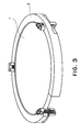
- FIG. 3 illustrates structural features of a supporting structure for an optical element in the projection optical system 42 , according to the first embodiment.
- a lens optical element
- a first holding member for holding the lens. It has a ring-like shape, surrounding the lens.
- a portion of the first holding member 2 is removed, to show how the lens can be held.
- quartz or fluorite is used as a glass material for the lenses, while metal or ceramics having sufficient rigidity and providing high machining precision are used as lens holding members.
- FIG. 4 illustrates the structural features of the first holding member 2 , while a portion thereof is removed.
- the first holding member 2 is formed with three seats 3 which are disposed at approximately 120° pitch. At these three locations, the lens can be supported fixedly. In FIG. 4 , two of the three seats 3 are illustrated. There are holding portions 4 for controlling load deformation, each being placed at an intermediate position between two adjacent seats 3 .
- the structure has three seats and three holding portions (holding members based on a spring or resilient force) for controlling the load deformation.
- a structure with two seats and two holding portions for load deformation control may be used.
- four or more seats and holding portions may be used.
- FIG. 5 is a sectional view, showing details of this portion.
- denoted at 5 is a second holding member for applying a force to the lens.
- Denoted at 6 is a metal spring which functions as a source of supporting force.
- the spring 6 comprises a tension coil spring, having an end connected to the first holding member 2 through a spring supporting member 7 and an adjusting member for adjusting elongation of the spring. The other end is connected to the second holding member 5 .
- the second holding member 5 has a supporting portion 9 for supporting the lens with a predetermined force, a stopper portion 10 , a connection portion being connected to the spring, and a portion 12 (contact portion with the first holding member 2 ) to be contacted to the first holding member 2 to receive action of a balancing force therefrom.
- a level (height) of the adjusting member 8 elongation of the spring, that is, the force applied to the second holding member 5 and, finally, the force to be applied to the lens 2 from the supporting portion 9 , is adjusted.
- the stopper portion 10 is provided to stabilize the attitude of the second holding member 5 during the assemblage even if there is no lens.
- the portion 12 receiving the action of balancing force and the stopper portion 10 which are provided at opposite sides of the spring contact portion 11 , are brought into contact with the first holding member 2 .
- the stopper portion 10 and the first holding member 2 are spaced from each other.
- the structural portions are so arranged that, when a straight line is extended from the connection portion 11 between the spring and the second holding member 5 , in the direction of the action force of the spring and toward a plane which is contained in a triangle defined by the lens supporting portion 9 (single location) and two locations of the balancing force action receiving portions 12 as seen in FIG. 6 , the point of intersection between this straight line and the plane is defined inside the triangle formed by the lens supporting portion 9 and two locations of the balancing force action receiving portion 12 .
- the rigidity K of the lens although it depends on the shape or material used, in an example wherein a convex lens of quartz for use in an exposure apparatus and having a diameter of about 200 mm is used and supported at six locations, the rigidity K defined as described above will be approximately 20000 N/mm. Therefore, if dv/d 1 is calculated while taking L 2 /L 1 approximately equal to 0.5, the result would be 1/100000. This means that, if the spring elongation is adjusted with a resolution 0.1 mm, lens deformation of about 1 nm order can be controlled.
- the necessity of extraordinarily strict precision control for the spring elongation amount can be removed. Without such exact control, but through easy adjustment of the spring elongation amount or appropriate control of the size of each constituent components which are influential to the spring elongation amount, the lens can be supported at six locations of the lens periphery with approximately even forces. Therefore, deformation at the lens peripheral portion due to the lens self-weight as well as deformation of the lens as s whole can be made very small.
- a force to be produced by a member of a shape such as a helical spring shape is applied to the peripheral portion of a lens, made of glass or crystal, in an exact direction as a supporting force, unnecessary friction force or elastic force should be eliminated.
- the second holding member 5 is specifically arranged to meet this. With this arrangement, at the lens holding portions 4 , the resilient force produced by the helical spring is applied exactly and stably as the lens supporting force. By transmitting this supporting force to the first holding member 2 , the whole lens supporting force can be well distributed to six locations uniformly.
- FIG. 7 illustrates the structural features of optical element supporting means according to a second embodiment of the present invention.
- This embodiment is a modified form of the holding portion for holding the lens in the first embodiment. More specifically, there are holding members 21 having a similar function as the second holding member 3 shown in FIG. 3 .
- lens supporting portions 22 with which the lens is supported by the holding member 2 are provided at two locations. Also, there is a portion 23 for receiving the balancing force action is provided at a single location. The remaining portion of this embodiment is basically similar to that of the first embodiment.
- the structural portions are so arranged that, when a straight line is extended from the connection portion 24 with the spring in the direction of the action force of the spring and toward a plane which is contained in a triangle defined by the lens supporting portions 22 (two locations) and the balancing force action receiving portion 23 at a single location, the point of intersection between this straight line and the plane is defined inside the triangle formed by the lens supporting portion 22 and two balancing force action receiving portion 23 .
- the attitude of the holding member 21 can be made stable while the lens is being supported.
- the provision of the second holding member 5 and the holding member 21 having been described with reference to the first and second embodiments is an essential part of the present invention, effective shapes are possible in addition to the shapes shown in FIGS. 6 and 7 .
- a component is provided by which three forces such as an elastic force of a spring, a self-weight force of the lens, and a reaction force from the operational portion provided in the lens supporting member, including a portion for fixedly supporting the lens, are balanced and applied.
- FIGS. 8 and 9 illustrate the structural features of optical element supporting means according to a third embodiment of the present invention, and it concerns a modified form of the lens supporting portion having been described with reference to the first and second embodiments.
- FIG. 8 there are three seats for fixedly supporting a lens, at three locations defined by 120° pitch.
- the lens peripheral portion is supported at total nine locations, in this example.
- These supporting portions at nine locations are disposed along the lens periphery, at regular-pitch angles.
- the supporting force of each holding portion 4 can be set to be equal to 1/9 of the weight of the lens, by adjusting the elongation of the spring.
- supporting portions 4 having a spring are provided at nine locations while fixedly holding portions 3 are provided at three locations.
- the lens is supported at total twelve locations, in this example.
- These twelve supporting portions are disposed along the lens periphery, at regular-pitch angles.
- the supporting force of the holding portion 4 is set to be equal to 1 ⁇ 2 of the weight of the lens.
- the number of locations for supporting the lens periphery is larger than the first embodiment (six locations), and accordingly the flexure deformation at the lens peripheral portion is smaller. Thus, higher precision lens support is possible.
- the seat may be provided at a single location while plural holding portions with springs may be used, to support a lens.
- any seat is not used but three or more holding portions with springs may be provided to support a lens. If a lens is supported only by use of holding portions having springs, preferably four or more supporting portions and, more desirably, six or more supporting portions should be provided.
- FIG. 10 illustrates the structural features of an elastic force adjusting mechanism for adjusting the elastic force of an elastic member, in a fourth embodiment of the present invention.
- denoted at 41 is a mechanism for adjusting elongation of a spring, and it functions to adjust the amount of spring elongation by adjusting the position of a spring supporting member 7 , for supporting an upper end portion of a spring 6 , with use of a screw and a nut.
- this embodiment uses an adjusting mechanism based on a screw and a nut, as a mechanism for adjusting the position, a structure for sandwiching an adjusting member such as that of the first embodiment may be used and the thickness of the adjusting member may be chosen.
- the adjusting member may be provided by two wedge members so that the thickness of the adjusting member can be adjusted by these wedge members.
- the first embodiment has been described with reference to an example wherein the amount of this adjustment is set so that, at respective supporting positions, the lens supporting forces become even.
- this adjusting function may be utilized specifically for modification or correction in the lens system. For example, after the lens surface shape is observed, a deformation force to be applied to the peripheral portion of the lens as required to obtain a desired lens surface shape may be calculated. Then, the spring elongation amount may be adjusted to provide corresponding lens supporting forces. A desired surface shape can be accomplished thereby.
- the spring elongation may be adjusted while directly observing the lens surface shape.
- a desired surface shape can be accomplished thereby.
- the lens supporting positions at three locations may be held fixed, and adjusting portions may be defined at three locations each being between adjacent fixed supporting positions. In such structure, by applying the same amount of adjustment at the three adjusting positions, respectively, three ⁇ components of the lens surface shape can be adjusted.
- the lens supporting structure of FIG. 10 may be applied to an appropriate lens or lenses in a lens system such as an imaging optical system having a plurality of lenses.
- the lens supporting may be adjusted to provide best performance of the lens system or appropriate aberration of it.
- the lens surface shape may be changed to adjust three 0 component of the wavefront of aberration, or field distortion (distortion).
- FIG. 11 is a schematic view of a semiconductor exposure system according to a fifth embodiment of the present invention.
- the exposure system is provided with an exposure optical system having a lens system in which lens supporting means described with reference to the preceding embodiments is incorporated.
- lens supporting means described with reference to the preceding embodiments
- the lens system is provided with driving means 71 such that the adjustment can be done by actuator drive.
- the exposure apparatus is provided with means 72 for expecting a change in aberration of the exposure optical system.
- This means may comprise means for directly measuring aberration of the exposure optical system or, alternatively, it may be means for indirectly obtaining information such as temperature information of the exposure optical system, for example.
- information may be supplied to a computer 73 to calculate a value necessary for obtaining a driving amount for the driving means in the lens system, in regard to the position, attitude and deformation or the like of the lenses.
- the computer 73 supplies appropriate driving signals to respective correcting means in the optical system, including those having been described hereinbefore, thereby to correct the optical system so as to reduce the aberration. With these adjustments, best transfer performance of the exposure apparatus can be maintained.
- the optical element may be a mirror, other than a lens.
- the invention is applicable also to an optical element wherein deformation should be considered, such as an optical element based on diffraction, for example.
- the invention is applicable to various optical systems having a high precision optical system.
- FIGS. 12 and 13 an embodiment of a device manufacturing method which uses an exposure apparatus based on the fifth embodiment described above, will be explained.
- FIG. 12 is a flow chart for explaining the procedure of manufacturing various microdevices such as semiconductor chips (e.g., ICs or LSIs), liquid crystal panels, or CCDs, for example.
- semiconductor chips e.g., ICs or LSIs
- Step 1 is a design process for designing a circuit of a semiconductor device.
- Step 2 is a process for making a mask on the basis of the circuit pattern design.
- Step 3 is a process for preparing a wafer by using a material such as silicon.
- Step 4 is a wafer process which is called a pre-process wherein, by using the thus prepared mask and wafer, a circuit is formed on the wafer in practice, in accordance with lithography.
- Step 5 subsequent to this is an assembling step which is called a post-process wherein the wafer having been processed at step 4 is formed into semiconductor chips.
- This step includes an assembling (dicing and bonding) process and a packaging (chip sealing) process.
- Step 6 is an inspection step wherein an operation check, a durability check an so on, for the semiconductor devices produced by step 5 , are carried out. With these processes, semiconductor devices are produced, and they are shipped (step 7 ).
- FIG. 13 is a flow chart for explaining details of the wafer process.
- Step 11 is an oxidation process for oxidizing the surface of a wafer.
- Step 12 is a CVD process for forming an insulating film on the wafer surface.
- Step 13 is an electrode forming process for forming electrodes upon the wafer by vapor deposition.
- Step 14 is an ion implanting process for implanting ions to the wafer.
- Step 15 is a resist process for applying a resist (photosensitive material) to the wafer.
- Step 16 is an exposure process for printing, by exposure, the circuit pattern of the mask on the wafer through the exposure apparatus described above.
- Step 17 is a developing process for developing the exposed wafer.
- Step 18 is an etching process for removing portions other than the developed resist image.
- Step 19 is a resist separation process for separating the resist material remaining on the wafer after being subjected to the etching process. By repeating these processes, circuit patterns are superposedly formed on the wafer.
- a supporting structure for an optical element by which, when the optical element is supported, distortion in shape of the optical element attributable to a difference in thermal expansion between the optical element and a supporting member for supporting the same or to the assembling of the optical element can be prevented effectively.
- an optical system having such optical element supporting structure, a method of adjusting an optical system, an exposure apparatus, an exposure method and a device manufacturing method can be accomplished.
Landscapes
- Physics & Mathematics (AREA)
- Health & Medical Sciences (AREA)
- General Physics & Mathematics (AREA)
- Epidemiology (AREA)
- Engineering & Computer Science (AREA)
- Environmental & Geological Engineering (AREA)
- Public Health (AREA)
- Toxicology (AREA)
- Atmospheric Sciences (AREA)
- Life Sciences & Earth Sciences (AREA)
- Optics & Photonics (AREA)
- Exposure Of Semiconductors, Excluding Electron Or Ion Beam Exposure (AREA)
- Exposure And Positioning Against Photoresist Photosensitive Materials (AREA)
- Lens Barrels (AREA)
- Mounting And Adjusting Of Optical Elements (AREA)
Applications Claiming Priority (2)
| Application Number | Priority Date | Filing Date | Title |
|---|---|---|---|
| JP2002232499A JP4174262B2 (ja) | 2002-08-09 | 2002-08-09 | 光学要素の支持構造、光学系、光学系の調整方法、露光装置、露光方法、半導体デバイス製造方法 |
| JP232499/2002(PAT.) | 2002-08-09 |
Publications (2)
| Publication Number | Publication Date |
|---|---|
| US20040105177A1 US20040105177A1 (en) | 2004-06-03 |
| US7136238B2 true US7136238B2 (en) | 2006-11-14 |
Family
ID=32017883
Family Applications (1)
| Application Number | Title | Priority Date | Filing Date |
|---|---|---|---|
| US10/637,345 Expired - Lifetime US7136238B2 (en) | 2002-08-09 | 2003-08-08 | Method of supporting and adjusting optical element in exposure apparatus |
Country Status (2)
| Country | Link |
|---|---|
| US (1) | US7136238B2 (ja) |
| JP (1) | JP4174262B2 (ja) |
Families Citing this family (4)
| Publication number | Priority date | Publication date | Assignee | Title |
|---|---|---|---|---|
| DE10140608A1 (de) * | 2001-08-18 | 2003-03-06 | Zeiss Carl | Vorrichtung zur Justage eines optischen Elements |
| DE102009029536A1 (de) * | 2008-09-17 | 2010-04-15 | Carl Zeiss Smt Ag | Verbindungsanordnung für eine optische Einrichtung |
| US11056803B2 (en) * | 2017-09-12 | 2021-07-06 | Lumentum Operations Llc | Spring clamp for optics |
| CN113917645B (zh) * | 2021-11-01 | 2023-03-31 | 中国科学院光电技术研究所 | 一种镜片弹性支撑装置 |
Citations (3)
| Publication number | Priority date | Publication date | Assignee | Title |
|---|---|---|---|---|
| US6086209A (en) * | 1998-04-20 | 2000-07-11 | Sony Corporation | Mirror holder and optical axis correcting device using the same |
| US6307688B1 (en) * | 1998-12-23 | 2001-10-23 | Carl-Zeiss-Stiftung | Optical system, in particular projection-illumination unit used in microlithography |
| US6400516B1 (en) * | 2000-08-10 | 2002-06-04 | Nikon Corporation | Kinematic optical mounting |
-
2002
- 2002-08-09 JP JP2002232499A patent/JP4174262B2/ja not_active Expired - Fee Related
-
2003
- 2003-08-08 US US10/637,345 patent/US7136238B2/en not_active Expired - Lifetime
Patent Citations (3)
| Publication number | Priority date | Publication date | Assignee | Title |
|---|---|---|---|---|
| US6086209A (en) * | 1998-04-20 | 2000-07-11 | Sony Corporation | Mirror holder and optical axis correcting device using the same |
| US6307688B1 (en) * | 1998-12-23 | 2001-10-23 | Carl-Zeiss-Stiftung | Optical system, in particular projection-illumination unit used in microlithography |
| US6400516B1 (en) * | 2000-08-10 | 2002-06-04 | Nikon Corporation | Kinematic optical mounting |
Also Published As
| Publication number | Publication date |
|---|---|
| JP4174262B2 (ja) | 2008-10-29 |
| JP2004070192A (ja) | 2004-03-04 |
| US20040105177A1 (en) | 2004-06-03 |
Similar Documents
| Publication | Publication Date | Title |
|---|---|---|
| US7345834B2 (en) | Optical element holding system, barrel, exposure apparatus, and device manufacturing method | |
| US7746575B2 (en) | Support mechanism, exposure apparatus having the same, and aberration reducing method | |
| US7218383B2 (en) | Holding system, exposure apparatus, and device manufacturing method | |
| US7352520B2 (en) | Holding device and exposure apparatus using the same | |
| US20060072219A1 (en) | Mirror holding mechanism in exposure apparatus, and device manufacturing method | |
| US7525639B2 (en) | Exposure apparatus and method, and device manufacturing method using the same | |
| US20060056038A1 (en) | Aberration correcting optical system | |
| US4676631A (en) | Device for adjusting projection magnification | |
| JP2008112756A (ja) | 光学素子駆動装置及びその制御方法、露光装置、並びにデバイス製造方法 | |
| US20050230599A1 (en) | Illumination optical system, exposure apparatus, and device manufacturing method using the same | |
| US7031082B2 (en) | Retainer, exposure apparatus, and device fabrication method | |
| US6459534B1 (en) | Projection optical system and projection exposure apparatus with the same, and device manufacturing method | |
| US6069931A (en) | Mask structure and mask holding mechanism for exposure apparatus | |
| US20050122502A1 (en) | Exposure apparatus | |
| US7136238B2 (en) | Method of supporting and adjusting optical element in exposure apparatus | |
| US6909493B2 (en) | Correction member, retainer, exposure apparatus, and device fabrication method | |
| US6621555B1 (en) | Projection optical system and projection exposure apparatus with the same, and device manufacturing method | |
| JP2013106017A (ja) | 光学素子保持装置、光学装置、及び露光装置 | |
| JP2011035102A (ja) | 光学素子の保持装置、それを用いた露光装置、及びデバイスの製造方法 | |
| JP5335372B2 (ja) | 光学要素の支持装置、それを用いた露光装置及びデバイスの製造方法 | |
| US7583453B2 (en) | Optical element holding structure, exposure apparatus, and device manufacturing method | |
| US20110065051A1 (en) | Supporting device, optical apparatus, exposure apparatus, and device manufacturing method | |
| JP2000195784A (ja) | 露光装置およびデバイス製造方法 | |
| WO2022248433A1 (en) | Projection exposure apparatus and method for designing a component of a projection exposure apparatus | |
| JP2003344741A (ja) | 補正部材、保持装置、露光装置及びデバイス製造方法 |
Legal Events
| Date | Code | Title | Description |
|---|---|---|---|
| AS | Assignment |
Owner name: CANON KABUSHIKI KAISHA, JAPAN Free format text: ASSIGNMENT OF ASSIGNORS INTEREST;ASSIGNOR:EBINUMA, RYUICHI;REEL/FRAME:014864/0736 Effective date: 20031128 |
|
| STCF | Information on status: patent grant |
Free format text: PATENTED CASE |
|
| FEPP | Fee payment procedure |
Free format text: PAYER NUMBER DE-ASSIGNED (ORIGINAL EVENT CODE: RMPN); ENTITY STATUS OF PATENT OWNER: LARGE ENTITY Free format text: PAYOR NUMBER ASSIGNED (ORIGINAL EVENT CODE: ASPN); ENTITY STATUS OF PATENT OWNER: LARGE ENTITY |
|
| FPAY | Fee payment |
Year of fee payment: 4 |
|
| FPAY | Fee payment |
Year of fee payment: 8 |
|
| MAFP | Maintenance fee payment |
Free format text: PAYMENT OF MAINTENANCE FEE, 12TH YEAR, LARGE ENTITY (ORIGINAL EVENT CODE: M1553) Year of fee payment: 12 |