US6997769B2 - Plasma display panel manufacturing apparatus and manufacturing method - Google Patents
Plasma display panel manufacturing apparatus and manufacturing method Download PDFInfo
- Publication number
- US6997769B2 US6997769B2 US09/755,696 US75569601A US6997769B2 US 6997769 B2 US6997769 B2 US 6997769B2 US 75569601 A US75569601 A US 75569601A US 6997769 B2 US6997769 B2 US 6997769B2
- Authority
- US
- United States
- Prior art keywords
- gas introduction
- display panel
- plasma display
- chamber
- gas
- Prior art date
- Legal status (The legal status is an assumption and is not a legal conclusion. Google has not performed a legal analysis and makes no representation as to the accuracy of the status listed.)
- Expired - Fee Related, expires
Links
Images


Classifications
-
- H—ELECTRICITY
- H01—ELECTRIC ELEMENTS
- H01J—ELECTRIC DISCHARGE TUBES OR DISCHARGE LAMPS
- H01J9/00—Apparatus or processes specially adapted for the manufacture, installation, removal, maintenance of electric discharge tubes, discharge lamps, or parts thereof; Recovery of material from discharge tubes or lamps
- H01J9/46—Machines having sequentially arranged operating stations
-
- H—ELECTRICITY
- H01—ELECTRIC ELEMENTS
- H01J—ELECTRIC DISCHARGE TUBES OR DISCHARGE LAMPS
- H01J9/00—Apparatus or processes specially adapted for the manufacture, installation, removal, maintenance of electric discharge tubes, discharge lamps, or parts thereof; Recovery of material from discharge tubes or lamps
- H01J9/24—Manufacture or joining of vessels, leading-in conductors or bases
- H01J9/26—Sealing together parts of vessels
- H01J9/261—Sealing together parts of vessels the vessel being for a flat panel display
-
- H—ELECTRICITY
- H01—ELECTRIC ELEMENTS
- H01J—ELECTRIC DISCHARGE TUBES OR DISCHARGE LAMPS
- H01J11/00—Gas-filled discharge tubes with alternating current induction of the discharge, e.g. alternating current plasma display panels [AC-PDP]; Gas-filled discharge tubes without any main electrode inside the vessel; Gas-filled discharge tubes with at least one main electrode outside the vessel
- H01J11/20—Constructional details
-
- H—ELECTRICITY
- H01—ELECTRIC ELEMENTS
- H01J—ELECTRIC DISCHARGE TUBES OR DISCHARGE LAMPS
- H01J9/00—Apparatus or processes specially adapted for the manufacture, installation, removal, maintenance of electric discharge tubes, discharge lamps, or parts thereof; Recovery of material from discharge tubes or lamps
- H01J9/24—Manufacture or joining of vessels, leading-in conductors or bases
-
- H—ELECTRICITY
- H01—ELECTRIC ELEMENTS
- H01J—ELECTRIC DISCHARGE TUBES OR DISCHARGE LAMPS
- H01J9/00—Apparatus or processes specially adapted for the manufacture, installation, removal, maintenance of electric discharge tubes, discharge lamps, or parts thereof; Recovery of material from discharge tubes or lamps
- H01J9/38—Exhausting, degassing, filling, or cleaning vessels
-
- H—ELECTRICITY
- H01—ELECTRIC ELEMENTS
- H01J—ELECTRIC DISCHARGE TUBES OR DISCHARGE LAMPS
- H01J2209/00—Apparatus and processes for manufacture of discharge tubes
- H01J2209/26—Sealing parts of the vessel to provide a vacuum enclosure
- H01J2209/261—Apparatus used for sealing vessels, e.g. furnaces, machines or the like
Definitions
- the present invention relates to a plasma display panel manufacturing apparatus, and to a manufacturing method therefor, and more particularly to an apparatus for performing integrated panel sealing, release of exhaust gas, introduction of luminescent gas or discharge gas, and vacuum sealing, and a method of manufacturing a plasma display panel using this apparatus.
- a plasma display panel is generally formed by a front substrate and a rear substrate which have mutually perpendicular opposing electrodes on each of the substrates, a glass tube (hereinafter referred to as an exhaust tube) mounted by low-melting-point glass so as to join a through hole provided beforehand on the rear substrate for the purpose of introducing and exhausting gas, these elements being placed in a sealing furnace so as to melt the low-melting-point glass and form the glass vessel.
- the panel is heated to release internal gas.
- filling is done with a gas such as neon (Ne), argon (Ar), or xenon (Xe) or a gas mixture thereof at approximately 53,200 to 79,800 Pa (400 to 600 Torr), which serves as a luminescent gas, after which a gas burner or the like is used to seal the exhaust tube thereby forming a plasma display panel with an exhaust tube.
- a gas such as neon (Ne), argon (Ar), or xenon (Xe) or a gas mixture thereof at approximately 53,200 to 79,800 Pa (400 to 600 Torr)
- a gas burner or the like is used to seal the exhaust tube thereby forming a plasma display panel with an exhaust tube.
- a second known method is that of combining a rear substrate and a front substrate, and placing the combination inside a vacuum chamber, performing vacuum exhausting and degassing, and subsequent filling with a luminescent gas in the vacuum chamber, and then melting the low-melting-point glass of the peripheral part of the substrate so as to perform sealing thereof.
- the structure is one in which there is neither an exhaust tube nor a gas introduction hole in the panel.
- a third method that has been proposed is one in which a 10 to 20 mm semichip tube is provided as a gas introduction hole, this semichip tube provided on the substrate being covered by a small chamber, and residual gas within the panel being exhausted via the semichip tube, after which gas sealing is done, a halogen lamp being used to illuminate the semichip tube via a quartz window provided in the small chamber, so as to melt the semichip tube and perform sealing.
- the glass tube (chip tube) remaining after the exhaust tube is removed is extremely fragile, and subject to breakage with even a small shock, not only is it necessary to take extreme care when handling the panel, but also when the plasma display panel is combined with a driving electronic circuit to form a module, it is necessary to mount a protective cap, and to establish a design that avoids interference in electronic components and the printed circuit board.
- the present invention has the following basic technical constitution.
- a first aspect of the present invention is an apparatus for manufacturing a plasma display panel comprising a joining chamber that forms a plasma display panel by joining a front substrate and a rear substrate by heating a low-melting-point glass and a gas introduction and sealing chamber which introduces a luminescent gas into the plasma display panel which is formed by the joining chamber via a gas introduction port provided in the front substrate or the rear substrate, and seals the gas introduction port, the manufacturing apparatus further comprising: a first mechanism for supplying a cover member formed by a metal sheet to which low-melting-point glass is applied to a first location within the gas introduction and sealing chamber, a second mechanism provided in the gas introduction and sealing chamber for moving the cover member from the first location to a second location which is over a heating apparatus, a third mechanism provided in the gas introduction and sealing chamber for performing vacuum exhausting an inside of the plasma display panel and introducing a luminescent gas into the plasma display panel, and a fourth mechanism provided in the gas introduction and sealing chamber for heating the metal sheet to which the low-melting
- a first member movable up and down disposed within the gas introduction and sealing chamber, and a second member movable up and down which is surrounded by the first member are provided, the fourth mechanism is provided on the second member, and the third mechanism is provided in the first member.
- a plasma display panel in which the front substrate is fixed to the rear substrate is placed within the joining chamber, and the joining chamber is vacuum-exhausted and the front substrate and the rear substrate are joined by the low-melting-point glass.
- the joining chamber and the gas introduction and sealing chamber are a single chamber.
- a luminescent gas introduction system and a gas exhaust system are provided in the gas introduction and sealing chamber, and the luminescent gas introduction system and the gas exhaust system are communicating with the gas introduction/exhaust path provided inside the second member.
- one end of the second member is brought into intimate contact with the plasma display panel.
- a method for manufacturing a plasma display panel according to the present invention is a method for manufacturing a plasma display panel formed by heating a low-melting-point glass so as to join a front substrate to a rear substrate, after which a luminescent gas is introduced into the plasma display panel via a gas introduction port provided in either the front substrate or the rear substrate, after which the gas introduction port is sealed, the method comprising: a first step of fixing the front substrate of said plasma display panel to the rear substrates, placing the substrates into a joining chamber, and then performing vacuum exhausting an inside of the joining chamber, a second step of heating a sealing glass provided on the front substrate or the rear substrate, so as to join the front substrate to the rear substrate, a third step of placing the joined plasma display panel in a gas introduction and sealing chamber which has been vacuum-exhausted, and then vacuum exhausting an inside of the plasma display panel, a fourth step of making an inside of the gas introduction and sealing chamber an atmospheric pressure, a fifth step of introducing the luminescent gas into the plasma display panel which has been vacuum-
- the sixth step comprising: a step of supplying a cover member formed by a metal sheet to which a low-melting-point glass is applied to a first location within the gas introduction and sealing chamber, a step of moving the cover member to a second location which is over a heating apparatus provided within the gas introduction and sealing chamber, and a step of pressing the metal sheet to which is applied a low-melting-point glass on the heating apparatus against the gas introduction port and sealing the gas introduction port.
- FIG. 1 is a drawing showing the configuration of an apparatus for manufacturing a plasma display panel according to the present invention.
- FIG. 2 is a cross-sectional view showing details of the configuration of a cover member stocking mechanism, cover member moving mechanism, a small chamber provided in the gas introduction and sealing chamber.
- FIG. 3 is a drawing shown the condition in which the cap of the small chamber is brought into intimate contact with the plasma display panel, and the inside of the panel is exhausted or filled with a luminescent gas.
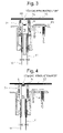
- FIG. 4 is a drawing which shows the condition in which the heating apparatus in the small chamber is pushed up, a cover member is pushed up against the gas introduction port of the plasma display panel, and the gas introduction port is sealed.
- FIG. 5 is a flowchart showing the process steps of the present invention.
- FIG. 1 to FIG. 5 illustrate an apparatus and a method for manufacturing a plasma display panel according to the present invention, these drawings showing an apparatus for manufacturing a plasma display panel, this apparatus having a joining chamber 1 in which the front and rear substrates are joined by heating a low-melting-point glass, thereby forming the plasma display panel, and a gas introduction and sealing chamber 2 , in which a luminescent gas or discharge gas is introduced into the plasma display panel via a gas introduction port 13 a provided in the front substrate or the rear substrate, after which the as introduction port is sealed.
- a first mechanism 5 for supplying a cover member 9 made of a metal sheet to which a low-melting-point glass is applied to a prescribed position P 1 inside the gas introduction and sealing chamber 2 , a second mechanism 4 for moving the cover member 9 from the prescribed position P 1 to over a heating apparatus 8 , a third mechanism 31 for vacuum exhausting the inside of the plasma display panel and then introducing a luminescent gas into the plasma display panel, and a fourth mechanism 41 for heating with the heating apparatus 8 the cover member 9 to which a low-melting-point glass is applied so as to seal the gas introduction port 13 a.
- a first up/down moving member 7 is provided inside a small chamber 3 provided within the gas introduction and sealing chamber 2 , and a second up/down moving member 42 is provided so as to be surrounded within the first member 7 , the fourth mechanism 41 being assembled with the second member 42 , and the third mechanism 31 being assembled with the first member 7 .
- an apparatus for manufacturing a plasma display panel in which a plasma display panel with an assembled front substrate and rear substrate is placed inside the joining chamber 1 , a vacuum exhausting mechanism 1 a for vacuum exhausting within the joining chamber 1 being further provided.
- FIG.1 shows the configuration of an apparatus for manufacturing a plasma display panel according to the present invention
- FIG. 2 is an enlarged cross-sectional view showing the main part of the gas introduction and sealing chamber
- FIG. 3 is a cross-sectional view showing the condition in which a cap is pushed upward, and the plasma display panel is vacuum exhausted or filled with a luminescent gas
- FIG. 4 is a drawing showing the condition in which a heater is pressed up against the gas introduction port of the plasma display panel.
- the gas introduction and sealing chamber 2 is provided next to the joining chamber 1 , and a small chamber 3 , a cover member moving mechanism 4 , and a cover member stocking mechanism 5 are further provided within the gas introduction and sealing chamber 2 .
- the cover member stocking mechanism 5 is configured so that it constantly supplies a metal cover member 9 to the position P 1 in the gas introduction and sealing chamber 2 .
- the metal cover member 9 is formed of an iron-nickel-chromium alloy such as 426 alloy which is wet hydrogen processed to form a chrome-rich oxide film thereon, on one side of which a low-melting-point lead glass layer having a working temperature of 430° C. is applied and fused.
- the cover member moving mechanism 4 moves a metal cover member 9 placed at the position P 1 to a position P 2 over a heater 8 provided in the small chamber 3 , and has on its end a transporting arm 6 to which is mounted an electromagnet, the arm 6 being driven by an up/down rotating mechanism (not shown in the drawing).
- a cylindrical exhausting/gas introduction member (hereinafter referred to as the cap) 7 that moves up and down is provided within the small chamber 3 , and an O-ring 12 for providing an intimate contact between the end part of the cap 7 and the plasma display panel 13 is mounted on the end part of the cap 7 .
- the luminescent gas introduction system 10 and the exhaust system 11 are provided, and the luminescent gas introduction system 10 and the exhaust system 11 are communicating with the gas introduction/exhaust path 7 a provided inside the cap 7 .
- the cap 7 is vacuum-sealed with respect to the outside atmosphere by an O-ring double seal 12 a that is movable up and down.
- a rod-shaped member 42 is provided inside the cap 7 , the top part of this rod-shaped member 42 having a heater 8 mounted thereto, the rod-shaped member 42 being movable up and down, and vacuum sealed with respect to the outside atmosphere by an O-ring double seal 12 b.
- a method for manufacturing a plasma display panel according to the present invention is described below, with reference made to the FIG. 3 , FIG. 4 , and the flowchart of FIG. 5 .
- a transparent electrode, a bus electrode, a transparent dielectric layer, and a MgO protective layer and so forth are formed on the surface of the front substrate of the plasma display panel, and a data electrode, transparent dielectric layer, a separator, a phosphor layer, and a sealing glass layer and so forth are formed on the rear substrate thereof.
- a gas introduction port which is a through hole for the purpose of exhaust gas release and introduction of a luminescent gas is additionally provided on the rear substrate.
- the two substrates are assembled in mutual opposition and are temporarily held together using, for example, a fixture or clip (step S 1 ).
- the temporarily joined substrates are placed in the joining chamber 1 shown in FIG. 1 (step S 2 ), exhausting is done by an exhausting apparatus 1 a , and gas is released and joining is performed, using a heater (not shown in the drawing) (steps S 3 and S 4 ).
- the gas introduction and sealing chamber 2 shown in FIG. 1 is vacuum exhausted (step S 5 ), a metal cover member 9 stocked in the cover member stocking mechanism 5 is moved to over the heater 8 by the cover member moving mechanism 4 (step S 6 ), and pre-heating is done with the heater (step S 7 ).
- the joined panel is moved from the joining chamber 1 to the gas introduction and sealing chamber 2 (step S 8 ).
- the gas introduction port of the rear substrate is positioned near the center line of the heater 8 .
- the luminescent gas introduction system 10 introduces a luminescent gas mixture of argon (Ar), neon (Ne), and xenon (Xe), via the opening 7 b , at a specified pressure of 53,200 to 79,800 Pa (400 to 600 Torr) (step S 11 ).
- FIG. 3 shows the above noted condition in which a cap is pushed upward, and the plasma display panel is vacuum exhausted or filled with a luminescent gas.
- step S 12 as the heater is heated (step S 12 ), the heater 8 is pushed upward, so as to seal the gas introduction port of the rear substrate 13 with low-melting-point glass (step S 13 ).
- step S 14 the heater is lowered (step S 14 ), the cap 7 being lowered and the gas introduction and sealing chamber 2 is leaked so as to be at atmospheric pressure (step S 15 ).
- step S 15 The panel is moved to an unloader, and cooled to below 100° C. (step S 16 ), after which the plasma display panel is removed from the unloader (step S 17 ).
- an apparatus and a method for manufacturing a plasma display panel achieves the following effects.
- the luminescent gas is introduced into the panel via a luminescent gas introduction system provided in the small chamber, there is no need to fill a large-capacity vacuum chamber with the luminescent gas, thereby enabling a savings in the amount of high-cost luminescent gas used.
- the gas introduction port is sealed by a low-melting-point glass and a metal sheet, there is no chip tube protrusion remaining on the panel, thereby solving the problems involved in handling the panel.
Landscapes
- Engineering & Computer Science (AREA)
- Manufacturing & Machinery (AREA)
- Physics & Mathematics (AREA)
- Plasma & Fusion (AREA)
- Manufacture Of Electron Tubes, Discharge Lamp Vessels, Lead-In Wires, And The Like (AREA)
- Gas-Filled Discharge Tubes (AREA)
- Devices For Indicating Variable Information By Combining Individual Elements (AREA)
Abstract
Description
Claims (5)
Priority Applications (1)
| Application Number | Priority Date | Filing Date | Title |
|---|---|---|---|
| US11/291,984 US20060084349A1 (en) | 2000-01-07 | 2005-12-02 | Plasma display panel manufacturing apparatus and manufacturing method |
Applications Claiming Priority (2)
| Application Number | Priority Date | Filing Date | Title |
|---|---|---|---|
| JP2000001842A JP3440906B2 (en) | 2000-01-07 | 2000-01-07 | Apparatus and method for manufacturing plasma display panel |
| JP2000-1842 | 2000-01-07 |
Related Child Applications (1)
| Application Number | Title | Priority Date | Filing Date |
|---|---|---|---|
| US11/291,984 Division US20060084349A1 (en) | 2000-01-07 | 2005-12-02 | Plasma display panel manufacturing apparatus and manufacturing method |
Publications (2)
| Publication Number | Publication Date |
|---|---|
| US20010007805A1 US20010007805A1 (en) | 2001-07-12 |
| US6997769B2 true US6997769B2 (en) | 2006-02-14 |
Family
ID=18531025
Family Applications (2)
| Application Number | Title | Priority Date | Filing Date |
|---|---|---|---|
| US09/755,696 Expired - Fee Related US6997769B2 (en) | 2000-01-07 | 2001-01-05 | Plasma display panel manufacturing apparatus and manufacturing method |
| US11/291,984 Abandoned US20060084349A1 (en) | 2000-01-07 | 2005-12-02 | Plasma display panel manufacturing apparatus and manufacturing method |
Family Applications After (1)
| Application Number | Title | Priority Date | Filing Date |
|---|---|---|---|
| US11/291,984 Abandoned US20060084349A1 (en) | 2000-01-07 | 2005-12-02 | Plasma display panel manufacturing apparatus and manufacturing method |
Country Status (3)
| Country | Link |
|---|---|
| US (2) | US6997769B2 (en) |
| JP (1) | JP3440906B2 (en) |
| KR (1) | KR100406840B1 (en) |
Cited By (4)
| Publication number | Priority date | Publication date | Assignee | Title |
|---|---|---|---|---|
| US20050075031A1 (en) * | 2003-10-07 | 2005-04-07 | Canon Kabushiki Kaisha | Electron source manufacturing apparatus and electron source manufacturing method |
| US20080040916A1 (en) * | 2006-08-21 | 2008-02-21 | Adp Engineering Co., Ltd. | Apparatus for attaching substrates of flat display panel |
| US20080074030A1 (en) * | 2004-11-01 | 2008-03-27 | Jeong Keun Chu | Flat Display Panel Having Exhaust Holes Within Display Area |
| TWI457876B (en) * | 2008-09-04 | 2014-10-21 | Shibaura Mechatronics Corp | Fit the device |
Families Citing this family (9)
| Publication number | Priority date | Publication date | Assignee | Title |
|---|---|---|---|---|
| KR20080105787A (en) * | 2007-06-01 | 2008-12-04 | 엘지전자 주식회사 | Plasma Display Panel And Method Of Manufacturing The Same |
| WO2008153359A2 (en) * | 2007-06-13 | 2008-12-18 | Kt Freetel Co., Ltd. | Power allocation method and mobile communication system using the same |
| JP5078772B2 (en) * | 2007-07-26 | 2012-11-21 | キヤノン株式会社 | Airtight container and image display device manufacturing method |
| CN101587808B (en) * | 2008-05-23 | 2011-06-08 | 清华大学 | Sealing device and sealing method of vacuum devices |
| CN101609773B (en) * | 2008-06-18 | 2012-05-16 | 清华大学 | Method for sealing vacuum device |
| JP5252301B2 (en) * | 2009-04-06 | 2013-07-31 | 株式会社アルバック | Plasma display panel sealing method, sealing mechanism, and sealing device |
| JP4773552B2 (en) * | 2009-08-20 | 2011-09-14 | 中外炉工業株式会社 | Vacuum exhaust head |
| DE102011008886A1 (en) | 2011-01-19 | 2012-07-19 | Sterrix Technologies UG (haftungsbeschränkt) | Method and apparatus for stereobase extension of stereoscopic images and image sequences |
| KR101541124B1 (en) | 2013-08-27 | 2015-08-06 | 주식회사 좋은기술 | Sealing apparatus of manufacturing equipment for vacuum window |
Citations (19)
| Publication number | Priority date | Publication date | Assignee | Title |
|---|---|---|---|---|
| JPS63207033A (en) | 1987-02-24 | 1988-08-26 | Nec Kagoshima Ltd | Manufacturing equipment for character display tube |
| JPH02299130A (en) | 1989-05-15 | 1990-12-11 | Canon Inc | Manufacture of flat display |
| JPH04298944A (en) | 1991-03-28 | 1992-10-22 | Matsushita Electric Ind Co Ltd | Manufacturing device and method for flat display device |
| JPH0548354A (en) | 1991-08-19 | 1993-02-26 | Matsushita Electric Ind Co Ltd | Gain control circuit and semiconductor device |
| US5207607A (en) * | 1990-04-11 | 1993-05-04 | Mitsubishi Denki Kabushiki Kaisha | Plasma display panel and a process for producing the same |
| JPH069437A (en) | 1992-06-22 | 1994-01-18 | Mitsui Petrochem Ind Ltd | Production of tetracyclododecene |
| JPH06139935A (en) | 1992-06-22 | 1994-05-20 | Nec Corp | Manufactring device for diplay tube |
| US5797780A (en) * | 1996-02-23 | 1998-08-25 | Industrial Technology Research Institute | Hybrid tubeless sealing process for flat panel displays |
| US5813893A (en) * | 1995-12-29 | 1998-09-29 | Sgs-Thomson Microelectronics, Inc. | Field emission display fabrication method |
| US5846110A (en) * | 1995-06-30 | 1998-12-08 | Fujitsu Limited | Method of manufacturing plasma display panels with convex surface |
| US5876260A (en) * | 1994-11-09 | 1999-03-02 | Pixtech Sa | Method for assembling a flat display screen |
| JPH11204039A (en) | 1998-01-12 | 1999-07-30 | Nec Kagoshima Ltd | Evacuation apparatus of fluorescent character display tube |
| US5938494A (en) * | 1996-11-20 | 1999-08-17 | Fujitsu Limited | Method for producing a plasma display panel |
| US6172460B1 (en) * | 1998-06-05 | 2001-01-09 | U.S. Philips Corporation | Display device |
| US6186722B1 (en) * | 1997-02-26 | 2001-02-13 | Fujitsu Limited | Chamber apparatus for processing semiconductor devices |
| US6193811B1 (en) * | 1999-03-03 | 2001-02-27 | Applied Materials, Inc. | Method for improved chamber bake-out and cool-down |
| US6254449B1 (en) * | 1997-08-29 | 2001-07-03 | Canon Kabushiki Kaisha | Manufacturing method of image forming apparatus, manufacturing apparatus of image forming apparatus, image forming apparatus, manufacturing method of panel apparatus, and manufacturing apparatus of panel apparatus |
| US6257945B1 (en) * | 1997-01-16 | 2001-07-10 | Sony Corporation | Method for sealing a gas within a picture display device |
| US6719516B2 (en) * | 1998-09-28 | 2004-04-13 | Applied Materials, Inc. | Single wafer load lock with internal wafer transport |
Family Cites Families (4)
| Publication number | Priority date | Publication date | Assignee | Title |
|---|---|---|---|---|
| JP3372848B2 (en) * | 1996-10-31 | 2003-02-04 | キヤノン株式会社 | Electron emitting device, image display device, and manufacturing method thereof |
| JP3465634B2 (en) * | 1998-06-29 | 2003-11-10 | 富士通株式会社 | Method for manufacturing plasma display panel |
| KR100723751B1 (en) * | 2000-01-26 | 2007-05-30 | 마츠시타 덴끼 산교 가부시키가이샤 | Gas discharge light emitting device and its manufacturing method |
| US6828588B2 (en) * | 2000-07-12 | 2004-12-07 | Mitsubishi Materials Corporation | Protective film for FPD, vapor deposition material for protective film and its production method, FPD, and manufacturing device for FPD protective film |
-
2000
- 2000-01-07 JP JP2000001842A patent/JP3440906B2/en not_active Expired - Fee Related
-
2001
- 2001-01-05 US US09/755,696 patent/US6997769B2/en not_active Expired - Fee Related
- 2001-01-05 KR KR10-2001-0000509A patent/KR100406840B1/en not_active Expired - Fee Related
-
2005
- 2005-12-02 US US11/291,984 patent/US20060084349A1/en not_active Abandoned
Patent Citations (20)
| Publication number | Priority date | Publication date | Assignee | Title |
|---|---|---|---|---|
| JPS63207033A (en) | 1987-02-24 | 1988-08-26 | Nec Kagoshima Ltd | Manufacturing equipment for character display tube |
| JPH02299130A (en) | 1989-05-15 | 1990-12-11 | Canon Inc | Manufacture of flat display |
| US5207607A (en) * | 1990-04-11 | 1993-05-04 | Mitsubishi Denki Kabushiki Kaisha | Plasma display panel and a process for producing the same |
| JPH04298944A (en) | 1991-03-28 | 1992-10-22 | Matsushita Electric Ind Co Ltd | Manufacturing device and method for flat display device |
| JPH0548354A (en) | 1991-08-19 | 1993-02-26 | Matsushita Electric Ind Co Ltd | Gain control circuit and semiconductor device |
| JPH069437A (en) | 1992-06-22 | 1994-01-18 | Mitsui Petrochem Ind Ltd | Production of tetracyclododecene |
| JPH06139935A (en) | 1992-06-22 | 1994-05-20 | Nec Corp | Manufactring device for diplay tube |
| US5876260A (en) * | 1994-11-09 | 1999-03-02 | Pixtech Sa | Method for assembling a flat display screen |
| US5846110A (en) * | 1995-06-30 | 1998-12-08 | Fujitsu Limited | Method of manufacturing plasma display panels with convex surface |
| US5813893A (en) * | 1995-12-29 | 1998-09-29 | Sgs-Thomson Microelectronics, Inc. | Field emission display fabrication method |
| US6004181A (en) * | 1995-12-29 | 1999-12-21 | Stmicroelectroincs, Inc. | Field emission display fabrication method |
| US5797780A (en) * | 1996-02-23 | 1998-08-25 | Industrial Technology Research Institute | Hybrid tubeless sealing process for flat panel displays |
| US5938494A (en) * | 1996-11-20 | 1999-08-17 | Fujitsu Limited | Method for producing a plasma display panel |
| US6257945B1 (en) * | 1997-01-16 | 2001-07-10 | Sony Corporation | Method for sealing a gas within a picture display device |
| US6186722B1 (en) * | 1997-02-26 | 2001-02-13 | Fujitsu Limited | Chamber apparatus for processing semiconductor devices |
| US6254449B1 (en) * | 1997-08-29 | 2001-07-03 | Canon Kabushiki Kaisha | Manufacturing method of image forming apparatus, manufacturing apparatus of image forming apparatus, image forming apparatus, manufacturing method of panel apparatus, and manufacturing apparatus of panel apparatus |
| JPH11204039A (en) | 1998-01-12 | 1999-07-30 | Nec Kagoshima Ltd | Evacuation apparatus of fluorescent character display tube |
| US6172460B1 (en) * | 1998-06-05 | 2001-01-09 | U.S. Philips Corporation | Display device |
| US6719516B2 (en) * | 1998-09-28 | 2004-04-13 | Applied Materials, Inc. | Single wafer load lock with internal wafer transport |
| US6193811B1 (en) * | 1999-03-03 | 2001-02-27 | Applied Materials, Inc. | Method for improved chamber bake-out and cool-down |
Cited By (7)
| Publication number | Priority date | Publication date | Assignee | Title |
|---|---|---|---|---|
| US20050075031A1 (en) * | 2003-10-07 | 2005-04-07 | Canon Kabushiki Kaisha | Electron source manufacturing apparatus and electron source manufacturing method |
| US7226331B2 (en) * | 2003-10-07 | 2007-06-05 | Canon Kabushiki Kaisha | Electron source manufacturing apparatus and electron source manufacturing method |
| US20080074030A1 (en) * | 2004-11-01 | 2008-03-27 | Jeong Keun Chu | Flat Display Panel Having Exhaust Holes Within Display Area |
| US7821205B2 (en) | 2004-11-01 | 2010-10-26 | Orion Pdp Co., Ltd. | Flat display panel having exhaust holes within display area |
| US20080040916A1 (en) * | 2006-08-21 | 2008-02-21 | Adp Engineering Co., Ltd. | Apparatus for attaching substrates of flat display panel |
| US8256101B2 (en) | 2006-08-21 | 2012-09-04 | Adp Engineering Co., Ltd. | Apparatus for attaching substrates of flat display panel |
| TWI457876B (en) * | 2008-09-04 | 2014-10-21 | Shibaura Mechatronics Corp | Fit the device |
Also Published As
| Publication number | Publication date |
|---|---|
| KR20010070414A (en) | 2001-07-25 |
| JP3440906B2 (en) | 2003-08-25 |
| KR100406840B1 (en) | 2003-11-21 |
| US20060084349A1 (en) | 2006-04-20 |
| JP2001195983A (en) | 2001-07-19 |
| US20010007805A1 (en) | 2001-07-12 |
Similar Documents
| Publication | Publication Date | Title |
|---|---|---|
| US6997769B2 (en) | Plasma display panel manufacturing apparatus and manufacturing method | |
| KR100585244B1 (en) | Manufacturing method of plasma display panels | |
| JP2002245941A (en) | Manufacturing method of plasma display panel | |
| CN101630617B (en) | Method for producing plasma display panel | |
| CN101681759B (en) | Plasma display panel manufacturing method and apparatus | |
| KR100603271B1 (en) | Plasma discharge gas injection method of plasma display panel | |
| JP5374945B2 (en) | Gas discharge panel manufacturing method and manufacturing apparatus | |
| JP4947242B2 (en) | Method for manufacturing plasma display panel and apparatus for manufacturing the same | |
| US20110279030A1 (en) | Plasma display panel and manufacturing method thereof | |
| JPH0935689A (en) | Cold cathode fluorescent lamp and manufacturing method thereof | |
| CN101110309B (en) | Fluorescent lamp and method for manufacturing electrode thereof | |
| KR100552619B1 (en) | Glass frit that can be sealed under vacuum and manufacturing method of flat panel display device using the same | |
| KR20010091313A (en) | Barrier for the plasma display panel and Method for the plasma display panel using the barrier | |
| KR100911072B1 (en) | Plasma display panel and manufacturing method thereof | |
| KR20020061390A (en) | Method Of Ventilating Plasma Display Panel | |
| JP2007305444A (en) | Plasma display panel | |
| JPS60193229A (en) | Production of plasma display panel | |
| JPH10269944A (en) | Manufacture of flat fluorescent lamp | |
| KR20040070480A (en) | a vacuum ventilation method for fabricating Plasma Display Panel | |
| KR20010104469A (en) | Plasma display panel including a coated getter and Method for the same | |
| JP2010027324A (en) | Method of manufacturing gas discharge panel | |
| JPH0340336A (en) | Manufacture of electric discharge vessel | |
| JP2002042657A (en) | Gas discharge display | |
| JP2003303554A (en) | Plasma display panel and its manufacturing method | |
| JPH0845428A (en) | Exhaust tube flat fluorescent lamp manufacturing method |
Legal Events
| Date | Code | Title | Description |
|---|---|---|---|
| AS | Assignment |
Owner name: NEC CORPORATION, JAPAN Free format text: ASSIGNMENT OF ASSIGNORS INTEREST;ASSIGNOR:SAEKI, HIROSHI;REEL/FRAME:011430/0775 Effective date: 20000918 |
|
| AS | Assignment |
Owner name: NEC PLASMA DISPLAY CORPORATION, JAPAN Free format text: ASSIGNMENT OF ASSIGNORS INTEREST;ASSIGNOR:NEC CORPORATION;REEL/FRAME:015460/0617 Effective date: 20040930 |
|
| AS | Assignment |
Owner name: PIONEER PLASMA DISPLAY CORPORATION, JAPAN Free format text: CHANGE OF NAME;ASSIGNOR:NEC PLASMA DISPLAY CORPORATION;REEL/FRAME:015478/0218 Effective date: 20041124 |
|
| AS | Assignment |
Owner name: PIONEER CORPORATION, JAPAN Free format text: ASSIGNMENT OF ASSIGNORS INTEREST;ASSIGNOR:PIONEER PLASMA DISPLAY CORPORATION;REEL/FRAME:016593/0127 Effective date: 20050608 |
|
| FEPP | Fee payment procedure |
Free format text: PAYOR NUMBER ASSIGNED (ORIGINAL EVENT CODE: ASPN); ENTITY STATUS OF PATENT OWNER: LARGE ENTITY |
|
| FPAY | Fee payment |
Year of fee payment: 4 |
|
| AS | Assignment |
Owner name: PANASONIC CORPORATION, JAPAN Free format text: ASSIGNMENT OF ASSIGNORS INTEREST;ASSIGNOR:PIONEER CORPORATION (FORMERLY CALLED PIONEER ELECTRONIC CORPORATION);REEL/FRAME:023234/0173 Effective date: 20090907 |
|
| REMI | Maintenance fee reminder mailed | ||
| LAPS | Lapse for failure to pay maintenance fees | ||
| STCH | Information on status: patent discontinuation |
Free format text: PATENT EXPIRED DUE TO NONPAYMENT OF MAINTENANCE FEES UNDER 37 CFR 1.362 |
|
| STCH | Information on status: patent discontinuation |
Free format text: PATENT EXPIRED DUE TO NONPAYMENT OF MAINTENANCE FEES UNDER 37 CFR 1.362 |
|
| FP | Lapsed due to failure to pay maintenance fee |
Effective date: 20140214 |