US6892039B2 - Connector having a built-in memory IC mounted on a development cartridge - Google Patents
Connector having a built-in memory IC mounted on a development cartridge Download PDFInfo
- Publication number
- US6892039B2 US6892039B2 US10/367,968 US36796803A US6892039B2 US 6892039 B2 US6892039 B2 US 6892039B2 US 36796803 A US36796803 A US 36796803A US 6892039 B2 US6892039 B2 US 6892039B2
- Authority
- US
- United States
- Prior art keywords
- memory
- connector
- substrate
- contact
- contacts
- Prior art date
- Legal status (The legal status is an assumption and is not a legal conclusion. Google has not performed a legal analysis and makes no representation as to the accuracy of the status listed.)
- Expired - Fee Related, expires
Links
Images


Classifications
-
- B—PERFORMING OPERATIONS; TRANSPORTING
- B41—PRINTING; LINING MACHINES; TYPEWRITERS; STAMPS
- B41J—TYPEWRITERS; SELECTIVE PRINTING MECHANISMS, i.e. MECHANISMS PRINTING OTHERWISE THAN FROM A FORME; CORRECTION OF TYPOGRAPHICAL ERRORS
- B41J2/00—Typewriters or selective printing mechanisms characterised by the printing or marking process for which they are designed
- B41J2/005—Typewriters or selective printing mechanisms characterised by the printing or marking process for which they are designed characterised by bringing liquid or particles selectively into contact with a printing material
- B41J2/01—Ink jet
- B41J2/17—Ink jet characterised by ink handling
- B41J2/175—Ink supply systems ; Circuit parts therefor
- B41J2/17503—Ink cartridges
- B41J2/17526—Electrical contacts to the cartridge
-
- G—PHYSICS
- G03—PHOTOGRAPHY; CINEMATOGRAPHY; ANALOGOUS TECHNIQUES USING WAVES OTHER THAN OPTICAL WAVES; ELECTROGRAPHY; HOLOGRAPHY
- G03G—ELECTROGRAPHY; ELECTROPHOTOGRAPHY; MAGNETOGRAPHY
- G03G15/00—Apparatus for electrographic processes using a charge pattern
- G03G15/01—Apparatus for electrographic processes using a charge pattern for producing multicoloured copies
- G03G15/0105—Details of unit
- G03G15/0126—Details of unit using a solid developer
-
- G—PHYSICS
- G03—PHOTOGRAPHY; CINEMATOGRAPHY; ANALOGOUS TECHNIQUES USING WAVES OTHER THAN OPTICAL WAVES; ELECTROGRAPHY; HOLOGRAPHY
- G03G—ELECTROGRAPHY; ELECTROPHOTOGRAPHY; MAGNETOGRAPHY
- G03G21/00—Arrangements not provided for by groups G03G13/00 - G03G19/00, e.g. cleaning, elimination of residual charge
- G03G21/16—Mechanical means for facilitating the maintenance of the apparatus, e.g. modular arrangements
- G03G21/1642—Mechanical means for facilitating the maintenance of the apparatus, e.g. modular arrangements for connecting the different parts of the apparatus
- G03G21/1652—Electrical connection means
-
- G—PHYSICS
- G03—PHOTOGRAPHY; CINEMATOGRAPHY; ANALOGOUS TECHNIQUES USING WAVES OTHER THAN OPTICAL WAVES; ELECTROGRAPHY; HOLOGRAPHY
- G03G—ELECTROGRAPHY; ELECTROPHOTOGRAPHY; MAGNETOGRAPHY
- G03G21/00—Arrangements not provided for by groups G03G13/00 - G03G19/00, e.g. cleaning, elimination of residual charge
- G03G21/16—Mechanical means for facilitating the maintenance of the apparatus, e.g. modular arrangements
- G03G21/18—Mechanical means for facilitating the maintenance of the apparatus, e.g. modular arrangements using a processing cartridge, whereby the process cartridge comprises at least two image processing means in a single unit
- G03G21/1875—Mechanical means for facilitating the maintenance of the apparatus, e.g. modular arrangements using a processing cartridge, whereby the process cartridge comprises at least two image processing means in a single unit provided with identifying means or means for storing process- or use parameters, e.g. lifetime of the cartridge
- G03G21/1878—Electronically readable memory
- G03G21/1882—Electronically readable memory details of the communication with memory, e.g. wireless communication, protocols
- G03G21/1885—Electronically readable memory details of the communication with memory, e.g. wireless communication, protocols position of the memory; memory housings; electrodes
-
- H—ELECTRICITY
- H01—ELECTRIC ELEMENTS
- H01R—ELECTRICALLY-CONDUCTIVE CONNECTIONS; STRUCTURAL ASSOCIATIONS OF A PLURALITY OF MUTUALLY-INSULATED ELECTRICAL CONNECTING ELEMENTS; COUPLING DEVICES; CURRENT COLLECTORS
- H01R12/00—Structural associations of a plurality of mutually-insulated electrical connecting elements, specially adapted for printed circuits, e.g. printed circuit boards [PCB], flat or ribbon cables, or like generally planar structures, e.g. terminal strips, terminal blocks; Coupling devices specially adapted for printed circuits, flat or ribbon cables, or like generally planar structures; Terminals specially adapted for contact with, or insertion into, printed circuits, flat or ribbon cables, or like generally planar structures
- H01R12/70—Coupling devices
- H01R12/71—Coupling devices for rigid printing circuits or like structures
- H01R12/712—Coupling devices for rigid printing circuits or like structures co-operating with the surface of the printed circuit or with a coupling device exclusively provided on the surface of the printed circuit
- H01R12/714—Coupling devices for rigid printing circuits or like structures co-operating with the surface of the printed circuit or with a coupling device exclusively provided on the surface of the printed circuit with contacts abutting directly the printed circuit; Button contacts therefore provided on the printed circuit
-
- H—ELECTRICITY
- H01—ELECTRIC ELEMENTS
- H01R—ELECTRICALLY-CONDUCTIVE CONNECTIONS; STRUCTURAL ASSOCIATIONS OF A PLURALITY OF MUTUALLY-INSULATED ELECTRICAL CONNECTING ELEMENTS; COUPLING DEVICES; CURRENT COLLECTORS
- H01R13/00—Details of coupling devices of the kinds covered by groups H01R12/70 or H01R24/00 - H01R33/00
- H01R13/62—Means for facilitating engagement or disengagement of coupling parts or for holding them in engagement
- H01R13/629—Additional means for facilitating engagement or disengagement of coupling parts, e.g. aligning or guiding means, levers, gas pressure electrical locking indicators, manufacturing tolerances
- H01R13/631—Additional means for facilitating engagement or disengagement of coupling parts, e.g. aligning or guiding means, levers, gas pressure electrical locking indicators, manufacturing tolerances for engagement only
-
- G—PHYSICS
- G03—PHOTOGRAPHY; CINEMATOGRAPHY; ANALOGOUS TECHNIQUES USING WAVES OTHER THAN OPTICAL WAVES; ELECTROGRAPHY; HOLOGRAPHY
- G03G—ELECTROGRAPHY; ELECTROPHOTOGRAPHY; MAGNETOGRAPHY
- G03G2215/00—Apparatus for electrophotographic processes
- G03G2215/01—Apparatus for electrophotographic processes for producing multicoloured copies
- G03G2215/0167—Apparatus for electrophotographic processes for producing multicoloured copies single electrographic recording member
- G03G2215/0174—Apparatus for electrophotographic processes for producing multicoloured copies single electrographic recording member plural rotations of recording member to produce multicoloured copy
- G03G2215/0177—Rotating set of developing units
-
- G—PHYSICS
- G03—PHOTOGRAPHY; CINEMATOGRAPHY; ANALOGOUS TECHNIQUES USING WAVES OTHER THAN OPTICAL WAVES; ELECTROGRAPHY; HOLOGRAPHY
- G03G—ELECTROGRAPHY; ELECTROPHOTOGRAPHY; MAGNETOGRAPHY
- G03G2221/00—Processes not provided for by group G03G2215/00, e.g. cleaning or residual charge elimination
- G03G2221/16—Mechanical means for facilitating the maintenance of the apparatus, e.g. modular arrangements and complete machine concepts
- G03G2221/1651—Mechanical means for facilitating the maintenance of the apparatus, e.g. modular arrangements and complete machine concepts for connecting the different parts
- G03G2221/166—Electrical connectors
-
- G—PHYSICS
- G03—PHOTOGRAPHY; CINEMATOGRAPHY; ANALOGOUS TECHNIQUES USING WAVES OTHER THAN OPTICAL WAVES; ELECTROGRAPHY; HOLOGRAPHY
- G03G—ELECTROGRAPHY; ELECTROPHOTOGRAPHY; MAGNETOGRAPHY
- G03G2221/00—Processes not provided for by group G03G2215/00, e.g. cleaning or residual charge elimination
- G03G2221/16—Mechanical means for facilitating the maintenance of the apparatus, e.g. modular arrangements and complete machine concepts
- G03G2221/18—Cartridge systems
- G03G2221/1815—Cartridge systems for cleaning or developing but not being a process cartridge
-
- G—PHYSICS
- G03—PHOTOGRAPHY; CINEMATOGRAPHY; ANALOGOUS TECHNIQUES USING WAVES OTHER THAN OPTICAL WAVES; ELECTROGRAPHY; HOLOGRAPHY
- G03G—ELECTROGRAPHY; ELECTROPHOTOGRAPHY; MAGNETOGRAPHY
- G03G2221/00—Processes not provided for by group G03G2215/00, e.g. cleaning or residual charge elimination
- G03G2221/16—Mechanical means for facilitating the maintenance of the apparatus, e.g. modular arrangements and complete machine concepts
- G03G2221/18—Cartridge systems
- G03G2221/1823—Cartridges having electronically readable memory
-
- H—ELECTRICITY
- H01—ELECTRIC ELEMENTS
- H01R—ELECTRICALLY-CONDUCTIVE CONNECTIONS; STRUCTURAL ASSOCIATIONS OF A PLURALITY OF MUTUALLY-INSULATED ELECTRICAL CONNECTING ELEMENTS; COUPLING DEVICES; CURRENT COLLECTORS
- H01R12/00—Structural associations of a plurality of mutually-insulated electrical connecting elements, specially adapted for printed circuits, e.g. printed circuit boards [PCB], flat or ribbon cables, or like generally planar structures, e.g. terminal strips, terminal blocks; Coupling devices specially adapted for printed circuits, flat or ribbon cables, or like generally planar structures; Terminals specially adapted for contact with, or insertion into, printed circuits, flat or ribbon cables, or like generally planar structures
- H01R12/70—Coupling devices
- H01R12/82—Coupling devices connected with low or zero insertion force
- H01R12/83—Coupling devices connected with low or zero insertion force connected with pivoting of printed circuits or like after insertion
-
- H—ELECTRICITY
- H01—ELECTRIC ELEMENTS
- H01R—ELECTRICALLY-CONDUCTIVE CONNECTIONS; STRUCTURAL ASSOCIATIONS OF A PLURALITY OF MUTUALLY-INSULATED ELECTRICAL CONNECTING ELEMENTS; COUPLING DEVICES; CURRENT COLLECTORS
- H01R13/00—Details of coupling devices of the kinds covered by groups H01R12/70 or H01R24/00 - H01R33/00
- H01R13/66—Structural association with built-in electrical component
- H01R13/665—Structural association with built-in electrical component with built-in electronic circuit
- H01R13/6658—Structural association with built-in electrical component with built-in electronic circuit on printed circuit board
Definitions
- the present invention relates to a connector with a built-in memory IC for reading/writing data such as consumption of toner, to a development cartridge having such a connector, and to an image forming apparatus using such a development cartridge.
- a memory IC is mounted on a development cartridge.
- data such as information about remaining amounts of respective color toners, cartridge freshness information about whether the present cartridge is new or old, cartridge placing information for informing the apparatus body whether a cartridge is placed or not, conditions about image formation such as development bias, and recycle information about how many times a cartridge is exchanged, are written.
- the history information is read out from the memory IC so that the information can be recognized on the apparatus body side.
- a memory IC substrate in which history information is written is connected to a connector by crimping electric wires or a memory IC substrate is soldered to terminals of a connector.
- a memory IC to be mounted to a development cartridge comes in contact with an apparatus body-side connector so that mechanical force is directly applied to the memory IC when data is read/written. Therefore, the life of contacts of the memory IC is short.
- contact members are susceptible to field noise due to the effect of the applied voltage so that malfunction easily occurs due to static electricity and/or toner stains. Therefore, the protection of the memory IC and the stability of contacts are not enough ensured.
- inferior contact such as insufficient crimping and breakage of the wires may occur.
- inferior contact may be occur due to bad soldering and there is another problem that when the memory IC substrate is reused, the memory IC substrate should be removed by heating so that even if it can be removed, information stored in the memory IC may be broken due to heat. Longer contact member is particularly susceptible to field noise because it serves as an antenna.
- the first invention is a connector with a built-in memory IC which is mounted in a rotary development unit and of which data is read and written by bringing an apparatus body-side connector to be connected with and spaced apart form said connector, and comprises an impact receiving member; a first electric contact which is disposed on the front side of the impact receiving member; a memory IC substrate which is disposed on and apart from the rear side of the impact receiving member; and a second electric contact which is configured by bringing a conductive member extending from the first electric contact into contact with a terminal of the memory IC substrate.
- the second invention is a connector with a built-in memory IC which is mounted in a rotary development unit and of which data is read and written by bringing an apparatus body-side connector to be connected with and spaced apart form said connector, and comprises a plurality of contact members; a guide member(s) which is formed with the contact members; an impact receiving member being provided on one surface thereof with said guide member; and a contact protecting member which is disposed on the other surface of the impact receiving member and encompasses a memory IC substrate.
- the third invention is a connector to which a memory IC substrate is detachably attached and which comprises conductive members having connecting terminals relative to an apparatus body-side connector and connecting terminals relative to the memory IC substrate, wherein the connecting terminals of said conductive members relative to the memory IC substrate have elasticity.
- the fourth invention is a connector comprising a positioning mount portion which is engaged with a front end of a memory IC substrate and a hook portion for engaging a rear end of the memory IC substrate and having contacts which are in contact with terminals of the memory IC substrate by spring force in the state that the memory IC substrate is detachably installed to the connector, wherein said contacts are aligned in a plurality of lines and, among said contacts, a contact at the center side of a substrate is set to have a spring load higher than the other contacts.
- FIG. 1 is an illustration for explaining an image forming apparatus of the present invention
- FIGS. 2 ( a )- 2 ( c ) are illustrations for explaining the position for the replacement of a development cartridge, the position for reading/writing data of a memory IC, and the position for development standby, respectively,
- FIGS. 3 ( a ), 3 ( b ) are illustrations for connection and separation between connectors for a memory IC
- FIG. 4 is an illustration for explaining a rotary development unit
- FIGS. 5 ( a )- 5 ( c ) are illustrations for explaining a connector with a built-in memory IC
- FIG. 6 is an illustration for explaining a connector terminal
- FIGS. 7 ( a ), 7 ( b ) are illustrations for explaining the installation of a memory IC substrate into a connector body
- FIG. 8 is a sectional view showing the main parts of the connector into which the memory IC substrate is installed.
- FIG. 1 is an illustration for explaining an example of an image forming apparatus according to this embodiment.
- a photoreceptor 1 After charged by a charging unit (not shown), a photoreceptor 1 is subjected to image exposure by an exposure unit 2 , thereby forming an electrostatic latent image thereon.
- electrostatic latent images are sequentially developed with four color toners, respectively.
- the color toners are supplied from development rollers of development cartridges 31 through 34 placed in a rotary frame 30 of a rotary development unit 3 , respectively.
- a transfer belt 4 to be driven by a transfer belt driving roller 5 is arranged to face the photoreceptor 1 at a primary transfer position.
- the toner images of the respective color toners are primarily transferred to the transfer belt 4 and superposed on each other on the transfer belt 4 .
- a paper sheet taken from a sheet cassette 6 is fed through a feeding passage 7 to a secondary transfer position between the transfer belt driving roller 5 and a transfer roller 8 where the four toner images are transferred to the paper sheet at once.
- the top of the image on the transfer belt 4 is detected by a belt position detection sensor 9 .
- the control is conducted so that the top of the image and the top of the paper sheet are met.
- the image secondarily transferred to the paper sheet is fixed by a fixing unit 10 .
- the paper sheet is returned to the feeding passage 7 and an image is transferred to the verso of the paper sheet. After transferred and fixed, the paper sheet is discharged outside the apparatus.
- Each of the development cartridges 31 through 34 for four colors of the rotary development unit 3 has a connector 40 with a built-in memory IC (hereinafter, sometimes referred to as “memory IC-integrated connector”) (as will be described later in detail) mounted therein.
- a body-side connector 50 can read/write data.
- the body-side connector 50 is driven by a driving member 51 with a motor to move ahead to its advance position and moves astern to its resting position.
- the body-side connector 50 moves ahead to the advance position where the body-side connector 50 is electrically connected to the connector 40 to read/write the data of the memory IC.
- the body-side connector 50 is in the resting position.
- Each development cartridge can be removed and attached to the apparatus at a position corresponding to a cartridge-replacement opening 11 formed in the apparatus body.
- the image forming apparatus is provided with an exhaust duct 12 . Scattered toner particles and other dust are sucked through a suction port 14 near a development nip where the development roller and the photoreceptor are in contact. After filtered by a filter 13 , the sucked air is exhausted through the exhaust duct 12 .
- the position where the memory IC-integrated connector 40 and the body-side connector 50 are connected is arranged on the upstream side than the development nip in the rotational direction of the development unit, thereby preventing the connecting portion between the connectors from being affected by scattered toner particles.
- FIGS. 2 ( a )- 2 ( c ) are illustrations for explaining the position for the replacement of the development cartridge, the position for reading/writing data of the memory IC, and the position for development standby.
- the home position of the rotary development unit is detected by a position detecting plate 37 and a position detecting sensor 36 wherein the position detecting sensor 36 senses a cutout position of the position detecting plate 37 .
- FIG. 2 ( a ) is an illustration for explaining the cartridge replacement position (Position ⁇ circle around ( 1 ) ⁇ ).
- the cartridge-replacement opening 11 is formed in the apparatus body.
- the development rollers ⁇ circle around ( 1 ) ⁇ through ⁇ circle around ( 4 ) ⁇ of the rotary development unit 3 can be replaced at the position corresponding to the cartridge-replacement opening 11 .
- any of the connectors 40 of the development cartridges does not face the body-side connector 50 and the photoreceptor 1 does not face any of development roller.
- FIG. 2 ( b ) shows the position where data is read/written from/to the memory IC and the development roller faces the photoreceptor so as to conduct development (Position ⁇ circle around ( 2 ) ⁇ ).
- the positional relation of Position ⁇ circle around ( 2 ) ⁇ is satisfied and the body-side connector 50 is activated to connect the connector 40 , thereby reading/writing data.
- FIG. 2 ( c ) shows a position on the way of switching the development operation by the rotary development unit from one color to another color (Position ⁇ circle around ( 3 ) ⁇ ). In this position, the photoreceptor and any development roller do not face each other.
- FIGS. 3 ( a ), 3 ( b ) are illustrations for connection and separation between the connectors.
- the body-side connector 50 is moved ahead to the advance position by a motor. As will be described later, the body-side connector 50 is guided by guiding members of the memory IC-integrated connector 40 and is therefore plugged with the memory IC-integrated connector 40 .
- the connectors are electrically connected by sliding contact between terminals thereof. For separation, the connector 50 is moved astern to the resting position so that the connectors 40 and 50 are separated.
- the connector 40 is fixed to the development unit by connector-fixing screws 48 and the connector 50 is fixed to the apparatus body by connector-fixing pins 53 .
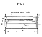
- FIG. 4 is an illustration for explaining the rotary development unit.
- the rotary development unit 3 is fixed to side plates 20 , 21 which are sheet metal.
- the development cartridges 31 through 34 placed in the rotary frame 30 .
- Each memory IC-integrated connector 40 is fixed to the end of each development cartridge 31 - 34 .
- the side plate 21 is a driven side and the side plate 20 is a non-driven side.
- the memory IC-integrated connector 40 is fixed to a connector cover 39 received in a receiving portion 22 which is formed by drawing the side plate 20 of the non-driven side.
- the receiving portion 22 surrounds the connector 40 except a surface facing the body-side connector 50 and thus functions as a shield for preventing the connector 40 from being affected by voltage applied to the development roller.
- the memory IC-integrated connector 40 is covered by a connector cover 39 and an IC protective member 38 composed of a resin ring is arranged on the inner surface of the receiving portion so as to prevent the memory IC from being affected by static electricity from the sheet metal forming the receiving portion.
- FIGS. 5 ( a )- 5 ( c ) are illustrations for explaining the memory IC-integrated connector of the embodiment, wherein FIG. 5 ( a ) is a plan view thereof, FIG. 5 ( b ) is a front view thereof, and FIG. 5 ( c ) is a sectional view taken along a line A—A of FIG. 5 ( a ).
- the memory IC-integrated connector 40 comprises a base 41 as a member for receiving impact produced during connection, and two guide members 42 which are disposed to stand on one surface (surface to be connected to the body-side connector) of the base 41 at both end portions near edges of the base 41 .
- a contact protecting member 45 Disposed on the other surface (back surface) of the base 41 is a contact protecting member 45 encompassing a memory IC substrate 46 .
- the base 41 , the guide members 42 , and the memory IC substrate 46 are integrally formed as a chassis 47 .
- contact members 43 , 44 are disposed integrally with the guide members 42 at locations between the guide members 42 to stand in parallel with the guide members 42 , respectively.
- the reason why the guide members 42 are arranged outside the contact members is that the guide members 42 of the connector 40 is encompassed by the body-side connector so as to improve the stability of connection between the connector 40 and the body-side connector during the connecting operation and to stabilize the contact state of contacts.
- contact members 43 are aligned in a line at the front side (far from the end of the development roller) and three contact members 44 are aligned in a line at the rear side (near the end of the development roller) of the chassis 47 , that is, the contact members are aligned in two lines and thus being compact as a whole.
- the contact members are not limited to be aligned in two lines and may be aligned in a line or three lines.
- the terminals of the four contact members 43 at the front side are a data terminal, a connection detecting terminal, a ground (GND) terminal, and a data reading/writing terminal, while the terminals of the three contact members 44 at the rear side are a clock terminal, a power source terminal, and a chip select (CS) terminal.
- the contact members 43 , 44 comprise contact terminals 43 a, 44 a to which terminals of the body-side connector are connected by sliding contact each other.
- the contact members 43 , 44 have spring contact terminals 43 b, 44 b extending through through holes formed in the base 41 to the back side of the base 41 .
- the spring contact terminals 43 b, 44 b are arranged to come in elastically contact with terminals of the memory IC substrate 46 .
- the spring contact terminals 43 b, 44 b come in elastically contact with the terminals of the memory IC substrate 46 .
- the memory IC substrate 46 is pressed against a mounting surface of the contact protecting member 45 by spring force of the contact terminals 43 b, 44 b so that the memory IC substrate 46 is spaced apart from the base 41 .
- the terminals 43 a, 44 a of the contact members 43 , 44 are slid to and come in contact with the terminals of the body-side connector and the impact produced by the contact is received by the base 41 .
- the impact is not directly transmitted to the contact portions between the terminals of the memory IC substrate 46 and the contacts 43 b, 44 b.
- the connector 40 is structured to have the sliding contacts to be connected to the body-side connector on one side of the base 41 as impact receiving member and the fixed contacts to be connected to the memory IC substrate supported by floating construction to have a space relative to the back side of the base 41 . Therefore, the impact, produced when the body-side connector is connected, is received by the base 41 and is not transmitted to the memory IC substrate, thereby keeping the stable contacts relative to the memory IC substrate.
- the double-contact structure composed of the contacts relative to the memory IC substrate and the contacts relative to the body-side connector achieves the arrangement of preventing the impact, produced when the body-side connector is connected, from being directly transmitted to the memory IC substrate so as to stabilize the contacts relative to the memory IC substrate, and achieves the contacts relative to the body-side connector while sliding the terminals so as to refresh the contacts, improving the reliability of the contacts.
- the connection relative to the body-side connector is conducted by the guiding portion, the impact produced during the connection is received by the impact receiving portion, and the memory IC substrate is encompassed by the contact protecting member (portion), thereby ensuring the stability of the contacts.
- the terminals relative to the body-side connector are slid to the corresponding terminals, the contacts thereof can be refreshed, thereby improving the reliability. Since the guide portion is arranged outside the terminals of the contacts relative to the connector, the insertion is stabilized, thereby ensuring the stability of the contacts of the terminals.
- the contacts of the memory IC substrate are located not to be directly exposed to outside.
- the memory IC substrate is surrounded by the contact protecting member 45 and is supported by the spring contacts inside the contact protecting member 45 .
- the four contact members aligned with the guide members 42 in a line are located at a far side relative to the development roller (at the front side) and the balance i.e. the three contact members are located at the development roller side.
- the contact member 43 G as a ground terminal is the longest so that the contact member 43 G first touches the body-side connector during the connection.
- the ground terminal 43 G is arranged at farthest from the development roller. Of cause, long terminals other than the ground terminal are preferably located outside.
- FIGS. 7 ( a ), 7 ( b ) are illustrations for explaining the installation of the memory IC substrate into the connector body.
- FIG. 7 ( a ) is an illustration showing the installed state of the memory IC substrate as seen from the back side of the connector.
- the memory IC substrate 46 is provided at a position slightly off the center thereof with a cutout 46 a.
- the front ends on the both sides of the cutout 46 a have different extension length.
- the connector body is formed with a positioning mount portion 60 having depressions of which depths are different corresponding to the both sides of the substrate. Therefore, when a user tries to insert the front ends of the substrate into the positioning mount portion 60 in the wrong way, the insertion should be unworkable. That is, the arrangement can prevent the mistaken insertion.
- the rear end of the substrate is arranged to engage a hook portion 61 of the connector body.
- FIG. 7 ( b ) is a sectional view for explaining the installation of the memory IC substrate.
- the memory IC substrate 46 is made of elastic resin.
- the front ends of the substrate are inserted into the positioning mount portion 60 .
- the substrate is pressed against the connector body by the pivotal movement and is warped by utilizing its elasticity so that the rear end of the substrate engages the hook portion 61 .
- the terminals of the memory IC substrate are in elastic contact with the spring contact terminals 43 b, 44 b, so that the memory IC substrate is pressed against the positioning mount portion 60 and the hook portion 61 because of the spring force of the contacts, thereby stabilizing the installation and stabilizing the contact state. Therefore, the inferior setting due to external force or the like may never be cause, thereby achieving the simplification of the terminal structure and thus improving the reliability of contacts.
- the memory IC substrate is made of a material having elasticity, the memory IC substrate is elastically and detachably installed to the connector body, thereby improving the assembility and applying reusability to the memory IC substrate. Since the terminals are aligned in a plurality of lines, smaller connector can be achieved. In addition, since the cutout for positioning is formed in the memory IC substrate, mistake insertion of the substrate can be prevented.
- the IC itself should be heated for unsoldering during the operation removing the memory IC so that information stored in the memory may be broken.
- terminals must be brought in contact with the memory IC attached to a narrow space of a large apparatus such as an electrophotographic apparatus which is larger than inkjet printers. This operation is extremely complex.
- the memory IC since the spring contact members make contact relative to the terminals of the memory IC substrate, the memory IC is detachable. Even though the connector body is fixed, the memory IC can be easily removed and collected so that information stored therein can be read out and reused.
- FIG. 8 is a sectional view showing the main parts of the connector into which the memory IC substrate is installed.
- the contact members 43 , 44 are formed on both sides of the chassis 47 of the connector 40 and extend over the back side of the connector body. The extending portions of the contact members 43 , 44 are bent to obtain elasticity so as to form contacts 43 b, 44 b, respectively.
- the connector body is provided with the positioning mount portion 60 and the hook portion 61 as mentioned above. As mentioned above, the end of the memory IC substrate 46 with the cutout is inserted into depressions of the positioning mount portion 60 and the substrate 46 is pressed against the connector body so that the other end engages the hook portion 61 , that is, the installation is carried out by utilizing the elasticity of the substrate. During this, the terminals, 63 , 64 of the memory IC substrate come in contact with the contacts 43 b, 44 b of the connector side to form fixed contacts.
- the terminals of the memory IC substrate are terminals 63 , 64 in two lines at the positioning mount portion 60 side relative to the center thereof.
- the spring supporting points P 1 , P 2 are located near the hook portion 61 .
- the terminals 63 , 64 come in softly contact with the contacts 43 b, 44 b by the spring force during the installation of the memory IC substrate, thereby obtaining suitable contacting force.
- the length from the spring supporting point to the contact 43 b is longer than the length from the spring supporting point to the contact 44 b. Accordingly, the force of the contacts 43 b is smaller than the force of the contact 44 b because these are made of the same material.
- the installation of the memory IC substrate is carried out by inserting the end near the terminals 63 , 64 into the depressions of the positioning mount portion 60 and pressing the substrate to force the other end to engage the hook portion as shown in FIG. 8 . Therefore, the force of the contact 43 b, which first comes into contact, is set to be smaller than that of the contact 44 b, thereby facilitating the installation and stabilizing the installation. Because the installation can be done with weak force, the memory IC substrate is hardly damaged and is therefore reuseable.
- the contact member 43 is composed of four contacts and the contact member 44 is composed of three contacts.
- the contacts are aligned in a plurality of lines (two in this embodiment) and the lines are different from each other in the number of contacts as mentioned above, the contacts of the larger number side (the contact 43 b with lower spring load) are positioned at the positioning mount portion side, thereby minimizing the force required for installation, facilitating the installation, and stabilizing the installation.
- the installation can be done with weak force, the memory IC substrate is hardly damaged and is therefore reuseable.
- the number of the contacts with lower spring load is different from the number of the contacts with higher spring load
- the number of the contacts with lower spring load is set to be larger. Even with larger number of contacts, no problem occurs because of the lower spring load. Since the force at the contact is determined by spring pressure, the terminal is not affected even with larger number of contacts.
- the contact 44 b with higher spring load and having relatively larger contact force is positioned near the center of the memory IC substrate, thereby increasing the spring contact pressure at the center when the memory IC substrate is installed. Because the spring contact pressure at the center is increased, the substrate is pressed from the center thereof so that pressure is equally applied to the positioning mount portion side and the hook portion side, thereby achieving the stable mounting. The mounted state of the substrate is stabilized.
- terminals are arranged in a plurality of lines which are different in spring load by setting the spring load of contacts at the center of the substrate to be higher than that of the other contacts of the other portion, pressure is equally applied to the positioning mount portion side and the hook portion side, thereby offering advantages of stabilizing the mounted state of the substrate.
Abstract
A connector with a built-in memory IC which is mounted on a rotary development unit of a printer. The memory IC substrate is disposed within a contact protecting member and behind the rear side of an impact receiving member. A first electric contact is disposed on the front side of the impact receiving member and is connected to a second electric contact via a conductive member. The second electric contact spring contacts the memory IC substrate. The connector contains guide members to help stabilize the connection between the connector and the body side connector of the printer.
Description
The present invention relates to a connector with a built-in memory IC for reading/writing data such as consumption of toner, to a development cartridge having such a connector, and to an image forming apparatus using such a development cartridge.
In image forming apparatuses such as printers, a memory IC is mounted on a development cartridge. By connecting the memory IC to an apparatus body-side connector, data such as information about remaining amounts of respective color toners, cartridge freshness information about whether the present cartridge is new or old, cartridge placing information for informing the apparatus body whether a cartridge is placed or not, conditions about image formation such as development bias, and recycle information about how many times a cartridge is exchanged, are written. When the development cartridge is placed, the history information is read out from the memory IC so that the information can be recognized on the apparatus body side.
In this case, for example in a cartridge of an inkjet printer, a memory IC substrate in which history information is written is connected to a connector by crimping electric wires or a memory IC substrate is soldered to terminals of a connector.
Conventionally, a memory IC to be mounted to a development cartridge comes in contact with an apparatus body-side connector so that mechanical force is directly applied to the memory IC when data is read/written. Therefore, the life of contacts of the memory IC is short. In addition, since high voltage is applied to the development roller, contact members are susceptible to field noise due to the effect of the applied voltage so that malfunction easily occurs due to static electricity and/or toner stains. Therefore, the protection of the memory IC and the stability of contacts are not enough ensured.
In case that the terminals of memory IC substrate are connected to the connector by crimping electric wires, inferior contact such as insufficient crimping and breakage of the wires may occur. In case that the memory IC substrate is soldered to the terminals of the connector, inferior contact may be occur due to bad soldering and there is another problem that when the memory IC substrate is reused, the memory IC substrate should be removed by heating so that even if it can be removed, information stored in the memory IC may be broken due to heat. Longer contact member is particularly susceptible to field noise because it serves as an antenna.
It is an object of the present invention to ensure the stability of contacts of a connector with a built-in memory IC and thus to improve the reliability.
It is another object of the present invention to ensure the stability of contacts of a connector with a built-in memory IC and thus to improve the reliability.
It is another object of the present invention to ensure the stability of contacts by avoiding the occurrence of inferior contact, and to make a memory IC substrate detachable so that the memory IC is reusable.
It is still another object of the present invention to make a memory IC substrate detachable and also stabilize the mounted state of the memory IC substrate.
Therefore, the first invention is a connector with a built-in memory IC which is mounted in a rotary development unit and of which data is read and written by bringing an apparatus body-side connector to be connected with and spaced apart form said connector, and comprises an impact receiving member; a first electric contact which is disposed on the front side of the impact receiving member; a memory IC substrate which is disposed on and apart from the rear side of the impact receiving member; and a second electric contact which is configured by bringing a conductive member extending from the first electric contact into contact with a terminal of the memory IC substrate.
The second invention is a connector with a built-in memory IC which is mounted in a rotary development unit and of which data is read and written by bringing an apparatus body-side connector to be connected with and spaced apart form said connector, and comprises a plurality of contact members; a guide member(s) which is formed with the contact members; an impact receiving member being provided on one surface thereof with said guide member; and a contact protecting member which is disposed on the other surface of the impact receiving member and encompasses a memory IC substrate.
The third invention is a connector to which a memory IC substrate is detachably attached and which comprises conductive members having connecting terminals relative to an apparatus body-side connector and connecting terminals relative to the memory IC substrate, wherein the connecting terminals of said conductive members relative to the memory IC substrate have elasticity.
The fourth invention is a connector comprising a positioning mount portion which is engaged with a front end of a memory IC substrate and a hook portion for engaging a rear end of the memory IC substrate and having contacts which are in contact with terminals of the memory IC substrate by spring force in the state that the memory IC substrate is detachably installed to the connector, wherein said contacts are aligned in a plurality of lines and, among said contacts, a contact at the center side of a substrate is set to have a spring load higher than the other contacts.
FIGS. 2(a)-2(c) are illustrations for explaining the position for the replacement of a development cartridge, the position for reading/writing data of a memory IC, and the position for development standby, respectively,
FIGS. 3(a), 3(b) are illustrations for connection and separation between connectors for a memory IC,
FIGS. 5(a)-5(c) are illustrations for explaining a connector with a built-in memory IC,
FIGS. 7(a), 7(b) are illustrations for explaining the installation of a memory IC substrate into a connector body, and
Hereinafter, an embodiment of the present invention will be described with reference to the attached drawings.
On the other hand, a paper sheet taken from a sheet cassette 6 is fed through a feeding passage 7 to a secondary transfer position between the transfer belt driving roller 5 and a transfer roller 8 where the four toner images are transferred to the paper sheet at once. Here, the top of the image on the transfer belt 4 is detected by a belt position detection sensor 9. The control is conducted so that the top of the image and the top of the paper sheet are met. The image secondarily transferred to the paper sheet is fixed by a fixing unit 10. In case of double-side printing, the paper sheet is returned to the feeding passage 7 and an image is transferred to the verso of the paper sheet. After transferred and fixed, the paper sheet is discharged outside the apparatus.
Each of the development cartridges 31 through 34 for four colors of the rotary development unit 3 has a connector 40 with a built-in memory IC (hereinafter, sometimes referred to as “memory IC-integrated connector”) (as will be described later in detail) mounted therein. According to this structure, a body-side connector 50 can read/write data. The body-side connector 50 is driven by a driving member 51 with a motor to move ahead to its advance position and moves astern to its resting position. When the cartridge is replaced with new one, the body-side connector 50 moves ahead to the advance position where the body-side connector 50 is electrically connected to the connector 40 to read/write the data of the memory IC. Normally, the body-side connector 50 is in the resting position. Each development cartridge can be removed and attached to the apparatus at a position corresponding to a cartridge-replacement opening 11 formed in the apparatus body. The image forming apparatus is provided with an exhaust duct 12. Scattered toner particles and other dust are sucked through a suction port 14 near a development nip where the development roller and the photoreceptor are in contact. After filtered by a filter 13, the sucked air is exhausted through the exhaust duct 12. In this case, the position where the memory IC-integrated connector 40 and the body-side connector 50 are connected is arranged on the upstream side than the development nip in the rotational direction of the development unit, thereby preventing the connecting portion between the connectors from being affected by scattered toner particles.
FIGS. 2(a)-2(c) are illustrations for explaining the position for the replacement of the development cartridge, the position for reading/writing data of the memory IC, and the position for development standby. The home position of the rotary development unit is detected by a position detecting plate 37 and a position detecting sensor 36 wherein the position detecting sensor 36 senses a cutout position of the position detecting plate 37.
FIG. 2(a) is an illustration for explaining the cartridge replacement position (Position {circle around (1)}). As mentioned above, the cartridge-replacement opening 11 is formed in the apparatus body. The development rollers {circle around (1)} through {circle around (4)} of the rotary development unit 3 can be replaced at the position corresponding to the cartridge-replacement opening 11. In this position {circle around (1)}, any of the connectors 40 of the development cartridges does not face the body-side connector 50 and the photoreceptor 1 does not face any of development roller.
FIG. 2(b) shows the position where data is read/written from/to the memory IC and the development roller faces the photoreceptor so as to conduct development (Position {circle around (2)}). As a reading/writing command is outputted from the apparatus body side, the positional relation of Position {circle around (2)} is satisfied and the body-side connector 50 is activated to connect the connector 40, thereby reading/writing data.
FIG. 2(c) shows a position on the way of switching the development operation by the rotary development unit from one color to another color (Position {circle around (3)}). In this position, the photoreceptor and any development roller do not face each other.
FIGS. 3(a), 3(b) are illustrations for connection and separation between the connectors.
As shown in FIG. 3(a), for connection, the body-side connector 50 is moved ahead to the advance position by a motor. As will be described later, the body-side connector 50 is guided by guiding members of the memory IC-integrated connector 40 and is therefore plugged with the memory IC-integrated connector 40. The connectors are electrically connected by sliding contact between terminals thereof. For separation, the connector 50 is moved astern to the resting position so that the connectors 40 and 50 are separated. The connector 40 is fixed to the development unit by connector-fixing screws 48 and the connector 50 is fixed to the apparatus body by connector-fixing pins 53.
The rotary development unit 3 is fixed to side plates 20, 21 which are sheet metal. The development cartridges 31 through 34 placed in the rotary frame 30. Each memory IC-integrated connector 40 is fixed to the end of each development cartridge 31-34. In this embodiment, the side plate 21 is a driven side and the side plate 20 is a non-driven side. To prevent the memory IC-integrated connector 40 from being affected by heat of the driving means, the memory IC-integrated connector 40 is fixed to a connector cover 39 received in a receiving portion 22 which is formed by drawing the side plate 20 of the non-driven side. The receiving portion 22 surrounds the connector 40 except a surface facing the body-side connector 50 and thus functions as a shield for preventing the connector 40 from being affected by voltage applied to the development roller. The memory IC-integrated connector 40 is covered by a connector cover 39 and an IC protective member 38 composed of a resin ring is arranged on the inner surface of the receiving portion so as to prevent the memory IC from being affected by static electricity from the sheet metal forming the receiving portion.
FIGS. 5(a)-5(c) are illustrations for explaining the memory IC-integrated connector of the embodiment, wherein FIG. 5(a) is a plan view thereof, FIG. 5(b) is a front view thereof, and FIG. 5(c) is a sectional view taken along a line A—A of FIG. 5(a). The memory IC-integrated connector 40 comprises a base 41 as a member for receiving impact produced during connection, and two guide members 42 which are disposed to stand on one surface (surface to be connected to the body-side connector) of the base 41 at both end portions near edges of the base 41. Disposed on the other surface (back surface) of the base 41 is a contact protecting member 45 encompassing a memory IC substrate 46. The base 41, the guide members 42, and the memory IC substrate 46 are integrally formed as a chassis 47. In addition, contact members 43, 44 are disposed integrally with the guide members 42 at locations between the guide members 42 to stand in parallel with the guide members 42, respectively. The reason why the guide members 42 are arranged outside the contact members is that the guide members 42 of the connector 40 is encompassed by the body-side connector so as to improve the stability of connection between the connector 40 and the body-side connector during the connecting operation and to stabilize the contact state of contacts.
In this embodiment, four contact members 43 are aligned in a line at the front side (far from the end of the development roller) and three contact members 44 are aligned in a line at the rear side (near the end of the development roller) of the chassis 47, that is, the contact members are aligned in two lines and thus being compact as a whole. Of cause, the contact members are not limited to be aligned in two lines and may be aligned in a line or three lines. The terminals of the four contact members 43 at the front side are a data terminal, a connection detecting terminal, a ground (GND) terminal, and a data reading/writing terminal, while the terminals of the three contact members 44 at the rear side are a clock terminal, a power source terminal, and a chip select (CS) terminal.
The contact members 43, 44 comprise contact terminals 43 a, 44 a to which terminals of the body-side connector are connected by sliding contact each other. The contact members 43, 44 have spring contact terminals 43 b, 44 b extending through through holes formed in the base 41 to the back side of the base 41. The spring contact terminals 43 b, 44 b are arranged to come in elastically contact with terminals of the memory IC substrate 46. When the memory IC substrate 46 is mounted to the contact protecting member 45, the spring contact terminals 43 b, 44 b come in elastically contact with the terminals of the memory IC substrate 46. The memory IC substrate 46 is pressed against a mounting surface of the contact protecting member 45 by spring force of the contact terminals 43 b, 44 b so that the memory IC substrate 46 is spaced apart from the base 41. When the body-side connector 50 is driven by the motor to move ahead to its advance position and thus come in contact with the connector 40, the terminals 43 a, 44 a of the contact members 43, 44 are slid to and come in contact with the terminals of the body-side connector and the impact produced by the contact is received by the base 41. However, since the memory IC substrate 46 is spaced apart from the base 41, the impact is not directly transmitted to the contact portions between the terminals of the memory IC substrate 46 and the contacts 43 b, 44 b.
The connector 40 is structured to have the sliding contacts to be connected to the body-side connector on one side of the base 41 as impact receiving member and the fixed contacts to be connected to the memory IC substrate supported by floating construction to have a space relative to the back side of the base 41. Therefore, the impact, produced when the body-side connector is connected, is received by the base 41 and is not transmitted to the memory IC substrate, thereby keeping the stable contacts relative to the memory IC substrate.
The double-contact structure composed of the contacts relative to the memory IC substrate and the contacts relative to the body-side connector achieves the arrangement of preventing the impact, produced when the body-side connector is connected, from being directly transmitted to the memory IC substrate so as to stabilize the contacts relative to the memory IC substrate, and achieves the contacts relative to the body-side connector while sliding the terminals so as to refresh the contacts, improving the reliability of the contacts.
Because of the triple structure composed of a guiding portion, an impact receiving portion, and a contact protecting portion, the connection relative to the body-side connector is conducted by the guiding portion, the impact produced during the connection is received by the impact receiving portion, and the memory IC substrate is encompassed by the contact protecting member (portion), thereby ensuring the stability of the contacts. In addition, since the terminals relative to the body-side connector are slid to the corresponding terminals, the contacts thereof can be refreshed, thereby improving the reliability. Since the guide portion is arranged outside the terminals of the contacts relative to the connector, the insertion is stabilized, thereby ensuring the stability of the contacts of the terminals.
In order to protect the memory IC substrate to be mounted to the connector from inferior contact due to toner stains and from destruction of data due to effect of static electricity, it is preferable that the contacts of the memory IC substrate are located not to be directly exposed to outside. In this embodiment, the memory IC substrate is surrounded by the contact protecting member 45 and is supported by the spring contacts inside the contact protecting member 45.
Among the seven contact members shown in FIG. 5 , the four contact members aligned with the guide members 42 in a line are located at a far side relative to the development roller (at the front side) and the balance i.e. the three contact members are located at the development roller side. Among the four contact members at the front side, the contact member 43G as a ground terminal is the longest so that the contact member 43G first touches the body-side connector during the connection.
At the time of development, a voltage of 2 KVp-p is applied to the development roller. The contact members are susceptible to field noise due to the effect of the applied voltage. The longest contact member is particularly susceptible to field noise because it serves as an antenna. Accordingly, in this embodiment, the ground terminal 43G is arranged at farthest from the development roller. Of cause, long terminals other than the ground terminal are preferably located outside.
FIGS. 7(a), 7(b) are illustrations for explaining the installation of the memory IC substrate into the connector body.
FIG. 7(a) is an illustration showing the installed state of the memory IC substrate as seen from the back side of the connector. The memory IC substrate 46 is provided at a position slightly off the center thereof with a cutout 46 a. The front ends on the both sides of the cutout 46 a have different extension length. The connector body is formed with a positioning mount portion 60 having depressions of which depths are different corresponding to the both sides of the substrate. Therefore, when a user tries to insert the front ends of the substrate into the positioning mount portion 60 in the wrong way, the insertion should be unworkable. That is, the arrangement can prevent the mistaken insertion. On the other hand, the rear end of the substrate is arranged to engage a hook portion 61 of the connector body.
FIG. 7(b) is a sectional view for explaining the installation of the memory IC substrate. The memory IC substrate 46 is made of elastic resin. The front ends of the substrate are inserted into the positioning mount portion 60. The substrate is pressed against the connector body by the pivotal movement and is warped by utilizing its elasticity so that the rear end of the substrate engages the hook portion 61. At this point, the terminals of the memory IC substrate are in elastic contact with the spring contact terminals 43 b, 44 b, so that the memory IC substrate is pressed against the positioning mount portion 60 and the hook portion 61 because of the spring force of the contacts, thereby stabilizing the installation and stabilizing the contact state. Therefore, the inferior setting due to external force or the like may never be cause, thereby achieving the simplification of the terminal structure and thus improving the reliability of contacts.
Further, since the memory IC substrate is made of a material having elasticity, the memory IC substrate is elastically and detachably installed to the connector body, thereby improving the assembility and applying reusability to the memory IC substrate. Since the terminals are aligned in a plurality of lines, smaller connector can be achieved. In addition, since the cutout for positioning is formed in the memory IC substrate, mistake insertion of the substrate can be prevented.
For reusing the memory IC substrate, in case that the memory IC substrate is fixed by soldering or the like such as in an inkjet printer, the IC itself should be heated for unsoldering during the operation removing the memory IC so that information stored in the memory may be broken. On the other hand, for reading out information stored in the memory without detaching the memory IC, terminals must be brought in contact with the memory IC attached to a narrow space of a large apparatus such as an electrophotographic apparatus which is larger than inkjet printers. This operation is extremely complex.
In this embodiment, however, since the spring contact members make contact relative to the terminals of the memory IC substrate, the memory IC is detachable. Even though the connector body is fixed, the memory IC can be easily removed and collected so that information stored therein can be read out and reused.
The contact members 43, 44 are formed on both sides of the chassis 47 of the connector 40 and extend over the back side of the connector body. The extending portions of the contact members 43, 44 are bent to obtain elasticity so as to form contacts 43 b, 44 b, respectively. The connector body is provided with the positioning mount portion 60 and the hook portion 61 as mentioned above. As mentioned above, the end of the memory IC substrate 46 with the cutout is inserted into depressions of the positioning mount portion 60 and the substrate 46 is pressed against the connector body so that the other end engages the hook portion 61, that is, the installation is carried out by utilizing the elasticity of the substrate. During this, the terminals, 63, 64 of the memory IC substrate come in contact with the contacts 43 b, 44 b of the connector side to form fixed contacts.
In this embodiment, the terminals of the memory IC substrate are terminals 63, 64 in two lines at the positioning mount portion 60 side relative to the center thereof. For locating the spring supporting points P1, P2 farthest from the terminals 63, 64, the spring supporting points P1, P2 are located near the hook portion 61. According to this structure, the terminals 63, 64 come in softly contact with the contacts 43 b, 44 b by the spring force during the installation of the memory IC substrate, thereby obtaining suitable contacting force.
Since the spring supporting points P1, P2 are located at substantially the same position, the length from the spring supporting point to the contact 43 b is longer than the length from the spring supporting point to the contact 44 b. Accordingly, the force of the contacts 43 b is smaller than the force of the contact 44 b because these are made of the same material. The installation of the memory IC substrate is carried out by inserting the end near the terminals 63, 64 into the depressions of the positioning mount portion 60 and pressing the substrate to force the other end to engage the hook portion as shown in FIG. 8. Therefore, the force of the contact 43 b, which first comes into contact, is set to be smaller than that of the contact 44 b, thereby facilitating the installation and stabilizing the installation. Because the installation can be done with weak force, the memory IC substrate is hardly damaged and is therefore reuseable.
As described above with regard to FIG. 5 , the contact member 43 is composed of four contacts and the contact member 44 is composed of three contacts. In case of that the contacts are aligned in a plurality of lines (two in this embodiment) and the lines are different from each other in the number of contacts as mentioned above, the contacts of the larger number side (the contact 43 b with lower spring load) are positioned at the positioning mount portion side, thereby minimizing the force required for installation, facilitating the installation, and stabilizing the installation. In addition, because the installation can be done with weak force, the memory IC substrate is hardly damaged and is therefore reuseable.
In case that the number of the contacts with lower spring load is different from the number of the contacts with higher spring load, the number of the contacts with lower spring load is set to be larger. Even with larger number of contacts, no problem occurs because of the lower spring load. Since the force at the contact is determined by spring pressure, the terminal is not affected even with larger number of contacts.
When the contacts of the larger number side (the contact 43 b with lower spring load) are positioned on the positioning mount portion side, the contact 44 b with higher spring load and having relatively larger contact force is positioned near the center of the memory IC substrate, thereby increasing the spring contact pressure at the center when the memory IC substrate is installed. Because the spring contact pressure at the center is increased, the substrate is pressed from the center thereof so that pressure is equally applied to the positioning mount portion side and the hook portion side, thereby achieving the stable mounting. The mounted state of the substrate is stabilized.
As mentioned above, in case that terminals are arranged in a plurality of lines which are different in spring load by setting the spring load of contacts at the center of the substrate to be higher than that of the other contacts of the other portion, pressure is equally applied to the positioning mount portion side and the hook portion side, thereby offering advantages of stabilizing the mounted state of the substrate.
Claims (12)
1. A connector with a built-in memory IC which is mounted in a rotary development unit and of which data is read and written by bringing an apparatus body-side connector in contact with said connector, comprising: a plurality of contact members; a guide member(s) which is formed integrally with the contact members for guiding the movement of the apparatus body-side connector; an impact receiving member being provided on one surface thereof with said guide member; and a contact protecting member which is disposed on the other surface of the impact receiving member and encompasses a memory IC substrate.
2. A connector as claimed in claim 1 , wherein said guide member is formed outside of the contact members.
3. A connector as claimed in claim 1 , wherein said contact members have contacts of which electric connect is achieved by sliding with terminals of the apparatus body-side connector, and wherein conductive members extending from said contact members through the impact receiving member are elastically in contact with terminals of the memory IC substrate by spring force so as to form fixed contacts.
4. A development cartridge having a connector, as claimed in claim 1 , 2, or 3, which is fixed to an end thereof.
5. An image forming apparatus having a development cartridge as claimed in claim 4 .
6. A connector to which a memory IC substrate is detachably attached and which comprises conductive members having connecting terminal relative to an apparatus body-side connector and connecting terminals relative to the memory IC substrate, wherein the connecting terminals of said conductive members relative to the memory IC substrate have elasticity,
wherein the front end of said memory IC substrate is inserted into a mount portion of the connector body and the rear end of said memory IC substrate engages a hook portion of the connector body by utilizing the elasticity of the memory IC substrate, thereby installing the memory IC substrate to the connector body.
7. A connector as claimed in claim 6 , wherein said memory IC substrate has a cutout which is formed in the front end thereof to be inserted into the mount portion of the connector body at a position slightly off the center thereof.
8. A connector as claimed in claim 6 or 7 , wherein the line of the connecting terminals of a plurality of current carrying elements relative to the memory IC substrate is aligned with the line of the terminals of the memory IC substrate.
9. A connector comprising a positioning mount portion which is engaged with a front end of a memory IC substrate and a hook portion for engaging a rear end of the memory IC substrate and having contacts which are in contact with terminals of the memory IC substrate by spring force in the state that the memory IC substrate is detachably installed to the connector, wherein said contacts are aligned in a plurality of lines and, among said contacts, a contact at the center side of a substrate is set to have a spring load higher than the other contacts.
10. A connector as claimed in claim 9 , wherein said contacts are aligned in two lines, the contacts in the first line have lower spring load and are located at the positioning mount portion side, and the contacts in the second line have higher spring load and are located at the center side of the substrate.
11. A development cartridge having a connector, as claimed in claim 9 or 10 , which is fixed to an end thereof.
12. An image forming apparatus having a development cartridge as claimed in claim 11 .
Applications Claiming Priority (8)
| Application Number | Priority Date | Filing Date | Title |
|---|---|---|---|
| JP2002-041139 | 2002-02-19 | ||
| JP2002-041140 | 2002-02-19 | ||
| JP2002041140A JP2003241463A (en) | 2002-02-19 | 2002-02-19 | Connector, developing cartridge and image forming apparatus |
| JP2002041139A JP2003241462A (en) | 2002-02-19 | 2002-02-19 | Connector, developing cartridge and image forming apparatus |
| JP2002-042877 | 2002-02-20 | ||
| JP2002042877A JP2003243104A (en) | 2002-02-20 | 2002-02-20 | Connector, development cartridge and image forming device |
| JP2002-057178 | 2002-03-04 | ||
| JP2002057178A JP2003257530A (en) | 2002-03-04 | 2002-03-04 | Connector, developer cartridge and image forming device |
Publications (2)
| Publication Number | Publication Date |
|---|---|
| US20030170042A1 US20030170042A1 (en) | 2003-09-11 |
| US6892039B2 true US6892039B2 (en) | 2005-05-10 |
Family
ID=27670918
Family Applications (1)
| Application Number | Title | Priority Date | Filing Date |
|---|---|---|---|
| US10/367,968 Expired - Fee Related US6892039B2 (en) | 2002-02-19 | 2003-02-19 | Connector having a built-in memory IC mounted on a development cartridge |
Country Status (5)
| Country | Link |
|---|---|
| US (1) | US6892039B2 (en) |
| EP (3) | EP1691455A1 (en) |
| CN (2) | CN1249537C (en) |
| AT (1) | ATE391944T1 (en) |
| DE (1) | DE60320163T2 (en) |
Cited By (6)
| Publication number | Priority date | Publication date | Assignee | Title |
|---|---|---|---|---|
| US20040223772A1 (en) * | 2003-03-20 | 2004-11-11 | Seiko Epson Corporation | Image forming apparatus and a storage controlling method for information on an improper detachment of developer cartridge to be written in a cartridge storage means |
| US20100189460A1 (en) * | 2009-01-23 | 2010-07-29 | Samsung Electronics Co., Ltd. | Image forming apparatus |
| US20120301173A1 (en) * | 2008-04-01 | 2012-11-29 | Yoon Seop Eom | Image forming apparatus and control method thereof |
| US9606498B2 (en) * | 2015-02-19 | 2017-03-28 | Fuji Xerox Co., Ltd. | Electronic-component attachment structure, attachable-detachable unit, and image forming apparatus |
| USRE46519E1 (en) * | 2007-09-11 | 2017-08-22 | S-Printing Solution Co., Ltd. | Developing device, memory unit thereof, and image forming apparatus |
| US11046602B2 (en) | 2015-09-17 | 2021-06-29 | Charles E. C. Harris | Fluid purification apparatus and method |
Families Citing this family (19)
| Publication number | Priority date | Publication date | Assignee | Title |
|---|---|---|---|---|
| KR100727943B1 (en) * | 2005-06-27 | 2007-06-14 | 삼성전자주식회사 | Toner cartridge having the life detection board built-in and electrophotographic image forming apparatus using the same |
| JP4946425B2 (en) * | 2006-12-26 | 2012-06-06 | セイコーエプソン株式会社 | Liquid container |
| US7840154B2 (en) * | 2007-02-20 | 2010-11-23 | Brother Kogyo Kabushiki Kaisha | Image forming device and cartridge |
| JP5066716B2 (en) * | 2007-09-14 | 2012-11-07 | 株式会社リコー | Image forming apparatus |
| SG10201903208SA (en) | 2010-06-11 | 2019-05-30 | Ricoh Co Ltd | Information storage device, removable device, developer container, and image forming apparatus |
| CN102193475B (en) * | 2011-05-10 | 2012-10-24 | 珠海艾派克微电子有限公司 | Imaging box chip and imaging box |
| JP6375609B2 (en) * | 2012-10-19 | 2018-08-22 | 株式会社リコー | Detachable device and image forming apparatus |
| JP6018971B2 (en) | 2013-05-20 | 2016-11-02 | 株式会社沖データ | Substrate mounting mechanism, developer container, image forming unit, and image forming apparatus |
| CN105629691B (en) * | 2014-08-22 | 2019-11-08 | 纳思达股份有限公司 | A kind of Delevoping cartridge |
| KR20150106729A (en) | 2014-03-12 | 2015-09-22 | 삼성전자주식회사 | Cartridge and electrophotographic image forming apparatus using the same |
| EP3118001B1 (en) * | 2014-03-14 | 2020-09-02 | Seiko Epson Corporation | Recording apparatus |
| JP6269234B2 (en) * | 2014-03-26 | 2018-01-31 | セイコーエプソン株式会社 | Liquid container, adapter, and liquid ejection device |
| CN103926822A (en) * | 2014-04-30 | 2014-07-16 | 珠海天威飞马打印耗材有限公司 | Processing box |
| JP6589630B2 (en) | 2015-12-25 | 2019-10-16 | ブラザー工業株式会社 | Developer cartridge |
| JP6582972B2 (en) | 2015-12-25 | 2019-10-02 | ブラザー工業株式会社 | Developer cartridge |
| JP6512177B2 (en) * | 2016-06-08 | 2019-05-15 | 京セラドキュメントソリューションズ株式会社 | Image forming apparatus provided with toner container |
| US10725422B2 (en) * | 2018-10-25 | 2020-07-28 | Lexmark International, Inc. | Toner cartridge electrical contacts |
| JP7370905B2 (en) | 2020-03-10 | 2023-10-30 | キヤノン株式会社 | Sheet conveyance device and image forming device |
| CN113968081A (en) * | 2020-07-23 | 2022-01-25 | 杭州旗捷科技有限公司 | Circuit board and preparation method thereof, circuit device and preparation method thereof, and printing material container assembly |
Citations (10)
| Publication number | Priority date | Publication date | Assignee | Title |
|---|---|---|---|---|
| US4222622A (en) | 1978-06-12 | 1980-09-16 | Gte Products Corporation | Electrical connector for circuit board |
| US4903167A (en) | 1987-06-12 | 1990-02-20 | Schleicher For Accommodating Electric Gmbh & Co. Kg | Casing for accommodating electric and/or electronic components |
| EP0813356A1 (en) | 1996-06-11 | 1997-12-17 | Sun Microsystems, Inc. | Hold-down collar for attachment of IC substrates and elastomeric material to PCBs |
| EP0821445A1 (en) | 1996-07-24 | 1998-01-28 | Canon Kabushiki Kaisha | Electrical connector, process cartridge and electrophotographic image forming apparatus |
| EP0822469A1 (en) | 1996-07-31 | 1998-02-04 | Canon Kabushiki Kaisha | Process cartridge and image forming apparatus to which process cartridge can detachably be mounted |
| EP0913745A2 (en) | 1997-10-31 | 1999-05-06 | Canon Kabushiki Kaisha | Connector part, process cartridge and electrophotographic image forming apparatus |
| US5980294A (en) * | 1996-11-15 | 1999-11-09 | Olympus Optical Co., Ltd. | IC card loading device |
| US6014533A (en) | 1997-05-12 | 2000-01-11 | Canon Kabushiki Kaisha | Connector, processing unit or process cartridge, and electrophotographic image forming apparatus |
| US6056573A (en) * | 1996-07-30 | 2000-05-02 | Alps Electric Co., Ltd. | IC card connector |
| US6238248B1 (en) * | 1997-12-17 | 2001-05-29 | Japan Solderless Terminal Mfg. Co., Ltd. | Connector for thin cartridge |
Family Cites Families (2)
| Publication number | Priority date | Publication date | Assignee | Title |
|---|---|---|---|---|
| DE4111912C2 (en) * | 1991-04-12 | 1993-10-14 | Kloeckner Moeller Gmbh | Circuit board arrangement and contact device for control systems |
| US5697802A (en) * | 1994-12-15 | 1997-12-16 | I-Pex Co., Ltd. | Electrical connector |
-
2003
- 2003-02-19 EP EP06007194A patent/EP1691455A1/en not_active Withdrawn
- 2003-02-19 EP EP03003182A patent/EP1338931B1/en not_active Expired - Lifetime
- 2003-02-19 EP EP06007191A patent/EP1701224A1/en not_active Withdrawn
- 2003-02-19 DE DE60320163T patent/DE60320163T2/en not_active Expired - Lifetime
- 2003-02-19 CN CN03104650.9A patent/CN1249537C/en not_active Expired - Fee Related
- 2003-02-19 CN CN03204366.XU patent/CN2673642Y/en not_active Expired - Fee Related
- 2003-02-19 US US10/367,968 patent/US6892039B2/en not_active Expired - Fee Related
- 2003-02-19 AT AT03003182T patent/ATE391944T1/en not_active IP Right Cessation
Patent Citations (13)
| Publication number | Priority date | Publication date | Assignee | Title |
|---|---|---|---|---|
| US4222622A (en) | 1978-06-12 | 1980-09-16 | Gte Products Corporation | Electrical connector for circuit board |
| US4903167A (en) | 1987-06-12 | 1990-02-20 | Schleicher For Accommodating Electric Gmbh & Co. Kg | Casing for accommodating electric and/or electronic components |
| EP0813356A1 (en) | 1996-06-11 | 1997-12-17 | Sun Microsystems, Inc. | Hold-down collar for attachment of IC substrates and elastomeric material to PCBs |
| US5907748A (en) * | 1996-07-24 | 1999-05-25 | Canon Kabushiki Kaisha | Electrical connector, process cartridge and electrophotographic image forming apparatus |
| EP0821445A1 (en) | 1996-07-24 | 1998-01-28 | Canon Kabushiki Kaisha | Electrical connector, process cartridge and electrophotographic image forming apparatus |
| US6056573A (en) * | 1996-07-30 | 2000-05-02 | Alps Electric Co., Ltd. | IC card connector |
| EP0822469A1 (en) | 1996-07-31 | 1998-02-04 | Canon Kabushiki Kaisha | Process cartridge and image forming apparatus to which process cartridge can detachably be mounted |
| US5963759A (en) * | 1996-07-31 | 1999-10-05 | Canon Kabushiki Kaisha | Process cartridge and image forming apparatus to which process cartridge can detachably be mounted |
| US5980294A (en) * | 1996-11-15 | 1999-11-09 | Olympus Optical Co., Ltd. | IC card loading device |
| US6014533A (en) | 1997-05-12 | 2000-01-11 | Canon Kabushiki Kaisha | Connector, processing unit or process cartridge, and electrophotographic image forming apparatus |
| EP0913745A2 (en) | 1997-10-31 | 1999-05-06 | Canon Kabushiki Kaisha | Connector part, process cartridge and electrophotographic image forming apparatus |
| US6349182B2 (en) * | 1997-10-31 | 2002-02-19 | Canon Kabushiki Kaisha | Connector unit, process cartridge and electrophotographic image forming apparatus |
| US6238248B1 (en) * | 1997-12-17 | 2001-05-29 | Japan Solderless Terminal Mfg. Co., Ltd. | Connector for thin cartridge |
Cited By (10)
| Publication number | Priority date | Publication date | Assignee | Title |
|---|---|---|---|---|
| US20040223772A1 (en) * | 2003-03-20 | 2004-11-11 | Seiko Epson Corporation | Image forming apparatus and a storage controlling method for information on an improper detachment of developer cartridge to be written in a cartridge storage means |
| US7076179B2 (en) * | 2003-03-20 | 2006-07-11 | Seiko Epson Corporation | Image forming apparatus and a storage controlling method for information on an improper detachment of developer cartridge to be written in a cartridge storage means |
| US20060210285A1 (en) * | 2003-03-20 | 2006-09-21 | Seiko Epson Corporation | Image forming apparatus and a storage controlling method for information on an improper detachment of a developer cartridge to be written in a cartridge storage means |
| US7218869B2 (en) | 2003-03-20 | 2007-05-15 | Seiko Epson Corporation | Image forming apparatus and a storage controlling method for information on an improper detachment of a developer cartridge to be written in a cartridge storage means |
| USRE46519E1 (en) * | 2007-09-11 | 2017-08-22 | S-Printing Solution Co., Ltd. | Developing device, memory unit thereof, and image forming apparatus |
| US20120301173A1 (en) * | 2008-04-01 | 2012-11-29 | Yoon Seop Eom | Image forming apparatus and control method thereof |
| US20100189460A1 (en) * | 2009-01-23 | 2010-07-29 | Samsung Electronics Co., Ltd. | Image forming apparatus |
| US8744300B2 (en) * | 2009-01-23 | 2014-06-03 | Samsung Electronics Co., Ltd. | Image forming apparatus |
| US9606498B2 (en) * | 2015-02-19 | 2017-03-28 | Fuji Xerox Co., Ltd. | Electronic-component attachment structure, attachable-detachable unit, and image forming apparatus |
| US11046602B2 (en) | 2015-09-17 | 2021-06-29 | Charles E. C. Harris | Fluid purification apparatus and method |
Also Published As
| Publication number | Publication date |
|---|---|
| CN1249537C (en) | 2006-04-05 |
| DE60320163T2 (en) | 2009-05-20 |
| EP1338931B1 (en) | 2008-04-09 |
| CN1444113A (en) | 2003-09-24 |
| DE60320163D1 (en) | 2008-05-21 |
| EP1691455A1 (en) | 2006-08-16 |
| ATE391944T1 (en) | 2008-04-15 |
| US20030170042A1 (en) | 2003-09-11 |
| EP1701224A1 (en) | 2006-09-13 |
| CN2673642Y (en) | 2005-01-26 |
| EP1338931A1 (en) | 2003-08-27 |
Similar Documents
| Publication | Publication Date | Title |
|---|---|---|
| US6892039B2 (en) | Connector having a built-in memory IC mounted on a development cartridge | |
| RU2501660C2 (en) | Printing material container | |
| US20060219770A1 (en) | Image forming apparatus | |
| WO2017114140A1 (en) | Image forming apparatus toner cartridge, developing cartridge and image forming apparatus | |
| JP2006221010A (en) | Cartridge for image formation and image forming apparatus | |
| EP3118689B1 (en) | Electrophotographic image forming apparatus and developing device | |
| JP3969127B2 (en) | Connector, developing cartridge, and image forming apparatus | |
| JP4386616B2 (en) | Connector, developing cartridge, and image forming apparatus | |
| JP2003228210A (en) | Developing device and image forming apparatus using it | |
| JP3956105B2 (en) | Connector, developing cartridge, and image forming apparatus | |
| CN105911842A (en) | Electronic-Component Attachment Structure, Attachable-Detachable Unit, And Image Forming Apparatus | |
| JP2003243104A (en) | Connector, development cartridge and image forming device | |
| JP3962983B2 (en) | Connector, developing cartridge, and image forming apparatus | |
| JP2003241462A (en) | Connector, developing cartridge and image forming apparatus | |
| JP2003255697A (en) | Image forming apparatus | |
| JP2003255647A (en) | Image forming apparatus | |
| JP6348379B2 (en) | Image forming apparatus and detachable unit | |
| JP2003243070A (en) | Connector, cartridge for development, and image forming device | |
| JP2003241463A (en) | Connector, developing cartridge and image forming apparatus | |
| JP2003255646A (en) | Image forming apparatus | |
| JP2003257530A (en) | Connector, developer cartridge and image forming device | |
| JP2003255648A (en) | Developing cartridge and image forming apparatus | |
| JPH1063166A (en) | Image forming device | |
| JP7467948B2 (en) | Image forming device | |
| JP2003228211A (en) | Developing device and image forming apparatus using it |
Legal Events
| Date | Code | Title | Description |
|---|---|---|---|
| AS | Assignment |
Owner name: SEIKO EPSON CORPORATION, JAPAN Free format text: ASSIGNMENT OF ASSIGNORS INTEREST;ASSIGNORS:OKAMOTO, KATSUMI;SHIROKOSHI, JUNJI;AOKI, TAKESHI;REEL/FRAME:014063/0737 Effective date: 20030423 |
|
| FPAY | Fee payment |
Year of fee payment: 4 |
|
| FEPP | Fee payment procedure |
Free format text: PAYOR NUMBER ASSIGNED (ORIGINAL EVENT CODE: ASPN); ENTITY STATUS OF PATENT OWNER: LARGE ENTITY |
|
| REMI | Maintenance fee reminder mailed | ||
| LAPS | Lapse for failure to pay maintenance fees | ||
| STCH | Information on status: patent discontinuation |
Free format text: PATENT EXPIRED DUE TO NONPAYMENT OF MAINTENANCE FEES UNDER 37 CFR 1.362 |
|
| FP | Lapsed due to failure to pay maintenance fee |
Effective date: 20130510 |