以下、本発明を実施するための形態について、図面を参照して詳細に説明する。各図中、同一又は相当する部分には同一の符号を付しており、その説明は適宜に簡略化ないし省略する。
まず、画像形成装置の全体構成と動作について説明する。
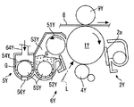
図1に示す画像形成装置は、イエロー、マゼンタ、シアン、ブラックの現像剤を用いてフルカラー画像を形成可能な複写機である。画像形成装置本体100の上方に配置されるトナー容器収容部70には、イエロー、マゼンタ、シアン、ブラックに対応した4つの着脱可能装置としてのトナー容器32Y、32M、32C、32Kが着脱可能(交換自在)に設置されている。
Hereinafter, embodiments for carrying out the present invention will be described in detail with reference to the drawings. In the drawings, the same or corresponding parts are denoted by the same reference numerals, and the description thereof is simplified or omitted as appropriate.
First, the overall configuration and operation of the image forming apparatus will be described.
The image forming apparatus shown in FIG. 1 is a copier capable of forming a full-color image using yellow, magenta, cyan, and black developers. Four toner containers 32Y, 32M, 32C, and 32K corresponding to yellow, magenta, cyan, and black are detachable (replaceable) in the toner container housing portion 70 disposed above the image forming apparatus main body 100. It is installed freely.
トナー容器収容部70の下方には、中間転写ユニット15が配設されている。中間転写ユニット15が備える中間転写ベルト8には対向するように、各色(イエロー、マゼンタ、シアン、ブラック)に対応した作像部6Y、6M、6C、6Kが並設されている。着脱可能装置としてのトナー容器32Y、32M、32C、32Kの下方には、それぞれトナー補給装置60Y、60M、60C、60Kが配設されている。トナー容器32Y、32M、32C、32Kに収容された現像剤となるトナーは、それぞれトナー補給装置60Y、60M、60C、60Kによって、作像部6Y、6M、6C、6Kの現像装置内に供給(補給)される。
An intermediate transfer unit 15 is disposed below the toner container housing portion 70. Image forming portions 6Y, 6M, 6C, and 6K corresponding to the respective colors (yellow, magenta, cyan, and black) are arranged in parallel so as to face the intermediate transfer belt 8 provided in the intermediate transfer unit 15. Below the toner containers 32Y, 32M, 32C, and 32K as detachable devices, toner replenishing devices 60Y, 60M, 60C, and 60K are disposed, respectively. The toner as the developer contained in the toner containers 32Y, 32M, 32C, and 32K is supplied into the developing devices of the image forming units 6Y, 6M, 6C, and 6K by the toner replenishing devices 60Y, 60M, 60C, and 60K, respectively ( Supply).
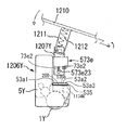
図2を参照して、イエローに対応した作像部6Yは、感光体ドラム1Yと、感光体ドラム1Yの周囲に配設された帯電部4Y、現像装置5Y(現像部)、クリーニング部2Y、不図示の除電部等で構成されている。作像部6Yでは、感光体ドラム1Y上で、作像プロセス(帯電工程、露光工程、現像工程、転写工程、クリーニング工程)がおこなわれて、感光体ドラム1Y上にイエロー画像が形成されることになる。
Referring to FIG. 2, an image forming unit 6Y corresponding to yellow includes a photosensitive drum 1Y, a charging unit 4Y disposed around the photosensitive drum 1Y, a developing device 5Y (developing unit), a cleaning unit 2Y, It consists of a static elimination unit (not shown). In the image forming unit 6Y, an image forming process (charging process, exposure process, developing process, transfer process, cleaning process) is performed on the photosensitive drum 1Y, and a yellow image is formed on the photosensitive drum 1Y. become.
なお、他の3つの作像部6M、6C、6Kも、使用されるトナーの色が異なる以外は、イエローに対応した作像部6Yとほぼ同様の構成となっていて、それぞれのトナー色に対応した画像が形成される。以下、他の3つの作像部6M、6C、6Kの説明を適宜に省略して、イエローに対応した作像部6Yのみの説明を行なうことにする。
The other three image forming units 6M, 6C, and 6K have substantially the same configuration as that of the image forming unit 6Y corresponding to yellow except that the color of the toner used is different. A corresponding image is formed. Hereinafter, description of the other three image forming units 6M, 6C, and 6K will be omitted as appropriate, and only the image forming unit 6Y corresponding to yellow will be described.
図2を参照して、感光体ドラム1Yは、不図示の駆動モータによって図2中の時計方向に回転駆動される。そして、帯電部4Yの位置で、感光体ドラム1Yの表面が一様に帯電される(帯電工程である)。感光体ドラム1Yの表面は、露光装置7(図1を参照できる)から発せられたレーザ光Lの照射位置に達して、この位置での露光走査によってイエローに対応した静電潜像が形成される(露光工程である)。
Referring to FIG. 2, the photosensitive drum 1Y is driven to rotate clockwise in FIG. 2 by a drive motor (not shown). Then, the surface of the photosensitive drum 1Y is uniformly charged at the position of the charging unit 4Y (charging process). The surface of the photosensitive drum 1Y reaches the irradiation position of the laser beam L emitted from the exposure device 7 (see FIG. 1), and an electrostatic latent image corresponding to yellow is formed by exposure scanning at this position. (It is an exposure process).
感光体ドラム1Yの表面は、現像装置5Yとの対向位置に達して、この位置で静電潜像が現像されて、イエローのトナー像が形成される(現像工程である)。感光体ドラム1Yの表面は、中間転写ベルト8及び第1転写バイアスローラ9Yとの対向位置に達して、この位置で感光体ドラム1Y上のトナー像が中間転写ベルト8上に転写される(1次転写工程である)。このとき、感光体ドラム1Y上には、僅かながら未転写トナーが残存する。
The surface of the photosensitive drum 1Y reaches a position facing the developing device 5Y, and the electrostatic latent image is developed at this position to form a yellow toner image (this is a developing process). The surface of the photosensitive drum 1Y reaches a position facing the intermediate transfer belt 8 and the first transfer bias roller 9Y, and the toner image on the photosensitive drum 1Y is transferred onto the intermediate transfer belt 8 at this position (1). Next transfer step). At this time, a small amount of untransferred toner remains on the photosensitive drum 1Y.
その後、感光体ドラム1Yの表面は、クリーニング部2Yとの対向位置に達して、この位置で感光体ドラム1Y上に残存した未転写トナーがクリーニングブレード2aによって機械的に回収される(クリーニング工程である)。最後に、感光体ドラム1Yの表面は、不図示の除電部との対向位置に達して、この位置で感光体ドラム1Y上の残留電位が除去される。こうして、感光体ドラム1Y上で行われる、一連の作像プロセスが終了する。
Thereafter, the surface of the photosensitive drum 1Y reaches a position facing the cleaning unit 2Y, and untransferred toner remaining on the photosensitive drum 1Y at this position is mechanically collected by the cleaning blade 2a (in the cleaning process). is there). Finally, the surface of the photosensitive drum 1Y reaches a position facing a neutralization unit (not shown), and the residual potential on the photosensitive drum 1Y is removed at this position. Thus, a series of image forming processes performed on the photosensitive drum 1Y is completed.
なお、上述した作像プロセスは、他の作像部6M、6C、6Kでも、イエローの作像部6Yと同様に行われる。すなわち、作像部の下方に配設された露光部7から、画像情報に基いたレーザ光Lが、各作像部6M、6C、6Kの感光体ドラム上に向けて照射される。詳しくは、露光部7は、光源からレーザ光Lを発して、そのレーザ光Lを回転駆動されたポリゴンミラーで走査しながら、複数の光学素子を介して感光体ドラム上に照射する。その後、現像工程を経て各感光体ドラム上に形成した各色のトナー像を、中間転写ベルト8上に重ねて転写する。こうして、中間転写ベルト8上にカラー画像が形成される。
The image forming process described above is performed in the other image forming units 6M, 6C, and 6K in the same manner as the yellow image forming unit 6Y. That is, the laser beam L based on the image information is emitted from the exposure unit 7 disposed below the image forming unit onto the photosensitive drums of the image forming units 6M, 6C, and 6K. Specifically, the exposure unit 7 emits laser light L from a light source, and irradiates the photosensitive drum through a plurality of optical elements while scanning the laser light L with a polygon mirror that is rotationally driven. Thereafter, the toner images of the respective colors formed on the respective photosensitive drums through the developing process are transferred onto the intermediate transfer belt 8 in an overlapping manner. In this way, a color image is formed on the intermediate transfer belt 8.
ここで、図1を参照して、中間転写ユニット15は、中間転写ベルト8、4つの1次転写バイアスローラ9Y、9M、9C、9K、2次転写バックアップローラ12、複数のテンションローラ、中間転写クリーニング部等で構成される。中間転写ベルト8は、複数のローラ部材によって張架・支持されると共に、2次転写バックアップローラ12の回転駆動によって図1中の矢印方向に無端移動される。
Here, referring to FIG. 1, the intermediate transfer unit 15 includes an intermediate transfer belt 8, four primary transfer bias rollers 9Y, 9M, 9C, 9K, a secondary transfer backup roller 12, a plurality of tension rollers, and an intermediate transfer. Consists of a cleaning unit and the like. The intermediate transfer belt 8 is stretched and supported by a plurality of roller members, and is endlessly moved in the direction of the arrow in FIG. 1 by the rotational drive of the secondary transfer backup roller 12.
4つの1次転写バイアスローラ9Y、9M、9C、9Kは、それぞれ、中間転写ベルト8を感光体ドラム1Y、1M、1C、1Kとの間に挟み込んで1次転写ニップを形成している。そして、1次転写バイアスローラ9Y、9M、9C、9Kに、トナーの極性とは逆の転写バイアスが印加される。中間転写ベルト8は、矢印方向に走行して、各1次転写バイアスローラ9Y、9M、9C、9Kの1次転写ニップを順次通過する。こうして、感光体ドラム1Y、1M、1C、1K上の各色のトナー像が、中間転写ベルト8上に重ねて1次転写される。
The four primary transfer bias rollers 9Y, 9M, 9C, and 9K respectively sandwich the intermediate transfer belt 8 with the photosensitive drums 1Y, 1M, 1C, and 1K to form a primary transfer nip. Then, a transfer bias reverse to the polarity of the toner is applied to the primary transfer bias rollers 9Y, 9M, 9C, and 9K. The intermediate transfer belt 8 travels in the direction of the arrow and sequentially passes through the primary transfer nips of the primary transfer bias rollers 9Y, 9M, 9C, and 9K. In this way, the toner images of the respective colors on the photosensitive drums 1Y, 1M, 1C, and 1K are primarily transferred while being superimposed on the intermediate transfer belt 8.
その後、各色のトナー像が重ねて転写された中間転写ベルト8は、2次転写ローラ19との対向位置に達する。この位置では、2次転写バックアップローラ12が、2次転写ローラ19との間に中間転写ベルト8を挟み込んで2次転写ニップを形成している。中間転写ベルト8上に形成された4色のトナー像は、この2次転写ニップの位置に搬送された転写紙等の記録媒体P上に転写される。このとき、中間転写ベルト8には、記録媒体Pに転写されなかった未転写トナーが残存する。
Thereafter, the intermediate transfer belt 8 on which the toner images of the respective colors are transferred in a superimposed manner reaches a position facing the secondary transfer roller 19. At this position, the secondary transfer backup roller 12 sandwiches the intermediate transfer belt 8 with the secondary transfer roller 19 to form a secondary transfer nip. The four-color toner images formed on the intermediate transfer belt 8 are transferred onto a recording medium P such as transfer paper conveyed to the position of the secondary transfer nip. At this time, untransferred toner that has not been transferred to the recording medium P remains on the intermediate transfer belt 8.
中間転写ベルト8は、不図示の中間転写クリーニング部の位置に達する。そして、この位置で、中間転写ベルト8上の未転写トナーが回収される。こうして、中間転写ベルト8上で行われる、一連の転写プロセスが終了する。
The intermediate transfer belt 8 reaches the position of an intermediate transfer cleaning unit (not shown). At this position, the untransferred toner on the intermediate transfer belt 8 is collected. Thus, a series of transfer processes performed on the intermediate transfer belt 8 is completed.
ここで、2次転写ニップの位置に搬送された記録媒体Pは、装置本体100の下方に配設された給紙部26から、給紙ローラ27やレジストローラ対28等を経由して搬送されたものである。詳しくは、給紙部26には、転写紙等の記録媒体Pが複数枚重ねて収納されている。そして、給紙ローラ27が図1中の反時計方向に回転駆動されると、一番上の記録媒体Pがレジストローラ対28のローラ間に向けて給送される。
Here, the recording medium P transported to the position of the secondary transfer nip is transported from a paper feeding unit 26 disposed below the apparatus main body 100 via a paper feeding roller 27, a registration roller pair 28, and the like. It is a thing. Specifically, a plurality of recording media P such as transfer paper are stored in the paper supply unit 26 in a stacked manner. When the paper feed roller 27 is driven to rotate counterclockwise in FIG. 1, the uppermost recording medium P is fed toward the rollers of the registration roller pair 28.
レジストローラ対28に搬送された記録媒体Pは、回転駆動を停止したレジストローラ対28のローラニップの位置で一旦停止する。そして、中間転写ベルト8上のカラー画像にタイミングを合わせて、レジストローラ対28が回転駆動されて、記録媒体Pが2次転写ニップに向けて搬送される。こうして、記録媒体P上に、所望のカラー画像が転写される。
The recording medium P transported to the registration roller pair 28 temporarily stops at the position of the roller nip of the registration roller pair 28 whose rotation drive has been stopped. Then, the registration roller pair 28 is rotationally driven in synchronization with the color image on the intermediate transfer belt 8, and the recording medium P is conveyed toward the secondary transfer nip. In this way, a desired color image is transferred onto the recording medium P.
その後、2次転写ニップの位置でカラー画像が転写された記録媒体Pは、定着装置20の位置に搬送される。そして、この位置で、定着ベルト及び加圧ローラによる熱と圧力とにより、表面に転写されたカラー画像が記録媒体P上に定着される。記録媒体Pは、排紙ローラ対29のローラ間を経て、装置外へと排出される。排紙ローラ対29によって装置外に排出された記録媒体Pは、出力画像として、スタック部30上に順次スタックされる。こうして、画像形成装置における、一連の画像形成プロセスが完了する。
Thereafter, the recording medium P on which the color image is transferred at the position of the secondary transfer nip is conveyed to the position of the fixing device 20. At this position, the color image transferred to the surface is fixed on the recording medium P by heat and pressure generated by the fixing belt and the pressure roller. The recording medium P is discharged out of the apparatus through a pair of paper discharge rollers 29. The recording media P discharged to the outside of the apparatus by the discharge roller pair 29 are sequentially stacked on the stack unit 30 as an output image. Thus, a series of image forming processes in the image forming apparatus is completed.
次に、図2にて、作像部における現像装置の構成・動作について、さらに詳しく説明する。
現像装置5Yは、感光体ドラム1Yに対向する現像ローラ51Y、現像ローラ51Yに対向するドクターブレード52Y、現像剤収容部53Y、54Y内に配設された2つの搬送スクリュ55Yを備えている。現像装置5Yは、現像剤中のトナー濃度を検知する濃度検知センサ56Y、を備えている。現像ローラ51Yは、内部に固設されたマグネットや、マグネットの周囲を回転するスリーブ等で構成される。現像剤収容部53Y、54Y内には、キャリアとトナーとからなる2成分現像剤Gが収容されている。現像剤収容部54Yは、その上方に形成された開口を介してトナー落下搬送経路64Yに連通している。
Next, the configuration and operation of the developing device in the image forming unit will be described in more detail with reference to FIG.
The developing device 5Y includes a developing roller 51Y that faces the photosensitive drum 1Y, a doctor blade 52Y that faces the developing roller 51Y, and two conveying screws 55Y that are disposed in the developer accommodating portions 53Y and 54Y. The developing device 5Y includes a density detection sensor 56Y that detects the toner density in the developer. The developing roller 51Y includes a magnet fixed inside, a sleeve rotating around the magnet, and the like. In the developer accommodating portions 53Y and 54Y, a two-component developer G composed of a carrier and a toner is accommodated. The developer accommodating portion 54Y communicates with the toner dropping conveyance path 64Y through an opening formed thereabove.
このように構成された現像装置5Yは、次のように動作する。現像ローラ51Yのスリーブは、図2の矢印方向に回転している。そして、マグネットにより形成された磁界によって現像ローラ51Y上に担持された現像剤Gは、スリーブの回転に伴い現像ローラ51Y上を移動する。
The developing device 5Y configured as described above operates as follows. The sleeve of the developing roller 51Y rotates in the direction of the arrow in FIG. The developer G carried on the developing roller 51Y by the magnetic field formed by the magnet moves on the developing roller 51Y as the sleeve rotates.
ここで、現像装置5Y内の現像剤Gは、現像剤中のトナーの割合(トナー濃度)が所定の範囲内になるように調整される。詳しくは、現像装置5Y内のトナー消費に応じて、トナー容器32Yに収容されているトナーが、トナー補給装置60Y(図3等を参照できる)を介して現像剤収容部54Y内に補給される。なお、トナー補給装置の構成・動作については、後で詳しく説明する。
Here, the developer G in the developing device 5Y is adjusted so that the ratio of toner in the developer (toner concentration) is within a predetermined range. Specifically, according to toner consumption in the developing device 5Y, the toner stored in the toner container 32Y is supplied into the developer storage portion 54Y via the toner supply device 60Y (see FIG. 3 and the like). . The configuration and operation of the toner supply device will be described in detail later.
その後、現像剤収容部54Y内に補給されたトナーは、2つの搬送スクリュ55Yによって、現像剤Gと共に混合・撹拌されながら、2つの現像剤収容部53Y、54Yを循環する(図2の紙面垂直方向の移動である)。そして、現像剤G中のトナーは、キャリアとの摩擦帯電によりキャリアに吸着して、現像ローラ51Y上に形成された磁力によりキャリアと共に現像ローラ51Y上に担持される。
Thereafter, the toner replenished in the developer accommodating portion 54Y is circulated through the two developer accommodating portions 53Y and 54Y while being mixed and stirred together with the developer G by the two conveying screws 55Y (perpendicular to the paper surface in FIG. 2). Direction movement). The toner in the developer G is attracted to the carrier by frictional charging with the carrier, and is carried on the developing roller 51Y together with the carrier by the magnetic force formed on the developing roller 51Y.
現像ローラ51Y上に担持された現像剤Gは、図2中の矢印方向に搬送されて、ドクターブレード52Yの位置に達する。そして、現像ローラ51Y上の現像剤Gは、この位置で現像剤量が適量化された後に、感光体ドラム1Yとの対向位置(現像領域である。)まで搬送される。そして、現像領域に形成された電界によって、感光体ドラム1Y上に形成された潜像にトナーが吸着される。その後、現像ローラ51Y上に残った現像剤Gはスリーブの回転に伴い現像剤収容部53Yの上方に達して、この位置で現像ローラ51Yから離脱される。
The developer G carried on the developing roller 51Y is conveyed in the direction of the arrow in FIG. 2 and reaches the position of the doctor blade 52Y. The developer G on the developing roller 51Y is conveyed to a position facing the photosensitive drum 1Y (development region) after the developer amount is made appropriate at this position. The toner is attracted to the latent image formed on the photosensitive drum 1Y by the electric field formed in the development area. Thereafter, the developer G remaining on the developing roller 51Y reaches above the developer containing portion 53Y as the sleeve rotates, and is detached from the developing roller 51Y at this position.
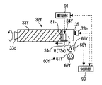
次に、図3〜図5にて、トナー補給装置60Y、60M、60C、60Kについて詳述する。図3を参照して、画像形成装置本体100のトナー容器収容部70に設置された各トナー容器32Y、32M、32C、32K内にはトナーが収納されている。これらトナーは、各色の現像装置内のトナー消費に応じて、トナー色ごとに設けられたトナー補給装置60Y、60M、60C、60Kによって適宜に各現像装置内に補給される。
なお、4つのトナー補給装置60Y、60M、60C、60Kやトナー容器32Y、32M、32C、32Kは、作像プロセスに用いられるトナーの色が異なる以外はほぼ同一構造である。このため、イエローに対応したトナー補給装置50Yやトナー容器32Yのみの説明をおこない、他の3つの色に対応したトナー補給装置60M、60C、60Kやトナー容器32M、32C、32Kの説明を適宜に省略する。
Next, the toner replenishing devices 60Y, 60M, 60C, and 60K will be described in detail with reference to FIGS. Referring to FIG. 3, toner is stored in toner containers 32Y, 32M, 32C, and 32K installed in toner container storage portion 70 of image forming apparatus main body 100. These toners are appropriately replenished into the developing devices by toner replenishing devices 60Y, 60M, 60C, and 60K provided for the respective toner colors in accordance with the consumption of toner in the developing devices of the respective colors.
The four toner replenishing devices 60Y, 60M, 60C, and 60K and the toner containers 32Y, 32M, 32C, and 32K have substantially the same structure except that the colors of toner used in the image forming process are different. Therefore, only the toner replenishing device 50Y and the toner container 32Y corresponding to yellow will be described, and the toner replenishing devices 60M, 60C and 60K and the toner containers 32M, 32C and 32K corresponding to the other three colors will be described as appropriate. Omitted.
ここで、図1を参照して、画像形成装置本体100の手前側(図1の紙面垂直方向手前側である)に設置された本体カバー(不図示である。)を開放すると、トナー容器収容部70(挿入口部71)が露呈される。そして、各トナー容器32Y、32M、32C、32Kの長手方向を水平方向とした状態で、画像形成装置本体100の手前側から各トナー容器32Y、32M、32C、32Kの着脱操作(トナー容器の長手方向を着脱方向とする着脱操作である。)が行われる。
Here, referring to FIG. 1, when a main body cover (not shown) installed on the front side of the image forming apparatus main body 100 (the front side in the direction perpendicular to the paper in FIG. 1) is opened, the toner container is accommodated. The part 70 (insertion port 71) is exposed. Then, with the longitudinal direction of the toner containers 32Y, 32M, 32C, and 32K set to the horizontal direction, the toner containers 32Y, 32M, 32C, and 32K can be attached and detached from the front side of the image forming apparatus main body 100 (the length of the toner containers). This is an attachment / detachment operation in which the direction is the attachment / detachment direction.
図4に示すように、トナー容器32Y、32M、32C、32Kが画像形成装置本体100のトナー容器収容部70に装着(矢印Q方向の移動である)されると、その装着動作に連動して、トナー容器32Y、32M、32C、32Kのシャッタ部材34dが移動する。するとトナー排出口W(排出口)が開放されると共に、トナー補給装置32Y、32M、32C、32Kのトナー補給口73w(図3を参照できる)とトナー排出口Wとが連通する。これにより、トナー容器32Y、32M、32C、32K内に収容されたトナーが、トナー排出口Wから排出されて、トナー補給装置60Y、60M、60C、60Kのトナー補給口73wからトナータンク部61Y内に貯溜されることになる。
As shown in FIG. 4, when the toner containers 32Y, 32M, 32C, and 32K are attached to the toner container accommodating portion 70 of the image forming apparatus main body 100 (moving in the direction of arrow Q), the toner containers 32Y, 32M, 32C, and 32K are interlocked with the attaching operation. The shutter members 34d of the toner containers 32Y, 32M, 32C, and 32K move. Then, the toner discharge port W (discharge port) is opened, and the toner supply port 73w (see FIG. 3) of the toner supply devices 32Y, 32M, 32C, and 32K and the toner discharge port W communicate with each other. As a result, the toner accommodated in the toner containers 32Y, 32M, 32C, and 32K is discharged from the toner discharge port W, and is transferred from the toner supply port 73w of the toner supply devices 60Y, 60M, 60C, and 60K into the toner tank portion 61Y. Will be stored.
ここで、図3の模式図を参照して、トナー容器32Yは、略円筒状のトナーボトルであって、主として、トナー容器収容部70に非回転で保持されるキャップ部34Yと、ギア33cが一体的に形成された容器本体33Y(ボトル本体)とで構成されている。容器本体33Yは、キャップ部34Yに対して相対的に回転可能に保持されていて、駆動部91(駆動モータ、駆動ギア81等で構成されている。)によって図3の矢印方向に回転駆動される。そして、容器本体33Y自体が回転すると、容器本体33Yの内周面に螺旋状に形成された突起33bによって、トナー容器32Y(容器本体33Y)の内部に収容されたトナーが長手方向に搬送される。ここでは図3の左方から右方へ搬送され、キャップ部34Yのトナー排出口Wからトナーが排出される。すなわち、駆動部91によってトナー容器32Yの容器本体33Yが適宜に回転駆動されることで、トナータンク部61Yにトナーが適宜に供給される。なお、トナー容器32Y、32M、32C、32Kは、それぞれ、寿命に達したとき(収容するトナーがほとんどすべて消費されて空になったとき)に新品のものに交換される。
Here, referring to the schematic diagram of FIG. 3, the toner container 32 </ b> Y is a substantially cylindrical toner bottle. The toner container 32 </ b> Y mainly includes a cap part 34 </ b> Y that is non-rotatably held in the toner container housing part 70 and a gear 33 c. It is comprised by the container main body 33Y (bottle main body) formed integrally. The container body 33Y is rotatably held relative to the cap portion 34Y, and is rotationally driven in the direction of the arrow in FIG. 3 by a drive unit 91 (comprising a drive motor, a drive gear 81, etc.). The Then, when the container main body 33Y itself rotates, the toner contained in the toner container 32Y (container main body 33Y) is conveyed in the longitudinal direction by the protrusions 33b formed in a spiral shape on the inner peripheral surface of the container main body 33Y. . Here, the toner is conveyed from the left to the right in FIG. 3 and discharged from the toner discharge port W of the cap portion 34Y. That is, when the container main body 33Y of the toner container 32Y is appropriately rotated by the drive unit 91, the toner is appropriately supplied to the toner tank unit 61Y. Each of the toner containers 32Y, 32M, 32C, and 32K is replaced with a new one when it reaches the end of its life (when almost all the toner to be stored is consumed and emptied).
図3を参照して、トナー補給装置60Y、60M、60C、60Kは、トナー容器収容部70、トナータンク部61Y、トナー搬送スクリュ62Y、撹拌部材65Y、トナーエンドセンサ66Y、駆動部91等で構成されている。トナータンク部61Yは、トナー容器32Yのトナー排出口Wの下方に配設されていて、トナー容器32Yのトナー排出口Wから排出されたトナーが貯留される。トナータンク部61Yの底部は、トナー搬送スクリュ62Yの上流部に接続されている。
また、トナータンク部61Yの壁面(底部から所定高さの位置である)には、トナータンク部61Yに貯留されたトナーが所定量以下になったことを検知するトナーエンドセンサ66Yが設置されている。トナーエンドセンサ66Yによってトナータンク部61Yに貯留されたトナーが所定量以下になったことが制御部90にて検知(トナーエンド検知)される。すると、制御部90の制御により駆動部91(駆動ギア81)によってトナー容器32Yの容器本体33Yを所定時間回転駆動してトナータンク部61Yへのトナー補給を行なう。さらに、このような制御を繰り返してもトナーエンドセンサ66Yによるトナーエンド検知が解除されない場合には、トナー容器32Y内にトナーがないものとして、画像形成装置本体100の不図示の表示部にトナー容器32Yの交換を促す旨の表示を行なう。
Referring to FIG. 3, toner replenishing devices 60Y, 60M, 60C, and 60K include a toner container housing portion 70, a toner tank portion 61Y, a toner conveying screw 62Y, a stirring member 65Y, a toner end sensor 66Y, a driving portion 91, and the like. Has been. The toner tank 61Y is disposed below the toner discharge port W of the toner container 32Y, and stores toner discharged from the toner discharge port W of the toner container 32Y. The bottom of the toner tank 61Y is connected to the upstream part of the toner conveying screw 62Y.
Further, a toner end sensor 66Y that detects that the amount of toner stored in the toner tank 61Y has become a predetermined amount or less is installed on the wall surface of the toner tank 61Y (at a predetermined height from the bottom). Yes. The control unit 90 detects (toner end detection) that the toner stored in the toner tank 61Y has become a predetermined amount or less by the toner end sensor 66Y. Then, under the control of the control unit 90, the drive unit 91 (drive gear 81) rotates the container body 33Y of the toner container 32Y for a predetermined time to supply toner to the toner tank unit 61Y. Further, if the toner end detection by the toner end sensor 66Y is not canceled even if such control is repeated, it is assumed that there is no toner in the toner container 32Y, and a toner container is displayed on a display unit (not shown) of the image forming apparatus main body 100. A display for prompting replacement of 32Y is performed.
トナータンク部61Yの中央(トナーエンドセンサ66Yの近傍である)には、トナータンク部61Yに貯留されたトナーの凝集を防ぐ撹拌部材65Yが設置されている。撹拌部材65Yは、軸部に可撓性部材が設置されたものであって、図3の時計方向に回転することによりトナータンク部61Y内のトナーを撹拌する。さらに、撹拌部材65Yの可撓性部材の先端が、回転周期でトナーエンドセンサ66Yの検知面に摺接することで、トナーエンドセンサ66Yの検知面にトナーが固着して検知精度が低下する不具合を抑止している。
In the center of the toner tank portion 61Y (in the vicinity of the toner end sensor 66Y), a stirring member 65Y that prevents aggregation of the toner stored in the toner tank portion 61Y is installed. The agitating member 65Y is provided with a flexible member at the shaft portion, and agitates the toner in the toner tank portion 61Y by rotating clockwise in FIG. Further, the tip of the flexible member of the stirring member 65Y is in sliding contact with the detection surface of the toner end sensor 66Y at a rotation cycle, so that the toner adheres to the detection surface of the toner end sensor 66Y and the detection accuracy decreases. Suppressed.
トナー搬送スクリュ62Yは、トナータンク部61Yの底部(最下点)から現像装置5Yの上方に向けてトナーを直線的に搬送する。そして、トナー搬送スクリュ62Yによって搬送されたトナーは、トナー落下搬送経路64Y(図2を参照できる。)を自重落下して現像装置5Y(現像剤収容部54Y)内に補給される。
The toner conveying screw 62Y linearly conveys the toner from the bottom (lowermost point) of the toner tank 61Y toward the upper side of the developing device 5Y. Then, the toner transported by the toner transport screw 62Y falls in its own weight on the toner drop transport path 64Y (see FIG. 2) and is replenished into the developing device 5Y (developer container 54Y).
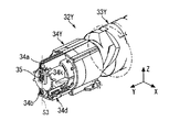
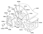
図4を参照して、トナー容器収容部70は、主として、トナー容器32Yのキャップ部34Yを保持するための装着部となるキャップ受部73を備えている。トナー容器収容部70は、トナー容器32Yの容器本体33Yを保持するためのボトル受部72(容器本体受部)と、トナー容器32Yの装着動作時における挿入口となる挿入口部71とを備えている。
Referring to FIG. 4, the toner container housing portion 70 mainly includes a cap receiving portion 73 serving as a mounting portion for holding the cap portion 34Y of the toner container 32Y. The toner container housing part 70 includes a bottle receiving part 72 (container main body receiving part) for holding the container main body 33Y of the toner container 32Y, and an insertion opening 71 serving as an insertion opening during the mounting operation of the toner container 32Y. ing.
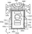
次に、図6〜図12等にて、トナー容器収容部70(ボトル受部72、キャップ受部73)について詳述する。
先に図4、図5にて説明したように、トナー容器収容部70には、ボトル受部72やキャップ受部73や挿入口部71(図5では図示が省略されている)が設けられている。そして、トナー容器32Yは、把持部33dを把持するユーザーによって、長手方向を水平方向とした状態で、容器本体33Yに対してキャップ部34Yを先頭にして長手方向を装着方向として、挿入口部71からトナー容器収容部70に装着される。挿入口部71から挿入されたトナー容器32Yは、ボトル受部72のボトル受面72a(図5、図6をも参照できる)を滑動しながら、キャップ受部73に向けてユーザーによって押し込まれる。ここで、図6等を参照して、ボトル受部72には、色毎にボトル受面72aが形成されていて、それぞれに対応するトナー容器32Y、32M、32C、32Kが挿入される(白矢印方向の挿入である)。さらに、図8を参照して、キャップ受部73にも、色毎にボトル受部73Y、73M、73C、73Kが形成されている。ボトル受部73Y、73M、73C、73Kは、それぞれに対応するトナー容器32Y、32M、32C、32Kが挿入(白矢印方向の挿入である)される。キャップ部は、トナー容器32Y、32M、32C、32Kが挿入された位置において非回転で保持される。
Next, the toner container housing portion 70 (bottle receiving portion 72, cap receiving portion 73) will be described in detail with reference to FIGS.
As described above with reference to FIGS. 4 and 5, the toner container housing portion 70 is provided with the bottle receiving portion 72, the cap receiving portion 73, and the insertion port portion 71 (not shown in FIG. 5). ing. The toner container 32Y is inserted into the insertion port 71 by the user holding the holding portion 33d, with the longitudinal direction set as the mounting direction with the cap portion 34Y leading to the container main body 33Y in the horizontal direction. To the toner container housing 70. The toner container 32Y inserted from the insertion opening 71 is pushed by the user toward the cap receiving portion 73 while sliding on the bottle receiving surface 72a of the bottle receiving portion 72 (see FIGS. 5 and 6). Here, referring to FIG. 6 and the like, a bottle receiving surface 72a is formed for each color in the bottle receiving portion 72, and corresponding toner containers 32Y, 32M, 32C, 32K are inserted (white). Insertion in the direction of the arrow). Further, referring to FIG. 8, the bottle receivers 73 </ b> Y, 73 </ b> M, 73 </ b> C, and 73 </ b> K are also formed in the cap receiver 73 for each color. In the bottle receiving portions 73Y, 73M, 73C, and 73K, corresponding toner containers 32Y, 32M, 32C, and 32K are inserted (in the direction of white arrows). The cap part is held non-rotatably at the position where the toner containers 32Y, 32M, 32C, 32K are inserted.
図5を参照して、トナー容器収容部70のボトル受部72には、ボトル受面72a、ストッパ解除付勢部72b等が設けられている。ボトル受面72aは、図6に示すように、トナー容器32Yの着脱動作時にはトナー容器32Yの滑動面として機能し、トナー容器32Yのセットが完了した後には回転駆動する容器本体33Yの保持部として機能する。図5を参照して、ストッパ解除付勢部72bは、ボトル受面72aの上方(トナー容器32Yの装着方向下流側である)に形成された台形状のリブである。ストッパ解除付勢部72bは、トナー容器32Yの装着動作に連動して、シャッタ部材34Yの図示しないストッパ解除部1を押し上げてストッパ部と当接部との当接状態を解除するためのものである。
Referring to FIG. 5, the bottle receiving portion 72 of the toner container housing portion 70 is provided with a bottle receiving surface 72a, a stopper release urging portion 72b, and the like. As shown in FIG. 6, the bottle receiving surface 72a functions as a sliding surface of the toner container 32Y when the toner container 32Y is attached and detached, and as a holding portion of the container body 33Y that is rotationally driven after the setting of the toner container 32Y is completed. Function. Referring to FIG. 5, stopper release urging portion 72b is a trapezoidal rib formed above bottle receiving surface 72a (on the downstream side in the mounting direction of toner container 32Y). The stopper release urging portion 72b is for releasing the contact state between the stopper portion and the contact portion by pushing up the stopper release portion 1 (not shown) of the shutter member 34Y in conjunction with the mounting operation of the toner container 32Y. is there.
図9、図10を参照して、トナー容器収容部70のキャップ受部73には、主基準ピン73a、従基準ピン73b、被当接溝73m、壁部73g、貫通穴73f等が設けられている。位置決めピンとしての主基準ピン73a及び従基準ピン73bは、それぞれ、図12に示すトナー容器32Yにおけるキャップ部34Yの第1の位置決め穴部34aと第2の位置決め穴部34bとに嵌合する。そして、キャップ受部73におけるキャップ部34Yの位置決めが行われる。
ここで、図7等を参照して、主基準ピン73aは、従基準ピン73bよりも長手方向に長く形成されている(根元部となる基準面の位置は同一平面上に形成されている)。また、主基準ピン73aは、その先端部が先細り形状となっている。これらにより、キャップ受部73へのトナー容器32Yの長手方向の装着動作において、キャップ受部73へのトナー容器32Yのスムーズな装着が可能になる。
Referring to FIGS. 9 and 10, the cap receiving portion 73 of the toner container housing portion 70 is provided with a main reference pin 73a, a sub reference pin 73b, a contact groove 73m, a wall portion 73g, a through hole 73f, and the like. ing. The main reference pin 73a and the secondary reference pin 73b as positioning pins are fitted into the first positioning hole 34a and the second positioning hole 34b of the cap 34Y in the toner container 32Y shown in FIG. Then, positioning of the cap portion 34Y in the cap receiving portion 73 is performed.
Here, referring to FIG. 7 and the like, the main reference pin 73a is formed longer in the longitudinal direction than the sub-reference pin 73b (the position of the reference surface serving as the root portion is formed on the same plane). . The main reference pin 73a has a tapered tip. Accordingly, the toner container 32Y can be smoothly attached to the cap receiving part 73 in the operation of attaching the toner container 32Y to the cap receiving part 73 in the longitudinal direction.
図9、図10を参照して、被当接溝73mはキャップ受部73の内壁であって主基準ピン73aの上方に主基準ピン73aの先端部よりも装着方向上流側から溝状に形成された凹部である。被当接溝73mは、後述するトナー容器32Yのキャップ部34Yの外周上方に長手方向に延在するように形成された図示しないガイドレール部34eが、主基準ピン73aの位置決め穴34aへの挿入に先立って嵌りこむようになっている。
Referring to FIGS. 9 and 10, the contact groove 73m is an inner wall of the cap receiving portion 73 and is formed in a groove shape above the main reference pin 73a from the upstream side in the mounting direction with respect to the front end portion of the main reference pin 73a. Recessed portion. In the contact groove 73m, a guide rail portion 34e (not shown) formed so as to extend in the longitudinal direction above the outer periphery of a cap portion 34Y of the toner container 32Y described later is inserted into the positioning hole 34a of the main reference pin 73a. It is designed to be inserted in advance.
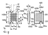
また、図9、図10等を参照して、キャップ受部73の奥側壁面(装着方向奥側において鉛直方向に起立する壁面である)には、鉛直方向に延在する長円穴と方形穴とが互いの縁線を一致させて重なった状態の形状からなる貫通穴73fが形成されている。そして、この貫通穴73fを介して、後述するコネクタ73e(図11を参照できる)が、キャップ受け部73の内壁側に露呈するように設置される(図12)等を参照できる)。キャップ受部73(画像形成装置本体100)にトナー容器32Yが装着されると、そのキャップ部34Yの先端に配された情報記憶装置としてのIDチップ35に対してコネクタ73eが対向接触する。そして、IDチップ35と装置本体100(制御部90)との間での情報通信が可能になる。
In addition, referring to FIGS. 9 and 10, an oblong hole and a square extending in the vertical direction are formed on the back side wall surface of the cap receiving portion 73 (a wall surface standing in the vertical direction on the back side in the mounting direction). A through hole 73f having a shape in which the hole overlaps with the edge line of each other is formed. A connector 73e (see FIG. 11), which will be described later, is installed through the through hole 73f so as to be exposed on the inner wall side of the cap receiving portion 73 (see FIG. 12). When the toner container 32Y is attached to the cap receiving portion 73 (image forming apparatus main body 100), the connector 73e comes into contact with the ID chip 35 serving as an information storage device disposed at the tip of the cap portion 34Y. Then, information communication between the ID chip 35 and the apparatus main body 100 (control unit 90) becomes possible.
次に、トナー容器収容部70のキャップ受部73へのコネクタ73eの設置形態について述べる。
図8を参照して、イエロー、マゼンタ、シアン、ブラックの各色トナー容器32Y、32M、32C、32Kに対応して4つのコネクタ73eが、各キャップ受部73に配置されている。4つのコネクタ73eは、1つの長方形の共通電子基板95上に並設されている。詳しくは、図11に示すコネクタ73eの底部に形成されたスナップフィット73e4を、共通電子基板95に形成された不図示の穴部に嵌め込むことで、共通電子基板95上にコネクタ73eを固定している。
図8、図12を参照して、4つのコネクタ73eが固定された共通電子基板95は、4つのコネクタ73eがそれぞれ貫通孔73fを介してキャップ受部73の内部に入り込んだ状態で架設・固定される。4つのコネクタ73eは4つのキャップ受部73K、73C、73M、73Yの配列方向に沿うように共通電子基板95は固定されている。詳しくは、4つのネジ99が、共通電子基板95に形成された穴部を介して、4つのキャップ受部73K、73C、73M、73Yの外壁部の下方に形成された雌ネジ部73xにそれぞれ螺合される。これにより、キャップ受部73に対して共通電子基板95が外側からネジ締結されている。
Next, an installation mode of the connector 73e to the cap receiving portion 73 of the toner container housing portion 70 will be described.
Referring to FIG. 8, four connectors 73e are arranged in each cap receiving portion 73 corresponding to the yellow, magenta, cyan, and black color toner containers 32Y, 32M, 32C, and 32K. The four connectors 73e are arranged side by side on one rectangular common electronic board 95. Specifically, the connector 73e is fixed on the common electronic board 95 by fitting a snap fit 73e4 formed on the bottom of the connector 73e shown in FIG. 11 into a hole (not shown) formed in the common electronic board 95. ing.
8 and 12, the common electronic board 95 to which the four connectors 73e are fixed is installed and fixed in a state where the four connectors 73e enter the inside of the cap receiving portion 73 through the through holes 73f, respectively. Is done. The common electronic substrate 95 is fixed so that the four connectors 73e are along the arrangement direction of the four cap receiving portions 73K, 73C, 73M, and 73Y. Specifically, the four screws 99 are respectively connected to the female screw portions 73x formed below the outer wall portions of the four cap receiving portions 73K, 73C, 73M, and 73Y through the holes formed in the common electronic substrate 95. Screwed together. Thereby, the common electronic substrate 95 is screwed to the cap receiving portion 73 from the outside.
以下、コネクタ73eの構成・動作について述べる。
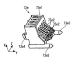
図11を参照して、コネクタ73eは、コネクタ本体73e1、4つの本体側端子73e2、2つの位置決めピン73e3(位置決め用の突起部)等で構成されている。コネクタ73eにおける4つの本体側端子73e2は、それぞれ、板状(又は線状)の金属部材であって、その一端側を固定端として他端側を自由端としてコネクタ本体73e1に固定支持されている。また、4つの本体側端子73e2は、それぞれ、その他端側にIDチップ35の側に向けて湾曲した湾曲部(金属板としての金属パット35aとの接点となる部分である)が形成されている。そして、キャップ受部73へのキャップ部34Yの装着動作に伴い、本体側端子73e2の湾曲部は、図11のX方向に変位する。そして、キャップ部34Yに設置されたIDチップ35の金属パット35a(金属板)に対する接触圧を徐々に強めながら、長手方向中央部から図18の左方(第1の仮想直線S1近傍である)に向けてスライドすることになる。なお、図11に示すように、位置決めピン73e3の先端部は、IDチップ35の切欠部35b1との係合がスムーズに行われるように、テーパ状に形成されている。
Hereinafter, the configuration and operation of the connector 73e will be described.
Referring to FIG. 11, the connector 73e includes a connector main body 73e1, four main body side terminals 73e2, two positioning pins 73e3 (positioning protrusions), and the like. Each of the four main body side terminals 73e2 in the connector 73e is a plate-shaped (or linear) metal member, and is fixedly supported on the connector main body 73e1 with one end side as a fixed end and the other end side as a free end. . Each of the four main body side terminals 73e2 has a curved portion (a portion serving as a contact point with the metal pad 35a as a metal plate) that is curved toward the ID chip 35 side on the other end side. . As the cap portion 34Y is attached to the cap receiving portion 73, the bending portion of the main body side terminal 73e2 is displaced in the X direction in FIG. Then, while gradually increasing the contact pressure with respect to the metal pad 35a (metal plate) of the ID chip 35 installed in the cap portion 34Y, from the center in the longitudinal direction to the left in FIG. 18 (near the first virtual straight line S1). Will slide towards. As shown in FIG. 11, the tip of the positioning pin 73e3 is formed in a tapered shape so that the engagement with the notch 35b1 of the ID chip 35 is smoothly performed.
図9、図10、図12を参照して、壁部73gは、コネクタ73eが設置される貫通穴73fの下方及び側方を囲むように設置されている。壁部73gを設けることで、トナー容器32Yのトナー排出口Wの近傍から外部にトナーが飛散した場合でも、壁部73gによって飛散トナーが遮られるため、コネクタ73eやIDチップ35に飛散トナーが直接的に付着し難くなる。したがって、飛散トナーによるコネクタ73e(本体側端子73e2)とIDチップ35(金属パット35a)との接触不良(通信不良)を抑止することができる。
Referring to FIGS. 9, 10, and 12, wall portion 73 g is installed so as to surround the lower side and the side of through hole 73 f in which connector 73 e is installed. By providing the wall portion 73g, even when the toner scatters from the vicinity of the toner outlet W of the toner container 32Y to the outside, the scattered toner is blocked by the wall portion 73g, so that the scattered toner is directly applied to the connector 73e and the ID chip 35. It becomes difficult to adhere. Therefore, contact failure (communication failure) between the connector 73e (main body side terminal 73e2) and the ID chip 35 (metal pad 35a) due to scattered toner can be suppressed.
トナー容器32Y、32M、32C、32Kにそれぞれ設けられるIDチップ35と、画像形成装置本体100のコネクタ73eとが接触すると、両者の間で必要な情報の授受が行われる。双方の間で通信される情報としては、トナー容器やIDチップそのものの製造番号、製造日、リサイクル回数等の情報や、トナーの容量、ロット番号、色等の情報や、画像形成装置本体100の使用履歴等の情報がある。IDチップ35には、これらの電子情報が画像形成装置本体100に設置される前に予め記憶されている(又は、設置された後に画像形成装置本体100から受け取った情報が記憶される)。なお、IDチップ35については、後でさらに詳しく説明する。
When the ID chip 35 provided in each of the toner containers 32Y, 32M, 32C, and 32K contacts the connector 73e of the image forming apparatus main body 100, necessary information is exchanged between them. Information communicated between the two includes information such as the production number, production date, and number of recyclings of the toner container and the ID chip itself, information such as toner capacity, lot number, and color, and information on the image forming apparatus main body 100. There is information such as usage history. The electronic information is stored in the ID chip 35 before being installed in the image forming apparatus main body 100 (or information received from the image forming apparatus main body 100 after being installed). The ID chip 35 will be described in more detail later.
次に、図13〜図15を参照して、トナー容器32Y、32M、32C、32Kについて詳述する。トナー容器32Yは、主として、容器本体33Y(ボトル本体)と、その頭部に設けられたキャップ部34Y(ボトルキャップ)とで構成されている。キャップ部34Yには、シャッタ部材34d、IDチップ35等が分解可能に設置されている。
Next, the toner containers 32Y, 32M, 32C, and 32K will be described in detail with reference to FIGS. The toner container 32Y mainly includes a container main body 33Y (bottle main body) and a cap portion 34Y (bottle cap) provided on the head. The cap member 34Y is provided with a shutter member 34d, an ID chip 35, and the like that can be disassembled.
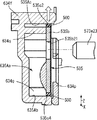
容器本体33Yの頭部には、図14に示すように、容器本体33Yと共に一体的に回転するギア33cと、開口部Aとが長手方向の一端側に設けられている。開口部Aは、容器本体33Yの頭部(装着動作において先方となる位置である)に設けられていて、容器本体33Y内に収容されたトナーをキャップ部34Y内の空洞に向けて排出するためのものである。なお、容器本体33Y内からキャップ部34Y内の空洞へのトナー搬送(容器本体33Yの回転駆動)は、画像形成装置本体側のトナー消費に応じて適宜に行われる。
As shown in FIG. 14, a gear 33c that rotates integrally with the container main body 33Y and an opening A are provided on one end side in the longitudinal direction at the head of the container main body 33Y. The opening A is provided at the head of the container main body 33Y (which is the front position in the mounting operation), and discharges the toner stored in the container main body 33Y toward the cavity in the cap 34Y. belongs to. The toner conveyance from the container main body 33Y to the cavity in the cap portion 34Y (the rotation driving of the container main body 33Y) is appropriately performed according to the toner consumption on the image forming apparatus main body side.
ギア33cは、画像形成装置本体100のトナー容器収容部70に設けられた駆動ギア81と噛合して、容器本体33Yを、回転軸を中心に回転駆動させるためのものである。詳しくは、ギア33cは、後述するキャップ部34Yの外周面に形成された切欠穴部34x(図13等を参照できる)から露呈して、画像形成装置本体100の駆動ギア81と噛合する。そして、駆動ギア81からギア33cに駆動力が伝達されて、容器本体33Yが時計方向に回転することになる。
The gear 33c is for meshing with a driving gear 81 provided in the toner container housing portion 70 of the image forming apparatus main body 100 to drive the container main body 33Y about the rotation axis. Specifically, the gear 33c is exposed from a notch hole portion 34x (see FIG. 13 and the like) formed on the outer peripheral surface of the cap portion 34Y, which will be described later, and meshes with the drive gear 81 of the image forming apparatus main body 100. Then, the driving force is transmitted from the driving gear 81 to the gear 33c, and the container body 33Y rotates in the clockwise direction.
図13を参照して、容器本体33Yの長手方向他端側(装着方向の後方の端部である)には、トナー容器32Yの着脱作業を行なう際にユーザーが把持するための把持部33dが設けられている。ユーザーは把持部33dを把持しながら、画像形成装置本体100に対してトナー容器32Yの装着を行なうことになる(図13の矢印方向へのトナー容器32Yの移動である)。
Referring to FIG. 13, on the other end side in the longitudinal direction of container main body 33Y (the rear end in the mounting direction), there is a gripping portion 33d for the user to grip when attaching / detaching toner container 32Y. Is provided. The user attaches the toner container 32Y to the image forming apparatus main body 100 while holding the holding part 33d (the movement of the toner container 32Y in the direction of the arrow in FIG. 13).
容器本体33Yの内周面には、螺旋状の突起33bが設けられている(外周面側から見ると螺旋状の溝となっている)。この螺旋状の突起33bは、容器本体33Yを所定方向に回転駆動して開口部Aからトナーを排出するためのものである。このように構成された容器本体33Yは、その周面上に配設されるギア33cや把持部33dと共にブロー成形にて製造することができる。
A spiral protrusion 33b is provided on the inner peripheral surface of the container main body 33Y (when viewed from the outer peripheral surface side, it is a spiral groove). The spiral projection 33b is for rotating and driving the container body 33Y in a predetermined direction to discharge the toner from the opening A. The container main body 33Y configured in this way can be manufactured by blow molding together with the gear 33c and the gripping portion 33d disposed on the peripheral surface thereof.
図14を参照して、容器本体33Yの頭部33Yc(ギア33cが形成された位置近傍である)の内径は、トナーが収容された収容部33Ya(螺旋状の突起33bが形成された位置である)の内径よりも小さくなるように形成されている。容器本体33Yにおいて、頭部33Ycと収容部33Yaとの間には、その内周面が内部に向かってせり出すように形成された汲み上げ部33Yb(図15の一点鎖線で囲んだ部分である)が設けられている。そして、容器本体33Yの回転に伴い螺旋状の突起33bによって開口部Aに向けて搬送されたトナーは、汲み上げ部33Ybによって頭部33Ycの小径部に汲み上げられる。その後、頭部33Ycの小径部に汲み上げられたトナーは、図示しない撹拌部材に撹拌されながら、開口部Aからキャップ部34Yの空洞に向けて排出される。
Referring to FIG. 14, the inner diameter of the head 33Yc (near the position where the gear 33c is formed) of the container body 33Y is the position where the toner is accommodated in the accommodating portion 33Ya (where the spiral protrusion 33b is formed). It is formed so as to be smaller than the inner diameter. In the container body 33Y, a pumping portion 33Yb (a portion surrounded by a one-dot chain line in FIG. 15) is formed between the head portion 33Yc and the accommodating portion 33Ya so that the inner peripheral surface protrudes toward the inside. Is provided. Then, the toner conveyed toward the opening A by the spiral protrusion 33b with the rotation of the container body 33Y is pumped to the small diameter portion of the head 33Yc by the pumping portion 33Yb. Thereafter, the toner pumped to the small diameter portion of the head portion 33Yc is discharged from the opening A toward the cavity of the cap portion 34Y while being stirred by a stirring member (not shown).
図15を参照して、キャップ部34Yの上部(天井部)には、長手方向に直交するキャップ部34Yの端面から長手方向に延設された第1の位置決め穴部34aが形成されている。この第1の位置決め穴部34aは、画像形成装置本体100におけるキャップ部34Yの位置決め主基準となる。詳しくは、トナー容器収容部70へのトナー容器32Yの長手方向の装着動作に連動して、キャップ部34Yの第1の位置決め穴部34aにキャップ受部73の位置決めピンとしての主基準ピン73a(図9、図12等を参照できる)が嵌合する。
また、キャップ部34Yの下部(底部)には、長手方向に直交するキャップ部34Yの端面から長手方向に延設された第2の位置決め穴部34bが、トナー排出口Wの位置に達しないように形成されている。この第2の位置決め穴部34bは、画像形成装置本体100におけるキャップ部34Yの位置決め従基準となる。詳しくは、トナー容器収容部70へのトナー容器32Yの長手方向の装着動作に連動して、キャップ部34Yの第2の位置決め穴部34bにキャップ受部73の位置決めピンとしての従基準ピン73b(図9、図12等を参照できる)が嵌合する。このように構成された2つの位置決め穴部34a、34bによって、トナー容器収容部70におけるキャップ部34Yの位置決めが行われる。
Referring to FIG. 15, a first positioning hole 34a extending in the longitudinal direction from the end surface of cap part 34Y orthogonal to the longitudinal direction is formed in the upper part (ceiling part) of cap part 34Y. The first positioning hole 34 a serves as a main positioning reference for the cap 34 </ b> Y in the image forming apparatus main body 100. Specifically, in conjunction with the operation of attaching the toner container 32Y in the longitudinal direction to the toner container housing portion 70, the main reference pin 73a (as a positioning pin of the cap receiving portion 73 is inserted into the first positioning hole portion 34a of the cap portion 34Y. 9 and 12 can be referred to).
Further, the second positioning hole 34b extending in the longitudinal direction from the end surface of the cap 34Y orthogonal to the longitudinal direction does not reach the position of the toner discharge port W at the lower portion (bottom) of the cap portion 34Y. Is formed. The second positioning hole 34b serves as a positioning reference for the cap 34Y in the image forming apparatus main body 100. Specifically, in accordance with the operation of mounting the toner container 32Y in the toner container housing portion 70 in the longitudinal direction, the secondary reference pin 73b (as a positioning pin of the cap receiving portion 73) is inserted into the second positioning hole 34b of the cap portion 34Y. 9 and 12 can be referred to). The positioning of the cap portion 34Y in the toner container housing portion 70 is performed by the two positioning holes 34a and 34b configured as described above.
以下、本実施の形態における着脱可能装置としてのトナー容器32Yの特徴的な、IDチップ35について詳述する。
図15、図16等を参照して、キャップ部34Yの端面上には、第1の位置決め穴部34aと第2の位置決め穴部34bとの間に設置された保持部を構成する保持部材34kの位置に、種々の電子情報が記憶されたIDチップ35が設置されている。IDチップ35は、トナー容器収容部70(キャップ受部73)にキャップ部34Yが装着された状態で、キャップ受部73のコネクタ73eに接続されるように構成されている(図3、図12等を参照できる)。具体的には、トナー容器収容部70(キャップ受部73)にキャップ部34Yが装着された状態で、IDチップ35の複数の金属パット35a(金属板)と、コネクタ73eの複数の本体側端子73e2とが接触する。そして、IDチップ35は、キャップ部34Yがキャップ受部73に保持された状態で、図3で示すようにコネクタ73eを介して制御部90との間で通信(有線通信)を行なう。
Hereinafter, the characteristic ID chip 35 of the toner container 32Y as the detachable device in the present embodiment will be described in detail.
Referring to FIGS. 15 and 16, etc., on the end surface of the cap portion 34Y, a holding member 34k constituting a holding portion installed between the first positioning hole portion 34a and the second positioning hole portion 34b. The ID chip 35 in which various electronic information is stored is installed at the position. The ID chip 35 is configured to be connected to the connector 73e of the cap receiving portion 73 in a state where the cap portion 34Y is attached to the toner container housing portion 70 (cap receiving portion 73) (FIGS. 3 and 12). Etc.). Specifically, the plurality of metal pads 35a (metal plate) of the ID chip 35 and the plurality of main body side terminals of the connector 73e in a state where the cap portion 34Y is attached to the toner container housing portion 70 (cap receiving portion 73). 73e2 contacts. The ID chip 35 performs communication (wired communication) with the control unit 90 via the connector 73e as shown in FIG. 3 in a state where the cap unit 34Y is held by the cap receiving unit 73.
図16〜図18を参照して、本実施の形態1において、画像形成装置本体100に対して着脱可能に設置されるトナー容器32Yに設置される保持機構は、IDチップ35、保持部材34k等で構成されている。また、保持機構に保持されるIDチップ35は、基板35b、情報記憶部35c、複数の端子としての金属パット35a(金属板)等で構成されている。
図18を参照して、情報記憶部35cは、画像形成装置本体100の制御部90とトナー容器32Yとの間でやり取りされる種々の情報が記憶されている電子回路である。図18では簡略のため斜線にて箱状のものとして表しているが、メモリーICやノイズ低減のためのコンデンサ、抵抗等の集合体が該当する。この情報記憶部35cは、基板35bの裏面35ba(本体側端子73e2と接触する面と反対の面)に配置されていて、複数の金属板としての金属パット35aの全部又は一部に電気的に接続されている。
Referring to FIGS. 16 to 18, in the first embodiment, the holding mechanism installed in toner container 32 </ b> Y that is detachably installed on image forming apparatus main body 100 includes an ID chip 35, a holding member 34 k, and the like. It consists of The ID chip 35 held by the holding mechanism includes a substrate 35b, an information storage unit 35c, a metal pad 35a (metal plate) as a plurality of terminals, and the like.
Referring to FIG. 18, the information storage unit 35 c is an electronic circuit that stores various types of information exchanged between the control unit 90 of the image forming apparatus main body 100 and the toner container 32 </ b> Y. In FIG. 18, for the sake of simplicity, it is represented as a box shape with diagonal lines, but it corresponds to an aggregate of memory ICs, capacitors for reducing noise, resistors, and the like. The information storage unit 35c is disposed on the back surface 35ba (the surface opposite to the surface in contact with the main body side terminal 73e2) of the substrate 35b, and is electrically connected to all or part of the metal pads 35a as a plurality of metal plates. It is connected.
複数の端子としての金属パット35aは、キャップ受部73(画像形成装置本体100)に設置されたコネクタ73eにおける複数の本体側端子73e2にそれぞれ接触して、画像形成装置本体100(制御部90)との間で情報における電気信号をやり取りする。この複数の金属パット35aは、基板35bにおける本体側端子73e2と接触する面としてのオモテ面側35bbに配置されている。また、複数の金属パット35aは、略矩形状に形成されていて、短手方向(図29(A)のZ方向(鉛直方向)である)に隙間を空けて並設されている。
情報記憶部35cや金属パット35aが配置される基板35bには、ガイド部となる位置決め用の切欠部35b1(長円円周の直線部で二分したときの片方の形状である)が鉛直方向の両端にそれぞれ形成されている。位置決め用の切欠部35b1は、コネクタ73eに設置された位置決め用の円柱状の突起部としての位置決めピン73e3(図11、図12等を参照できる)に嵌合し、複数の本体側端子73e2に対する複数の金属パット35aの位置を定める。そして、このように構成されたIDチップ35は、キャップ部34Yに着脱可能に構成された保持部材34kによって保持されている。
The metal pads 35a as a plurality of terminals come into contact with the plurality of main body side terminals 73e2 in the connector 73e installed in the cap receiving portion 73 (image forming apparatus main body 100), respectively, and the image forming apparatus main body 100 (control unit 90). Exchanges electrical signals in information with. The plurality of metal pads 35a are arranged on the front surface side 35bb as a surface in contact with the main body side terminal 73e2 in the substrate 35b. The plurality of metal pads 35a are formed in a substantially rectangular shape, and are arranged in parallel with a gap in the short direction (the Z direction (vertical direction) in FIG. 29A).
On the substrate 35b on which the information storage part 35c and the metal pad 35a are arranged, a positioning cutout part 35b1 (one shape when divided into two by an elliptical straight line part) serving as a guide part is provided in the vertical direction. It is formed at each end. The positioning notch 35b1 is fitted to a positioning pin 73e3 (refer to FIGS. 11, 12 and the like) as a positioning columnar projection provided on the connector 73e, and is connected to the plurality of main body side terminals 73e2. The positions of the plurality of metal pads 35a are determined. The ID chip 35 configured in this way is held by a holding member 34k configured to be detachable from the cap portion 34Y.
保持部材34kは、本体側端子73e2に対して金属パット35a(端子)が近づいて接触するときの移動方向(図12の白矢印で示す方向である)に対して交差する仮想平面(略直交する仮想平面である)上を移動可能に、IDチップ35を保持する。
具体的に、本実施の形態1において、保持部材34kは、画像形成装置本体100に対するトナー容器32Yの着脱方向に対して直交する仮想平面(図15のXZ平面である)上を移動できるようにIDチップ35(基板35b)を保持する。換言すると、IDチップ35(基板35b)は、図15に示すように保持部材34k(キャップ部34Y)に保持された状態で、図15のXZ平面上をある程度自由に移動(1mm程度の移動である)できるように構成されている。具体的には、IDチップ35(基板35b)は、箱型形状の保持部材34kの内部にて、ある程度ルーズに保持されている。つまり、IDチップ35は、保持部材34kの内部において、XZ平面方向に予め定められた間隔を側壁との間に開けて保持されている。また、図17、図18を参照して、IDチップ35は、保持部材34kの内部において、基板35bの厚さt(0.8mm程度である。)に対して±Y方向に僅かな隙間Δt(例えば、Δt+t=0.85〜1.05mm程度)が生じるように保持されている。そのため、位置決めピン73e3の挿入方向に対して、ある程度直交差するように、基板35bを起立させることができる。これにより、位置決めピン73e3の挿入方向に対して基板35bが大きく倒れすぎて、位置決めピン73e3と切欠部35b1とがこじってしまい双方の部材の嵌合がうまくいかなくなる不具合を抑止できる。
The holding member 34k is a virtual plane (substantially orthogonal) intersecting the moving direction (the direction indicated by the white arrow in FIG. 12) when the metal pad 35a (terminal) approaches and comes into contact with the main body side terminal 73e2. The ID chip 35 is held so as to be movable on a virtual plane.
Specifically, in the first embodiment, the holding member 34k can move on a virtual plane (XZ plane in FIG. 15) orthogonal to the attaching / detaching direction of the toner container 32Y with respect to the image forming apparatus main body 100. The ID chip 35 (substrate 35b) is held. In other words, the ID chip 35 (substrate 35b) can be freely moved to some extent on the XZ plane of FIG. 15 (with a movement of about 1 mm) while being held by the holding member 34k (cap portion 34Y) as shown in FIG. It is configured to be possible. Specifically, the ID chip 35 (substrate 35b) is held loosely to some extent inside the box-shaped holding member 34k. That is, the ID chip 35 is held inside the holding member 34k with a predetermined interval in the XZ plane direction between the side wall and the side wall. 17 and 18, the ID chip 35 has a slight gap Δt in the ± Y direction with respect to the thickness t (about 0.8 mm) of the substrate 35b inside the holding member 34k. (For example, Δt + t = 0.85 to 1.05 mm) is held. Therefore, the substrate 35b can be erected so as to be orthogonal to the insertion direction of the positioning pin 73e3 to some extent. Thereby, the board | substrate 35b may fall down too much with respect to the insertion direction of the positioning pin 73e3, the positioning pin 73e3 and the notch part 35b1 may be twisted, and the malfunction that fitting of both members cannot be suppressed can be suppressed.
このような構成とすると、画像形成装置本体100やトナー容器32Yの小型化に伴い、そこに設置されるIDチップ35を小型化しようとして基板35b上の複数の金属パット35a(端子)を密集して配列したとする。このような場合でも、関連部品の寸法精度や組み付け精度の高低に関らず、複数の金属パット35aと、コネクタ73eの本体側端子73e2と、の位置決め不良による接触不良が生じ難くなる。
With such a configuration, as the image forming apparatus main body 100 and the toner container 32Y are downsized, a plurality of metal pads 35a (terminals) on the substrate 35b are densely packed in an attempt to downsize the ID chip 35 installed therein. Are arranged. Even in such a case, a contact failure due to a positioning failure between the plurality of metal pads 35a and the main body side terminal 73e2 of the connector 73e is unlikely to occur regardless of the dimensional accuracy and assembly accuracy of the related parts.
図12等を参照して、キャップ受部73へのトナー容器32Yのキャップ部34Yの装着動作が進められると、位置決め穴部34a、34bに位置決めピン73a、73bが挿入されて、キャップ受部73におけるキャップ部34Yの位置決めがされる。さらにキャップ部34Yの装着動作が進められると、IDチップ35における基板35bの切欠部35b1にコネクタ73eの位置決めピン73e3(図11、図12等を参照できる)が挿入される。そして、コネクタ73e(複数の本体側端子73e2)に対する基板35b(複数の金属パット35a)の位置決めがされる。より細かく述べると、切欠部35b1の縁部(又は内面)に位置決めピン73e3が接触して基板35bの動きが規制されることになる。このとき、切欠部35b1が形成されたIDチップ35(基板35b)は、保持部材34kにおいてXZ平面上を移動可能に構成されている。そのため、大量生産にともなう関連部品の寸法精度や組み付け精度の許容ばらつきを大きくせざるを得なくなった。その結果、トナー容器32Yと画像形成装置本体100との位置決めを行なう際に、位置決めピン73e3に対して切欠部35b1の位置が当初からずれてしまうことがある。しかし、位置決めピン73e3の先端のテーパ形状に規制されることでIDチップ35(基板35b)自体がXZ平面内を移動して位置決めピン73e3の円柱部と切欠部35b1との嵌合が可能になる。換言すると、トナー容器32Yと画像形成装置本体100との位置決めとは独立して、位置決めピン73e3の円柱部と切欠部35b1との嵌合が可能になる。したがって、複数の金属パット35aと、コネクタ73eの本体側端子73e2と、の位置決め不良による接触不良が生じ難くなる。
Referring to FIG. 12 and the like, when the mounting operation of the cap portion 34Y of the toner container 32Y to the cap receiving portion 73 is advanced, the positioning pins 73a and 73b are inserted into the positioning hole portions 34a and 34b, and the cap receiving portion 73 is inserted. The cap portion 34Y is positioned. When the mounting operation of the cap portion 34Y is further advanced, the positioning pin 73e3 (see FIGS. 11, 12, etc.) of the connector 73e is inserted into the cutout portion 35b1 of the substrate 35b in the ID chip 35. Then, the substrate 35b (the plurality of metal pads 35a) is positioned with respect to the connector 73e (the plurality of main body side terminals 73e2). More specifically, the positioning pin 73e3 comes into contact with the edge (or the inner surface) of the notch 35b1, and the movement of the substrate 35b is restricted. At this time, the ID chip 35 (substrate 35b) in which the notch 35b1 is formed is configured to be movable on the XZ plane in the holding member 34k. For this reason, it has been necessary to increase tolerances in the dimensional accuracy and assembly accuracy of related parts in mass production. As a result, when the toner container 32Y and the image forming apparatus main body 100 are positioned, the position of the notch 35b1 may be displaced from the initial position with respect to the positioning pin 73e3. However, since the ID chip 35 (substrate 35b) itself moves in the XZ plane by being regulated by the tapered shape at the tip of the positioning pin 73e3, the cylindrical portion of the positioning pin 73e3 and the notch 35b1 can be fitted. . In other words, the cylindrical portion of the positioning pin 73e3 and the notch 35b1 can be fitted independently of the positioning of the toner container 32Y and the image forming apparatus main body 100. Therefore, poor contact due to poor positioning between the plurality of metal pads 35a and the main body side terminal 73e2 of the connector 73e is less likely to occur.
ここで、図16を参照して、保持部としての保持部材34kは、キャップ部34Yに対して着脱可能に構成されると共に、IDチップ35を挿脱するための挿入口34k1が上方に形成された箱状部材である。
詳しくは、キャップ部34Yへの保持機構の組み付け時において、まず、挿入口34k1から保持部材34kの内部に向けてIDチップ35(情報記憶装置)を挿入する(図16の矢印方向の移動である)。その後、IDチップ35が装着された状態の保持部材34kを、図16の矢印方向に移動して、装着部と対向する面となるキャップ部34Yの端面34Yaに形成された凹部35Aaへ圧入する。このとき、保持部材34kは、キャップ部34Yの凹部35Aaに設けられた保持部としての台座部34q(基板35bに接触しない位置に配設されている)に当接する位置で固定・保持される。なお、キャップ部34YからIDチップ35を取出する場合には、上述した手順と逆の手順で作業が行われる。なお、台座部34qは、キャップ部34Yの凹部35Aaにおいて、トナー容器32Yの装着方向に(又は保持部材34kに向けて)起立するリブであって、コネクタ73eの位置決めピン73e3が挿入される場所から外れた位置に設けられている。
Here, referring to FIG. 16, holding member 34k as a holding portion is configured to be detachable from cap portion 34Y, and insertion port 34k1 for inserting / removing ID chip 35 is formed upward. It is a box-shaped member.
Specifically, when the holding mechanism is assembled to the cap portion 34Y, first, the ID chip 35 (information storage device) is inserted from the insertion port 34k1 toward the inside of the holding member 34k (the movement in the direction of the arrow in FIG. 16). ). Thereafter, the holding member 34k with the ID chip 35 attached is moved in the direction of the arrow in FIG. 16, and is press-fitted into the recess 35Aa formed on the end face 34Ya of the cap part 34Y which is a surface facing the attachment part. At this time, the holding member 34k is fixed and held at a position in contact with a pedestal portion 34q (disposed at a position not in contact with the substrate 35b) as a holding portion provided in the concave portion 35Aa of the cap portion 34Y. In addition, when taking out ID chip 35 from the cap part 34Y, the operation | work is performed in the reverse procedure to the procedure mentioned above. The pedestal portion 34q is a rib that stands in the mounting direction of the toner container 32Y (or toward the holding member 34k) in the concave portion 35Aa of the cap portion 34Y. From the place where the positioning pin 73e3 of the connector 73e is inserted. It is provided at a position that is off.
なお、本実施の形態1では、保持部材34kをキャップ部34Yの凹部35Aaへ圧入して固定するように構成したが、保持部材34kをキャップ部34Yの凹部35Aaへ装着してネジ止めして固定するように構成することもできる。具体的には、保持部材34kの側壁に穴部を有する片状のリブを突起させて、キャップ部34Yの端面に雌ネジ部を形成する。そして、保持部材34kをキャップ部34Yの凹部へ装着して、キャップ部34Yの端面に保持部材34kの片状のリブを接触させた状態で、保持部材34kにおけるリブの穴部を介してキャップ部34Yの雌ネジ部にネジを螺合させる。このような構成の場合でも、キャップ部34Yに対して保持部材34kを比較的容易に着脱することができる。
In the first embodiment, the holding member 34k is press-fitted and fixed to the recess 35Aa of the cap part 34Y. However, the holding member 34k is attached to the recess 35Aa of the cap part 34Y and fixed by screwing. It can also be configured to. Specifically, a piece-like rib having a hole on the side wall of the holding member 34k is projected to form a female screw portion on the end surface of the cap portion 34Y. Then, the holding member 34k is mounted in the concave portion of the cap portion 34Y, and the cap portion is inserted through the rib hole in the holding member 34k in a state where the end surface of the cap portion 34Y is in contact with the piece-like rib of the holding member 34k. A screw is screwed into the female screw portion of 34Y. Even in such a configuration, the holding member 34k can be attached to and detached from the cap portion 34Y relatively easily.
このように、IDチップ35(基板35b)がキャップ部34Yに対して着脱可能に構成されているため、着脱可能装置としてのトナー容器32YへのIDチップ35(基板35b)の組み付け性が高められる。また、トナー容器32Yのリサイクルを行なう場合におけるIDチップ35(基板35b)の分解作業の効率が高められることになる。特に、本実施の形態1におけるIDチップ35の基板35bは12mm×8mm〜15mm×10mm程度の小型の基板である。そのため、製造工程においてキャップ部34Yに基板35bを装着した状態でのデータ入出力を行なおうとした場合、複雑な形状のキャップ部34Y上では、作業がしづらく工程時間を長くしてしまうおそれがある。ここでのデータ入出力は、プローブ端子を金属パット35aに接触させてのデータ入出力である。したがって、本実施の形態1のようにIDチップ35(基板35b)を着脱可能に構成し、必要に応じてIDチップ35を単独で(又は保持部材34kごと)データ入出力作業ができるようにする効果は大きい。
Thus, since the ID chip 35 (substrate 35b) is configured to be detachable from the cap portion 34Y, the assembling property of the ID chip 35 (substrate 35b) to the toner container 32Y as a detachable device is improved. . In addition, the efficiency of disassembling the ID chip 35 (substrate 35b) when the toner container 32Y is recycled is increased. In particular, the substrate 35b of the ID chip 35 in the first embodiment is a small substrate of about 12 mm × 8 mm to 15 mm × 10 mm. For this reason, if data input / output is attempted in a state where the substrate 35b is mounted on the cap part 34Y in the manufacturing process, it may be difficult to work on the complicatedly shaped cap part 34Y, and the process time may be increased. is there. The data input / output here is data input / output when the probe terminal is brought into contact with the metal pad 35a. Therefore, the ID chip 35 (substrate 35b) is configured to be detachable as in the first embodiment, and the data input / output operation can be performed on the ID chip 35 alone (or for each holding member 34k) as necessary. The effect is great.
図12及び図16を参照して、キャップ部34Yには、凹部に保持部材34kが装着された状態で挿入口34k1を塞ぐ起立部34fが形成されている。これにより、キャップ部34YにIDチップ35(保持部材34k)が装着された後に、保持部材34kの挿入口34k1からIDチップ35が脱落する不具合が抑止される。
With reference to FIGS. 12 and 16, the cap portion 34Y is formed with an upright portion 34f that closes the insertion port 34k1 in a state where the holding member 34k is mounted in the recess. Thereby, after the ID chip 35 (holding member 34k) is mounted on the cap portion 34Y, the problem that the ID chip 35 falls off from the insertion port 34k1 of the holding member 34k is suppressed.
また、図17を参照して、保持部材34k(箱状部材)の内部には、第1対向部34k4と第2対向部34k5とが形成されている。第1対向部34k4は、基板35bの第1平面(図18を参照して、複数の金属パット35aが配置された面である)に対向している。第1対向部34k4は、複数の金属パット35aが干渉しないように金属パット35aが配置されていない第1平面の外周域にもっぱら当接して滑動可能になるよう形成されている。第2対向部34k5は、基板35bの第2平面(図18を参照して、情報記憶部35cが配置された裏面35baである)に対向すると共に、情報記憶部35cが干渉しないように第2平面の一部が滑動可能に形成されている。これにより、保持部材34kの内部において、IDチップ35は、保持部材34kから脱落することなく、金属パット35aや情報記憶部35cがダメージを受けることなく、XZ面内を自由に移動することができる。
Referring to FIG. 17, a first facing portion 34k4 and a second facing portion 34k5 are formed inside the holding member 34k (box-shaped member). The first facing portion 34k4 faces the first plane of the substrate 35b (refer to FIG. 18 is a surface on which a plurality of metal pads 35a are arranged). The first facing portion 34k4 is formed so as to be slidable by contacting only the outer peripheral area of the first plane where the metal pads 35a are not disposed so that the plurality of metal pads 35a do not interfere with each other. The second facing portion 34k5 faces the second plane of the substrate 35b (refer to FIG. 18, which is the back surface 35ba on which the information storage portion 35c is disposed), and the second facing portion 34k5 prevents the information storage portion 35c from interfering. A part of the plane is formed to be slidable. As a result, the ID chip 35 can freely move in the XZ plane within the holding member 34k without falling off the holding member 34k and without damaging the metal pad 35a and the information storage unit 35c. .
さらに、保持部材34kの表裏面には、それぞれ、第1の開口34k2と第2の開口34k3が形成されている。第1の開口34k2は、基板35bがXZ面内をある程度移動しても、複数の金属パット35aと位置決め用の切欠部35b1とがコネクタ73eに対向する側に露呈するように形成されている。これにより、基板35bのXZ平面内の移動に伴う位置決めピン73e3と切欠部35b1との係合と、金属パット35aと本体側端子73e2との接続(接触)とが可能になる。なお、第2の開口34k3は、基板35bがXZ面内をある程度移動しても、情報記憶部35cがキャップ部34Yの凹部に対向する側に露呈するように形成されている。
また、図17を参照して、保持部材34kのおもて面に形成された第1の開口34k2は、左側方が凸状に形成され、右側方が凹状に形成されている。これにより、図17の破線で囲んだ領域が、IDチップ35が第1の開口34k2から脱落するのを防止する引っ掛かりとなるストッパとして機能することになる。
Furthermore, a first opening 34k2 and a second opening 34k3 are formed on the front and back surfaces of the holding member 34k, respectively. The first opening 34k2 is formed so that the plurality of metal pads 35a and the positioning notches 35b1 are exposed on the side facing the connector 73e even if the substrate 35b moves to some extent in the XZ plane. As a result, it is possible to engage the positioning pin 73e3 and the notch 35b1 with the movement of the substrate 35b in the XZ plane and to connect (contact) the metal pad 35a and the main body side terminal 73e2. Note that the second opening 34k3 is formed so that the information storage unit 35c is exposed to the side facing the recess of the cap unit 34Y even if the substrate 35b moves in the XZ plane to some extent.
Referring to FIG. 17, the first opening 34k2 formed on the front surface of the holding member 34k has a convex shape on the left side and a concave shape on the right side. As a result, the area surrounded by the broken line in FIG. 17 functions as a stopper that prevents the ID chip 35 from dropping out of the first opening 34k2.
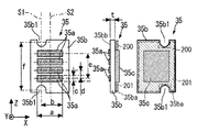
図18は、IDチップ35を示す3面図である。
図18に示すように、IDチップ35における基板35bの第1平面(オモテ面35bb)には、4つの金属板としての金属パット35aがZ方向に並設されている。この金属パット35aは、基板35b側から銅層、ニッケル層、金層の3層からなる多層構造体であって、表層となる金層は比較的高価であるものの酸化防止のため設けられている。また、金属パット35aは、予めマスキングした基板35b上への電界蒸着によって形成されたものである。
位置決め用の切欠部35b1は、4つの金属パット35aを挟むように4つの金属パット35aの配列方向(Z方向)の両端部にそれぞれ形成されている。切欠部35b1の中心を通り複数の金属パット35aの配列方向に対して平行となる第1の仮想直線S1が、複数の金属パット35aにおける長手方向の中心を結ぶ第2の仮想直線S2に対して、重ならない位置にあるように構成されている。詳しくは2つの位置決め用の切欠部35b1を結ぶ第1の仮想直線S1が、複数の金属パット35aにおける長手方向の中心を結ぶ第2の仮想直線S2に対して、重ならない位置にあるように構成されている。換言すると、切欠部35b1において基板35bの内側に向けて最も食い込んでいる部分をつないだ仮想直線S1が、仮想直線S2に対して重ならない位置にあるように構成されている。さらには、仮想直線S1は、仮想直線S2に対して略平行となるように構成されている。
FIG. 18 is a three-side view showing the ID chip 35.
As shown in FIG. 18, on the first plane (front surface 35bb) of the substrate 35b in the ID chip 35, four metal pads 35a as metal plates are arranged in parallel in the Z direction. The metal pad 35a is a multilayer structure composed of a copper layer, a nickel layer, and a gold layer from the substrate 35b side, and the gold layer as the surface layer is provided for the purpose of preventing oxidation, although it is relatively expensive. . Further, the metal pad 35a is formed by electric field vapor deposition on the substrate 35b masked in advance.
The positioning notches 35b1 are formed at both ends in the arrangement direction (Z direction) of the four metal pads 35a so as to sandwich the four metal pads 35a. The first virtual straight line S1 passing through the center of the notch 35b1 and parallel to the arrangement direction of the plurality of metal pads 35a is connected to the second virtual straight line S2 that connects the longitudinal centers of the plurality of metal pads 35a. , Is configured to be in a position that does not overlap. Specifically, the first virtual straight line S1 connecting the two positioning cutouts 35b1 is configured so as not to overlap the second virtual straight line S2 connecting the longitudinal centers of the plurality of metal pads 35a. Has been. In other words, the imaginary straight line S1 that connects the portions of the cutout 35b1 that are most biting inward toward the inside of the substrate 35b is configured so as not to overlap the imaginary straight line S2. Further, the virtual straight line S1 is configured to be substantially parallel to the virtual straight line S2.
本実施の形態1では、図18における寸法a〜fが、それぞれ、6.2mm、5.2mm、1.5mm、2mm、6mm、11.7mmに設定されている。このように小面積の基板35bは、万一外力が加わったとしても絶対的な撓み量が小さく、せん断力に対する耐性(剛性)が比較的大きくなる。本実施の形態1では、IDチップ35を保持部材34kの内部で移動可能に保持して、大面積のIDチップ35であれば切欠部35b1への位置決めピン73e3の挿入によって「こじり」を発生させるおそれがある位置決め方式を採用している。「こじり」とは切欠部35b1に対して位置決めピン73e3が垂直でなく斜めに入り、切欠部35b1と本体側突起部73e3の両者の摺動負荷が上がって基板35bが撓んで移動しなくなる状態である。しかし本実施の形態1では、上述したように基板35bが小面積である点をうまく利用して剛性を上げ、「こじり」の原因となるたわみが生じにくい位置決め方式を成立させている。また、基板35bにおける金属パット35a同士の間隔が狭小であるものの、基板35bのXZ平面内の移動にともなう高精度の位置決めにより、金属パット35aと本体側端子73e2との接触不良を抑止することができる。このため、金層を含む高価な金属パット35aの面積を極小に抑えることができている。
In the first embodiment, dimensions a to f in FIG. 18 are set to 6.2 mm, 5.2 mm, 1.5 mm, 2 mm, 6 mm, and 11.7 mm, respectively. As described above, the substrate 35b having a small area has a small absolute deflection amount even if an external force is applied, and has a relatively high resistance (rigidity) to the shearing force. In the first embodiment, the ID chip 35 is movably held inside the holding member 34k, and if the ID chip 35 has a large area, the "pick" is generated by inserting the positioning pin 73e3 into the notch 35b1. Uses a positioning method that may cause a problem. “Squeeze” is a state in which the positioning pin 73e3 is not perpendicular to the notch 35b1, but enters the slant, the sliding load of both the notch 35b1 and the main body side protrusion 73e3 increases, and the substrate 35b is bent and stops moving. is there. However, in the first embodiment, as described above, the positioning method is established in which the substrate 35b has a small area and the rigidity is increased to prevent the occurrence of the bending that causes the "twisting". Moreover, although the space | interval of the metal pads 35a in the board | substrate 35b is narrow, the contact failure with the metal pad 35a and the main body side terminal 73e2 can be suppressed by the highly accurate positioning accompanying the movement in the XZ plane of the board | substrate 35b. it can. For this reason, the area of the expensive metal pad 35a including the gold layer can be minimized.
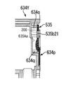
図16に示すように、IDチップ35の基板35bにおける、本体側端子73eと接触する面となるオモテ面35bbと反対側で、保持部材34kの内壁34k5との間には、低摩擦構造としての摺動向上部材200が配置されている。つまり、摺動向上部材200は、IDチップ35(基板35b)と保持部材34kとの接触領域に設けられている。摺動向上部材200は、内壁34k5と基板35bとの摺動性を良くするために、摺動性や耐摩耗性が高く、摩擦係数が低い樹脂部材として、例えばポリエチレンテレフタラート(以下「PET」と記す)などで構成されている。本実施の形態1では図18に示すように、情報記憶部35cを除く基板35bの裏面35baに両面テープなどの粘着部材201で貼り付けられて装着されている。摺動向上部材200の厚さは、少なくとも0.1mm程度がよい。作業性を考慮すると、0.1mmよりも厚い方がよく、少なくとも0.2mm程度が好ましい。
このようにIDチップ35(基板35b)と内壁34k5の間に摺動向上部材200を配することで、IDチップ35(基板35b)と内壁34k5との接触抵抗が低減して摺動性が向上する。このため、本体側突起部73e3が基板35bの切欠部35b1で案内されて移動する際に、本体側突起部73e3と基板35bの切欠部35b1とが引っかかることを防止できる。また、トナー容器32Yを画像形成装置本体100に対して正しくセットすることができ、通信不良の発生を防止することができる。
As shown in FIG. 16, the low friction structure between the inner wall 34k5 of the holding member 34k on the opposite side to the front surface 35bb that is a surface in contact with the main body side terminal 73e in the substrate 35b of the ID chip 35 is provided. A sliding improvement member 200 is disposed. That is, the sliding improvement member 200 is provided in a contact area between the ID chip 35 (substrate 35b) and the holding member 34k. The sliding improvement member 200 is, for example, polyethylene terephthalate (hereinafter referred to as “PET”) as a resin member having a high sliding property and wear resistance and a low friction coefficient in order to improve the sliding property between the inner wall 34k5 and the substrate 35b. Etc.). In the first embodiment, as shown in FIG. 18, it is attached to the back surface 35ba of the substrate 35b excluding the information storage unit 35c by being attached with an adhesive member 201 such as a double-sided tape. The thickness of the sliding improvement member 200 is preferably at least about 0.1 mm. In consideration of workability, the thickness is preferably thicker than 0.1 mm, and preferably at least about 0.2 mm.
Thus, by arranging the slide improving member 200 between the ID chip 35 (substrate 35b) and the inner wall 34k5, the contact resistance between the ID chip 35 (substrate 35b) and the inner wall 34k5 is reduced, and the slidability is improved. To do. For this reason, when the main body side protrusion 73e3 is guided and moved by the notch 35b1 of the substrate 35b, it is possible to prevent the main body side protrusion 73e3 and the notch 35b1 of the substrate 35b from being caught. Further, the toner container 32Y can be correctly set with respect to the image forming apparatus main body 100, and the occurrence of communication failure can be prevented.
図11は、画像形成装置本体100側のコネクタ73eを示す概略斜視図である。
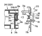
図11を参照して、コネクタ73eにおける4つの本体側端子73e2は、板状(又は線状)の金属部材であって、その一端側を固定端として他端側を自由端としてコネクタ本体73e1に固定支持されている。また、4つの本体側端子73e2は、その他端側にIDチップ35(トナー容器32Y)の側に向けて湾曲した湾曲部が形成されている。すなわち、本体側端子73e2は、IDチップ35に向けて、くの字状に屈曲している。この本体側端子73e2の湾曲部は、金属パット35aとの接点となる部分である。
そして、キャップ受部73へのキャップ部34Y(トナー容器32Y)の装着動作に伴い、まず、本体側端子73e2の湾曲部が金属パット35aの長手方向略中央部に接触する。そして、キャップ部34Yの装着動作がさらに進むと、IDチップ35(基板35b)がさらにコネクタ73e側に近づく。続いて本体側端子73e2が金属パット35aに押圧されて弾性変形(曲がっていたくの字が伸びるような状態である)しながら本体側端子73e2の湾曲部が第1の仮想直線S1に近づくように変位する。すなわち、キャップ部34Yの装着動作に伴い、本体側端子73e2の湾曲部は、金属パット35aに対する接触圧を徐々に強めながら、長手方向中央部から図18の左方(第1の仮想直線S1近傍である。)に向けてスライドすることになる。
FIG. 11 is a schematic perspective view showing the connector 73e on the image forming apparatus main body 100 side.
Referring to FIG. 11, the four main body side terminals 73e2 in the connector 73e are plate-shaped (or linear) metal members, and one end side thereof is a fixed end and the other end side is a free end to the connector main body 73e1. Fixedly supported. Further, the four main body side terminals 73e2 are formed with curved portions that are curved toward the ID chip 35 (toner container 32Y) on the other end side. That is, the main body side terminal 73e2 is bent in a dogleg shape toward the ID chip 35. The curved portion of the main body side terminal 73e2 is a portion that becomes a contact point with the metal pad 35a.
As the cap portion 34Y (toner container 32Y) is attached to the cap receiving portion 73, first, the curved portion of the main body side terminal 73e2 comes into contact with the substantially central portion in the longitudinal direction of the metal pad 35a. When the mounting operation of the cap portion 34Y further proceeds, the ID chip 35 (substrate 35b) further approaches the connector 73e side. Subsequently, the curved portion of the main body side terminal 73e2 approaches the first virtual straight line S1 while the main body side terminal 73e2 is pressed by the metal pad 35a and is elastically deformed (a state in which the bent character is extended). Displace. That is, with the mounting operation of the cap portion 34Y, the curved portion of the main body side terminal 73e2 gradually increases the contact pressure with respect to the metal pad 35a, while the left side of FIG. 18 (near the first virtual straight line S1) It will slide towards.
このような構成により、関連部品の寸法精度や組み付け精度のばらつきにより本体側端子73e2に対する金属パット35aの長手方向(Y方向)の位置がずれてしまっても、本体側端子73e2と金属パット35aとの接触不良を確実に抑止することができる。さらに、最終的に本体側端子73e2と金属パット35aとは、位置決めピン73e3と切欠部35b1とが係合する位置の近傍(第1の仮想直線S1の近傍である)で接触するため、位置決め部から接触部までの水平方向の距離を縮めることができる。その結果、本体側端子73e2と金属パット35aとの接触位置の精度が高められることになる。
With such a configuration, even if the position of the metal pad 35a in the longitudinal direction (Y direction) with respect to the main body side terminal 73e2 is shifted due to variations in dimensional accuracy and assembly accuracy of related parts, the main body side terminal 73e2 and the metal pad 35a It is possible to reliably prevent contact failure. Furthermore, since the main body side terminal 73e2 and the metal pad 35a finally come into contact with each other in the vicinity of the position where the positioning pin 73e3 and the notch 35b1 engage (the vicinity of the first virtual straight line S1), the positioning portion The horizontal distance from the contact portion to the contact portion can be reduced. As a result, the accuracy of the contact position between the main body side terminal 73e2 and the metal pad 35a is improved.
本実施の形態1では、複数の金属パット35aの配列方向が鉛直方向(Z方向)になるように並設されている。これにより、キャップ受部73におけるキャップ部34Yの位置決め方向と、コネクタ73eと基板35bとの位置決め方向とが同一方向になる。すなわち、位置決めピン73a、73bや位置決め穴部34a、34bの配列方向と、位置決めピン73e3や切欠部35b1の配列方向とが同一方向になる。このため、本体側端子73e2と金属パット35aとの接触不良がより生じ難くなる。
In the first embodiment, the plurality of metal pads 35a are arranged side by side so that the arrangement direction is the vertical direction (Z direction). Thereby, the positioning direction of the cap part 34Y in the cap receiving part 73 and the positioning direction of the connector 73e and the board | substrate 35b become the same direction. That is, the arrangement direction of the positioning pins 73a and 73b and the positioning holes 34a and 34b and the arrangement direction of the positioning pins 73e3 and the notch 35b1 are the same direction. For this reason, poor contact between the main body side terminal 73e2 and the metal pad 35a is less likely to occur.
図15を参照して、キャップ部34Yの位置決め穴部34a、34bは、IDチップ35を挟むように鉛直方向の離れた位置にそれぞれ形成されている。位置決め穴部34a、34bは、2つの位置決め穴部34a、34bの中心を結ぶ第3の仮想直線S3が、図18に示した2つの位置決め用の切欠部35b1を結ぶ第1の仮想直線S1に対して平行になるように構成されている。
このように、IDチップ35が第1の位置決め穴部34a(主基準)と第2の位置決め穴部34b(従基準)との間に固設されているために、キャップ受部73のコネクタ73eに対してIDチップ35の位置が高精度に定められることになる。したがって、コネクタ73eに対するIDチップ35の位置ずれによる通信不良を抑止することができる。また、キャップ受部73におけるキャップ部34Yの位置決め方向と、コネクタ73eと基板35bとの位置決め方向とが同一方向になる。すなわち、位置決めピン73a、73bや位置決め穴部34a、34bの配列方向と、位置決めピン73e3や切欠部35b1の配列方向とが同一方向になる。このため、トナー容器32Yの画像形成装置本体100への位置決め動作が、コネクタ73eに対する基板35bの位置決めをしやすい方向に寄与する。その結果、本体側端子73e2と金属パット35aとの接触不良が生じ難くなる効果がさらに大きくなる。
Referring to FIG. 15, the positioning holes 34 a and 34 b of the cap part 34 </ b> Y are formed at positions separated in the vertical direction so as to sandwich the ID chip 35. In the positioning holes 34a and 34b, the third virtual straight line S3 that connects the centers of the two positioning holes 34a and 34b becomes the first virtual straight line S1 that connects the two positioning notches 35b1 shown in FIG. It is comprised so that it may become parallel with respect to.
Thus, since the ID chip 35 is fixed between the first positioning hole 34a (main reference) and the second positioning hole 34b (secondary reference), the connector 73e of the cap receiving portion 73 is provided. On the other hand, the position of the ID chip 35 is determined with high accuracy. Therefore, it is possible to suppress a communication failure due to the displacement of the ID chip 35 with respect to the connector 73e. Moreover, the positioning direction of the cap part 34Y in the cap receiving part 73 and the positioning direction of the connector 73e and the board | substrate 35b become the same direction. That is, the arrangement direction of the positioning pins 73a and 73b and the positioning holes 34a and 34b and the arrangement direction of the positioning pins 73e3 and the notch 35b1 are the same direction. Therefore, the positioning operation of the toner container 32Y with respect to the image forming apparatus main body 100 contributes to the direction in which the substrate 35b can be easily positioned with respect to the connector 73e. As a result, the effect that the contact failure between the main body side terminal 73e2 and the metal pad 35a is less likely to occur is further increased.
本実施の形態1では、接触式のIDチップ35が、本体側端子73e2に対して金属パット35aが近づいて接触するときの移動方向に対して略直交する仮想平面上を移動できるように、保持部材34kに保持されている。このため、画像形成装置本体100に対して着脱可能に設置されるトナー容器32Yに、IDチップ35を設置した場合でも、画像形成装置本体100のコネクタ73eの本体側端子73e2との位置決め不良による接触不良が生じ難くなる。
また、IDチップ35(基板35b)と内壁34k5の間に摺動向上部材200を配置している。このため、IDチップ35(基板35b)と内壁34k5との接触抵抗が低減して摺動性が向上し、本体側突起部73e3が基板35bの切欠部35b1で案内されて移動する際に、本体側突起部73e3と基板35bの切欠部35b1とが引っかかることを防止できる。その結果、トナー容器32Yを画像形成装置本体100に対して正しくセットすることができ、通信不良の発生をより確実に防止することができる。
In the first embodiment, the contact-type ID chip 35 is held so that it can move on a virtual plane substantially orthogonal to the moving direction when the metal pad 35a approaches and comes into contact with the main body side terminal 73e2. It is held by the member 34k. Therefore, even when the ID chip 35 is installed in the toner container 32Y that is detachably installed on the image forming apparatus main body 100, contact due to poor positioning with the main body side terminal 73e2 of the connector 73e of the image forming apparatus main body 100. Defects are difficult to occur.
Further, the sliding improvement member 200 is disposed between the ID chip 35 (substrate 35b) and the inner wall 34k5. For this reason, the contact resistance between the ID chip 35 (substrate 35b) and the inner wall 34k5 is reduced and the slidability is improved, and the main body side protrusion 73e3 is guided by the notch 35b1 of the substrate 35b and moves. It is possible to prevent the side protrusion 73e3 and the notch 35b1 of the substrate 35b from being caught. As a result, the toner container 32Y can be correctly set with respect to the image forming apparatus main body 100, and the occurrence of poor communication can be more reliably prevented.
実施の形態2
図19〜図21にて、本発明の実施の形態2について詳細に説明する。
図19は、実施の形態2におけるトナー容器232Yを示す概略断面図である。図20は、トナー容器232Yにおけるキャップ部234Yを示す背面図である。また、図21は、保持部材234kに嵌合する保持蓋234k8を示す斜視図である。本実施の形態2におけるトナー容器232Yは、情報記憶装置を保持する保持部としての保持部材234kの構成が、前記実施の形態1のものと相違する。
Embodiment 2
The second embodiment of the present invention will be described in detail with reference to FIGS.
FIG. 19 is a schematic cross-sectional view showing the toner container 232Y in the second embodiment. FIG. 20 is a rear view showing the cap portion 234Y in the toner container 232Y. FIG. 21 is a perspective view showing a holding lid 234k8 fitted to the holding member 234k. The toner container 232Y according to the second embodiment is different from that according to the first embodiment in the configuration of the holding member 234k as a holding unit that holds the information storage device.
本実施の形態2におけるトナー容器232Yも、実施の形態1のものと同様に、容器本体33Yとキャップ部234Yとで構成されている。そして、キャップ部234Yには、情報記憶装置としてのIDチップ35が着脱可能に設置されている。ここで、本実施の形態2におけるキャップ部234Yは、IDチップ35の一部(金属パット35aと切欠部35b1とである)が露呈する開口34k2が形成された保持部材234kが、一体的に形成されている。そして、IDチップ35は、キャップ部234Yの内側から図19の白矢印方向に挿入されて保持部材234kの位置にセットされる。そして、保持部材234kの位置にIDチップ35がセットされた状態で、キャップ部234Yの内側から図191の白矢印方向に保持蓋234k8が挿入されて保持部材234kに嵌合される(図20の状態である)。
Similarly to the first embodiment, the toner container 232Y according to the second embodiment also includes a container body 33Y and a cap portion 234Y. An ID chip 35 as an information storage device is detachably installed on the cap portion 234Y. Here, the cap member 234Y in the second embodiment is integrally formed with a holding member 234k formed with an opening 34k2 in which a part of the ID chip 35 (the metal pad 35a and the cutout portion 35b1) is exposed. Has been. The ID chip 35 is inserted from the inside of the cap portion 234Y in the direction of the white arrow in FIG. 19 and set at the position of the holding member 234k. Then, with the ID chip 35 set at the position of the holding member 234k, the holding lid 234k8 is inserted from the inside of the cap portion 234Y in the direction of the white arrow in FIG. 191, and is fitted to the holding member 234k (FIG. 20). State).
保持蓋234k8には、図21に示すように、基板35bに接触しないように保持部材134kに嵌合するための台座部234qが設けられている。保持蓋234k8は、トナー容器232Y内のトナーが漏出してIDチップ35に付着しないように、キャップ部234Yの内壁に対して隙間なく密着するように設置される。本実施の形態2においても、保持部材234k(及び、保持蓋234k8)において、IDチップ35(基板35b)がXZ平面内を移動できるように保持されている。無論、本実施の形態2においても、図19に示すように、内壁34k5と対向するIDチップ35の基板35bの裏面側35baには、摺動向上部材200を配置している。
As shown in FIG. 21, the holding lid 234k8 is provided with a pedestal portion 234q for fitting into the holding member 134k so as not to contact the substrate 35b. The holding lid 234k8 is installed so that the toner in the toner container 232Y does not leak and adhere to the ID chip 35 so as to be in close contact with the inner wall of the cap portion 234Y. Also in the second embodiment, the ID chip 35 (substrate 35b) is held by the holding member 234k (and the holding lid 234k8) so that it can move in the XZ plane. Of course, also in the second embodiment, as shown in FIG. 19, the slide improving member 200 is disposed on the back surface side 35ba of the substrate 35b of the ID chip 35 facing the inner wall 34k5.
本実施の形態2では、実施の形態1と同様に、接触式のIDチップ35が、本体側端子73e2に対して金属パット35aが近づいて接触するときの移動方向に対して略直交する仮想平面上を移動できるように保持部材234kに保持されている。これにより、画像形成装置本体100に対して着脱可能に設置されるトナー容器232Yに、IDチップ35を設置した場合でも、画像形成装置本体100のコネクタ73eの本体側端子73e2との位置決め不良による接触不良が生じ難くなる。
また、IDチップ35(基板35b)と内壁34k5の間に摺動向上部材200を配置している。このため、IDチップ35(基板35b)と内壁34k5との接触抵抗が低減して摺動性が向上し、本体側突起部73e3が基板35bの切欠部35b1で案内されて移動する際に、本体側突起部73e3と基板35bの切欠部35b1とが引っかかることを防止でき。その結果、トナー容器32Yを画像形成装置本体100に対して正しくセットすることができ、通信不良の発生をより確実に防止することができる。
In the second embodiment, similarly to the first embodiment, the contact-type ID chip 35 is a virtual plane that is substantially orthogonal to the moving direction when the metal pad 35a approaches and comes into contact with the main body side terminal 73e2. It is held by a holding member 234k so that it can move upward. Accordingly, even when the ID chip 35 is installed in the toner container 232Y that is detachably installed on the image forming apparatus main body 100, contact due to poor positioning with the main body side terminal 73e2 of the connector 73e of the image forming apparatus main body 100. Defects are less likely to occur.
Further, the sliding improvement member 200 is disposed between the ID chip 35 (substrate 35b) and the inner wall 34k5. For this reason, the contact resistance between the ID chip 35 (substrate 35b) and the inner wall 34k5 is reduced and the slidability is improved, and the main body side protrusion 73e3 is guided by the notch 35b1 of the substrate 35b and moves. It is possible to prevent the side protrusion 73e3 and the notch 35b1 of the substrate 35b from being caught. As a result, the toner container 32Y can be correctly set with respect to the image forming apparatus main body 100, and the occurrence of poor communication can be more reliably prevented.
実施の形態3.
図22にて、本発明の実施の形態3について詳細に説明する。
図22は、実施の形態3におけるトナー容器332YのIDチップ35(情報記憶装置)がキャップ受部73のコネクタ73eにセットされる状態を示す模式図であって、実施の形態1における図16に相当する図である。
本実施の形態3は、保持部材34kの内部にクッション材334k10が設置されている点と、キャップ受部373における壁部373gの構成とが実施の形態1と相違している。
Embodiment 3 FIG.
The third embodiment of the present invention will be described in detail with reference to FIG.
FIG. 22 is a schematic diagram illustrating a state where the ID chip 35 (information storage device) of the toner container 332Y according to the third embodiment is set in the connector 73e of the cap receiving portion 73. FIG. It is an equivalent figure.
The third embodiment is different from the first embodiment in that the cushion material 334k10 is installed inside the holding member 34k and the configuration of the wall portion 373g in the cap receiving portion 373.
本実施の形態3におけるトナー容器332Yも、各実施の形態のものと同様に、容器本体33Yとキャップ部34Yとで構成されている。そして、キャップ部34Yには、情報記憶装置としてのIDチップ35が着脱可能に設置されている。さらに、保持部材34kの内部において、IDチップ35がXZ平面内を移動できるように保持されている。
The toner container 332Y according to the third embodiment is also composed of a container main body 33Y and a cap portion 34Y as in the case of the respective embodiments. An ID chip 35 as an information storage device is detachably installed on the cap portion 34Y. Further, the ID chip 35 is held inside the holding member 34k so as to be movable in the XZ plane.
ここで、本実施の形態3では、保持部材34kの内壁34k5と基板35bとの間にクッション材334k10が設けられている。このクッション材334k10は、発泡ポリウレタン等の弾性材料からなり、基板35bの裏面35baに装着されている。これにより、IDチップ(基板35b)のXZ平面内の移動を妨げることなく、位置決めピン73e3が切欠部35b1に係合するときに基板35bに生じるダメージを軽減することができる。
本形態において、クッション材334k10と内壁34k5の間には摺動向上部材200を配置している。本形態では、摺動向上部材200をクッション材334k10側に両面テープなどの粘着部材201により貼り付けて配置している。
Here, in the third embodiment, the cushion material 334k10 is provided between the inner wall 34k5 of the holding member 34k and the substrate 35b. The cushion material 334k10 is made of an elastic material such as polyurethane foam, and is attached to the back surface 35ba of the substrate 35b. Thereby, the damage which arises in the board | substrate 35b when the positioning pin 73e3 engages with the notch part 35b1 can be reduced, without preventing the movement in the XZ plane of ID chip (board | substrate 35b).
In this embodiment, the sliding improvement member 200 is disposed between the cushion material 334k10 and the inner wall 34k5. In the present embodiment, the sliding improvement member 200 is disposed on the cushion material 334k10 side by being attached with an adhesive member 201 such as a double-sided tape.
本実施の形態3では、キャップ受部373における壁部373gが、コネクタ73gの四方を囲むように設置されている。そして、これに対応するように、キャップ部34Yには、壁部373gとの干渉を避けるための凹部が設けられている。このように、壁部373gを設けることで、トナー容器332Yのトナー排出口Wの近傍から外部にトナーが飛散してしまっても、コネクタ73eやIDチップ35に飛散トナーが直接的に付着し難くなる。したがって、飛散トナーによるコネクタ73e(本体側端子73e2)とIDチップ35(金属パット35a)との接触不良(通信不良)を抑止することができる。
In the third embodiment, the wall portion 373g of the cap receiving portion 373 is installed so as to surround the four sides of the connector 73g. And corresponding to this, the cap part 34Y is provided with the recessed part for avoiding interference with the wall part 373g. As described above, by providing the wall portion 373g, even when the toner scatters from the vicinity of the toner discharge port W of the toner container 332Y, the scattered toner hardly adheres directly to the connector 73e or the ID chip 35. Become. Therefore, contact failure (communication failure) between the connector 73e (main body side terminal 73e2) and the ID chip 35 (metal pad 35a) due to scattered toner can be suppressed.
本実施の形態3においても、各実施の形態と同様に、接触式のIDチップ35が、本体側端子73e2に対して金属パット35aが近づいて接触するときの移動方向に対して略直交する仮想平面上を移動できるように保持部材34kに保持されている。これにより、画像形成装置本体100に対して着脱可能に設置されるトナー容器332Yに、IDチップ35を設置した場合でも、画像形成装置本体100のコネクタ73eの本体側端子73e2との位置決め不良による接触不良が生じ難くなる。
また、基板35bの裏面35baに設けたクッション材334k10と内壁34k5の間に摺動向上部材200を配置している。このため、IDチップ35(基板35b)と内壁34k5との接触抵抗が低減して摺動性が向上し、本体側突起部73e3が基板35bの切欠部35b1で案内されて移動する際に、本体側突起部73e3と基板35bの切欠部35b1とが引っかかることを防止できる。その結果、トナー容器32Yを画像形成装置本体100に対して正しくセットすることができ、通信不良の発生をより確実に防止することができる。
Also in the third embodiment, similarly to each embodiment, the contact type ID chip 35 is virtually orthogonal to the moving direction when the metal pad 35a approaches and comes into contact with the main body side terminal 73e2. It is held by a holding member 34k so that it can move on a plane. Thus, even when the ID chip 35 is installed in the toner container 332Y that is detachably installed on the image forming apparatus main body 100, contact due to poor positioning with the main body side terminal 73e2 of the connector 73e of the image forming apparatus main body 100. Defects are less likely to occur.
Moreover, the sliding improvement member 200 is arrange | positioned between the cushion material 334k10 provided in the back surface 35ba of the board | substrate 35b, and the inner wall 34k5. For this reason, the contact resistance between the ID chip 35 (substrate 35b) and the inner wall 34k5 is reduced and the slidability is improved, and the main body side protrusion 73e3 is guided by the notch 35b1 of the substrate 35b and moves. It is possible to prevent the side protrusion 73e3 and the notch 35b1 of the substrate 35b from being caught. As a result, the toner container 32Y can be correctly set with respect to the image forming apparatus main body 100, and the occurrence of poor communication can be more reliably prevented.
実施の形態4.
図23にて、この発明の実施の形態4について詳細に説明する。
図23は、実施の形態4における情報記憶装置となるIDチップ435の基板435bを示す3面図であって、前記実施の形態1における図9に相当する図である。
Embodiment 4 FIG.
A fourth embodiment of the present invention will be described in detail with reference to FIG.
FIG. 23 is a trihedral view showing the substrate 435b of the ID chip 435 serving as the information storage device in the fourth embodiment, and corresponds to FIG. 9 in the first embodiment.
本実施の形態4におけるトナー容器(432Y)も、前記各実施の形態のものと同様に、容器本体33Yとキャップ部34Yとで構成されている。そして、キャップ部34Yには、情報記憶装置としてのIDチップ435が着脱可能に設置されている。さらに、保持部材34kの内部において、IDチップ435がXZ平面内を移動できるように保持されている。
The toner container (432Y) in the fourth embodiment is also composed of a container main body 33Y and a cap portion 34Y, as in the above-described embodiments. An ID chip 435 as an information storage device is detachably installed on the cap part 34Y. Further, the ID chip 435 is held inside the holding member 34k so as to be movable in the XZ plane.
本実施の形態4におけるIDチップ435の基板435bには、前記各実施の形態における位置決め用の切欠部35b1の代わりに、ガイド部として位置決め用の穴部435b11、435b12が基板435bを貫通して設けられている。そして、トナー容器(432Y)の装着動作に伴い、基板435bがXZ平面内を自由に移動しながら、コネクタ73eの位置決めピン73e3に対して位置決め用の穴部435b11、435b12が係合して挿入することになる。詳しくは、穴部435b11、435b12の縁部(又は、内面)に位置決めピン73e3が接触して、基板435bの動きが規制されることになる。これにより、複数の金属パット35aと、コネクタ73eの本体側端子73e2との位置決め不良による接触不良が生じ難くなる。本形態では、基板435bの裏面435baに摺動向上部材200を粘着部材201により貼り付けて配置している。
In the substrate 435b of the ID chip 435 according to the fourth embodiment, positioning holes 435b11 and 435b12 are provided through the substrate 435b as guide portions instead of the positioning notches 35b1 according to the respective embodiments. It has been. Then, as the toner container (432Y) is mounted, the positioning holes 435b11 and 435b12 are engaged with and inserted into the positioning pins 73e3 of the connector 73e while the substrate 435b freely moves in the XZ plane. It will be. Specifically, the positioning pin 73e3 comes into contact with the edge (or the inner surface) of the holes 435b11 and 435b12, and the movement of the substrate 435b is restricted. This makes it difficult for poor contact due to poor positioning between the plurality of metal pads 35a and the main body side terminal 73e2 of the connector 73e. In this embodiment, the sliding improvement member 200 is attached to the back surface 435ba of the substrate 435b with the adhesive member 201 and disposed.
本実施の形態4では、基板435bの下方に円形の位置決め用の穴部435b11を形成し、基板435bの上方に長穴形状の位置決め用の穴部435b12を形成している。これは、位置決め用の穴部435b11、435b12が位置決めピン73e3に係合する直前まで、基板435b自体の重量によって保持部材34k内において基板435bが下方に位置していることを考慮したためである。下方の穴部435b11が位置決めピン73e3に拾われることで基板435bが持ち上がり、もう一方の長穴(穴部435b12)にもスムーズに位置決めピン73e3が挿入される。仮に下方の穴部が長穴であって上方の穴部が丸穴の場合には、位置決めピン73e3で基板435bを持ち上げることができずに、上方の丸穴に位置決めピン73e3が挿入し難くなるおそれがある。
In the fourth embodiment, a circular positioning hole 435b11 is formed below the substrate 435b, and a long hole-shaped positioning hole 435b12 is formed above the substrate 435b. This is because the substrate 435b is positioned below in the holding member 34k by the weight of the substrate 435b until just before the positioning holes 435b11 and 435b12 engage with the positioning pin 73e3. When the lower hole 435b11 is picked up by the positioning pin 73e3, the substrate 435b is lifted, and the positioning pin 73e3 is smoothly inserted into the other long hole (hole 435b12). If the lower hole is a long hole and the upper hole is a round hole, the substrate 435b cannot be lifted by the positioning pin 73e3, and the positioning pin 73e3 is difficult to insert into the upper round hole. There is a fear.
本実施の形態4では、IDチップ435の基板435bにおいて、2つの位置決め用の穴部435b11、435b12を形成した。これに対して、IDチップ435の基板435bにおいて、一方を位置決め用の穴部435b11(又は、435b12)として、他方を位置決め用の切欠部35b1(前記各実施の形態で用いられたものである)とすることもできる。そして、そのような場合でも、本実施の形態4と同様の効果を得ることができる。
In the fourth embodiment, two positioning holes 435b11 and 435b12 are formed in the substrate 435b of the ID chip 435. On the other hand, in the substrate 435b of the ID chip 435, one is used as a positioning hole 435b11 (or 435b12) and the other is used as a positioning notch 35b1 (used in each of the above embodiments). It can also be. Even in such a case, the same effect as in the fourth embodiment can be obtained.
本実施の形態4においても、各実施の形態と同様に、接触式のIDチップ435が、本体側端子73e2に対して金属パット35aが近づいて接触するときの移動方向に対して略直交する仮想平面上を移動できるように保持部材34kに保持されている。これにより、画像形成装置本体100に対して着脱可能に設置されるトナー容器に、IDチップ435を設置した場合でも、画像形成装置本体100のコネクタ73eの本体側端子73e2との位置決め不良による接触不良が生じ難くなる。
下方の位置決め用の穴部435b11が位置決めピン73e3に拾われて案内されて基板435bが持ち上がって移動し、もう一方の長穴(位置決め用の穴部435b12)に位置決めピン73e3が案内されて挿入される。この際、基板435bの裏面435baに摺動向上部材200を配置しているので、IDチップ435(基板435b)と内壁34k5との接触抵抗が低減して摺動性が向上する。このため、本体側突起部73e3と基板435bの各穴部435b11、穴部435b12とが引っかかることや噛み込むのを防止できる。その結果、トナー容器32Yを画像形成装置本体100に対して正しくセットすることができ、通信不良の発生をより確実に防止することができる。
Also in the fourth embodiment, as in each embodiment, the contact-type ID chip 435 is virtually orthogonal to the moving direction when the metal pad 35a approaches and comes into contact with the main body side terminal 73e2. It is held by a holding member 34k so that it can move on a plane. Thereby, even when the ID chip 435 is installed in a toner container that is detachably installed on the image forming apparatus main body 100, poor contact due to poor positioning with the main body side terminal 73e2 of the connector 73e of the image forming apparatus main body 100. Is less likely to occur.
The lower positioning hole 435b11 is picked up and guided by the positioning pin 73e3, the substrate 435b is lifted and moved, and the positioning pin 73e3 is guided and inserted into the other long hole (positioning hole 435b12). The At this time, since the slide improving member 200 is disposed on the back surface 435ba of the substrate 435b, the contact resistance between the ID chip 435 (substrate 435b) and the inner wall 34k5 is reduced, and the slidability is improved. For this reason, it can prevent that the main body side protrusion part 73e3, each hole part 435b11 of the board | substrate 435b, and the hole part 435b12 catch or bite. As a result, the toner container 32Y can be correctly set with respect to the image forming apparatus main body 100, and the occurrence of poor communication can be more reliably prevented.
実施の形態5.
図23〜図29にて、本発明の実施の形態5について詳細に説明する。
図23は、実施の形態5における情報記憶装置となるIDチップ535の基板535bを示す3面図であって、前記実施の形態1における図18に相当する図である。図25は、IDチップ535と保持部材534k(534k25)とコネクタ573eとを示す斜視図であって、3つの部材534k(534k25)、535、573eの相対位置関係を示す斜視図である。図26は、IDチップ535がコネクタ573eに係合した状態を示す斜視図である。また、図27は、IDチップ535の電気回路とコネクタ573eの電気回路とを示す回路図である。図28(A)はIDチップ535がコネクタ573eに保持された状態を示す正面図であって、図28(B)はIDチップ535がガイド部となる位置決め用の穴部535b21を中心に回転している状態を示す正面図である。図29は、工場製造時の検査工程においてプローブ端子401が当接された状態のIDチップ535を示す図である。
本実施の形態5では、IDチップ535の基板535bに位置決め用の穴部535b21が1つだけ形成されている。本実施の形態5では、位置決め用の穴部535b21が複数の矩形状の金属パット35a1、35a2、35a3(金属板)の間に配置されている。この二点が前記各実施の形態と相違している。
Embodiment 5. FIG.
A fifth embodiment of the present invention will be described in detail with reference to FIGS.
FIG. 23 is a trihedral view showing the substrate 535b of the ID chip 535 serving as the information storage device in the fifth embodiment, and corresponds to FIG. 18 in the first embodiment. FIG. 25 is a perspective view showing the ID chip 535, the holding member 534k (534k25), and the connector 573e, and is a perspective view showing the relative positional relationship between the three members 534k (534k25), 535, and 573e. FIG. 26 is a perspective view showing a state where the ID chip 535 is engaged with the connector 573e. FIG. 27 is a circuit diagram showing an electric circuit of the ID chip 535 and an electric circuit of the connector 573e. FIG. 28A is a front view showing a state in which the ID chip 535 is held by the connector 573e. FIG. 28B is a view in which the ID chip 535 rotates around a positioning hole 535b21 serving as a guide portion. It is a front view showing a state. FIG. 29 is a diagram showing the ID chip 535 in a state in which the probe terminal 401 is in contact in the inspection process at the time of factory manufacture.
In the fifth embodiment, only one positioning hole 535b21 is formed in the substrate 535b of the ID chip 535. In the fifth embodiment, the positioning hole 535b21 is disposed between a plurality of rectangular metal pads 35a1, 35a2, and 35a3 (metal plates). These two points are different from the above embodiments.
図24を参照して、本実施の形態5におけるIDチップ535は、基板535bの重心よりも鉛直方向上方の位置に、位置決め用の穴部535b21が基板535bを貫通するように形成されている。そして、この穴部535b21の内径部と周囲とには、接地(アース)用の金属端子535dが設置されている。本実施の形態5において、本体側端子73e2と接触する面側となる基板535bの表面535bbに形成された金属端子535dは、円環状の部分に対して2つの突出部535d1が水平方向に延設されるように形成されている。また、位置決め用の穴部535b21に対して、鉛直方向上方の位置には1つの矩形状の金属パット35a1が設置され、鉛直方向下方の位置には2つの矩形状の金属パット35a2、35a3が設置されている。
基板535bの裏面(本体側端子73e2と接触する面と反対の面)535baには、半球面状のエポキシ等の樹脂材料からなり情報記憶部35Cを覆って保護する保護部材535eが設けられている。本実施の形態5において、基板535bの形状や保護部材535eの裏面の構成・配置によるが、内部にIC等の情報記憶部35Cを有する。このこともあって、裏面535baで最も大きく重量がある構成物であるところの保護部材535eの上方に穴部535b21を配置した。このため、前述したIDチップ535の重心の鉛直上方に穴部535b21があるという位置関係を実現している。具体的には、図28(A)を参照して、本実施の形態5におけるIDチップ535は、位置決め用の穴部535b21の中心位置が、IDチップ535の重心から距離Zaだけ上方になるように形成されている。
基板535bの裏面535baには、位置決め用の穴部535b21と保護部材535eとを避けるように、摺動向上部材200を粘着部材201により貼り付けて配置している。この裏面535baは、図25に示す保持部材534kの第2対向部534k25と対向する。
Referring to FIG. 24, ID chip 535 in the fifth embodiment is formed at a position vertically above the center of gravity of substrate 535b so that positioning hole 535b21 penetrates substrate 535b. In addition, a metal terminal 535d for grounding (earth) is provided on the inner diameter portion and the periphery of the hole portion 535b21. In the fifth embodiment, the metal terminal 535d formed on the surface 535bb of the substrate 535b on the surface side in contact with the main body side terminal 73e2 has two projecting portions 535d1 extending in the horizontal direction with respect to the annular portion. It is formed to be. Further, with respect to the positioning hole 535b21, one rectangular metal pad 35a1 is installed at a position above the vertical direction, and two rectangular metal pads 35a2 and 35a3 are installed at a position below the vertical direction. Has been.
A protective member 535e made of a resin material such as a hemispherical epoxy and covering and protecting the information storage unit 35C is provided on the back surface (the surface opposite to the surface in contact with the main body side terminal 73e2) 535ba of the substrate 535b. . In the fifth embodiment, depending on the shape of the substrate 535b and the configuration and arrangement of the back surface of the protective member 535e, an information storage unit 35C such as an IC is provided inside. For this reason, the hole portion 535b21 is disposed above the protective member 535e, which is a component having the largest weight on the back surface 535ba. For this reason, the positional relationship that the hole 535b21 is vertically above the center of gravity of the ID chip 535 described above is realized. Specifically, referring to FIG. 28A, in the ID chip 535 in the fifth embodiment, the center position of the positioning hole 535b21 is above the center of gravity of the ID chip 535 by a distance Za. Is formed.
On the back surface 535ba of the substrate 535b, the sliding improvement member 200 is attached by the adhesive member 201 so as to avoid the positioning hole 535b21 and the protection member 535e. The back surface 535ba faces the second facing portion 534k25 of the holding member 534k shown in FIG.
図25を参照して、コネクタ573eは、樹脂製で中空の箱であるコネクタ本体573e21を有している。コネクタ本体573e21には1本の中空円筒で先端にテーパ形状を有する位置決めピン573e23(位置決め用の突起部)が水平方向に起立するように設けられている。そして、この位置決めピン573e23には、接地用の本体側端子573e25(アース端子)が設置されている。この接地用の本体側端子573e25は、板状(又は線状)の金属部材であって、その一部がコネクタ本体73e21と一体で形成された位置決めピン573e23の中空部に収納されている。本体側端子573e25は、その湾曲部が中空円筒の周面の一部に形成されたスリット状の開口から露出して円筒外周面から突出している。位置決めピン573e23(接地用の本体側端子573e25)に対して、鉛直方向上方の位置には1つの本体側端子73e2が設置され、鉛直方向下方の位置には2つの本体側端子73e2が設置されている。これらの本体側端子73e2は、板状(又は線状)の金属部材であって、設置位置が異なる以外は、前記各実施の形態のものとほぼ同様に形成されている。
コネクタ本体573e21の下方であって、位置決めピン573e23を挟む両側の位置には、振れ防止部材573e24が設けられている。振れ防止部材573e24は、互いの先端内側のテーパ面が線対称になるよう形成された一対のリブからなり、IDチップ535の両側端面であって穴部535b21の中心よりも鉛直下方の箇所に対向する規制部材として機能する。
Referring to FIG. 25, the connector 573e has a connector main body 573e21 that is a hollow box made of resin. The connector main body 573e21 is provided with a positioning pin 573e23 (positioning projection) having a single hollow cylinder and a tapered shape at the tip so as to stand in the horizontal direction. The positioning pin 573e23 is provided with a grounding body side terminal 573e25 (ground terminal). The grounding main body side terminal 573e25 is a plate-shaped (or linear) metal member, and a part thereof is housed in a hollow portion of a positioning pin 573e23 formed integrally with the connector main body 73e21. The main body side terminal 573e25 has a curved portion exposed from a slit-like opening formed in a part of the peripheral surface of the hollow cylinder and protruding from the outer peripheral surface of the cylinder. With respect to the positioning pin 573e23 (the main body side terminal 573e25 for grounding), one main body side terminal 73e2 is installed at a position above the vertical direction, and two main body side terminals 73e2 are installed at a position below the vertical direction. Yes. These main body side terminals 73e2 are plate-shaped (or linear) metal members, and are formed in substantially the same manner as those of the above-described embodiments except that the installation positions are different.
A shake preventing member 573e24 is provided below the connector main body 573e21 and on both sides of the positioning pin 573e23. The anti-vibration member 573e24 is formed of a pair of ribs formed so that the tapered surfaces on the inner sides of the tips are axisymmetric, and faces both ends of the ID chip 535 and vertically below the center of the hole 535b21. Functions as a regulating member.
保持部材534kは、前記各実施の形態のものと同様に、トナー容器(532Y)に固定され、コネクタ573eとIDチップ535との間に位置する。その形状は前記各実施の形態のものとほぼ同一であって、その機能(IDチップ535を、XZ平面内を移動可能に保持する機能である)も同一である。図25を参照して、本実施の形態5における保持部材534kは、第1対向部534k24が垂直方向の軸を基準に線対称に構成され、IDチップ535の上端の2つの角から穴部535e21の両側までの領域を覆うように形成されている。また、保持部材534kは、下方においても基板535bの最下段の金属パット35a3よりも下方を覆うように形成されており、これらの構成により保持部材534kからのIDチップ535の脱落を防止している。
保持部材534kにおいて、コネクタ573eの4つの本体側端子73e2、573e25に対向する領域を含む第1対向部534k24の大部分は開口となっている。特に、保持部材534kにおいて、一対の振れ防止部材573e24に対応する部分まで開放された凸型の開口534k22になっている。そして、トナー容器532Yの装着時には、位置決めピン573e23の開口534k22への侵入に続いて、振れ防止部材573e24も開口534k22を介して保持部材534kの内部に侵入することになる。
The holding member 534k is fixed to the toner container (532Y) and is located between the connector 573e and the ID chip 535, as in the above embodiments. Its shape is almost the same as that of each of the above embodiments, and its function (the function of holding the ID chip 535 movably in the XZ plane) is also the same. Referring to FIG. 25, in the holding member 534k in the fifth embodiment, the first facing portion 534k24 is configured to be line-symmetric with respect to the vertical axis, and the hole portion 535e21 is formed from two corners at the upper end of the ID chip 535. It is formed so as to cover the area up to both sides. In addition, the holding member 534k is formed so as to cover the lower side of the lowermost metal pad 35a3 of the substrate 535b even in the lower side, and by these configurations, the ID chip 535 is prevented from falling off from the holding member 534k. .
In the holding member 534k, most of the first facing portion 534k24 including an area facing the four main body side terminals 73e2 and 573e25 of the connector 573e is an opening. In particular, the holding member 534k is a convex opening 534k22 that is open to a portion corresponding to the pair of shake preventing members 573e24. When the toner container 532Y is mounted, the shake preventing member 573e24 also enters the holding member 534k through the opening 534k22 following the intrusion of the positioning pin 573e23 into the opening 534k22.
IDチップ535の裏面535ba側に対向する保持部となる平板状の第2対向部534k25は、保持部材534kに接着又は図示しないスナップフィット等で固定されている。第2対向部534k25は、第1対向部534k24と同様に、凸型の開口534k26を有し、保護部材535eや侵入してくる振れ防止部材573e24との干渉を避けることができる。その一方で、IDチップ535の穴部535b21に位置決めピン573e23が挿入されるときにIDチップ535が押されることになる。しかし、第2対向部534k25が基板535bを後ろから支えることになるため、端子同士の当接状態を維持することができる。
A flat plate-like second facing portion 534k25 serving as a holding portion facing the back surface 535ba side of the ID chip 535 is fixed to the holding member 534k by bonding or snap fitting (not shown). Similar to the first opposing portion 534k24, the second opposing portion 534k25 has a convex opening 534k26 and can avoid interference with the protective member 535e and the intrusion prevention member 573e24. On the other hand, when the positioning pin 573e23 is inserted into the hole 535b21 of the ID chip 535, the ID chip 535 is pushed. However, since the second facing portion 534k25 supports the substrate 535b from behind, the contact state between the terminals can be maintained.
図26は、実施の形態5におけるトナー容器532Yが画像形成装置本体100に装着された際に、本体側端子73e2、573e25と上述の金属パット35a1〜35a3、アース端子535dとが接続した状態を示す。この状態は、画像形成装置本体100側のコネクタ573eとIDチップ535の位置決めが完了したときの状態である。図26では、理解容易のため、コネクタ573eとIDチップ535との間にある保持部材534k(534k25)と金属パット35a1〜35a3の図示は省略されている。
FIG. 26 shows a state where the main body side terminals 73e2 and 573e25 are connected to the metal pads 35a1 to 35a3 and the ground terminal 535d when the toner container 532Y according to the fifth embodiment is attached to the image forming apparatus main body 100. . This state is a state when the positioning of the connector 573e and the ID chip 535 on the image forming apparatus main body 100 side is completed. In FIG. 26, illustration of the holding member 534k (534k25) and the metal pads 35a1 to 35a3 between the connector 573e and the ID chip 535 is omitted for easy understanding.
トナー容器532Yの一連の装着動作のうち、キャップ部534Yの主基準及び従基準の位置決め穴部34a、34bが、キャップ受け部73の主基準及び従基準の位置決めピン73a、73bに嵌合されてキャップ部534Yの位置決めがされる。この部分までは、実施の形態1の装着動作と同じである。その後、キャップ部534Yの位置が定まった後に、IDチップ535の穴部535b21は、コネクタ573eの位置決めピン573e23の先端のテーパに拾われるように位置決めピン573e23に案内されて嵌合される。そしてIDチップ535の水平方向及び垂直方向の位置が同時に決まる。さらに、図28(A)に示すように、基板535bの左右両側であって穴部535b21の中心よりも下方である下側の縁部にコネクタ573e2の振れ防止部材573e24が侵入する。このときIDチップ535の姿勢が図28(B)のようにずれていたとする。この場合でもリブ先端のテーパ面が縁部に当接すると、それをトリガーにして重心の作用で姿勢を鉛直にする方向に基板535bが回転する。そして、回転方向(図28(B)に示す両矢印方向の回転である)の姿勢のずれを矯正する(図28(A)の状態にする)。これによって、IDチップ535の位置決めが完了する。このとき、IDチップ535のアース端子535dの一部(穴部535b21の内径部に相当する部分である)が、図26に示す位置決めピン573e23の接地用の本体側端子573e25に接触して、IDチップ535の接地(導通)がとられることになる。さらに、その接地がとられた後、図27(A)に示すように、IDチップ535の3つの金属パット35a(35a1、35a2、35a3)も、コネクタ573eの3つの本体側端子73e2にそれぞれ接触する。このため、IDチップ535と本体側コネクタ573e(画像形成装置本体100)との間で情報の伝達が可能になる。
Of the series of mounting operations of the toner container 532Y, the main reference and sub reference positioning holes 34a and 34b of the cap portion 534Y are fitted to the main reference and sub reference positioning pins 73a and 73b of the cap receiving portion 73. The cap portion 534Y is positioned. Up to this part, it is the same as the mounting operation of the first embodiment. Thereafter, after the position of the cap portion 534Y is determined, the hole portion 535b21 of the ID chip 535 is guided and fitted to the positioning pin 573e23 so as to be picked up by the taper at the tip of the positioning pin 573e23 of the connector 573e. The horizontal and vertical positions of the ID chip 535 are determined at the same time. Further, as shown in FIG. 28A, the shake preventing member 573e24 of the connector 573e2 enters the lower edge on both the left and right sides of the substrate 535b and below the center of the hole 535b21. At this time, it is assumed that the posture of the ID chip 535 is shifted as shown in FIG. Even in this case, when the tapered surface of the rib tip comes into contact with the edge, the substrate 535b rotates in the direction in which the posture is made vertical by the action of the center of gravity by using it as a trigger. Then, the deviation of the posture in the rotation direction (rotation in the direction of the double arrow shown in FIG. 28B) is corrected (the state shown in FIG. 28A is set). Thereby, the positioning of the ID chip 535 is completed. At this time, a part of the ground terminal 535d of the ID chip 535 (corresponding to the inner diameter portion of the hole 535b21) comes into contact with the grounding body side terminal 573e25 of the positioning pin 573e23 shown in FIG. The chip 535 is grounded (conducted). Further, after the grounding, as shown in FIG. 27A, the three metal pads 35a (35a1, 35a2, 35a3) of the ID chip 535 also contact the three main body side terminals 73e2 of the connector 573e, respectively. To do. Therefore, information can be transmitted between the ID chip 535 and the main body side connector 573e (image forming apparatus main body 100).
このように、本実施の形態5では、下記(1)から(6)のさまざまな工夫を加えたことで安価な構成で高精度の位置決め機構を実現している。
(1)位置決め用の穴部535b21を1つにしている。これによって、基板535bの加工費の抑制が可能になる。
(2)接地用の本体側端子573e25を位置決めピン573e23の側周面に一体的に設置している。これによって、位置決めピン573e23と本体側端子573e25との距離を実質0にすることができ、本体側端子573e25に対するアース端子535dの位置精度を高めることができる。
(3)図26の装着完了状態において、コネクタ573e側の3つの本体側端子73e2の湾曲部(接触部)を結ぶ線上に位置決め用の穴部535b21の穴中心を一致させるように穴部535b21と本体側端子573e2の湾曲部との配置関係を調整している。これによって、位置決め部である穴部535b21から接触部までの水平方向の距離を縮めて0mm近傍にするにすることができる。その結果、3つの金属パット35a1、35a2、35a3と本体側端子73e2とが接触するときの位置精度が向上する。
(4)位置決め用の穴部535b21の位置を、複数の金属パット35a1、35a2、35a3を並べたときに生じる複数の間隙のうち、いずれかの間隙に配置している。このため、複数の金属パット35a1、35a2、35a3の並びの外側である上方又は下方に穴部を配置した場合に比べ、位置決め用の穴部535b21の中心から最も離れた位置にある金属パット35a3までの距離を短くすることができる。具体的には、金属パット35a1、35a2、35a3の並びの外側に穴部を配置した場合、腕長さは穴中心から金属パット3つ分の距離になるが、本実施の形態5では、腕長さを金属パット2つ分の距離にすることができる。振れの腕長さが短くなることで、最も遠い位置の金属パット35a3の本体側端子73e2に対する平行度が量産ばらつき等の理由でずれてしまったとしても、そのずれを最低限に抑えることができる。
(5)トナー容器を単品で保管する際、異物が保持部材534kの中に入ってIDチップ535と対向部534k24、534k25との間に挟まり位置がずれたままになってしまう恐れがある。このような課題に対して、本実施の形態5では、IDチップ535の穴部535b21が重心よりも鉛直方向上方にあるように配置している。このため、振れ防止部材573e24が回転中心である穴部535b21よりも鉛直方向下方に侵入するときに、振れ防止部材573e24のテーパ面との当接をトリガーにして重心の作用で姿勢を鉛直方向に沿うように回転することができる。その結果、位置ずれを規制して姿勢を矯正することができ、位置決め用の穴部535b21が1つでも、複数の本体側端子573e2に対する複数の金属パット35a1、35a2、35a3の位置精度を同時に高めることができる。
(6)IDチップ535の裏面535ba側と、これに対向する平板状の第2対向部534k25の間に摺動向上部材200を配置したので、IDチップ435(基板435b)と第2対向部534k25との接触抵抗が低減して摺動性が向上する。このため、穴部535b21が位置決めピン573e23に拾われて案内されて基板535bが持ち上がって移動する際に、位置決めピン573e23と基板535bの穴部535b21とが引っかかることや噛み込むのを防止できる。その結果、トナー容器32Yを画像形成装置本体100に対して正しくセットすることができ、通信不良の発生をより確実に防止することができる。
As described above, in the fifth embodiment, a high-accuracy positioning mechanism is realized with an inexpensive configuration by adding various ideas (1) to (6) below.
(1) One positioning hole 535b21 is provided. As a result, the processing cost of the substrate 535b can be reduced.
(2) The main body side terminal 573e25 for grounding is integrally installed on the side peripheral surface of the positioning pin 573e23. Thereby, the distance between the positioning pin 573e23 and the main body side terminal 573e25 can be substantially zero, and the positional accuracy of the ground terminal 535d with respect to the main body side terminal 573e25 can be improved.
(3) In the mounting completion state of FIG. 26, the hole portion 535b21 and the hole portion 535b21 are aligned so that the hole center of the positioning hole portion 535b21 coincides with the line connecting the curved portions (contact portions) of the three main body side terminals 73e2 on the connector 573e side. The arrangement relationship with the curved portion of the main body side terminal 573e2 is adjusted. As a result, the horizontal distance from the hole 535b21, which is the positioning portion, to the contact portion can be reduced to near 0 mm. As a result, the positional accuracy when the three metal pads 35a1, 35a2, 35a3 and the main body side terminal 73e2 come into contact with each other is improved.
(4) The position of the positioning hole 535b21 is arranged in any one of the plurality of gaps generated when the plurality of metal pads 35a1, 35a2, and 35a3 are arranged. For this reason, the metal pad 35a3 located farthest from the center of the positioning hole 535b21 is compared with the case where the hole is arranged above or below the outside of the arrangement of the plurality of metal pads 35a1, 35a2, 35a3. Can be shortened. Specifically, when the hole is arranged outside the arrangement of the metal pads 35a1, 35a2, and 35a3, the arm length is the distance of three metal pads from the center of the hole. The length can be the distance of two metal pads. By shortening the arm length of the deflection, even if the parallelism of the metal pad 35a3 at the farthest position with respect to the main body side terminal 73e2 is deviated due to mass production variation or the like, the deviation can be minimized. .
(5) When the toner container is stored as a single item, foreign matter may enter the holding member 534k and be sandwiched between the ID chip 535 and the facing portions 534k24, 534k25, and the position may be shifted. In order to deal with such a problem, in the fifth embodiment, the hole 535b21 of the ID chip 535 is disposed so as to be vertically above the center of gravity. For this reason, when the shake preventing member 573e24 enters vertically below the hole portion 535b21 which is the center of rotation, the posture of the shake preventing member 573e24 is brought into the vertical direction by the action of the center of gravity using the contact with the tapered surface of the shake preventing member 573e24 as a trigger. It can be rotated along. As a result, it is possible to correct the posture by restricting the positional deviation, and simultaneously improve the positional accuracy of the plurality of metal pads 35a1, 35a2, and 35a3 with respect to the plurality of body-side terminals 573e2 even with one positioning hole 535b21. be able to.
(6) Since the sliding improvement member 200 is disposed between the back surface 535ba side of the ID chip 535 and the flat plate-like second facing portion 534k25 facing the ID chip 535, the ID chip 435 (substrate 435b) and the second facing portion 534k25 are arranged. And the sliding resistance is improved. Therefore, when the hole 535b21 is picked up and guided by the positioning pin 573e23 and the substrate 535b is lifted and moved, the positioning pin 573e23 and the hole 535b21 of the substrate 535b can be prevented from being caught or bitten. As a result, the toner container 32Y can be correctly set with respect to the image forming apparatus main body 100, and the occurrence of poor communication can be more reliably prevented.
さらに、本実施の形態5における工夫及び作用効果について、上述したものと別のものについて述べる。
まず金属パット35a1、35a2、35a3それぞれについて詳述する。最上位にある金属パット35a1は、通信制御のためのクロック信号が入力される。逐次通信のため速度は遅いが低コストなシリアル通信方式を採用し、シリアルバスとしてI2C(Inter-Integrated Circuit)を採用し、本体側コネクタと接続した状態でシリアルクロックが入力される信号線を形成する。金属パット35a1がクロック信号入力方向側の端子に相当するが、クロック信号は信号の流れが片方向であるため、後述するVcc(電源、金属パット35a3)との短絡によるIDチップ535の破壊の可能性が他の端子と比較して高いと予測される。そのためIDチップ535の破壊を避けるために、Vccから離れた場所に配置してある。万一GND(アース端子535d)と短絡しても壊れる可能性は低いからである。
Further, the device and effects of the fifth embodiment will be described separately from those described above.
First, each of the metal pads 35a1, 35a2, and 35a3 will be described in detail. A clock signal for communication control is input to the uppermost metal pad 35a1. Low-cost serial communication method is adopted because of sequential communication, low-cost serial communication system is adopted, I2C (Inter-Integrated Circuit) is adopted as a serial bus, and a signal line for inputting a serial clock is formed while connected to the main unit side connector. To do. Although the metal pad 35a1 corresponds to a terminal on the clock signal input direction side, since the signal flow of the clock signal is unidirectional, the ID chip 535 can be destroyed by a short circuit with a Vcc (power source, metal pad 35a3) described later. Is expected to be higher than other terminals. Therefore, in order to avoid destruction of the ID chip 535, it is arranged at a location away from Vcc. This is because the possibility of breakage is low even if it is short-circuited to GND (ground terminal 535d).
金属パット35a2もシリアル通信方式を採用し、シリアルバスとしてI2Cを採用、本体側コネクタと接続した状態でシリアルデータが入出力される信号線を形成する。このパットは入出力双方向であることから、片方向入力の金属パット35a1よりも短絡によるIDチップ535破壊の可能性は小さい。
金属パット35a3は、電源入力部(Vcc)であり、本体側コネクタと接続した状態で5V又は3.3Vの電圧が入力される。電源とGNDの短絡という機器全体にとっての故障の危険性を小さくするためにGND(アース端子535d)及び、シリアルクロック入力端子(金属パット35a1)と間にシリアルデータ入力端子(金属パット35a2)を挟んで配置されている。Vccである金属パット35a3は、図24に示すようにIDチップ裏側の保護部材535eと基板535bを介して重なっており、保護部材535e内のIC駆動回路とも近くなっている。これによって電源ラインも短く太くでき、電源動作の安定(=ノイズ誤動作の低減)化を図ることができる。
The metal pad 35a2 also adopts a serial communication system, adopts I2C as a serial bus, and forms a signal line through which serial data is input / output in a state of being connected to the main body side connector. Since this pad is bidirectional for input and output, the possibility of destruction of the ID chip 535 due to a short circuit is less than that of the metal pad 35a1 for one-way input.
The metal pad 35a3 is a power input unit (Vcc), and a voltage of 5V or 3.3V is input in a state of being connected to the main body side connector. A serial data input terminal (metal pad 35a2) is sandwiched between the GND (ground terminal 535d) and the serial clock input terminal (metal pad 35a1) in order to reduce the risk of failure for the entire device such as a short circuit between the power supply and GND. Is arranged in. As shown in FIG. 24, the metal pad 35a3 which is Vcc overlaps with the protective member 535e on the back side of the ID chip via the substrate 535b, and is close to the IC drive circuit in the protective member 535e. As a result, the power supply line can also be shortened and thickened, and power supply operation can be stabilized (= noise malfunctions can be reduced).
次にアースに関する工夫を述べる。トナー容器532Yの装着動作において、IDチップ535のアース端子535dが位置決めピン573e23(コネクタ573e)の接地用の本体側端子573e25に接触する。その後に、IDチップ535の3つの金属パット35a1、35a2、35a3がコネクタ573eの3つの本体側端子73e2に接触開始されるように構成されている。換言すると、トナー容器532Yの離脱動作において、IDチップ535の3つの金属パット35a1、35a2、35a3のコネクタ73eの3つの本体側端子73e2への接触が解除される。その後、IDチップ535のアース端子535dが位置決めピン573e23(コネクタ573e)の接地用の本体側端子573e25に接触解除(離間)されるように構成されている。具体的には、図27(A)を参照して、コネクタ573eにおいて、3つの本体側端子73e2に比べて接地用の本体側端子573e25の接触開始位置がIDチップ535の側に近い位置になるように形成されている。
Next, I will describe some ideas regarding grounding. In the mounting operation of the toner container 532Y, the ground terminal 535d of the ID chip 535 comes into contact with the main body terminal 573e25 for grounding of the positioning pin 573e23 (connector 573e). Thereafter, the three metal pads 35a1, 35a2, and 35a3 of the ID chip 535 are configured to start contact with the three main body side terminals 73e2 of the connector 573e. In other words, in the detaching operation of the toner container 532Y, the contact of the three metal pads 35a1, 35a2, and 35a3 of the ID chip 535 with the three main body side terminals 73e2 of the connector 73e is released. Thereafter, the ground terminal 535d of the ID chip 535 is configured to be released (separated) from the main body terminal 573e25 for grounding of the positioning pin 573e23 (connector 573e). Specifically, referring to FIG. 27A, in connector 573e, the contact start position of grounding body side terminal 573e25 is closer to the ID chip 535 side than three body side terminals 73e2. It is formed as follows.
このような構成により、トナー容器532Yの装着動作においては常にIDチップ535のアースがとられている状態で金属パット35a1、35a2、35a3と本体側端子73e2との接続が開始される。そして、トナー容器532Yの離脱動作においては常にIDチップ535のアースがとられている状態で金属パット35a1、35a2、35a3と本体側端子73e2との離間(接触解除)が開始されることになる。そのため、IDチップ535側の電気回路においてアースがとられずに電気的に浮いた状態になることが防止され、IDチップ535に電気的な破損が生じ難くなる。
すなわち、IDチップ535側の電気回路においてアースがとられずに電気的に浮いた状態であるとき、電気回路は非常に大きなインピーダンスで接地されている状態となる。このため、金属パット535aと本体側端子573e2との接触時又は離間時に発生した静電気が僅かでも電気回路に流れ込むと、その電流にインピーダンスを掛けたものと同等の高電圧が発生する。そして、この高電圧によりIDチップ535におけるIC内部での絶縁破壊が生じて、ICが壊れてしまう。このような不具合は、図27(B)に示すように、コネクタ573eにおいて、3つの本体側端子73e2と接地用の本体側端子573e25とのIDチップ535に対する接触開始位置が同位置に形成されているような場合に生じやすくなる。
本実施の形態5では、本体側端子73e2においてIDチップ535側に最も突出した部分である湾曲部より、位置決めピン573e23のスリット状の開口から露出した本体側端子573e25の湾曲部の方がIDチップ535に近い位置になるよう配置している。これにより、接触時の回路の接地が最初に行なわれ、離間時の回路の接地が最後になるため、インピーダンスが常に理論上ゼロとなり、静電気が電気回路内に流れ込んでもIC内部での絶縁破壊を防ぐことができる。
With such a configuration, in the mounting operation of the toner container 532Y, the connection between the metal pads 35a1, 35a2, 35a3 and the main body side terminal 73e2 is started while the ID chip 535 is always grounded. In the detaching operation of the toner container 532Y, the separation (contact release) between the metal pads 35a1, 35a2, 35a3 and the main body side terminal 73e2 is started while the ID chip 535 is always grounded. Therefore, the electric circuit on the ID chip 535 side is prevented from being electrically floated without being grounded, and the ID chip 535 is less likely to be electrically damaged.
That is, when the electric circuit on the ID chip 535 side is in an electrically floating state without being grounded, the electric circuit is grounded with a very large impedance. For this reason, if even a small amount of static electricity generated during contact or separation between the metal pad 535a and the main body side terminal 573e2 flows into the electric circuit, a high voltage equivalent to that obtained by multiplying the current by impedance is generated. This high voltage causes dielectric breakdown inside the IC in the ID chip 535, and the IC is broken. 27B, in the connector 573e, the contact start positions of the three main body side terminals 73e2 and the grounding main body side terminal 573e25 with respect to the ID chip 535 are formed at the same position. It tends to occur when
In the fifth embodiment, the curved portion of the main body side terminal 573e25 exposed from the slit-shaped opening of the positioning pin 573e23 is more in the ID chip than the curved portion of the main body side terminal 73e2 that protrudes most to the ID chip 535 side. It arrange | positions so that it may become a position close to 535. As a result, the grounding of the circuit at the time of contact is performed first, and the grounding of the circuit at the time of separation is the last, so the impedance is always theoretically zero, and even if static electricity flows into the electric circuit, the breakdown inside the IC is prevented. Can be prevented.
また、本実施の形態5におけるIDチップ535(情報記憶装置)には、先に図24で説明したように、アース端子535dの外周の一部に2つの突出部535d1を設けている。このようにIDチップ535の基板535bのオモテ面535bbに突出部535d1を設けることで、工場での製造時における検査工程(IDチップ535の良・不良を検査する工程である)において通電検査用のプローブの当接作業を容易にすることができる。詳しくは、図29に示すように、検査台に載置された状態のIDチップ535の金属パット35aやアース端子535dに対して、上方から通電検査装置400の複数のプローブ端子401の先端部をそれぞれ押し当てる。このとき、アース端子535dの突出部535d1は、プローブ端子401の先端部が当接するのに充分な面積が確保されているため、プローブ端子401の接触不良による通電検査不良を防止することができる。また、プローブ端子401の先端部をアース端子535d(突出部535d1)に上方から当接させて通電検査を行なっている。このため、プローブ端子401を穴部535b21に挿入して通電検査を行なう場合に比べて、検査毎に繰り返し使用されるプローブ端子401自体の耐性を向上させることができる。さらに、IDチップ535の穴部535b21が通電検査によって磨耗する不具合も防止することができる。
Further, in the ID chip 535 (information storage device) in the fifth embodiment, as described above with reference to FIG. 24, two protrusions 535d1 are provided on a part of the outer periphery of the ground terminal 535d. In this way, by providing the protrusion 535d1 on the front surface 535bb of the substrate 535b of the ID chip 535, it is used for an energization inspection in an inspection process at the time of manufacturing at the factory (a process for inspecting good / bad of the ID chip 535). The probe contact operation can be facilitated. Specifically, as shown in FIG. 29, the tip portions of the plurality of probe terminals 401 of the current-inspection inspection device 400 are connected to the metal pad 35a and the ground terminal 535d of the ID chip 535 placed on the inspection table from above. Press each one. At this time, since the projecting portion 535d1 of the ground terminal 535d has a sufficient area for the tip portion of the probe terminal 401 to come into contact with it, it is possible to prevent a poor current inspection due to poor contact of the probe terminal 401. Further, the current-carrying inspection is performed by bringing the tip end portion of the probe terminal 401 into contact with the ground terminal 535d (projecting portion 535d1) from above. For this reason, compared with the case where the probe terminal 401 is inserted into the hole portion 535b21 and the energization inspection is performed, the resistance of the probe terminal 401 itself that is repeatedly used for each inspection can be improved. Further, it is possible to prevent a problem that the hole portion 535b21 of the ID chip 535 is worn due to the electric current inspection.
アース端子535dの円環と矩形の金属パット35aとの間のくさび状に広がる余剰空間において、突出部535d1は、その水平方向の境界(境界線)が円環の外周に接すると共に、金属パット35a1、35a2、35a3と平行になるように配置している。これによって、突出部535d1が鉛直方向へ突出することなく、第1対向部534k24と滑動する基板535bの左右の滑動領域への突出部535d1の突出(水平方向への突出である。)を抑制することができる。その結果、基板535bを大型化することなく、製造上において定尺寸法が決まっている基板素材からの基板535bの取り数を出来る限り多いものにすることができて、IDチップ535の原価上昇を抑制することができる。
In a surplus space extending like a wedge between the ring of the ground terminal 535d and the rectangular metal pad 35a, the protrusion 535d1 has a horizontal boundary (boundary line) in contact with the outer periphery of the ring, and the metal pad 35a1. , 35a2 and 35a3. Accordingly, the protrusion 535d1 does not protrude in the vertical direction, and the protrusion (protrusion in the horizontal direction) of the protrusion 535d1 to the left and right sliding regions of the board 535b sliding with the first facing portion 534k24 is suppressed. be able to. As a result, without increasing the size of the substrate 535b, it is possible to increase the number of substrates 535b to be taken from a substrate material whose standard dimensions are determined in manufacturing, and to increase the cost of the ID chip 535. Can be suppressed.
本実施の形態5においても、IDチップ535が本体側端子573e2に対して金属パット35a1、35a2、35a3が近づいて接触するときの移動方向に対して略直交する仮想平面上を移動可能に保持部材534kで保持される。これにより、画像形成装置本体100に対して着脱可能に設置されるトナー容器532YにIDチップ535を設置した場合でも、コネクタ573eの本体側端子573e2との位置決め不良による接触不良が生じ難くなる。
本実施の形態5では、IDチップ535の裏面535ba側と、これに対向する平板状の第2対向部534k25の間に摺動向上部材200を配置した。このため、IDチップ435(基板435b)と第2対向部534k25(保持部)との接触抵抗が低減して摺動性が向上し、位置決めピン573e23(突起部)と基板535bの穴部535b21とが引っかかることや噛み込むのを防止できる。その結果、トナー容器32Yを画像形成装置本体100に対して正しくセットすることができ、通信不良の発生をより確実に防止することができる。
Also in the fifth embodiment, the ID chip 535 is capable of moving on a virtual plane substantially orthogonal to the moving direction when the metal pads 35a1, 35a2, 35a3 approach and come into contact with the main body side terminal 573e2. Held at 534k. As a result, even when the ID chip 535 is installed in the toner container 532Y installed detachably with respect to the image forming apparatus main body 100, poor contact due to poor positioning with the main body side terminal 573e2 of the connector 573e is less likely to occur.
In the fifth embodiment, the sliding improvement member 200 is disposed between the back surface 535ba side of the ID chip 535 and the flat second opposing portion 534k25 facing the ID chip 535. For this reason, the contact resistance between the ID chip 435 (substrate 435b) and the second facing portion 534k25 (holding portion) is reduced and the slidability is improved, and the positioning pin 573e23 (projection portion) and the hole 535b21 of the substrate 535b Can be caught and bitten. As a result, the toner container 32Y can be correctly set with respect to the image forming apparatus main body 100, and the occurrence of poor communication can be more reliably prevented.
本実施の形態5では、画像形成装置本体100に対して着脱可能に設置されるトナー容器532Yに、接触式のIDチップ535を設置した。この場合でも、IDチップ535の基板535bに形成された1つの穴部535b21に、コネクタ573eの位置決めピン573e23に形成された接地用の本体側端子573e25に係合するアース端子535dを形成している。このため、IDチップ535に電気的な破損が生じ難くなる。
In the fifth embodiment, the contact type ID chip 535 is installed in the toner container 532Y that is detachably installed in the image forming apparatus main body 100. Even in this case, the ground terminal 535d that engages with the grounding body side terminal 573e25 formed on the positioning pin 573e23 of the connector 573e is formed in one hole 535b21 formed on the substrate 535b of the ID chip 535. . For this reason, it is difficult for the ID chip 535 to be electrically damaged.
実施の形態6.
図30〜図33にて、この発明の実施の形態6について詳細に説明する。
図30は実施の形態6における着脱可能装置となるトナー容器632Yを示す斜視図である。図30(A)は実施の形態5で説明したIDチップ535が装着される前の状態を示す分解図であり、図30(B)はIDチップ535が装着された状態を示す図である。図31は、面板634pが設置される前の状態のトナー容器632Yを示す正面図である。図32は、IDチップ535及び面板634pが設置された状態のトナー容器632Yの要部を示す断面図である。図33は、コネクタ573eに対してIDチップ535が挿入されていく状態を示す図である。
本実施の形態6において、IDチップ535は、実施の形態5のものと同一であり、装着部に対向するキャップ部634Yの端面634Yaに形成された凹部635AaにIDチップ535が遊挿される。そして、IDチップ535は、面板634pによってXZ方向に移動可能に保持されている点が実施の形態5と異なり、他の構成は実施の形態5と同じである。
Embodiment 6 FIG.
A sixth embodiment of the present invention will be described in detail with reference to FIGS.
FIG. 30 is a perspective view showing a toner container 632Y serving as a detachable device according to the sixth embodiment. FIG. 30A is an exploded view showing a state before the ID chip 535 described in Embodiment 5 is attached, and FIG. 30B is a view showing a state where the ID chip 535 is attached. FIG. 31 is a front view showing the toner container 632Y in a state before the face plate 634p is installed. FIG. 32 is a cross-sectional view showing a main part of the toner container 632Y in a state where the ID chip 535 and the face plate 634p are installed. FIG. 33 is a diagram showing a state where the ID chip 535 is inserted into the connector 573e.
In the sixth embodiment, the ID chip 535 is the same as that of the fifth embodiment, and the ID chip 535 is loosely inserted into the recess 635Aa formed in the end surface 634Ya of the cap portion 634Y facing the mounting portion. The ID chip 535 is different from the fifth embodiment in that the ID chip 535 is held by the face plate 634p so as to be movable in the XZ direction, and the other configuration is the same as that of the fifth embodiment.
本実施の形態6におけるトナー容器632Yも、前記各実施の形態のものと同様に、容器本体33Yとキャップ部634Yとで構成されている。そして、キャップ部634Yには、IDチップ535が着脱可能に設置されている。
The toner container 632Y according to the sixth embodiment is also composed of a container main body 33Y and a cap portion 634Y, as in the above-described embodiments. An ID chip 535 is detachably installed on the cap portion 634Y.
本実施の形態6では、図30を参照して、IDチップ535が保持部材534kの内部に遊挿された状態でキャップ部534Yに設置されてはいない。本実施の形態6では、IDチップ535がキャップ部634Yに形成された凹部635Aa内に遊挿された状態で脱落防止用の面板634pがキャップ部634Yにネジ締結される。
詳しくは、図30(A)及び図31を参照して、キャップ部634Yの端面634Yaには、IDチップ535がXZ平面内を移動できるように保持するための凹部635Aaが形成されている。この凹部635Aaには、IDチップ535の一部にのみ面接触する保持部となる台座部634qが複数形成されている。そして、キャップ部634Yの凹部635AaにIDチップ535が遊挿された状態で、凹部635AaからのIDチップ535の脱落を防止するための面板634pが設置される。面板634pは、図30(B)及び図31,図32を参照して、実施の形態5と同様、金属パット35a1、35a2、35a3や位置決め用の穴部535b21(アース端子535d)等が露呈した状態で、IDチップ35の基板35bの一部に接触可能にネジ締結される。
In the sixth embodiment, referring to FIG. 30, ID chip 535 is not installed in cap portion 534Y in a state where it is loosely inserted into holding member 534k. In the sixth embodiment, the fall-preventing face plate 634p is screwed to the cap portion 634Y in a state where the ID chip 535 is loosely inserted into the recess 635Aa formed in the cap portion 634Y.
Specifically, referring to FIGS. 30A and 31, a recess 635Aa for holding ID chip 535 so that it can move in the XZ plane is formed on end surface 634Ya of cap portion 634Y. In the recess 635Aa, a plurality of pedestal portions 634q serving as holding portions that are in surface contact with only a part of the ID chip 535 are formed. Then, a face plate 634p for preventing the ID chip 535 from falling off from the recess 635Aa is installed in a state where the ID chip 535 is loosely inserted into the recess 635Aa of the cap portion 634Y. Referring to FIG. 30B, FIG. 31, and FIG. 32, face plate 634p exposes metal pads 35a1, 35a2, and 35a3, positioning hole 535b21 (ground terminal 535d), and the like, as in the fifth embodiment. In this state, screws are fastened so as to be able to contact a part of the substrate 35b of the ID chip 35.
詳しくは、キャップ部634Yには、凹部635Aaを挟み、この凹部に向かって右側に面板634pを位置決めするための位置決めピン634s1が形成されている。キャップ部634Yには、向かって左側に面板634pをネジ止めするためのネジ穴634s11がそれぞれ形成されている。一方、面板634pには、位置決めピン634s1に対応する位置に位置決め穴634p1が形成され、ネジ穴634s11に対応する位置にネジ680が貫通する穴634p2が形成されている。また、面板634pの下方には、第2の位置決め穴部34bの外周縁と当接して回り止めとして機能する当接部634p3が形成されている。面板634pは、位置決め穴634p1と回り止めのための当接部634p3によってキャップ部634Yに対して位置が決まる。そして、ネジ680が、面板634pに形成された穴634p2を介して、キャップ部634Yに形成されたネジ穴634s11に螺合されて、面板634pがキャップ部634Yに固定される。これにより、IDチップ535は、キャップ部634Yから脱落することなくXZ平面内を移動できるようにキャップ部634Yに保持されることになる。
Specifically, the cap portion 634Y is formed with positioning pins 634s1 for positioning the face plate 634p on the right side with the recess 635Aa interposed therebetween. Screw holes 634s11 for screwing the face plate 634p are formed on the left side of the cap portion 634Y. On the other hand, in the face plate 634p, a positioning hole 634p1 is formed at a position corresponding to the positioning pin 634s1, and a hole 634p2 through which the screw 680 passes is formed at a position corresponding to the screw hole 634s11. Further, below the face plate 634p, an abutting portion 634p3 that abuts on the outer peripheral edge of the second positioning hole portion 34b and functions as a detent is formed. The position of the face plate 634p is determined with respect to the cap portion 634Y by the positioning hole 634p1 and the contact portion 634p3 for preventing rotation. Then, the screw 680 is screwed into the screw hole 634s11 formed in the cap portion 634Y via the hole 634p2 formed in the face plate 634p, and the face plate 634p is fixed to the cap portion 634Y. As a result, the ID chip 535 is held by the cap unit 634Y so that the ID chip 535 can move in the XZ plane without falling off the cap unit 634Y.
図33を参照して、実施の形態5のものと同様、トナー容器632Yの装着動作に伴い、画像形成装置本体100のコネクタ573eの位置決めピン573e23(アース用の本体側端子573e25)にIDチップ535の位置決め用の穴部535b21(アース端子535d)が係合する。そして、その後にコネクタ573eの本体側端子73e2がIDチップ535の金属パット35a1、35a2、35a3に接触して、コネクタ73eとIDチップ35との電気的な接続が完了する。その際、トナー容器632Yのキャップ部634Yにおいては、IDチップ535はXZ平面内を移動可能に保持されている。このため、前記各実施の形態のものと同様、画像形成装置本体100のコネクタ573eの本体側端子73e2、573e25との位置決め不良による接触不良が生じ難くなる。通常の状態において、IDチップ535は、重力によってキャップ部634Yの凹部635Aaの下方に沈んでいる。そして図33に図示した3つのIDチップ535のうち最も左側に図示したもののように、IDチップ535の穴部535b21の中心位置が、位置決めピン573e23の軸中心位置に対して下方にずれた状態になっている。
トナー容器632Yの装着動作が開始されてIDチップ535と位置決めピン573e23とが接触する。すると、位置決めピン573e23の先端テーパ部に穴部535b21が沿うようにIDチップ535が上方(Z方向)にすくいあげられて移動する。そして、位置決めピン573e23に穴部535b21が嵌合し、最終的に金属パット35a1、35a2、35a3に本体側端子573e2が接触する。
本実施の形態6では、面板634pをネジ680によってキャップ部634Yに固定(ネジ締結)した。しかし、ネジ680ではなく、スナップフィットで面板634pをキャップ部634Yに固定しても、本実施の形態6と同様の効果を得ることができる。
Referring to FIG. 33, the ID chip 535 is inserted into the positioning pin 573e23 (main body terminal 573e25 for grounding) of the connector 573e of the image forming apparatus main body 100 in accordance with the mounting operation of the toner container 632Y, as in the fifth embodiment. The positioning hole 535b21 (ground terminal 535d) is engaged. Thereafter, the main body side terminal 73e2 of the connector 573e contacts the metal pads 35a1, 35a2, and 35a3 of the ID chip 535, and the electrical connection between the connector 73e and the ID chip 35 is completed. At this time, the ID chip 535 is held movably in the XZ plane in the cap portion 634Y of the toner container 632Y. For this reason, as in the above embodiments, poor contact due to poor positioning with the main body side terminals 73e2 and 573e25 of the connector 573e of the image forming apparatus main body 100 is unlikely to occur. In a normal state, the ID chip 535 is sunk below the concave portion 635Aa of the cap portion 634Y by gravity. As shown in the leftmost of the three ID chips 535 shown in FIG. 33, the center position of the hole 535b21 of the ID chip 535 is shifted downward with respect to the axial center position of the positioning pin 573e23. It has become.
The mounting operation of the toner container 632Y is started, and the ID chip 535 and the positioning pin 573e23 come into contact with each other. Then, the ID chip 535 is scooped upward (Z direction) and moved so that the hole portion 535b21 follows the tip tapered portion of the positioning pin 573e23. Then, the hole 535b21 is fitted into the positioning pin 573e23, and finally, the main body side terminal 573e2 comes into contact with the metal pads 35a1, 35a2, and 35a3.
In the sixth embodiment, the face plate 634p is fixed (screw fastening) to the cap portion 634Y with the screw 680. However, even if the face plate 634p is fixed to the cap portion 634Y by a snap fit instead of the screw 680, the same effect as in the sixth embodiment can be obtained.
本実施の形態6では、面板634pを組み付け後にも再度交換できるように構成している。このため、外国の協力会社にトナー容器と面板とをまず製造してもらってこれを輸入し、国内でトナー容器にトナーを充てんする工程を想定する。この場合、トナーを充てんする工程の前後に別会社から仕入れたIDチップ535を組み付けてトナー情報を入力するという手順でトナー容器を製造することができる。これにより、トナー容器の製造工程の効率化を図ることができる。
使用済みのトナー容器を市場から回収し、それを清掃した後にトナーを再充填するリサイクルの工程を想定する。その場合において、IDチップ535を交換することや、IDチップ535を一旦トナー容器から外して情報を書き換え再度キャップ部に装着するという手順で行なうことができる。これにより、トナー容器の再使用工程の効率化も図ることができる。
In the sixth embodiment, the face plate 634p is configured to be exchangeable again after being assembled. For this reason, a process is assumed in which a toner container and a face plate are first manufactured and imported by a foreign partner company, and the toner container is filled with toner in Japan. In this case, the toner container can be manufactured by the procedure of assembling the ID chip 535 purchased from another company and inputting the toner information before and after the toner filling step. Thereby, the efficiency of the manufacturing process of the toner container can be improved.
A recycling process is assumed in which a used toner container is collected from the market, and after it is cleaned, the toner is refilled. In such a case, the procedure can be performed by replacing the ID chip 535 or by temporarily removing the ID chip 535 from the toner container and rewriting the information and mounting it again on the cap portion. Thereby, the efficiency of the reuse process of the toner container can be improved.
本実施の形態6では、IDチップ535が本体側端子573e2に対して金属パット35a1、35a2、35a3が近づいて接触するときの移動方向に対して略直交する仮想平面上を移動できるようにキャップ部634Yと凹部635Aaに保持されている。このため画像形成装置本体100に対して着脱可能に設置されるトナー容器632Y(着脱可能装置)に、IDチップ535を設置した場合でも画像形成装置本体100のコネクタ573eの本体側端子573e2との位置決め不良による接触不良が生じ難くなる。
In the sixth embodiment, the cap portion so that the ID chip 535 can move on a virtual plane substantially orthogonal to the moving direction when the metal pads 35a1, 35a2, 35a3 approach and come into contact with the main body side terminal 573e2. 634Y and the recess 635Aa. Therefore, even when the ID chip 535 is installed in the toner container 632Y (detachable device) that is detachably installed on the image forming apparatus main body 100, the positioning of the connector 573e of the image forming apparatus main body 100 with the main body side terminal 573e2 is performed. Contact failure due to defects is less likely to occur.
本実施の形態6においても、実施の形態5と同様に、画像形成装置本体100に対して着脱可能に設置されるトナー容器632Yに、IDチップ355を設置した。この場合でも、IDチップ535の基板535bに形成された1つの穴部535b21に、コネクタ573e(画像形成装置本体100)の位置決めピン573e23(突起部)に形成された接地用の本体側端子573e25に係合するアース端子535dを形成している。このため、IDチップ535に電気的な破損が生じ難くなる。
Also in the sixth embodiment, as in the fifth embodiment, the ID chip 355 is installed in the toner container 632Y that is detachably installed on the image forming apparatus main body 100. Even in this case, the grounding body-side terminal 573e25 formed on the positioning pin 573e23 (protrusion) of the connector 573e (image forming apparatus body 100) is inserted into one hole 535b21 formed on the substrate 535b of the ID chip 535. An engaging ground terminal 535d is formed. For this reason, it is difficult for the ID chip 535 to be electrically damaged.
本形態の場合、IDチップ535の裏面535ba側とこれに対向する凹部635Aa内の台座部634qとの間に摺動向上部材200を配置されることになる。このため、IDチップ535(基板535b)と台座部634q(保持部)との接触抵抗が低減して摺動性が向上し、位置決めピン573e23(突起部)と基板535bの穴部535b21とが引っかかることや噛み込むのを防止できる。その結果、トナー容器632Y(着脱可能装置)を画像形成装置本体100に対して正しくセットすることができ、通信不良の発生をより確実に防止することができる。
In the case of this embodiment, the sliding improvement member 200 is disposed between the back surface 535ba side of the ID chip 535 and the pedestal portion 634q in the recess 635Aa facing the ID chip 535. For this reason, the contact resistance between the ID chip 535 (substrate 535b) and the pedestal portion 634q (holding portion) is reduced to improve the slidability, and the positioning pin 573e23 (projection portion) and the hole 535b21 of the substrate 535b are caught. And biting can be prevented. As a result, the toner container 632Y (detachable device) can be correctly set with respect to the image forming apparatus main body 100, and the occurrence of communication failure can be more reliably prevented.
実施の形態7.
図34及び図35にて、この発明の実施の形態7について詳細に説明する。
図34は、実施の形態7における画像形成装置を示す斜視図である。図35(A)はその画像形成装置に設置される着脱可能装置としてのトナーカートリッジ1106Yの一部を示す断面図であり、図35(B)はトナーカートリッジ1106Yの一部を示す下面図である。
本実施の形態7における画像形成装置は、情報記憶装置となるIDチップ635が設置されたトナーカートリッジ1106Yが画像形成装置本体1100に対して上方から装着される。この点が、IDチップ535が設置されたトナー容器532Y、632Y、732Y、832Yが長手方向を装着方向として画像形成装置本体100に対して水平方向に装着される前記各実施の形態のものと相違する。
Embodiment 7 FIG.
34 and 35, the seventh embodiment of the present invention will be described in detail.
FIG. 34 is a perspective view showing an image forming apparatus according to the seventh embodiment. FIG. 35A is a cross-sectional view showing a part of a toner cartridge 1106Y as a detachable apparatus installed in the image forming apparatus, and FIG. 35B is a bottom view showing a part of the toner cartridge 1106Y. .
In the image forming apparatus according to the seventh embodiment, a toner cartridge 1106Y provided with an ID chip 635 serving as an information storage device is attached to the image forming apparatus main body 1100 from above. This is different from the above-described embodiments in which the toner containers 532Y, 632Y, 732Y, and 832Y in which the ID chip 535 is installed are mounted in the horizontal direction with respect to the image forming apparatus main body 100 with the longitudinal direction as the mounting direction. To do.
図34を参照して、本実施の形態7における画像形成装置1100は、4つの着脱可能装置としてのトナーカートリッジ1106Y、1106M、1106C、1106Kが上方から着脱されるように構成されている。なお、図34は、イエロー用のトナーカートリッジ1106Yを除く3つのトナーカートリッジ1106M、1106C、1106Kが装置本体1100に装着された状態を示している。そして、トナーカートリッジ1106Y、1106M、1106C、1106Kは、図34に示すように、本体カバー1110(本体ドアー)が開放された状態で、画像形成装置本体1100の設置部に着脱されることになる。
Referring to FIG. 34, image forming apparatus 1100 according to the seventh embodiment is configured such that toner cartridges 1106Y, 1106M, 1106C, and 1106K serving as four detachable apparatuses are detachable from above. FIG. 34 shows a state where three toner cartridges 1106M, 1106C, and 1106K except for the yellow toner cartridge 1106Y are mounted on the apparatus main body 1100. Then, as shown in FIG. 34, the toner cartridges 1106Y, 1106M, 1106C, and 1106K are attached to and detached from the installation portion of the image forming apparatus main body 1100 with the main body cover 1110 (main body door) being opened.
一方、トナーカートリッジ1106Y、1106M、1106C、1106Kは、図示しないシャッタ付きの開口部を現像装置に対向する下方の位置に備え、内部には対応する色のトナー(1成分現像剤)が収容されている。そして、図35を参照して、トナーカートリッジ1106Y、1106M、1106C、1106Kの長手方向端部の下面には、保持部材1134kによってIDチップ635が水平面方向(図35(B)の紙面方向である)を移動可能に保持されている。すなわち、IDチップ635(情報記憶装置)は装着方向に対して直交する方向に移動可能に保持されている。IDチップ635は基本的にはIDチップ535と同一構成であるが、摺動向上部材200が、金属パット35a1、35a2、35a3が設けられ、保持部材1134kと対向する基板635bのオモテ面635bbと保持部材1134kの間に配置されている。
保持部材1134kは、実施の形態5のものと類似のIDチップ635の金属パット35a1、35a2、35a3や位置決め用の穴部535b21(アース端子535d)等が露呈している。保持部材1134kは、この露呈状態で、IDチップ635の基板635bの一部に接触可能にトナーカートリッジ1106Yにネジで締結される。詳しくは、トナーカートリッジ1106Yの端部に形成されたボス部1181に保持部材1134kの穴部を合わせる。そして、ネジ1180が保持部材1134kに形成された穴部を介してトナーカートリッジ1106Yのボス部1181とはIDチップ635を挟んで反対側に形成されたネジ穴部に螺合される。これらより、保持部材1134kがトナーカートリッジ1106Yに固定される。これにより、IDチップ635は、トナーカートリッジ1106Yから脱落することなく水平面内を移動できるように保持されることになる。そして、図34を参照して、画像形成装置本体1100に対するトナーカートリッジ1106Yの上方からの装着動作に伴い、画像形成装置本体1100の設置部に設置されたコネクタ573eの位置決めピン573e23にIDチップ635の位置決め用穴部535b21が嵌合する。そして、その後にコネクタ573eの本体側端子73e2がIDチップ635の金属パット35a1、35a2、35a3に接触して、コネクタ573eとIDチップ635との電気的接続が完了する。その際、トナーカートリッジ1106YにおいてIDチップ635は水平面内を移動可能に保持されている。このため、各実施の形態のものと同様に、装置本体1100のコネクタ573eの本体側端子73e2、573e25との位置決め不良による接触不良が生じ難くなる。
On the other hand, the toner cartridges 1106Y, 1106M, 1106C, and 1106K have an opening with a shutter (not shown) at a lower position facing the developing device, and the corresponding color toner (one component developer) is accommodated therein. Yes. Referring to FIG. 35, ID chip 635 is placed in the horizontal plane direction by the holding member 1134k (the paper plane direction of FIG. 35B) on the lower surface of the longitudinal end portion of toner cartridges 1106Y, 1106M, 1106C, 1106K. Is held movably. That is, the ID chip 635 (information storage device) is held so as to be movable in a direction orthogonal to the mounting direction. The ID chip 635 basically has the same configuration as the ID chip 535, but the sliding improvement member 200 is provided with metal pads 35a1, 35a2, and 35a3, and is held with the front surface 635bb of the substrate 635b facing the holding member 1134k. It arrange | positions between the members 1134k.
The holding member 1134k exposes metal pads 35a1, 35a2, 35a3 of an ID chip 635 similar to that of the fifth embodiment, a positioning hole 535b21 (ground terminal 535d), and the like. In this exposed state, the holding member 1134k is fastened to the toner cartridge 1106Y with a screw so as to be able to contact a part of the substrate 635b of the ID chip 635. Specifically, the hole of the holding member 1134k is aligned with the boss 1181 formed at the end of the toner cartridge 1106Y. Then, the screw 1180 is screwed into a screw hole formed on the opposite side of the ID chip 635 with the boss 1181 of the toner cartridge 1106Y through a hole formed in the holding member 1134k. Thus, the holding member 1134k is fixed to the toner cartridge 1106Y. As a result, the ID chip 635 is held so as to be able to move in the horizontal plane without dropping from the toner cartridge 1106Y. Referring to FIG. 34, the ID chip 635 is attached to the positioning pin 573e23 of the connector 573e installed in the installation portion of the image forming apparatus main body 1100 in accordance with the mounting operation of the toner cartridge 1106Y from above the image forming apparatus main body 1100. The positioning hole 535b21 is fitted. Thereafter, the main body side terminal 73e2 of the connector 573e contacts the metal pads 35a1, 35a2, and 35a3 of the ID chip 635, and the electrical connection between the connector 573e and the ID chip 635 is completed. At that time, the ID chip 635 is held in the toner cartridge 1106Y so as to be movable in a horizontal plane. For this reason, as in the case of each embodiment, poor contact due to poor positioning with the main body side terminals 73e2 and 573e25 of the connector 573e of the apparatus main body 1100 is less likely to occur.
本実施の形態7では、IDチップ635が、本体側端子573e2に対して金属パット35a1、35a2、35a3(端子)が近づいて接触するときの移動方向に対して略直交する仮想平面上を移動できるようにトナーカートリッジ1106Yに保持されている。このため、画像形成装置本体1100に対して着脱可能に設置されたトナーカートリッジ1106YにIDチップ635を設置した場合でも、画像形成装置本体1100のコネクタ573eの本体側端子73e2との位置決め不良による接触不良が生じ難くなる。
また、摺動向上部材200が、IDチップ635の基板635bのオモテ面635bbと保持部材1134kの間に配置されているので、IDチップ635(基板635b)と保持部材1134k(保持部)との接触抵抗が低減して摺動性が向上する。そのため位置決めピン573e23(突起部)と基板635bの穴部535b21とが引っかかることや噛み込むのを防止できる。その結果、トナーカートリッジ1106Y(着脱可能装置)を画像形成装置本体1100に対して正しくセットすることができ、通信不良の発生をより確実に防止することができる。
本実施の形態7では、実施の形態5〜6と同様に、画像形成装置本体1100に対して着脱可能に設置されるトナーカートリッジ1106Yに、接触式のIDチップ635を設置した。この場合でも、IDチップ635の基板635bに形成された1つの穴部535b21に、コネクタ573eの位置決めピン573e23に形成された接地用の本体側端子573e25に係合するアース端子535dを形成している。このため、IDチップ535に電気的な破損が生じ難くなる。
In the seventh embodiment, the ID chip 635 can move on a virtual plane that is substantially orthogonal to the moving direction when the metal pads 35a1, 35a2, and 35a3 (terminals) approach and come into contact with the main body side terminal 573e2. As described above, the toner cartridge 1106Y holds the toner cartridge. For this reason, even when the ID chip 635 is installed in the toner cartridge 1106Y detachably installed in the image forming apparatus main body 1100, poor contact due to poor positioning with the main body side terminal 73e2 of the connector 573e of the image forming apparatus main body 1100. Is less likely to occur.
Further, since the sliding improvement member 200 is disposed between the front surface 635bb of the substrate 635b of the ID chip 635 and the holding member 1134k, the contact between the ID chip 635 (substrate 635b) and the holding member 1134k (holding portion). Resistance is reduced and slidability is improved. Therefore, the positioning pin 573e23 (projection) and the hole 535b21 of the substrate 635b can be prevented from being caught or bitten. As a result, the toner cartridge 1106Y (detachable device) can be correctly set with respect to the image forming apparatus main body 1100, and the occurrence of communication failure can be prevented more reliably.
In the seventh embodiment, as in the fifth to sixth embodiments, the contact type ID chip 635 is installed in the toner cartridge 1106Y that is detachably installed in the image forming apparatus main body 1100. Even in this case, the ground terminal 535d that engages with the grounding body side terminal 573e25 formed on the positioning pin 573e23 of the connector 573e is formed in one hole 535b21 formed on the substrate 635b of the ID chip 635. . For this reason, it is difficult for the ID chip 535 to be electrically damaged.
実施の形態8.
図36及び図37にて、この発明の実施の形態8について詳細に説明する。
図36は、実施の形態8における画像形成装置を示す斜視図であって、前記実施の形態7における図34に相当する図である。図37は、画像形成装置本体1200の本体カバー1210の閉鎖動作に伴いコネクタ573eがIDチップ635に接続される状態を示す概略図である。
本実施の形態8における画像形成装置は、着脱可能装置がトナーカートリッジではなくプロセスカートリッジ1206Yである。プロセスカートリッジ1206Yの上面にはIDチップ535が設置されている。画像形成装置本体1200の本体カバー1210にはコネクタ573eが設置されている。この三点が実施の形態7と相違している。
Embodiment 8 FIG.
36 and 37, the eighth embodiment of the present invention will be described in detail.
FIG. 36 is a perspective view showing the image forming apparatus in the eighth embodiment, and corresponds to FIG. 34 in the seventh embodiment. FIG. 37 is a schematic view showing a state where the connector 573e is connected to the ID chip 635 in accordance with the closing operation of the main body cover 1210 of the image forming apparatus main body 1200.
In the image forming apparatus according to the eighth embodiment, the removable device is not the toner cartridge but the process cartridge 1206Y. An ID chip 535 is installed on the upper surface of the process cartridge 1206Y. A connector 573 e is installed on the main body cover 1210 of the image forming apparatus main body 1200. These three points are different from the seventh embodiment.
図36を参照して、本実施の形態8における画像形成装置1200は、4つの着脱可能装置としてのプロセスカートリッジ1206Y、1206M、1206C、1206Kが上方から着脱されるように構成されている。なお、図36は、イエロー用のプロセスカートリッジ1206Yを除く3つのプロセスカートリッジ1206M、1206C、1206Kが装置本体1200に装着された状態を示している。
プロセスカートリッジ1206Y、1206M、1206C、1206Kは、図36に示すように、本体カバー1210(本体ドアー)が開放された状態で、装置本体1200の設置部に着脱されることになる。
本実施の形態8では、本体カバー1210における、4つのプロセスカートリッジ1206Y、1206M、1206C、1206Kに対応する位置に、露光工程を行なうためのLEDユニット1207Y、1207M、1207C、1207Kが設置されている。図36では、2つのLEDユニット1207Y、1207Mの図示を省略している。そして、図37を参照して、本体カバー1210が閉鎖されると、プロセスカートリッジ1206Yにおける感光体ドラム1201Yの静電潜像を形成する位置に対向するように、LEDユニット1207Yが移動することになる。
Referring to FIG. 36, an image forming apparatus 1200 according to the eighth embodiment is configured such that four process cartridges 1206Y, 1206M, 1206C, and 1206K as detachable apparatuses are detachable from above. FIG. 36 shows a state where three process cartridges 1206M, 1206C, and 1206K except the process cartridge 1206Y for yellow are mounted on the apparatus main body 1200.
As shown in FIG. 36, the process cartridges 1206Y, 1206M, 1206C, and 1206K are attached to and detached from the installation portion of the apparatus main body 1200 with the main body cover 1210 (main body door) being opened.
In the eighth embodiment, LED units 1207Y, 1207M, 1207C, and 1207K for performing an exposure process are installed at positions corresponding to the four process cartridges 1206Y, 1206M, 1206C, and 1206K in the main body cover 1210. In FIG. 36, the two LED units 1207Y and 1207M are not shown. Referring to FIG. 37, when the main body cover 1210 is closed, the LED unit 1207Y moves so as to face the position where the electrostatic latent image on the photosensitive drum 1201Y is formed in the process cartridge 1206Y. .
一方、プロセスカートリッジ1206Y、1206M、1206C、1206Kは、それぞれ、感光体ドラム、帯電部、現像部、クリーニング部が一体的に形成されていて、現像部の内部には対応する色のトナー(1成分現像剤)が収容されている。図36を参照して、プロセスカートリッジ1206Y、1206M、1206C、1206Kの長手方向端部の上面には、保持部材1134kによってIDチップ535が水平面方向を移動可能に保持されている。水平面方向とは、図37の紙面垂直方向及び左右方向である。
保持部材1134kは、IDチップ535の金属パット35a1、35a2、35a3や位置決め用の穴部535b21(アース端子535d)等が露呈した状態で、基板535bの一部に接触可能にプロセスカートリッジ1206Yの外装カバーにネジ締結される。これにより、IDチップ535は、プロセスカートリッジ1206Yから脱落することなく水平面内を移動できるように保持されることになる。そして、図36を参照して、装置本体1200に対するプロセスカートリッジ1206Yの上方からの装着動作に伴い、本体カバー1210に設置されたコネクタ573eの位置決めピン573e23にIDチップ535の位置決め用穴部535b21が嵌合する。すなわち、アース用の本体側端子573e25にアース端子535d)が嵌合する。ここでの装着動作とは、本体カバー1210の閉鎖動作をともなう動作である。
その後にコネクタ573eの本体側端子73e2がIDチップ535の金属パット35a1、35a2、35a3に接触して、コネクタ573eとIDチップ535との電気的接続が完了することになる。その際、プロセスカートリッジ1206YにおいてIDチップ535は水平面内を移動可能に保持されている。このため、前記各実施の形態のものと同様に、装置本体1200のコネクタ573eの本体側端子573e2、573e25との位置決め不良による接触不良が生じ難くなる。
On the other hand, each of the process cartridges 1206Y, 1206M, 1206C, and 1206K is integrally formed with a photosensitive drum, a charging unit, a developing unit, and a cleaning unit, and a corresponding color toner (one component) is formed inside the developing unit. Developer) is contained. Referring to FIG. 36, an ID chip 535 is held by a holding member 1134k to be movable in the horizontal plane on the upper surfaces of the longitudinal ends of process cartridges 1206Y, 1206M, 1206C, 1206K. The horizontal plane direction is the vertical direction and the left-right direction in FIG.
The holding member 1134k is an outer cover of the process cartridge 1206Y that can contact a part of the substrate 535b in a state where the metal pads 35a1, 35a2, 35a3 of the ID chip 535, the positioning holes 535b21 (earth terminals 535d), and the like are exposed. The screw is fastened. As a result, the ID chip 535 is held so that it can move in the horizontal plane without dropping from the process cartridge 1206Y. 36, the positioning hole 535b21 of the ID chip 535 is fitted into the positioning pin 573e23 of the connector 573e installed on the main body cover 1210 in accordance with the mounting operation from above the process cartridge 1206Y with respect to the apparatus main body 1200. Match. That is, the ground terminal 535d) is fitted to the main body side terminal 573e25 for grounding. The mounting operation here is an operation accompanied by a closing operation of the main body cover 1210.
Thereafter, the body side terminal 73e2 of the connector 573e contacts the metal pads 35a1, 35a2, and 35a3 of the ID chip 535, and the electrical connection between the connector 573e and the ID chip 535 is completed. At that time, in the process cartridge 1206Y, the ID chip 535 is held so as to be movable in a horizontal plane. For this reason, as in the above-described embodiments, poor contact due to poor positioning between the main body side terminals 573e2 and 573e25 of the connector 573e of the apparatus main body 1200 is less likely to occur.
本形態の場合、摺動向上部材200が、IDチップ535の裏面535baと保持部材1134k5の間に配置されることになるので、IDチップ535(基板535b)と保持部材1134kとの摺動性が向上する。このため、位置決めピン573e23(突起部)と基板635bの穴部535b21とが引っかかることや噛み込むのを防止できる。その結果、プロセスカートリッジ1206Y(着脱可能装置)を画像形成装置本体1200に対して正しくセットすることができ、通信不良の発生をより確実に防止することができる。
In the case of this embodiment, since the sliding improvement member 200 is disposed between the back surface 535ba of the ID chip 535 and the holding member 1134k5, the slidability between the ID chip 535 (substrate 535b) and the holding member 1134k is improved. improves. For this reason, it can prevent that the positioning pin 573e23 (projection part) and the hole part 535b21 of the board | substrate 635b are caught or biting. As a result, the process cartridge 1206Y (detachable device) can be correctly set on the image forming apparatus main body 1200, and the occurrence of communication failure can be prevented more reliably.
本実施の形態8では、図37を参照して、本体カバー1210に対して支持アーム1211を介してLEDユニット1207Yが図37の時計方向・反時計方向に回動可能(首振り可能)に設置されている。LEDユニット1207Yは、その長手方向端部にコネクタ573eが設置されている。
また、LEDユニット1207Yは、支持アーム1211に内設された圧縮スプリング1212に付勢されている。この首振り機能と、プロセスカートリッジ側への付勢力とによって4つのLEDユニットを各プロセスカートリッジに装着させようと本体カバー1210を閉める。そのとき、図37に示すようにLEDユニット1207Yは、プロセスカートリッジ1206Yの壁面に沿って首を振り、所定の位置へと導かれる。これと同時に、コネクタ573eもIDチップ535に近づくように移動して、前記実施の形態5〜7と同様に位置決めがされる。また、圧縮スプリング1212の付勢力によって装置本体1200の設置部に装着されたプロセスカートリッジ1206YのIDチップ535に対してコネクタ573eが適度な力で接触することになる。
In the eighth embodiment, referring to FIG. 37, LED unit 1207Y is installed so as to be rotatable (swingable) clockwise and counterclockwise in FIG. 37 with respect to main body cover 1210 via support arm 1211. Has been. The LED unit 1207Y is provided with a connector 573e at its longitudinal end.
The LED unit 1207Y is biased by a compression spring 1212 provided in the support arm 1211. The main body cover 1210 is closed to attach the four LED units to each process cartridge by the swing function and the urging force toward the process cartridge. At that time, as shown in FIG. 37, the LED unit 1207Y swings its head along the wall surface of the process cartridge 1206Y and is guided to a predetermined position. At the same time, the connector 573e moves so as to approach the ID chip 535, and is positioned in the same manner as in the fifth to seventh embodiments. Further, the connector 573e comes into contact with the ID chip 535 of the process cartridge 1206Y mounted on the installation portion of the apparatus main body 1200 by an urging force of the compression spring 1212 with an appropriate force.
本実施の形態8では、IDチップ535が、本体側端子573e2に対して金属パット35a1、35a2、35a3が近づいて接触するときの移動方向に対して略直交する仮想平面上を移動できるようにプロセスカートリッジ1206Yに保持されている。このため、画像形成装置本体1200に対して着脱可能に設置されるプロセスカートリッジ1206Yに、IDチップ535を設置した場合でも画像形成装置本体1200のコネクタ573eの本体側端子573e2との位置決め不良による接触不良が生じ難くなる。
In the eighth embodiment, the process is performed so that the ID chip 535 can move on a virtual plane that is substantially orthogonal to the moving direction when the metal pads 35a1, 35a2, and 35a3 come close to and contact the main body side terminal 573e2. It is held in the cartridge 1206Y. For this reason, even when the ID chip 535 is installed in the process cartridge 1206Y that is detachably installed on the image forming apparatus main body 1200, poor contact due to poor positioning with the main body side terminal 573e2 of the connector 573e of the image forming apparatus main body 1200. Is less likely to occur.
本実施の形態8では、画像形成装置本体1200に対して着脱可能に設置されるプロセスカートリッジ1206Yに、接触式のIDチップ535を設置した。この場合でも、IDチップ535の基板35bに形成された1つの穴部535b21に、コネクタ573eの位置決めピン573e23(突起部)に形成された接地用の本体側端子573e25に係合するアース端子535dを形成している。このため、IDチップ535に電気的な破損が生じ難くなる。
また、IDチップ535の裏面535baと保持部材1134k5の間に摺動向上部材200を配置した。このため、IDチップ535(基板535b)と保持部材1134kとの接触抵抗が低減して摺動性が向上し、位置決めピン573e23(突起部)と基板535bの穴部535b21とが引っかかることや噛み込むのを防止できる。その結果、プロセスカートリッジ1206Y(着脱可能装置)を画像形成装置本体1200に対して正しくセットすることができ、通信不良の発生をより確実に防止することができる。
In the eighth embodiment, the contact type ID chip 535 is installed in the process cartridge 1206Y that is detachably installed in the image forming apparatus main body 1200. Even in this case, the ground terminal 535d that engages with the grounding body side terminal 573e25 formed on the positioning pin 573e23 (protrusion) of the connector 573e is inserted into one hole 535b21 formed on the substrate 35b of the ID chip 535. Forming. For this reason, it is difficult for the ID chip 535 to be electrically damaged.
Further, the sliding improvement member 200 is disposed between the back surface 535ba of the ID chip 535 and the holding member 1134k5. For this reason, the contact resistance between the ID chip 535 (substrate 535b) and the holding member 1134k is reduced to improve slidability, and the positioning pin 573e23 (projection) and the hole 535b21 of the substrate 535b are caught or bitten. Can be prevented. As a result, the process cartridge 1206Y (detachable device) can be correctly set on the image forming apparatus main body 1200, and the occurrence of communication failure can be prevented more reliably.
実施の形態9.
図38及び図39にて、この発明の実施の形態9について詳細に説明する。
図38は、実施の形態9における着脱可能装置としてのインクカートリッジ1306Yを示す斜視図である。また、図39は、着脱可能装置としてインクカートリッジ1306Y、1306M、1306C、1306Kが設置された画像形成装置としてのインクジェットプリンタを示す上面図である。本実施の形態9におけるインクジェットプリンタは、IDチップ535が側面に設置されたインクカートリッジ1306Yが画像形成装置本体1300に対して側方から装着される点が、前記各実施の形態のものと相違する。
Embodiment 9 FIG.
A ninth embodiment of the present invention will be described in detail with reference to FIGS.
FIG. 38 is a perspective view showing an ink cartridge 1306Y as a detachable device according to the ninth embodiment. FIG. 39 is a top view showing an inkjet printer as an image forming apparatus in which ink cartridges 1306Y, 1306M, 1306C, and 1306K are installed as removable devices. The ink jet printer according to the ninth embodiment is different from those of the above embodiments in that an ink cartridge 1306Y having an ID chip 535 installed on a side surface is attached to the image forming apparatus main body 1300 from the side. .
図39を参照して、本実施の形態9におけるインクジェットプリンタは、記録ヘッド1301a、1301bが設置されて両矢印方向に移動するキャリッジ1301と、ガイドロック1302を備えている。インクジェットプリンタは、各色のインクカートリッジ1306Y、1306M、1306C、1306Kからキャリッジ1301のサブタンクにインクを供給するための供給チューブ1303、記録媒体Pを白矢印方向に搬送する搬送ベルト1304を備えている。画像形成装置本体1300の端部に設けられた設置部に、各色のインクカートリッジ1306Y、1306M、1306C、1306Kが着脱可能に設置されることになる(図39の上下方向を着脱方向とする設置である)。インクジェットプリンタの主たる構成は、例えば、特開2010−234801号公報等に記載されたものと同等であり公知なものであるため、その詳細説明を省略する。
Referring to FIG. 39, the ink jet printer according to the ninth embodiment includes a carriage 1301 in which recording heads 1301a and 1301b are installed and moves in the direction of a double arrow, and a guide lock 1302. The ink jet printer includes a supply tube 1303 for supplying ink from the ink cartridges 1306Y, 1306M, 1306C, and 1306K for each color to the sub tank of the carriage 1301, and a conveyance belt 1304 for conveying the recording medium P in the direction of the white arrow. The ink cartridges 1306Y, 1306M, 1306C, and 1306K for each color are detachably installed in an installation section provided at the end of the image forming apparatus main body 1300 (in the installation in which the vertical direction in FIG. is there). The main configuration of the ink jet printer is the same as that described in, for example, Japanese Patent Application Laid-Open No. 2010-234801, and is well known, and thus detailed description thereof is omitted.
図38を参照して、内部にインク袋1307が収容されている着脱可能装置としてのインクカートリッジ1306Yは、装着部に対向する面となるその側面1306Yaに凹部1308が形成されている。この凹部1308には保持部材1334kにXZ方向に移動可能に保持されたIDチップ535が設置されている。
この保持部材1334kやIDチップ535の構成は、前記実施の形態5のものと同様である。すなわち、保持部材1334kは、IDチップ535の金属パット35a1、35a2、35a3や位置決め用の穴部535b21(アース端子535d)等が露呈した状態で、インクカートリッジ1306Yの凹部1308に嵌合される。これにより、IDチップ535は、インクカートリッジ1306Yから脱落することなく保持部材1334kにおいてXZ面内を移動できるように保持されることになる。
そして、図38を参照して、画像形成装置本体1300に対する装着動作に伴い、画像形成装置本体1300に設置されたコネクタ573eの位置決めピン573e23にIDチップ535の位置決め用穴部535b21が挿入嵌合する。すなわちアース用の本体側端子573e25にアース端子535dが挿入嵌合する。そして、その後にコネクタ573eの本体側端子73e2がIDチップ535の金属パット35a1、35a2、35a3に接触して、コネクタ573eとIDチップ535との電気的接続が完了する。その際、インクカートリッジ1306YにおいてIDチップ535はXZ面内を移動可能に保持されている。このため、前記各実施の形態のものと同様に、装置本体1300のコネクタ573eの本体側端子573e2、573e25との位置決め不良による接触不良が生じ難くなる。
Referring to FIG. 38, an ink cartridge 1306Y as a detachable device in which an ink bag 1307 is accommodated has a recess 1308 formed on a side surface 1306Ya that is a surface facing the mounting portion. An ID chip 535 that is held by the holding member 1334k so as to be movable in the XZ direction is installed in the recess 1308.
The configuration of the holding member 1334k and the ID chip 535 is the same as that of the fifth embodiment. That is, the holding member 1334k is fitted into the recess 1308 of the ink cartridge 1306Y in a state where the metal pads 35a1, 35a2, 35a3 of the ID chip 535, the positioning hole 535b21 (earth terminal 535d), and the like are exposed. As a result, the ID chip 535 is held by the holding member 1334k so that it can move in the XZ plane without dropping from the ink cartridge 1306Y.
Referring to FIG. 38, the positioning hole 535b21 of the ID chip 535 is inserted and fitted into the positioning pin 573e23 of the connector 573e installed in the image forming apparatus main body 1300 in accordance with the mounting operation to the image forming apparatus main body 1300. . That is, the ground terminal 535d is inserted and fitted into the main body side terminal 573e25 for grounding. Thereafter, the main body side terminal 73e2 of the connector 573e contacts the metal pads 35a1, 35a2, and 35a3 of the ID chip 535, and the electrical connection between the connector 573e and the ID chip 535 is completed. At that time, in the ink cartridge 1306Y, the ID chip 535 is held so as to be movable in the XZ plane. For this reason, similarly to the above-described embodiments, poor contact due to poor positioning with the main body side terminals 573e2 and 573e25 of the connector 573e of the apparatus main body 1300 is less likely to occur.
本実施の形態9では、本体側端子573e2に対し金属パット35a1、35a2、35a3が近づいて接触するときの移動方向に対し略直交する仮想平面上を移動可能にIDチップ535が保持部材1334kを介してインクカートリッジ1306Yに保持される。このため、画像形成装置本体1300に対し着脱可能に設置されるインクカートリッジ1306Yに、IDチップ535を設置した場合でも、画像形成装置本体1300のコネクタ573eの本体側端子573e2との位置決め不良による接触不良が生じ難くなる。
In the ninth embodiment, the ID chip 535 is moved via the holding member 1334k so as to be movable on a virtual plane substantially orthogonal to the moving direction when the metal pads 35a1, 35a2, 35a3 approach and come into contact with the main body side terminal 573e2. Held in the ink cartridge 1306Y. For this reason, even when the ID chip 535 is installed in the ink cartridge 1306Y that is detachably installed in the image forming apparatus main body 1300, poor contact due to poor positioning with the main body side terminal 573e2 of the connector 573e of the image forming apparatus main body 1300. Is less likely to occur.
さらに、本実施の形態10においては、画像形成装置本体1300に対して着脱可能に設置されるインクカートリッジ1306Yに、接触式のIDチップ535を設置した。この場合でも、IDチップ535の基板535bに形成された1つの穴部535b21に、コネクタ573e(画像形成装置本体1300)の位置決めピン573e23(突起部)に形成された接地用の本体側端子573e25に係合するアース端子535dを形成している。このため、IDチップ535に電気的な破損が生じ難くなる。
また、IDチップ535と保持部材1334kの間に摺動向上部材200を配置したので、IDチップ535(基板535b)と保持部材1334k(保持部)との摺動性が向上する。このため、位置決めピン573e23(突起部)と基板535bの穴部535b21とが引っかかることや噛み込むのを防止できる。また、インクカートリッジ1306Y(着脱可能装置)を画像形成装置本体1300に対して正しくセットすることができ、通信不良の発生をより確実に防止することができる。
Further, in the tenth embodiment, the contact type ID chip 535 is installed in the ink cartridge 1306Y that is detachably installed in the image forming apparatus main body 1300. Even in this case, the grounding body side terminal 573e25 formed on the positioning pin 573e23 (protrusion) of the connector 573e (image forming apparatus body 1300) is inserted into one hole 535b21 formed on the substrate 535b of the ID chip 535. An engaging ground terminal 535d is formed. For this reason, it is difficult for the ID chip 535 to be electrically damaged.
Further, since the sliding improvement member 200 is disposed between the ID chip 535 and the holding member 1334k, the slidability between the ID chip 535 (substrate 535b) and the holding member 1334k (holding portion) is improved. For this reason, it can prevent that the positioning pin 573e23 (projection part) and the hole part 535b21 of the board | substrate 535b are caught or biting. Further, the ink cartridge 1306Y (detachable device) can be correctly set with respect to the image forming apparatus main body 1300, and the occurrence of communication failure can be prevented more reliably.
実施の形態10.
図40〜図42にて、この発明の実施の形態10について詳細に説明する。
図40は、実施の形態10における画像形成装置のコネクタ1473eを示す斜視図であって、前記実施の形態1における図11に相当する図である。図41は、図40のコネクタ1473eに接触する情報記憶装置としてのIDチップ1435を示す3面図であって、前記実施の形態1における図18に相当する図である。また、図42は、別形態の情報記憶装置としてのIDチップ1535を示す3面図であって、前記実施の形態4における図35に相当する図である。
本実施の形態10は、コネクタ1473eの位置決めピン1473e3に接地用の本体側端子1473e5が設置されている。また、IDチップ1435、1535に接地用の本体側端子1473e5に接触する接地用の金属端子1435d、1535d(アース端子)がそれぞれ設置されている。この二点前記実施の形態1、4のものと相違する。
Embodiment 10 FIG.
A tenth embodiment of the present invention will be described in detail with reference to FIGS.
FIG. 40 is a perspective view showing a connector 1473e of the image forming apparatus in the tenth embodiment, and corresponds to FIG. 11 in the first embodiment. 41 is a three-sided view showing an ID chip 1435 as an information storage device that contacts the connector 1473e of FIG. 40, and corresponds to FIG. 18 in the first embodiment. FIG. 42 is a three-side view showing an ID chip 1535 as an information storage device according to another embodiment, and corresponds to FIG. 35 in the fourth embodiment.
In the tenth embodiment, a main body side terminal 1473e5 for grounding is installed on the positioning pin 1473e3 of the connector 1473e. In addition, grounding metal terminals 1435d and 1535d (grounding terminals) that are in contact with the grounding main body side terminal 1473e5 are installed on the ID chips 1435 and 1535, respectively. These two points are different from those of the first and fourth embodiments.
図40を参照して、本実施の形態10における画像形成装置には、コネクタ1473eが設置されている。このコネクタ1473eは、実施の形態1のものと同様、コネクタ本体1473e1、4つの本体側端子1473e2、2つの位置決めピン1473e3(位置決め用の突起部)、スナップフィット1473e4等を備えている。本実施の形態10におけるコネクタ1473eは、位置決めピン1473e3の内側(IDチップ1435の切欠部1435b1や穴部1535b11に接触する部分)に、接地用の本体側端子1473e5(アース端子)が設置されている。
Referring to FIG. 40, the image forming apparatus according to the tenth embodiment is provided with a connector 1473e. Similar to the first embodiment, the connector 1473e includes a connector main body 1473e1, four main body side terminals 1473e2, two positioning pins 1473e3 (positioning projections), a snap fit 1473e4, and the like. In the connector 1473e according to the tenth embodiment, a grounding main body side terminal 1473e5 (ground terminal) is installed on the inner side of the positioning pin 1473e3 (the part that contacts the notch 1435b1 and the hole 1535b11 of the ID chip 1435). .
一方、図41を参照して、本実施の形態10におけるIDチップ1435(基板1435b)は、ガイド部となる2つの切欠部1435b1の内径部と周囲とに、接地用の金属端子1435d(アース端子)が設置されている。また、基板1435bの裏面1435baには、摺動向上部材200が情報記憶部35cを回避して粘着部材201によって貼り付けられて配置されている。
このような構成により、トナー容器の装着動作においてIDチップ1435のアース端子1435dが位置決めピン1473e3(コネクタ1473e)の接地用の本体側端子1473e5(図56を参照できる)に接触する。その後に、IDチップ1435の4つの金属パット35aがコネクタ1473eの4つの本体側端子1473e2に接触開始されることになる。換言すると、トナー容器の離脱動作において、IDチップ1435の4つの金属パット35aのコネクタ1473eの4つの本体側端子1473e2への接触が解除される。その後に、IDチップ1435のアース端子1435dが位置決めピン1473e3(コネクタ1473e)の接地用の本体側端子1473e5に接触解除(離間)されることになる。具体的には、コネクタ1473eにおいて、4つの本体側端子1473e2に比べて接地用の本体側端子1473e5の接触開始位置がIDチップ1435の側に近い位置になるように形成されている。
このような構成により、トナー容器の装着動作においては常にIDチップ1435のアースがとられている状態で金属パット35aと本体側端子1473e2との接続が開始される。そして、トナー容器の離脱動作においては常にIDチップ1435のアースがとられている状態で金属パット35aと本体側端子1473e2との離間(接触解除)が開始されることになる。そのため、IDチップ1435側の電気回路においてアースがとられずに電気的に浮いた状態になることが防止され、IDチップ1435に電気的な破損が生じ難くなる。
On the other hand, referring to FIG. 41, ID chip 1435 (substrate 1435b) in the tenth embodiment is connected to ground metal terminal 1435d (ground terminal) around the inner diameter portion and the periphery of two notches 1435b1 serving as guide portions. ) Is installed. Further, the sliding improvement member 200 is disposed on the back surface 1435ba of the substrate 1435b by being pasted by the adhesive member 201 while avoiding the information storage portion 35c.
With such a configuration, the ground terminal 1435d of the ID chip 1435 contacts the grounding main body side terminal 1473e5 (see FIG. 56) of the positioning pin 1473e3 (connector 1473e) in the toner container mounting operation. Thereafter, the four metal pads 35a of the ID chip 1435 start to contact the four main body side terminals 1473e2 of the connector 1473e. In other words, in the toner container detaching operation, the contact of the four metal pads 35a of the ID chip 1435 with the four main body side terminals 1473e2 of the connector 1473e is released. After that, the ground terminal 1435d of the ID chip 1435 is released (separated) from the main body side terminal 1473e5 for grounding of the positioning pin 1473e3 (connector 1473e). Specifically, the connector 1473e is formed so that the contact start position of the grounding main body side terminal 1473e5 is closer to the ID chip 1435 side than the four main body side terminals 1473e2.
With such a configuration, the connection between the metal pad 35a and the main body side terminal 1473e2 is started while the ground of the ID chip 1435 is always taken in the toner container mounting operation. In the toner container detaching operation, the separation (contact release) between the metal pad 35a and the main body side terminal 1473e2 is started while the ID chip 1435 is always grounded. Therefore, the electric circuit on the ID chip 1435 side is prevented from being electrically floated without being grounded, and the ID chip 1435 is less likely to be electrically damaged.
また、前記実施の形態1におけるIDチップと、前記実施の形態4におけるIDチップとの関係と同様に、図41に示すIDチップ1435を図42に示すIDチップ1535に置き換えることもできる。詳しくは、図42を参照して、IDチップ1535には、一方の位置決め用の穴部1535b11の内径部と周囲とに、接地用の金属端子1535d(アース端子)が設置されている。無論のIDチップ1535の基板1535bの裏面1535baにも、摺動向上部材200が情報記憶部35cを回避して粘着部材201によって貼り付けられて配置されている。
このような構成により、トナー容器の装着動作において、IDチップ1535のアース端子1535dが位置決めピン1473e3(コネクタ1473e)の接地用の本体側端子1473e5(図56を参照できる)に接触する。その後に、IDチップ1535の4つの金属パット35aがコネクタ1473eの4つの本体側端子1473e2に接触開始されることになる。換言すると、トナー容器の離脱動作において、IDチップ1535の4つの金属パット35aのコネクタ1473eの4つの本体側端子1473e2への接触が解除される。その後に、IDチップ1535のアース端子1535dが位置決めピン1473e3(コネクタ1473e)の接地用の本体側端子1473e5に接触解除(離間)されることになる。具体的には、コネクタ1473eにおいて、4つの本体側端子1473e2に比べて接地用の本体側端子1473e5の接触開始位置がIDチップ1535の側に近い位置になるように形成されている。
Further, similarly to the relationship between the ID chip in the first embodiment and the ID chip in the fourth embodiment, the ID chip 1435 shown in FIG. 41 can be replaced with the ID chip 1535 shown in FIG. Specifically, referring to FIG. 42, in ID chip 1535, a metal terminal for grounding 1535d (grounding terminal) is installed on the inner diameter part and the periphery of one positioning hole 1535b11. Of course, the sliding improvement member 200 is also disposed on the back surface 1535ba of the substrate 1535b of the ID chip 1535 by being pasted by the adhesive member 201 while avoiding the information storage portion 35c.
With this configuration, the ground terminal 1535d of the ID chip 1535 comes into contact with the grounding main body side terminal 1473e5 (see FIG. 56) of the positioning pin 1473e3 (connector 1473e) in the toner container mounting operation. Thereafter, the four metal pads 35a of the ID chip 1535 are started to contact the four main body side terminals 1473e2 of the connector 1473e. In other words, in the operation of removing the toner container, the contact of the four metal pads 35a of the ID chip 1535 with the four main body side terminals 1473e2 of the connector 1473e is released. After that, the ground terminal 1535d of the ID chip 1535 is released (separated) from the grounding main body side terminal 1473e5 of the positioning pin 1473e3 (connector 1473e). Specifically, the connector 1473e is formed so that the contact start position of the grounding main body side terminal 1473e5 is closer to the ID chip 1535 side than the four main body side terminals 1473e2.
このような構成により、トナー容器の装着動作においては常にIDチップ1535のアースがとられている状態で金属パット35aと本体側端子1473e2との接続が開始される。そしてトナー容器の離脱動作においては常にIDチップ1535のアースがとられている状態で金属パット35aと本体側端子1473e2との離間(接触解除)が開始されることになる。そのため、IDチップ1535側の電気回路においてアースがとられずに電気的に浮いた状態になることが防止され、IDチップ1535に電気的な破損が生じ難くなる。
本実施の形態10においても、接触式のIDチップ1435、1535が、本体側端子1473e2に対して金属パット35aが近づいて接触するときの移動方向に対して略直交する仮想平面上を移動できるように保持部材34kに保持されている。このため、画像形成装置本体に対して着脱可能に設置されるトナー容器に、接触式のIDチップ1435、1535を設置した場合でも、画像形成装置本体のコネクタ1473eの本体側端子1473e2との位置決め不良による接触不良が生じ難くなる。
With such a configuration, in the toner container mounting operation, the connection between the metal pad 35a and the main body side terminal 1473e2 is started while the ground of the ID chip 1535 is always taken. In the toner container detaching operation, the separation (contact release) between the metal pad 35a and the main body side terminal 1473e2 is started while the ID chip 1535 is always grounded. Therefore, the electric circuit on the ID chip 1535 side is prevented from being electrically floated without being grounded, and the ID chip 1535 is less likely to be electrically damaged.
Also in the tenth embodiment, the contact-type ID chips 1435 and 1535 can move on a virtual plane substantially orthogonal to the moving direction when the metal pad 35a approaches and comes into contact with the main body side terminal 1473e2. Is held by the holding member 34k. For this reason, even when contact type ID chips 1435 and 1535 are installed in a toner container that is detachably installed on the image forming apparatus main body, the positioning of the connector 1473e of the image forming apparatus main body with respect to the main body side terminal 1473e2 is poor. Contact failure due to is less likely to occur.
本実施の形態10においては、画像形成装置本体100に対して着脱可能に設置されるトナー容器(着脱可能装置)に、接触式のIDチップ1435、1535(情報記憶装置)を設置した。この場合でも、IDチップ1435、1535の基板1435b、1535bに形成された切欠部1435b1や穴部1535b11に、コネクタ1473eの位置決めピン1473e3に形成された接地用の本体側端子1473e5に係合するアース端子1435d、1535dを形成している。よって、IDチップ1435、1535に電気的な破損が生じ難くなる。
また、本形態においてもIDチップ1435の基板1435bの裏面1435baや、IDチップ1535の基板1535bの裏面1535baに摺動向上部材200が配置されている。このため、IDチップ1435、1535(基板1435b、基板1535b)と保持部材34k(保持部)との摺動性が向上する。その結果、位置決めピン1473e3(突起部)と基板1435bの切欠部1435b1や基板1535bの穴部1535b21とが引っかかることや噛み込むのを防止できる。このため、IDチップ1435、1535を備えた着脱可能装置を画像形成装置本体に対して正しくセットすることができ、通信不良の発生をより確実に防止することができる。
In the tenth embodiment, contact type ID chips 1435 and 1535 (information storage devices) are installed in a toner container (detachable device) that is detachably installed on the image forming apparatus main body 100. Even in this case, the ground terminal that engages with the grounding body side terminal 1473e5 formed on the positioning pin 1473e3 of the connector 1473e in the notch 1435b1 or the hole 1535b11 formed in the substrates 1435b and 1535b of the ID chips 1435 and 1535. 1435d and 1535d are formed. Therefore, electrical damage is unlikely to occur in the ID chips 1435 and 1535.
Also in this embodiment, the sliding improvement member 200 is disposed on the back surface 1435ba of the substrate 1435b of the ID chip 1435 and the back surface 1535ba of the substrate 1535b of the ID chip 1535. For this reason, the slidability between the ID chips 1435, 1535 (substrate 1435b, substrate 1535b) and the holding member 34k (holding portion) is improved. As a result, it is possible to prevent the positioning pin 1473e3 (protrusion) from being caught or bitten by the notch 1435b1 of the substrate 1435b or the hole 1535b21 of the substrate 1535b. Therefore, the detachable device provided with the ID chips 1435 and 1535 can be correctly set on the image forming apparatus main body, and the occurrence of communication failure can be prevented more reliably.
実施の形態11.
図43〜図45にて、この発明の実施の形態11について詳細に説明する。
図43は、実施の形態11における着脱可能装置としてのトナー容器1632Yを示す斜視図である。このトナー容器1632Yは、容器本体1633Yと同様な構成の容器本体1633Yと、容器本体1633Yに形成された図示しないトナーの排出口を外側から覆うキャップ部1634Yを備えている。トナー容器1632Yは、キャップ部1634Yの先端に取り付けられる情報記憶装置としてのIDチップと、IDチップ5保持する保持部1635とを備えている。IDチップとしては、例えば実施の形態5で説明したIDチップ535を用いる。実施の形態11では、本体側コネクタとして、実施の形態5で説明した図25、38、33のコネクタ573eがトナー補給装置のトナー容器キャップ端面と対向する位置に配置されている。
IDチップ535には、図44、図45に示すように、既に説明した位置決め用の穴部535b21が形成されていて、この位置決め用の穴部535b21には、先に説明した装置本体側に設置されているコネクタの、例えば位置決めピン573e23が挿入される。
Embodiment 11 FIG.
The eleventh embodiment of the present invention will be described in detail with reference to FIGS.
FIG. 43 is a perspective view showing a toner container 1632Y as a detachable device according to the eleventh embodiment. The toner container 1632Y includes a container body 1633Y having a configuration similar to that of the container body 1633Y, and a cap portion 1634Y that covers a toner discharge port (not shown) formed in the container body 1633Y from the outside. The toner container 1632Y includes an ID chip as an information storage device attached to the tip of the cap portion 1634Y and a holding portion 1635 that holds the ID chip 5. For example, the ID chip 535 described in Embodiment 5 is used as the ID chip. In the eleventh embodiment, the connector 573e shown in FIGS. 25, 38, and 33 described in the fifth embodiment is arranged at a position facing the end surface of the toner container cap of the toner replenishing device as the main body side connector.
44 and 45, the ID hole 535b21 for positioning already described is formed in the ID chip 535, and the hole 535b21 for positioning is installed on the apparatus main body described above. For example, a positioning pin 573e23 of the connected connector is inserted.
保持部1635は、IDチップ535をXZ方向に移動可能に保持する保持部材1635Aと、保持部材1635Aに着脱可能に嵌合するカバー部材としての保持蓋1635Bとを備えている。保持部材1635Aは、図45に示すように、装着部に対向する面となるキャップ部1634Yの先端に形成された鉛直で平坦なIDチップ取付面1634Yaに形成された凹部1635Aaを備えている。保持部材1635Aは、凹部1635Aa内に形成されてIDチップ535が設置される台座部1635qと、凹部1635Aaと台座部1635qを外方から囲むように形成された略額縁状のIDチップ設置壁部1635Abも備えている。IDチップ設置壁部1635Abは、台座部1635qよりもIDチップ取付面1634Yaから外方に向かって突出して形成されている。IDチップ設置壁部1635Abは、外形が長方形のIDチップ535を収納可能な大きさで、その内側にIDチップ535がセットされたときに、XZ方向に移動可能に保持するものである。つまり、IDチップ535は台座部1635qに設置されるが、キャップ部1634Yに対しては固定されず、台座部1635qに設置されたときに、外側から囲まれるように形成されたIDチップ設置壁部1635Abと隙間を持った状態で設置される。
The holding unit 1635 includes a holding member 1635A that holds the ID chip 535 so as to be movable in the XZ direction, and a holding lid 1635B as a cover member that is detachably fitted to the holding member 1635A. As shown in FIG. 45, the holding member 1635A includes a concave portion 1635Aa formed on a vertical and flat ID chip mounting surface 1634Ya formed at the tip of the cap portion 1634Y which is a surface facing the mounting portion. The holding member 1635A is formed in the recess 1635Aa so that the pedestal portion 1635q on which the ID chip 535 is installed, and the substantially chip-shaped ID chip installation wall portion 1635Ab formed so as to surround the recess 1635Aa and the pedestal portion 1635q from the outside. It also has. The ID chip installation wall portion 1635Ab is formed to protrude outward from the ID chip mounting surface 1634Ya rather than the pedestal portion 1635q. The ID chip installation wall portion 1635Ab is sized to accommodate the rectangular ID chip 535, and holds the ID chip 535 so as to be movable in the XZ direction when the ID chip 535 is set therein. That is, the ID chip 535 is installed in the pedestal portion 1635q, but is not fixed to the cap portion 1634Y, and the ID chip installation wall portion formed so as to be surrounded from the outside when installed in the pedestal portion 1635q. It is installed with a clearance from 1635 Ab.
IDチップ取付面1634Yaには、IDチップ設置壁部1635Abの上下に位置する部位に、保持蓋1635Bを取付けためのネジ穴1651a、1651b形成されている。IDチップ設置壁部1635Abは、キャップ部1634Yと樹脂で一体成形されている。
保持蓋1635Bは、保持部1635AにIDチップ535を内包させた状態で着装され、その後、ネジ1650a、1650bによってIDチップ取付面1634Yaに締結固定される。保持蓋1635Bの中央部には、IDチップ535の図示しない接点や位置決め用の穴部535b21を外部に露呈すると共に、コネクタの図示しないコネクタ端子や位置決めピン573e23が挿入される開口1635Bcが形成されている。保持蓋1635Bは、IDチップ設置壁部1635Ab内にセットされたIDチップ535をIDチップ設置壁部1635Ab(台座部1635q)との間で挟み込み、脱落しないように構成されている。保持蓋1635Bの開口1635Bcの上下には、ネジ穴1651a、1651bに対応する位置に取付穴1635Ba、1635Bbが形成されている。
On the ID chip mounting surface 1634Ya, screw holes 1651a and 1651b for mounting the holding lid 1635B are formed at portions located above and below the ID chip installation wall portion 1635Ab. The ID chip installation wall portion 1635Ab is integrally formed with the cap portion 1634Y and resin.
The holding lid 1635B is mounted in a state where the ID chip 535 is included in the holding portion 1635A, and is then fastened and fixed to the ID chip mounting surface 1634Ya by screws 1650a and 1650b. At the center of the holding lid 1635B, a contact (not shown) of the ID chip 535 and a positioning hole 535b21 are exposed to the outside, and an opening 1635Bc into which a connector terminal (not shown) of the connector and a positioning pin 573e23 are inserted is formed. Yes. The holding lid 1635B is configured so that the ID chip 535 set in the ID chip installation wall portion 1635Ab is sandwiched between the ID chip installation wall portion 1635Ab (pedestal portion 1635q) and does not fall off. Mounting holes 1635Ba and 1635Bb are formed above and below the opening 1635Bc of the holding lid 1635B at positions corresponding to the screw holes 1651a and 1651b.
このような構成において、IDチップ535をキャップ部1634Yに装着する場合、台座部1635qに摺動向上部材200が配置されたIDチップ535の基板535bの裏面535baを当設させて奥行き方向の位置決めを行う。そして、IDチップ設置壁部1635Abによって上下左右の位置決めが周囲からなされる。保持蓋1635BをIDチップ設置壁部1635Abとの対面方向からIDチップ設置壁部1635Abに重ね合わせて、取付穴1635Ba、1635Bbに締結部材1650a、1650bを挿通する。そして、IDチップ取付面1634Yaのネジ穴1651a、1651bにねじ込むことで保持蓋1635Bをキャップ部1634Yに固定する。ここでは、キャップ部1634Yに予めネジ穴1651a、1651bを形成して締結部材1650a、1650bをねじ込む構成としている。しかし、例えばねじ込まれると同時にキャップ部1634Yにねじ溝を形成していくセルフタップねじなどを用いて締結固定してもよい。この場合、IDチップ取付面1634Yaに筒状の下穴を形成するだけでよい。
In such a configuration, when the ID chip 535 is attached to the cap portion 1634Y, the rear surface 535ba of the substrate 535b of the ID chip 535 on which the sliding improvement member 200 is disposed is placed on the pedestal portion 1635q to perform positioning in the depth direction. Do. Then, the vertical and horizontal positioning is performed from the periphery by the ID chip installation wall portion 1635Ab. The holding lid 1635B is overlaid on the ID chip installation wall 1635Ab from the direction facing the ID chip installation wall 1635Ab, and the fastening members 1650a and 1650b are inserted into the attachment holes 1635Ba and 1635Bb. Then, the holding lid 1635B is fixed to the cap portion 1634Y by screwing into the screw holes 1651a and 1651b of the ID chip mounting surface 1634Ya. Here, screw holes 1651a and 1651b are formed in the cap portion 1634Y in advance, and the fastening members 1650a and 1650b are screwed. However, for example, a self-tapping screw that forms a screw groove in the cap portion 1634Y at the same time as being screwed in may be used for fastening and fixing. In this case, it is only necessary to form a cylindrical prepared hole in the ID chip mounting surface 1634Ya.
実施の形態11においては、IDチップ535の基板535bの裏面535baと台座部1635qとの間に摺動向上部材200が配置されている。このため、IDチップ535(基板535b)と台座部1635qとの接触抵抗が低減して摺動性が向上し、位置決めピン573e23(突起部)と基板535bの穴部535bとが引っかかることや噛み込むのを防止できる。また、IDチップ535を備えたトナー容器1632Yを画像形成装置本体に対して正しくセットすることができ、通信不良の発生をより確実に防止することができる。
In the eleventh embodiment, the sliding improvement member 200 is disposed between the back surface 535ba of the substrate 535b of the ID chip 535 and the pedestal 1635q. Therefore, the contact resistance between the ID chip 535 (substrate 535b) and the pedestal portion 1635q is reduced to improve the slidability, and the positioning pin 573e23 (projection portion) and the hole 535b of the substrate 535b are caught or bitten. Can be prevented. In addition, the toner container 1632Y including the ID chip 535 can be correctly set with respect to the image forming apparatus main body, and the occurrence of communication failure can be more reliably prevented.
実施の形態12.
図46、図47にて、この発明の実施の形態12について詳細に説明する。
本形態では、保持蓋を熱カシメ等の加工や締結部材で締め込んでキャップ部1634Yに固定するものではなく、爪部材による嵌め合い方式で固定することを特徴としている。他のトナー容器の部位、及びトナー補給装置の形態は、実施の形態11と同様である。
Embodiment 12 FIG.
46 and 47, the twelfth embodiment of the present invention will be described in detail.
The present embodiment is characterized in that the holding lid is not fixed to the cap portion 1634Y by being tightened by a process such as heat caulking or a fastening member, but fixed by a fitting method using a claw member. Other parts of the toner container and the form of the toner supply device are the same as those in the eleventh embodiment.
本形態に係る保持蓋1635Cは、基本的には保持蓋1635Bと同一機能を備えたものである。具体的には、保持蓋1635Bから取付穴1635Ba、1635Bbを削除し、図46、図47に示すように、代わりに上部1635Caと下部1635Cbに、中央部に形成した開口1635Ccまで貫通する引掛り部1636a、1636bを形成している。開口1635Ccは、開口1635Bc同様、IDチップ535の図示しない接点や位置決め用の穴部535b21が外部に露呈するとともに、コネクタの図示しないコネクタ端子や位置決めピン573e23が挿入される。
The holding lid 1635C according to the present embodiment basically has the same function as the holding lid 1635B. Specifically, the attachment holes 1635Ba and 1635Bb are removed from the holding lid 1635B, and instead, as shown in FIGS. 46 and 47, the hook portion that penetrates the upper portion 1635Ca and the lower portion 1635Cb to the opening 1635Cc formed in the center portion instead. 1636a and 1636b are formed. Similarly to the opening 1635Bc, the opening 1635Cc exposes a contact (not shown) of the ID chip 535 and a positioning hole 535b21 to the outside, and inserts a connector terminal (not shown) of the connector and a positioning pin 573e23.
本形態において、キャップ部1634Y側には、図47に示すように、引掛り部1636a、1636b内に進入して引掛り部1636a、1636bと係合する係合部としての爪部1637a、1637bが形成されている。本形態において、爪部1637a、1637bは、保持蓋1635Cが覆い被されるIDチップ設置壁部1635Abの上部と下部にそれぞれ配置形成している。爪部1637a、1637bは、挿入側に傾斜面1637a1、1637b1が形成されていて、保持蓋1635Cと位置合わせをして装着される際に保持蓋1635Cを各爪部1637aの頂部へと案内するように構成されている。
In this embodiment, on the cap portion 1634Y side, as shown in FIG. 47, claw portions 1637a and 1637b as engaging portions that enter the hook portions 1636a and 1636b and engage with the hook portions 1636a and 1636b are provided. Is formed. In this embodiment, the claw portions 1637a and 1637b are arranged and formed respectively on the upper and lower portions of the ID chip installation wall portion 1635Ab covered with the holding lid 1635C. The claw portions 1637a and 1637b are formed with inclined surfaces 1637a1 and 1637b1 on the insertion side so that the holding lid 1635C is guided to the top of each claw portion 1637a when mounted with alignment with the holding lid 1635C. It is configured.
このような構成であると、IDチップ535をIDチップ設置壁部1635Ab内にセットし、保持蓋1635CをIDチップ設置壁部1635Abと重合するように、IDチップ設置壁部1635Abに向かって移動すると、キャップ部1634Y側となるIDチップ設置壁部1635Abに形成した爪部1637aが保持蓋1635Cに形成された引掛り部1636a、1636b内に入り込み、両者の嵌め合いで保持蓋1635Cがキャップ部1634Yに固定することができる。
本形態においても、IDチップ535の基板535bの裏面535baと台座部1635qとの間に摺動向上部材200が配置されている。このため、IDチップ535(基板535b)と台座部1635qとの接触抵抗が低減して摺動性が向上し、位置決めピン573e23(突起部)と基板535bの穴部535bとが引っかかることや噛み込むのを防止できる。また、本形態においても、IDチップ535を備えたトナー容器1632Y(図43参照)を画像形成装置本体に対して正しくセットすることができ、通信不良の発生をより確実に防止することができる。
With such a configuration, when the ID chip 535 is set in the ID chip installation wall portion 1635Ab and the holding lid 1635C is moved toward the ID chip installation wall portion 1635Ab so as to overlap with the ID chip installation wall portion 1635Ab, The claw portion 1637a formed on the ID chip installation wall portion 1635Ab on the cap portion 1634Y side enters into the hook portions 1636a and 1636b formed on the holding lid 1635C, and the holding lid 1635C fits into the cap portion 1634Y by fitting both of them. Can be fixed.
Also in this embodiment, the sliding improvement member 200 is disposed between the back surface 535ba of the substrate 535b of the ID chip 535 and the pedestal portion 1635q. Therefore, the contact resistance between the ID chip 535 (substrate 535b) and the pedestal portion 1635q is reduced to improve the slidability, and the positioning pin 573e23 (projection portion) and the hole 535b of the substrate 535b are caught or bitten. Can be prevented. Also in this embodiment, the toner container 1632Y (see FIG. 43) including the ID chip 535 can be correctly set to the image forming apparatus main body, and the occurrence of communication failure can be prevented more reliably.
本形態では、保持蓋1635Cの上下2箇所を爪部1637a、1637bと引掛り部1636a、1636bとの嵌合い箇所としたが、上下ではなく、保持蓋1635Cの左右もしくは上下左右などとしてもよく、嵌合い箇所や個数を本形態に制限するものではない。
In this embodiment, the upper and lower portions of the holding lid 1635C are the fitting portions between the claw portions 1637a and 1637b and the hooking portions 1636a and 1636b. The place and number of fittings are not limited to this embodiment.
上記実施の形態11、12では、保持蓋1635B、1635Cをキャップ部1634Yから着脱可能に締結方式あるいは嵌め合い方式として説明したが、これ以外の固定方法としては、例えばカバー部材をIDチップ設置壁部1635Abに接着剤で固定する形態が挙げられる。この場合、カバー部材には、装置本体に対するトナー容器1632Yの脱着時に脱落しなければよいだけの接着力があればよく、接着剤の種類や、接着面積を特別制限するものではない。
In the above-described Embodiments 11 and 12, the holding lids 1635B and 1635C have been described as a fastening method or a fitting method so as to be detachable from the cap portion 1634Y. As other fixing methods, for example, a cover member is an ID chip installation wall portion The form which fixes to 1635Ab with an adhesive agent is mentioned. In this case, the cover member only needs to have an adhesive force that does not drop when the toner container 1632Y is attached to or detached from the apparatus main body, and does not specifically limit the type of adhesive or the adhesive area.
このような実施の形態11〜12においては、何れの形態においても、トナー容器1632Yに接触式の情報記憶装置となるIDチップ535を設置した構成であっても、装置本体のコネクタの端子との位置決め不良による接触不良が生じにくくなる。
In any of these embodiments 11 to 12, in any form, even if the ID chip 535 serving as a contact type information storage device is installed in the toner container 1632Y, Contact failure due to positioning failure is less likely to occur.
上記各形態において、摺動向上部材200にはPETを用いたが、一般的なPETの表面抵抗値は1017程度あるため、擦れることにより静電気を発生する。各IDチップの基板には情報記憶部35cが配備されているので、摺動向上部材200が擦れることで大きな静電気がかかると静電破壊を起こしてしまうことが想定される。
そこで、各IDチップと保持部の間に配置する摺動向上部材200としては、帯電防止樹脂とするのがよい。帯電防止樹脂としては、1010程度の表面抵抗値を有するPETを摺動向上部材200として用いる。無論別な材質のものでもよい。帯電防止樹脂の仕様は製造メーカによって様々なため、帯電防止樹脂となるPETの表面抵抗値に関しては上述のものに限定されるものではない。このような帯電防止樹脂を摺動向上部材200として用いると、各IDチップと各保持部が摺動した場合でも、静電気の発生を抑制することができ、各基板の静電破壊を事前に防止することができる。
In the above embodiment, although the sliding movement the upper member 200 using PET, the surface resistance value of the common PET is due to the degree 10 17 to generate static electricity by rubbing it. Since the information storage unit 35c is provided on the substrate of each ID chip, it is assumed that electrostatic breakdown is caused when large static electricity is applied by rubbing the sliding improvement member 200.
Therefore, it is preferable to use an antistatic resin as the sliding improvement member 200 disposed between each ID chip and the holding portion. As the antistatic resin, PET having a surface resistance value of about 10 10 is used as the sliding improvement member 200. Of course, a different material may be used. Since the specifications of the antistatic resin vary depending on the manufacturer, the surface resistance value of PET as the antistatic resin is not limited to the above. When such an antistatic resin is used as the sliding improvement member 200, even when each ID chip and each holding portion slide, the generation of static electricity can be suppressed, and electrostatic breakdown of each substrate can be prevented in advance. can do.
薄いPETで成形された摺動向上部材200を配置するスペースが無い場合、振動等により折れ曲がったりすることが懸念され、安定して配置することができないことがある。そこで、上記形態では両面テープ等の粘着部材201で各基板に摺動向上部材200を貼り付けているので、摺動向上部材200がずれることを防止することができる。
If there is no space for placing the sliding improvement member 200 formed of thin PET, there is a concern that it may be bent due to vibration or the like, and may not be stably placed. Therefore, in the above embodiment, since the sliding improvement member 200 is attached to each substrate with the adhesive member 201 such as a double-sided tape, the sliding improvement member 200 can be prevented from shifting.
摺動向上部材200としては、保持部側に貼り付けるようにしても良い。ただし、保持部に摺動向上部材200を貼る場合、保持部との接触面積が小さく、貼り付け部分が複数になり作業性が悪くなる。これに対し、IDチップの基板に摺動向上部材200を貼る場合は、保持部に比べて面積が大きく、貼り付け部分も複数にならないので、1枚で済むため、作業性がよいので好ましい。つまり、台座などの保持部は小さいスペースのため、基板の裏側に貼付部材201で摺動向上部材200を貼ることで、安定して配置することが出来と共に、貼り付け作業が容易に行える。さらに、基板の裏側と摺動向上部材200の間に貼付部材201を介在させることで、摺動向上部材200から静電気が各IDチップの基板へ流れ難くなるので、静電破壊の抑止という観点からも好ましい。
As the sliding improvement member 200, you may make it stick on the holding | maintenance part side. However, when the sliding improvement member 200 is affixed to the holding part, the contact area with the holding part is small, and there are a plurality of affixing parts, resulting in poor workability. On the other hand, when the sliding improvement member 200 is pasted on the substrate of the ID chip, the area is larger than that of the holding portion and the number of pasting portions is not plural. That is, since the holding portion such as the pedestal is a small space, by attaching the sliding improvement member 200 to the back side of the substrate with the attaching member 201, it can be stably arranged and the attaching operation can be easily performed. Furthermore, by interposing the sticking member 201 between the back side of the substrate and the sliding improvement member 200, it becomes difficult for static electricity to flow from the sliding improvement member 200 to the substrate of each ID chip. Is also preferable.
実施の形態13.
図48、図49、図50にて、この発明の実施の形態13について詳細に説明する。本形態では、低摩擦構造を、基板に接触する保持部の接触面積を低減することで構成している。
本形態において、IDチップ(情報記憶装置)は実施の形態6で説明したIDチップ535であり、装着部に対向するキャップ部634Yの端面634Yaに形成された凹部635AaにIDチップ535が遊挿される。そして、IDチップ535は、面板634pによってXZ方向(図30参照)に移動可能に保持されている。ただし、実施の形態13では、IDチップ535は摺動向上部材200を備えていない。
凹部635Aaには、IDチップ535の一部にのみ面接触する保持部となる台座部634qが複数形成されている。そして、キャップ部634Yの凹部635AaにIDチップ535が遊挿された状態で、凹部635AaからのIDチップ535の脱落を防止するための面板634pが設置される。本形態において、IDチップ535は凹部635Aaに遊挿されることから、コネクタ本体573e21に設けた位置決めピン573e23が、基板に形成した穴部535b21に挿入される前は、凹部635Aaの下面635Ab部に、その下端が載置した状態にある。この状態において、台座634qと接触する基板535bの接触面となるIDチップ535の裏面535baが台座634qと接触すると、接触面積によっては抵抗が大きく、IDチップ535の摺動性が悪くなる要因となってしまう。
そこで、本形態では、位置決めピン573e23が、基板に形成した穴部535b21に挿入される際にIDチップ535が移動する移動方向に位置する台座634q1の面積を減少させた。具体的には、本形態において移動方向とは図中上方となるZ方向である。このため、Z方向に位置する台座634q1のZ方向への幅を、実施の形態6における台座634qに比べて小さくした。
このため、基板に形成した穴部535b21に位置決めピン573e23が挿入される場合において、台座634q1とIDチップ535の裏面535baとの接触面積が減少して接触抵抗が低減することにより摺動性が向上する。よって、位置決めピン573e23(突起部)と基板535bの穴部535bとが引っかかることや噛み込むのを防止できる。また、本形態においても、IDチップ535を備えたトナー容器1632Y(図43参照)を画像形成装置本体に対して正しくセットすることができ、通信不良の発生をより確実に防止することができる。
IDチップ535の裏面535baと接触する台座634q1の接触面634q1aの面形状は、図48、図49に示すように、平坦面であってもよいが、図50(a)、(b)に示すように、円弧形状としてもよい。
このように台座634q1の接触面634q1aの面形状を円弧形状に形成すると、IDチップ335と接触面634q1a(台座634q1)との接触が線接触となり、接触面積が低減する。これにより、台座634q1とIDチップ535との接触抵抗が低減して摺動性が向上し、IDチップ535を備えたトナー容器1632Y(図43参照)を画像形成装置本体に対して正しくセットすることができ、通信不良の発生をより確実に防止することができる。
Embodiment 13 FIG.
A thirteenth embodiment of the present invention will be described in detail with reference to FIGS. In the present embodiment, the low friction structure is configured by reducing the contact area of the holding portion that contacts the substrate.
In this embodiment, the ID chip (information storage device) is the ID chip 535 described in Embodiment 6, and the ID chip 535 is loosely inserted into the recess 635Aa formed in the end surface 634Ya of the cap portion 634Y facing the mounting portion. . The ID chip 535 is held by the face plate 634p so as to be movable in the XZ direction (see FIG. 30). However, in Embodiment 13, the ID chip 535 does not include the sliding improvement member 200.
In the recess 635Aa, a plurality of pedestal portions 634q serving as holding portions that are in surface contact with only a part of the ID chip 535 are formed. Then, a face plate 634p for preventing the ID chip 535 from falling off from the recess 635Aa is installed in a state where the ID chip 535 is loosely inserted into the recess 635Aa of the cap portion 634Y. In this embodiment, since the ID chip 535 is loosely inserted into the recess 635Aa, before the positioning pin 573e23 provided in the connector main body 573e21 is inserted into the hole 535b21 formed in the substrate, the lower surface 635Ab of the recess 635Aa The lower end is placed. In this state, if the back surface 535ba of the ID chip 535 that is the contact surface of the substrate 535b that contacts the pedestal 634q comes into contact with the pedestal 634q, the resistance is large depending on the contact area, and the sliding property of the ID chip 535 is deteriorated. End up.
Therefore, in this embodiment, the area of the base 634q1 located in the moving direction in which the ID chip 535 moves when the positioning pin 573e23 is inserted into the hole 535b21 formed in the substrate is reduced. Specifically, in this embodiment, the moving direction is the Z direction that is the upper side in the figure. For this reason, the width of the pedestal 634q1 located in the Z direction in the Z direction is made smaller than that of the pedestal 634q in the sixth embodiment.
Therefore, when the positioning pin 573e23 is inserted into the hole 535b21 formed in the substrate, the contact area between the pedestal 634q1 and the back surface 535ba of the ID chip 535 is reduced and the contact resistance is reduced, thereby improving the slidability. To do. Therefore, the positioning pin 573e23 (projection) and the hole 535b of the substrate 535b can be prevented from being caught or bitten. Also in this embodiment, the toner container 1632Y (see FIG. 43) including the ID chip 535 can be correctly set to the image forming apparatus main body, and the occurrence of communication failure can be prevented more reliably.
The surface shape of the contact surface 634q1a of the pedestal 634q1 that contacts the back surface 535ba of the ID chip 535 may be a flat surface as shown in FIGS. 48 and 49, but is shown in FIGS. 50 (a) and 50 (b). As such, it may have an arc shape.
When the surface shape of the contact surface 634q1a of the pedestal 634q1 is formed in an arc shape in this way, the contact between the ID chip 335 and the contact surface 634q1a (the pedestal 634q1) becomes a line contact, and the contact area is reduced. Accordingly, the contact resistance between the pedestal 634q1 and the ID chip 535 is reduced, the slidability is improved, and the toner container 1632Y (see FIG. 43) including the ID chip 535 is correctly set on the image forming apparatus main body. It is possible to more reliably prevent the occurrence of communication failure.
実施の形態14.
図51を用いてこの発明の実施の形態14について詳細に説明する。本形態では、低摩擦構造として、IDチップの基板と保持部が接触する基板の部位に、少なくともパターンを配置しない構成とした。
本形態に係るIDチップ735の基本構成は、実施の形態13のIDチップ535と同様であるが、保持部となる台座634qと接触する図51に斜線で示す領域以外に、基板535bのパターンを形成している。すなわち、図51に斜線で示す台座634qとの接触領域には、基板535bの配線やパターンが露呈して形成しないようにした。ここでいうパターンとは、図51に二点鎖線で囲った配線や接点などのパターンと、アルファベットのAAで示した記号などのパターンを指す。
このように構成すると、台座634qと基板535bの配線やパターンが当接しないので、基板535bと台座634qとの接触抵抗が低減して摺動性が向上することとなり、位置決めピン573e23(突起部)と基板535bの穴部535bとが引っかかることや噛み込むのを防止できる。また、本形態においても、IDチップ535を備えたトナー容器1632Y(図43参照)を画像形成装置本体に対して正しくセットすることができ、通信不良の発生をより確実に防止することができる。
Embodiment 14 FIG.
Embodiment 14 of the present invention will be described in detail with reference to FIG. In this embodiment, the low-friction structure is configured such that at least the pattern is not disposed on the portion of the substrate where the substrate of the ID chip and the holding portion are in contact.
The basic configuration of the ID chip 735 according to the present embodiment is the same as that of the ID chip 535 according to the thirteenth embodiment, but the pattern of the substrate 535b is formed in addition to the area shown by hatching in FIG. 51 that contacts the pedestal 634q serving as the holding portion. Forming. In other words, the wiring and pattern of the substrate 535b are not exposed and formed in the contact area with the pedestal 634q indicated by hatching in FIG. The pattern here refers to a pattern such as a wiring or a contact surrounded by a two-dot chain line in FIG. 51 and a pattern such as a symbol indicated by AA in the alphabet.
With this configuration, since the wiring and pattern of the pedestal 634q and the board 535b do not come into contact with each other, the contact resistance between the board 535b and the pedestal 634q is reduced and the slidability is improved, and the positioning pin 573e23 (protrusion) And the hole 535b of the substrate 535b can be prevented from being caught or bitten. Also in this embodiment, the toner container 1632Y (see FIG. 43) including the ID chip 535 can be correctly set to the image forming apparatus main body, and the occurrence of communication failure can be prevented more reliably.
実施の形態15.
図52、図53にて、この発明の実施の形態15について詳細に説明する。本形態では、保持部と基板とが接触する部位に弾性体を有している。
本形態において、IDチップ(情報記憶装置)は実施の形態6で説明したIDチップ535であり、装着部に対向するキャップ部634Yの端面634Yaに形成された凹部635AaにIDチップ535が遊挿されて自由度をもって保持されている。そして、基板となるIDチップ535は、面板634pによってXZ方向(図30参照)に移動可能に保持されている。ただし、実施の形態13では、IDチップ535は摺動向上部材200を備えていない。
Embodiment 15 FIG.
52 and 53, the fifteenth embodiment of the present invention will be described in detail. In this embodiment, an elastic body is provided at a portion where the holding portion and the substrate are in contact with each other.
In this embodiment, the ID chip (information storage device) is the ID chip 535 described in Embodiment 6, and the ID chip 535 is loosely inserted into the recess 635Aa formed in the end surface 634Ya of the cap portion 634Y facing the mounting portion. And is held with a degree of freedom. The ID chip 535 serving as a substrate is held by a face plate 634p so as to be movable in the XZ direction (see FIG. 30). However, in Embodiment 13, the ID chip 535 does not include the sliding improvement member 200.
そして画像形成装置へのセットに際し、IDチップ535に形成した穴部535b21は、本体側突起部となるコネクタ本体573e21に設けた位置決めピン573e23のテーパに拾われ、すくい上げられるようにIDチップ535は上側に移動する。その際に、IDチップ535は台座部634qに押し付けられて上側に移動するため、IDチップ535と台座部634qの摺動性が悪いと、位置決めピン573e23のテーパの途中でIDチップ535の穴部535b21が噛んでしまうことがある。
When the image forming apparatus is set, the hole 535b21 formed in the ID chip 535 is picked up by the taper of the positioning pin 573e23 provided in the connector main body 573e21 serving as the main body side protrusion, and the ID chip 535 is picked up. Move to. At that time, since the ID chip 535 is pressed against the pedestal portion 634q and moves upward, if the slidability between the ID chip 535 and the pedestal portion 634q is poor, the hole of the ID chip 535 is in the middle of the taper of the positioning pin 573e23. 535b21 may bite.
そこで、本形態では、図52、図53に示すように、凹部635AaとIDチップ535とが接触する部位に弾性体500を設けることにより、XZ方向への移動を許容しながらもIDチップ535を凹部635Aaにおける位置を常に保持することにより、位置決めピン573e23と接触する際のIDチップ535の移動量を小さくしている。
Therefore, in this embodiment, as shown in FIGS. 52 and 53, by providing the elastic body 500 at a portion where the recess 635Aa and the ID chip 535 are in contact, the ID chip 535 is allowed to move while being allowed to move in the XZ direction. By always holding the position in the recess 635Aa, the amount of movement of the ID chip 535 when contacting the positioning pin 573e23 is reduced.
本形態に係る弾性体500は額縁状を成し、IDチップ535の四方の面535c1〜535c4と、これら面と対面する保持部の部位であり、凹部635Aaの内側面となる凹部の下面635Abと上面635Acとの間に配置されている。弾性体500は、表面の摺動性や弾性維持性に考慮して高密度マイクロセルウレタンシートを用いている。この点から、本形態においても、基板と保持部との接触領域に低摩擦構造を有することになる。弾性体500は、IDチップ535の四方の面35c1〜535c4に嵌め込んで、下面635Abと上面635Ac(内側面)との間に配置しても良い。あるいは予め下面635Abと上面635Ac(内側面)に接着あるいは嵌め込み、そこへIDチップ535を装着することで、四方の面535c1〜535c4と下面635Abと上面635Acとの間に配置してもよい。
The elastic body 500 according to the present embodiment has a frame shape, the four surfaces 535c1 to 535c4 of the ID chip 535, and the portions of the holding portion facing these surfaces, and the lower surface 635Ab of the concave portion serving as the inner side surface of the concave portion 635Aa; It arrange | positions between upper surface 635Ac. The elastic body 500 uses a high-density microcell urethane sheet in consideration of surface slidability and elasticity maintenance. From this point, also in this embodiment, the contact area between the substrate and the holding portion has a low friction structure. The elastic body 500 may be fitted between the four surfaces 35c1 to 535c4 of the ID chip 535 and disposed between the lower surface 635Ab and the upper surface 635Ac (inner surface). Alternatively, it may be arranged between the four surfaces 535c1 to 535c4, the lower surface 635Ab, and the upper surface 635Ac by previously bonding or fitting to the lower surface 635Ab and the upper surface 635Ac (inner surface) and attaching the ID chip 535 thereto.
このように凹部635AaとIDチップ535とが接触する部位に弾性体500を設けると、位置決めピン573e23と接触する際のIDチップ535の移動量を少なくする事により、穴部535b21と位置決めピン573e23とが引っかかることや噛み込むのを防止できる。このため、本形態においても、IDチップ535を備えたトナー容器1632Y(図43参照)を画像形成装置本体に対して正しくセットすることができ、通信不良の発生をより確実に防止することができる。
When the elastic body 500 is provided at the portion where the recess 635Aa and the ID chip 535 are in contact with each other in this way, the movement amount of the ID chip 535 when contacting the positioning pin 573e23 is reduced, and thereby the hole 535b21 and the positioning pin 573e23 Can be caught and bitten. For this reason, also in this embodiment, the toner container 1632Y (see FIG. 43) including the ID chip 535 can be correctly set to the image forming apparatus main body, and the occurrence of communication failure can be prevented more reliably. .
本形態では、弾性体500を額縁状に形成して、IDチップ535の四方の面535c1〜535c4と凹部635Aaの内側面(下面635Abと上面635Ac)との間に配置したが、IDチップ535は、弾性体500の装着前、あるいは穴部535b21に位置決めピン573e23が挿入される前は、重力により下方に下がった位置、すなわち、凹部635Aaの下面635Abに、その下端に位置する面535c4が載置した状態にあるものと推察される。位置決めピン573e23との位置関係において少なくともZ方向への移動を少なくできれば、位置決めピン573e23のテーパの途中でIDチップ535の穴部535b21が引っかかることや噛んでしまうことは低減できる。このため、弾性体500は、図54に示すように、少なくとも凹部635Aaの下面635AbとIDチップ535の下部(面535c4)とが接触する部位に設けられていればよい。図54では、下面635AbとIDチップ535の面535c4との間にシート状の弾性体500を配置した。
In this embodiment, the elastic body 500 is formed in a frame shape and arranged between the four surfaces 535c1 to 535c4 of the ID chip 535 and the inner surface (the lower surface 635Ab and the upper surface 635Ac) of the recess 635Aa. Before the elastic body 500 is mounted or before the positioning pin 573e23 is inserted into the hole 535b21, the surface 535c4 positioned at the lower end of the lower surface 635Ab of the recess 635Aa is placed on the position lowered by gravity. It is inferred that it is If the movement in the Z direction can be reduced at least in the positional relationship with the positioning pin 573e23, the hole 535b21 of the ID chip 535 can be reduced from being caught or bitten in the middle of the taper of the positioning pin 573e23. Therefore, as shown in FIG. 54, the elastic body 500 only needs to be provided at a site where at least the lower surface 635Ab of the recess 635Aa and the lower portion (surface 535c4) of the ID chip 535 are in contact. In FIG. 54, the sheet-like elastic body 500 is disposed between the lower surface 635Ab and the surface 535c4 of the ID chip 535.
このような構成とすると、位置決めピン573e23と接触する際のIDチップ535の移動量を少なくする事により、穴部535b21と位置決めピン573e23とが引っかかることや噛み込むのを防止できる。このため、本形態においても、IDチップ535を備えたトナー容器1632Y(図43参照)を画像形成装置本体に対して正しくセットすることができ、通信不良の発生をより確実に防止することができる。また、額縁状に弾性体500を形成して配置する場合よりも、使用量が少なく、加工費も低減できることからコスト上昇を抑える効果もある。
With such a configuration, it is possible to prevent the hole portion 535b21 and the positioning pin 573e23 from being caught or bitten by reducing the amount of movement of the ID chip 535 when contacting the positioning pin 573e23. For this reason, also in this embodiment, the toner container 1632Y (see FIG. 43) including the ID chip 535 can be correctly set to the image forming apparatus main body, and the occurrence of communication failure can be prevented more reliably. . Moreover, since the amount of use is small and the processing cost can be reduced as compared with the case where the elastic body 500 is formed and arranged in a frame shape, there is an effect of suppressing an increase in cost.
図52、53では、弾性体500を額縁状に形成して、IDチップ535の四方の面535c1〜535c4と凹部635Aaの内側面との間に配置したが、シート状あるいは棒状の弾性体500をIDチップ535と凹部635Aaの内側面との間に配置しても良いし、図55に示すように、弾性体500をIDチップ535と凹部635Aaの下面635Ab及び上面635Acの間に分割して配置しても、同様の効果を得ることができる。なお、本形態において、凹部635Aaの内側面とは、凹部635Aaの下面635Ab及び上面635Acを例示したが、凹部635Aaが下面635Ab及び上面635Acの間に側面を有している場合、その側面も凹部635Aaの内側面に含まれる。
52 and 53, the elastic body 500 is formed in a frame shape and disposed between the four sides 535c1 to 535c4 of the ID chip 535 and the inner side surface of the recess 635Aa. However, the sheet-like or rod-like elastic body 500 is formed. The elastic member 500 may be divided between the ID chip 535 and the lower surface 635Ab and the upper surface 635Ac of the concave portion 635Aa as shown in FIG. However, the same effect can be obtained. In this embodiment, the inner surface of the recess 635Aa is exemplified by the lower surface 635Ab and the upper surface 635Ac of the recess 635Aa. However, when the recess 635Aa has a side surface between the lower surface 635Ab and the upper surface 635Ac, the side surface is also a recess. It is included in the inner surface of 635Aa.
実施の形態16.
図56、図57にて、この発明の実施の形態16について詳細に説明する。本形態では、低摩擦構造を、基板又は着脱可能装置の少なくとも一方に対して保持部を相対変位可能にすることで構成している。
本形態において、IDチップ(情報記憶装置)は実施の形態6で説明したIDチップ535であり、装着部に対向するキャップ部634Yの端面634Yaに形成された凹部635AaにIDチップ535が遊挿されて自由度をもって保持されている。そして、基板となるIDチップ535は、面板634pによってXZ方向(図30参照)に移動可能に保持されている。ただし、本実施の形態において、IDチップ535は摺動向上部材200を備えていない。
Embodiment 16 FIG.
56 and 57, Embodiment 16 of the present invention will be described in detail. In this embodiment, the low friction structure is configured by allowing the holding portion to be relatively displaced with respect to at least one of the substrate and the detachable device.
In this embodiment, the ID chip (information storage device) is the ID chip 535 described in Embodiment 6, and the ID chip 535 is loosely inserted into the recess 635Aa formed in the end surface 634Ya of the cap portion 634Y facing the mounting portion. And is held with a degree of freedom. The ID chip 535 serving as a substrate is held by a face plate 634p so as to be movable in the XZ direction (see FIG. 30). However, in this embodiment, the ID chip 535 does not include the sliding improvement member 200.
画像形成装置へのトナー容器のセットに際し、IDチップ535に形成した穴部535b21は、本体側突起部となるコネクタ本体573e21に設けた位置決めピン573e23のテーパに拾われ、すくい上げられるようにIDチップ535は上側に移動する(図33参照)。その際に、IDチップ535は凹部635Aa内に形成されている台座部634qに押し付けられて上側に移動するが、IDチップ535の保持部接触面となる裏面535baにはプリント配線等の凹凸が形成されている。このため、この凹凸と台座部634qが接触することにより摺動性が悪化し、IDチップ535の動きを阻害する場合があるが、IDチップ535の裏面535baの凹凸を無くすことは構造上難しい。IDチップ535の動きが阻害されると、位置決めピン573e23のテーパの途中でIDチップ535の穴部535b21が噛んでしまうことがある。
When the toner container is set in the image forming apparatus, the hole 535b21 formed in the ID chip 535 is picked up by the taper of the positioning pin 573e23 provided in the connector main body 573e21 serving as the main body side protruding portion, and is scooped up. Moves upward (see FIG. 33). At this time, the ID chip 535 is pressed against the pedestal portion 634q formed in the recess 635Aa and moves upward, but the back surface 535ba serving as the holding portion contact surface of the ID chip 535 is formed with unevenness such as printed wiring. Has been. For this reason, the slidability deteriorates due to the contact between the unevenness and the pedestal portion 634q and the movement of the ID chip 535 may be hindered. However, it is structurally difficult to eliminate the unevenness of the back surface 535ba of the ID chip 535. If the movement of the ID chip 535 is hindered, the hole 535b21 of the ID chip 535 may be bitten in the middle of the taper of the positioning pin 573e23.
そこで、本形態では、IDチップ535と凹部635Aaに対して相対変位可能とした保持部600により、底摩擦構造を構成している。保持部600は、額縁状を成し、IDチップ535の四方の面(接触面となる端面)535c1〜535c4と、これら面と対面する凹部635Aaの内側面であり接触面となる下面635Abと上面635Acとの間に配置されている。額縁状の保持部600は、その外形が凹部635Aaの内部の大きさよりも小さく形成されていて、XZ方向に移動可能に凹部635Aa内に収められる。保持部600は、その内部の大きさが、IDチップ535の外形よりも大きく形成されていて、IDチップ535をXZ方向に移動可能に、その内部に収められている。保持部600は、その全体が摺動性を有する樹脂部材で構成されている。このため、IDチップ535との対向面となる保持部600の内側面としての四つの面600A1〜600A4と、凹部635Aaの下面635Abと上面635Acとの対向面となる保持部600の外側面600B1、600B2が摺動性を有することとなる。保持部600としては、摺動性を有する樹脂部材で全体を構成せずに、四つの面600A1〜600A4と外側面600B1、600B2に摺動性を有する部材を張り付けて構成したものであっても良い。
Therefore, in this embodiment, the bottom friction structure is configured by the holding portion 600 that can be relatively displaced with respect to the ID chip 535 and the concave portion 635Aa. The holding portion 600 has a frame shape, and has four surfaces (end surfaces to be contact surfaces) 535c1 to 535c4 of the ID chip 535, and a lower surface 635Ab which is an inner surface of the recess 635Aa facing these surfaces and serves as a contact surface. 635Ac. The frame-shaped holding portion 600 has an outer shape smaller than the size of the inside of the recess 635Aa, and is housed in the recess 635Aa so as to be movable in the XZ direction. The holding portion 600 is formed so that the size of the inside thereof is larger than the outer shape of the ID chip 535, and the ID chip 535 is housed in the inside so as to be movable in the XZ direction. The holding part 600 is entirely composed of a resin member having slidability. For this reason, four surfaces 600A1 to 600A4 as inner surfaces of the holding portion 600 that are opposed to the ID chip 535, and the outer surface 600B1 of the holding portion 600 that is opposed to the lower surface 635Ab and the upper surface 635Ac of the recess 635Aa, 600B2 has slidability. The holding portion 600 may be configured by attaching a slidable member to the four surfaces 600A1 to 600A4 and the outer surfaces 600B1 and 600B2 without forming the whole with a slidable resin member. good.
このように凹部635AaとIDチップ535との間に保持部600を介装し、凹部635AaとIDチップ535に対して隙間を形成し、保持部600を凹部635AaとIDチップ535に対して相対変位可能とすることにより、凹部635AaとIDチップ535との自由度が増す。このため、IDチップ535と穴部535b21とが引っかかり、IDチップ535の移動が阻害された場合でも、保持部600が移動することで、IDチップ535と一緒に移動してIDチップ535が任意の位置へ移動可能となる。このため、穴部535b21と位置決めピン573e23とが引っかかることや噛み込むのを防止できるとともに、IDチップ535を備えたトナー容器1632Y(図43参照)を画像形成装置本体に対して正しくセットすることができ、通信不良の発生をより確実に防止することができる。
また、保持部600は、摺動性を有する樹脂部材で構成しているので、保持部600がIDチップ535から受ける弱い力でも凹部635Aaに対して移動することが可能となる。すなわち、凹部635Aaに対する移動が容易となり、より穴部535b21と位置決めピン573e23とが引っかかることや噛み込むのを防止できる。
In this way, the holding portion 600 is interposed between the recess 635Aa and the ID chip 535, a gap is formed between the recess 635Aa and the ID chip 535, and the holding portion 600 is relatively displaced with respect to the recess 635Aa and the ID chip 535. By making it possible, the degree of freedom between the recess 635Aa and the ID chip 535 is increased. For this reason, even when the ID chip 535 and the hole 535b21 are caught and the movement of the ID chip 535 is hindered, the holding unit 600 moves to move together with the ID chip 535 so that the ID chip 535 can be arbitrarily set. It can be moved to a position. Therefore, the hole portion 535b21 and the positioning pin 573e23 can be prevented from being caught or bitten, and the toner container 1632Y (see FIG. 43) including the ID chip 535 can be correctly set on the image forming apparatus main body. It is possible to more reliably prevent the occurrence of communication failure.
Further, since the holding unit 600 is formed of a slidable resin member, the holding unit 600 can move with respect to the recess 635Aa even with a weak force received from the ID chip 535. That is, the movement with respect to the recess 635Aa is facilitated, and it is possible to prevent the hole 535b21 and the positioning pin 573e23 from being caught or bitten.
実施の形態17.
図58、図59にて、この発明の実施の形態17について詳細に説明する。図48〜図50で説明した実施の形態13では、基板となるIDチップに接触する保持部の接触面積を低減したが、本形態では、低摩擦構造を、保持部に接触する基板の接触面積を低減することで構成している。
本形態に係るIDチップ835の基本構成は、実施の形態13のIDチップ535と同様であるが、IDチップ835の端面となる四方の面835c1〜835c4に、これら各面から外方に向かって突出した突起部836を複数形成している。各突起部836の突出方向は、各面835c1〜835c4と対面する凹部635Aaの内側面方向である。すなわち、本形態に係るIDチップ835は、凹部635Aaの内側面となる下面635Abと上面635Acと左右の側面635Ad、635Aeに向かって複数の突起部836を形成することで、IDチップ835の各端面を凹凸形状にしたものである。このため、本実施形態に係るIDチップ835においては、凹部635Aaの内側面との接触部の幅が、図中Z方向を含む上下方向と、図中X方向を含む幅方向において、突起部836の無いものに比べて小さくなっている。
Embodiment 17. FIG.
58 and 59, a seventeenth embodiment of the present invention will be described in detail. In the thirteenth embodiment described with reference to FIGS. 48 to 50, the contact area of the holding portion that contacts the ID chip serving as the substrate is reduced, but in this embodiment, the low friction structure is changed to the contact area of the substrate that contacts the holding portion. It is comprised by reducing.
The basic configuration of the ID chip 835 according to this embodiment is the same as that of the ID chip 535 according to the thirteenth embodiment. However, the four faces 835c1 to 835c4 that are the end faces of the ID chip 835 are directed outward from these faces. A plurality of protruding protrusions 836 are formed. The protruding direction of each protrusion 836 is the inner surface direction of the recess 635Aa facing each surface 835c1 to 835c4. That is, the ID chip 835 according to the present embodiment forms a plurality of protrusions 836 toward the lower surface 635Ab, the upper surface 635Ac, and the left and right side surfaces 635Ad, 635Ae, which are the inner surfaces of the recess 635Aa. Is a concavo-convex shape. For this reason, in the ID chip 835 according to the present embodiment, the width of the contact portion with the inner surface of the recess 635Aa is the protrusion 836 in the vertical direction including the Z direction in the drawing and the width direction including the X direction in the drawing. It is smaller than the one without.
このため、基板に形成した穴部535b21に位置決めピン573e23が挿入される場合において、IDチップ835の端面となる四方の面835c1〜835c4と、凹部635Aaの下面635Ab、上面635Ac、左右の側面635Ad、635Aeとの接触面積が減少して接触抵抗が低減することにより摺動性が向上する。よって、位置決めピン573e23(突起部)と基板535bの穴部535bとが引っかかることや噛み込むのを防止できる。また、本形態においても、IDチップ835を備えたトナー容器1632Y(図43参照)を画像形成装置本体に対して正しくセットすることができ、通信不良の発生をより確実に防止することができる。
For this reason, when the positioning pin 573e23 is inserted into the hole 535b21 formed in the substrate, the four sides 835c1 to 835c4 serving as the end face of the ID chip 835, the lower surface 635Ab, the upper surface 635Ac, the left and right side surfaces 635Ad of the recess 635Aa, By reducing the contact area with 635Ae and reducing the contact resistance, the slidability is improved. Therefore, the positioning pin 573e23 (projection) and the hole 535b of the substrate 535b can be prevented from being caught or bitten. Also in this embodiment, the toner container 1632Y (see FIG. 43) including the ID chip 835 can be correctly set on the image forming apparatus main body, and the occurrence of communication failure can be prevented more reliably.
突起部836の形状としては、円弧形状あるいは、図60に示すように、平坦面のいずれであっても良い。突起部836を円弧形状に形成すると、IDチップ835と、凹部635Aaの下面635Ab、上面635Acと左右の側面635Ad、635Aeとの接触が線接触となり、接触面積が低減する。これにより、下面635Ab、上面635Ac、左右の側面635Ad、635AeとIDチップ835との接触抵抗がより低減して摺動性が向上し、IDチップ835を備えたトナー容器1632Y(図43参照)を画像形成装置本体に対して正しくセットすることができ、通信不良の発生をより確実に防止することができる。また、図60に示すように、突起部836の形状を角型として接触面を平坦面に形成すると、円弧形状の場合よりも加工の手間を省くことができるので、コスト低減という点で好ましい。
The shape of the protrusion 836 may be an arc shape or a flat surface as shown in FIG. When the protrusion 836 is formed in an arc shape, the contact between the ID chip 835, the lower surface 635Ab and the upper surface 635Ac of the concave portion 635Aa, and the left and right side surfaces 635Ad and 635Ae is a line contact, and the contact area is reduced. As a result, the contact resistance between the lower surface 635Ab, the upper surface 635Ac, the left and right side surfaces 635Ad, 635Ae and the ID chip 835 is further reduced to improve the slidability, and the toner container 1632Y provided with the ID chip 835 can be obtained (see FIG. 43). It is possible to correctly set the image forming apparatus main body, and it is possible to more reliably prevent the occurrence of communication failure. In addition, as shown in FIG. 60, when the shape of the protruding portion 836 is a square shape and the contact surface is formed as a flat surface, it is possible to save processing time as compared with the case of an arc shape, which is preferable in terms of cost reduction.
実施の形態18.
図61、図62にて、この発明の実施の形態18について詳細に説明する。図48〜図50で説明した実施の形態13では、IDチップ535の裏面535baと、これに接触する保持部となる凹部635Aaの台座634q1との接触面積を低減したが、本形態では、低摩擦構造を、IDチップ535と保持部となる凹部635Aaの内側面との接触面積を低減することで構成している。
本形態において、IDチップ(情報記憶装置)は実施の形態6で説明したIDチップ535であり、装着部に対向するキャップ部634Yの端面634Yaに形成された保持部となる凹部635AaにIDチップ535が遊挿されて自由度をもって保持されている。そして、基板となるIDチップ535は本実施の形態では、IDチップ535は摺動向上部材200を備えていない。
Embodiment 18 FIG.
61 and 62, an eighteenth embodiment of the present invention will be described in detail. In the thirteenth embodiment described with reference to FIGS. 48 to 50, the contact area between the back surface 535ba of the ID chip 535 and the pedestal 634q1 of the recess 635Aa serving as a holding portion in contact with the ID chip 535 is reduced. The structure is configured by reducing the contact area between the ID chip 535 and the inner surface of the recess 635Aa serving as the holding portion.
In this embodiment, the ID chip (information storage device) is the ID chip 535 described in Embodiment 6, and the ID chip 535 is inserted into the recess 635Aa that is a holding portion formed on the end surface 634Ya of the cap portion 634Y that faces the mounting portion. Is loosely inserted and held with a degree of freedom. In this embodiment, the ID chip 535 serving as a substrate does not include the sliding improvement member 200.
IDチップ535の四方の面535c1〜535c4と対向する凹部635Aaの内側面としての下面635Abと上面635Ac及び左右の側面内635Ad、635Aeには、四方の面535c1〜535c4に向かって突出した複数の突起部840が形成されている。各突起部840は、下面635Abと上面635Ac及び左右の側面内635Ad、635Aeに対して隙間を形成可能な大きさの角型形状をなし、四方の面535c1〜535c4との接触部が平坦面とされている。通常、IDチップ535は、その自重によって下面635Abに形成した突起部840の上に載置された状態にある。
すなわち、本形態に係る凹部635Aaの内側面となる下面635Abと上面635Acと左右の側面635Ad、635Aeは、IDチップ535の四方の面535c1〜535c4に向かって複数の突起部840を形成することで、凹部635Aaの内側面を凹凸形状にしたものである。このため、本形態に係る凹部635Aaの内側面は、IDチップ535との接触幅が、図中Z方向を含む上下方向と、図中X方向を含む幅方向において、突起部840の無いものに比べて小さくなっている。
The lower surface 635Ab and the upper surface 635Ac as inner surfaces of the recess 635Aa facing the four surfaces 535c1 to 535c4 of the ID chip 535, and the left and right side surfaces 635Ad and 635Ae have a plurality of protrusions protruding toward the four surfaces 535c1 to 535c4. A portion 840 is formed. Each protrusion 840 has a square shape with a size capable of forming a gap with respect to the lower surface 635Ab, the upper surface 635Ac, and the left and right side surfaces 635Ad, 635Ae, and the contact portions with the four surfaces 535c1 to 535c4 are flat surfaces. Has been. Usually, the ID chip 535 is placed on the protrusion 840 formed on the lower surface 635Ab by its own weight.
That is, the lower surface 635Ab, the upper surface 635Ac, and the left and right side surfaces 635Ad, 635Ae which are the inner side surfaces of the recess 635Aa according to this embodiment form a plurality of protrusions 840 toward the four surfaces 535c1 to 535c4 of the ID chip 535. The inner surface of the recess 635Aa is formed into an uneven shape. For this reason, the inner side surface of the recess 635Aa according to this embodiment has a contact width with the ID chip 535 in the vertical direction including the Z direction in the figure and the width direction including the X direction in the figure without the protrusion 840. It is smaller than that.
このため、基板535bに形成した穴部535b21に位置決めピン573e23が挿入される場合において、IDチップ535の端面となる四方の面535c1〜835c4と凹部635Aaの下面635Ab、上面635Ac、左右の側面635Ad、635Aeとの接触面積が減少して接触抵抗が低減することにより摺動性が向上する。よって、位置決めピン573e23(突起部)と基板535bの穴部535bとが引っかかることや噛み込むのを防止できる。また、本形態においても、IDチップ535を備えたトナー容器1632Y(図43参照)を画像形成装置本体に対して正しくセットすることができ、通信不良の発生をより確実に防止することができる。
For this reason, when the positioning pin 573e23 is inserted into the hole 535b21 formed in the substrate 535b, the four surfaces 535c1 to 835c4 which are the end surfaces of the ID chip 535, the lower surface 635Ab of the recess 635Aa, the upper surface 635Ac, the left and right side surfaces 635Ad, By reducing the contact area with 635Ae and reducing the contact resistance, the slidability is improved. Therefore, the positioning pin 573e23 (projection) and the hole 535b of the substrate 535b can be prevented from being caught or bitten. Also in this embodiment, the toner container 1632Y (see FIG. 43) including the ID chip 535 can be correctly set to the image forming apparatus main body, and the occurrence of communication failure can be prevented more reliably.
IDチップ535の四方の面535c1〜535c4と接触する凹部635Aaの下面635Abと上面635Acと左右の側面635Ad、635Aeに設けた突起部840の接触面の面形状は、図61、図62に示すように、平坦面であってもよいが、図63に示すように、円弧形状としてもよい。
このように突起部840の接触面の面形状を円弧形状に形成すると、IDチップ535の四方の面535c1〜535c4と突起部840との接触が線接触となり、接触面積が低減する。これにより、突起部840とIDチップ535との接触抵抗が低減して摺動性が向上し、IDチップ535を備えたトナー容器1632Y(図43参照)を画像形成装置本体に対して正しくセットすることができ、通信不良の発生をより確実に防止することができる。
なお凹部635Aaに設ける突起部840は、IDチップ535の四方の面535c1〜535c4の内の少なくとも1つの面と対向する部位に配設されていればよく、本形態のように、四方の面535c1〜835c4の全てに設けなくても良い。
The surface shapes of the contact surfaces of the protrusions 840 provided on the lower surface 635Ab, the upper surface 635Ac, and the left and right side surfaces 635Ad, 635Ae of the recess 635Aa that contact the four surfaces 535c1 to 535c4 of the ID chip 535 are as shown in FIGS. Alternatively, it may be a flat surface, but it may have an arc shape as shown in FIG.
When the surface shape of the contact surface of the protrusion 840 is formed in an arc shape in this way, the contact between the four surfaces 535c1 to 535c4 of the ID chip 535 and the protrusion 840 becomes a line contact, and the contact area is reduced. As a result, the contact resistance between the protrusion 840 and the ID chip 535 is reduced and the slidability is improved, and the toner container 1632Y (see FIG. 43) including the ID chip 535 is correctly set on the image forming apparatus main body. Therefore, the occurrence of communication failure can be prevented more reliably.
Note that the protrusion 840 provided in the recess 635Aa only needs to be disposed at a portion facing at least one of the four surfaces 535c1 to 535c4 of the ID chip 535, and the four surfaces 535c1 as in this embodiment. It is not necessary to provide all of ˜835c4.
各着脱可能装置は、画像形成装置本体に対して交換時やメンテナンス時に着脱可能である。そのため、本体側突起とIDチップ基板のガイド部とが、一度噛んで傷が付いてしまうと、別の着脱可能装置を再度セットすることが出来なくなってしまい、本体側突起を有する部品の交換・修理に時間を有することになる。しかし、上記各形態のように、基板と保持部(台座634q、634q1、600、635Aa)との接触領域に低摩擦構造として、摺動向上部材200を配置したり、台座634q1を位置しないように構成したり、配線や回路パターンが位置しないように構成することで、位置決めピン(突起部)と基板のガイド部とが引っかかることや噛み込むのを防止できる。このため、着脱可能装置の交換・修理に有する時間を短くすることができるという効果も得られる。
Each detachable device can be attached to and detached from the image forming apparatus main body during replacement or maintenance. Therefore, once the main body side protrusion and the guide part of the ID chip substrate are bitten and scratched, it becomes impossible to set another detachable device again. You will have time to repair. However, as in the above embodiments, the sliding improvement member 200 is arranged as a low friction structure in the contact area between the substrate and the holding portion (bases 634q, 634q1, 600, 635Aa), or the base 634q1 is not positioned. By being configured or configured so that the wiring and the circuit pattern are not positioned, it is possible to prevent the positioning pins (protrusions) and the guide portions of the substrate from being caught or bitten. For this reason, the effect that the time which it has for exchange and repair of a detachable apparatus can be shortened is also acquired.
実施の形態1〜7では、現像剤容器としてのトナー容器(符号32Y、32M、32C、32K等を付したものである。)の内にトナー(1成分現像剤)のみを収容したが、トナーとキャリアとからなる2成分現像剤を現像装置に適宜に供給する画像形成装置に対してはトナー容器(現像剤容器)の内に2成分現像剤を収容することもできる。さらには、湿式トナーやインクを現像装置に適宜に供給する画像形成装置に対しては現像剤容器内に湿式トナーやインク等の現像剤を収容することもできる。そして、それらの場合でも、上述した前記各実施の形態と同様の効果を得ることができる。
In the first to seventh embodiments, only toner (one-component developer) is accommodated in a toner container (a reference numeral 32Y, 32M, 32C, 32K, etc.) as a developer container. A two-component developer can be accommodated in a toner container (developer container) for an image forming apparatus that appropriately supplies a two-component developer comprising a carrier and a carrier to the developing device. Furthermore, a developer such as wet toner or ink can be accommodated in a developer container for an image forming apparatus that appropriately supplies wet toner or ink to the developing device. In these cases, the same effects as those of the above-described embodiments can be obtained.
前記実施の形態1〜7において、作像部6Y、6M、6C、6Kの一部又は全部をプロセスカートリッジとすることもできる。その場合でも、上述した前記各実施の形態と同様の効果を得ることができる。
また、前記各実施の形態では、IDチップ(35、535、735,835等を付したもの)の基板(35b、535b等を付したものである)において複数の金属パット35aを長手方向の位置がずれないように鉛直方向に整列させた。これに対して、各IDチップの基板において複数の金属パット35aを長手方向の位置が交互に千鳥状にずれるように鉛直方向に配列させることもできる。この場合、千鳥状に配列された金属パット35aに合わせるように、コネクタ(符号73e、573e等を付したものである)における複数の本体側端子(73e2、573e2等を付したもの)も千鳥状に配列されることになる。そして、そのような場合でも、上述した前記各実施の形態と同様の効果を得ることができる。
In the first to seventh embodiments, some or all of the image forming units 6Y, 6M, 6C, and 6K may be a process cartridge. Even in that case, the same effects as those of the above-described embodiments can be obtained.
In each of the above embodiments, a plurality of metal pads 35a are arranged in the longitudinal direction on the substrate (35b, 535b, etc.) of the ID chip (35, 535, 735, 835, etc.). Aligned in the vertical direction so as not to slip. On the other hand, a plurality of metal pads 35a can be arranged in the vertical direction so that the positions in the longitudinal direction are alternately shifted in a staggered pattern on the substrate of each ID chip. In this case, the plurality of main body side terminals (with 73e2, 573e2, etc.) in the connector (with 73e, 573e, etc.) are also staggered so as to match the metal pads 35a arranged in a staggered manner. Will be arranged. Even in such a case, the same effects as those of the above-described embodiments can be obtained.
また、前記各実施の形態では、画像形成装置本体100等に対して着脱可能に設置される着脱可能装置としてのトナー容器32Y(現像剤容器)等に設置されるIDチップ(情報記憶装置)に対して本発明を適用した。しかし、本発明の適用はこれに限定されることなく、画像形成装置本体100等に対して着脱可能に設置されるその他の着脱可能装置でも、情報記憶装置が設置されたものであれば、前記各実施の形態と同様に本発明を適用することができる。例えば、図1に示す画像形成装置100において、着脱可能装置としてのプロセスカートリッジ6Y、6M、6C、6K、定着装置20、中間転写ユニット15等に、情報記憶装置が設置されている場合でも、それらに対して各実施の形態と同様に本発明を適用することができる。そして、そのような場合でも、上述した前記各実施の形態と同様の効果を得ることができる。
In each of the above-described embodiments, an ID chip (information storage device) installed in a toner container 32Y (developer container) or the like as a detachable device that is detachably installed on the image forming apparatus main body 100 or the like. The present invention was applied to this. However, the application of the present invention is not limited to this, and any other detachable device that is detachably installed on the image forming apparatus main body 100 or the like can be used as long as the information storage device is installed. The present invention can be applied similarly to each embodiment. For example, in the image forming apparatus 100 shown in FIG. 1, even when information storage devices are installed in the process cartridges 6Y, 6M, 6C, 6K as the detachable devices, the fixing device 20, the intermediate transfer unit 15, etc. However, the present invention can be applied similarly to the embodiments. Even in such a case, the same effects as those of the above-described embodiments can be obtained.
さらに、各実施の形態で説明した、低摩擦構造の構造を複数併用して低摩擦構造を構成するようにしても良い。例えば実施の形態1で説明した摺動向上部材200を、他の実施の形態と併設するようにすることで、各実施の形態の低摩擦構造を単独構成で用いる場合よりも、各IDチップと各保持部の接触抵抗が低減することにより摺動性が向上する。このため、位置決めピン(突起部)と基板の穴部とが引っかかることや噛み込むのを防止できるとともに、各IDチップを備えたトナー容器を画像形成装置本体に対して正しくセットすることができ、通信不良の発生をより確実に防止することができる。
Furthermore, the low friction structure may be configured by using a plurality of low friction structure structures described in the embodiments. For example, when the sliding improvement member 200 described in the first embodiment is provided side by side with the other embodiments, each ID chip can be combined with the case of using the low friction structure of each embodiment in a single configuration. The slidability is improved by reducing the contact resistance of each holding portion. For this reason, it is possible to prevent the positioning pin (protrusion) and the hole of the substrate from being caught or bite, and to correctly set the toner container provided with each ID chip to the image forming apparatus main body, The occurrence of communication failure can be prevented more reliably.
なお、本発明が前記各実施の形態に限定されず、本発明の技術思想の範囲内において、前記各実施の形態の中で示唆した以外にも、前記各実施の形態は適宜変更され得ることは明らかである。また、前記構成部材の数、位置、形状等は前記各実施の形態に限定されず、本発明を実施する上で好適な数、位置、形状等にすることができる。
It should be noted that the present invention is not limited to the above-described embodiments, and within the scope of the technical idea of the present invention, the embodiments can be modified as appropriate in addition to those suggested in the embodiments. Is clear. In addition, the number, position, shape, and the like of the constituent members are not limited to the above embodiments, and can be set to a number, position, shape, and the like that are suitable for carrying out the present invention.