US6869638B2 - Source reagent compositions for CVD formation of gate dielectric thin films using amide precursors and method of using same - Google Patents
Source reagent compositions for CVD formation of gate dielectric thin films using amide precursors and method of using same Download PDFInfo
- Publication number
- US6869638B2 US6869638B2 US09/954,831 US95483101A US6869638B2 US 6869638 B2 US6869638 B2 US 6869638B2 US 95483101 A US95483101 A US 95483101A US 6869638 B2 US6869638 B2 US 6869638B2
- Authority
- US
- United States
- Prior art keywords
- source reagent
- cvd
- group
- precursor
- substrate
- Prior art date
- Legal status (The legal status is an assumption and is not a legal conclusion. Google has not performed a legal analysis and makes no representation as to the accuracy of the status listed.)
- Expired - Lifetime, expires
Links
- DWCGWFJCFCRCDF-UHFFFAOYSA-N C.C1CNC1 Chemical compound C.C1CNC1 DWCGWFJCFCRCDF-UHFFFAOYSA-N 0.000 description 25
Images


Classifications
-
- C—CHEMISTRY; METALLURGY
- C07—ORGANIC CHEMISTRY
- C07F—ACYCLIC, CARBOCYCLIC OR HETEROCYCLIC COMPOUNDS CONTAINING ELEMENTS OTHER THAN CARBON, HYDROGEN, HALOGEN, OXYGEN, NITROGEN, SULFUR, SELENIUM OR TELLURIUM
- C07F7/00—Compounds containing elements of Groups 4 or 14 of the Periodic Table
-
- H—ELECTRICITY
- H10—SEMICONDUCTOR DEVICES; ELECTRIC SOLID-STATE DEVICES NOT OTHERWISE PROVIDED FOR
- H10D—INORGANIC ELECTRIC SEMICONDUCTOR DEVICES
- H10D64/00—Electrodes of devices having potential barriers
- H10D64/01—Manufacture or treatment
- H10D64/013—Manufacture or treatment of electrodes having a conductor capacitively coupled to a semiconductor by an insulator
- H10D64/01302—Manufacture or treatment of electrodes having a conductor capacitively coupled to a semiconductor by an insulator the insulator being formed after the semiconductor body, the semiconductor being silicon
- H10D64/01332—Making the insulator
- H10D64/01336—Making the insulator on single crystalline silicon, e.g. chemical oxidation using a liquid
- H10D64/0134—Making the insulator on single crystalline silicon, e.g. chemical oxidation using a liquid with a treatment, e.g. annealing, after the formation of the insulator and before the formation of the conductor
-
- C—CHEMISTRY; METALLURGY
- C07—ORGANIC CHEMISTRY
- C07F—ACYCLIC, CARBOCYCLIC OR HETEROCYCLIC COMPOUNDS CONTAINING ELEMENTS OTHER THAN CARBON, HYDROGEN, HALOGEN, OXYGEN, NITROGEN, SULFUR, SELENIUM OR TELLURIUM
- C07F7/00—Compounds containing elements of Groups 4 or 14 of the Periodic Table
- C07F7/003—Compounds containing elements of Groups 4 or 14 of the Periodic Table without C-Metal linkages
-
- C—CHEMISTRY; METALLURGY
- C07—ORGANIC CHEMISTRY
- C07F—ACYCLIC, CARBOCYCLIC OR HETEROCYCLIC COMPOUNDS CONTAINING ELEMENTS OTHER THAN CARBON, HYDROGEN, HALOGEN, OXYGEN, NITROGEN, SULFUR, SELENIUM OR TELLURIUM
- C07F7/00—Compounds containing elements of Groups 4 or 14 of the Periodic Table
- C07F7/02—Silicon compounds
- C07F7/025—Silicon compounds without C-silicon linkages
-
- C—CHEMISTRY; METALLURGY
- C07—ORGANIC CHEMISTRY
- C07F—ACYCLIC, CARBOCYCLIC OR HETEROCYCLIC COMPOUNDS CONTAINING ELEMENTS OTHER THAN CARBON, HYDROGEN, HALOGEN, OXYGEN, NITROGEN, SULFUR, SELENIUM OR TELLURIUM
- C07F7/00—Compounds containing elements of Groups 4 or 14 of the Periodic Table
- C07F7/02—Silicon compounds
- C07F7/08—Compounds having one or more C—Si linkages
- C07F7/10—Compounds having one or more C—Si linkages containing nitrogen having a Si-N linkage
-
- C—CHEMISTRY; METALLURGY
- C23—COATING METALLIC MATERIAL; COATING MATERIAL WITH METALLIC MATERIAL; CHEMICAL SURFACE TREATMENT; DIFFUSION TREATMENT OF METALLIC MATERIAL; COATING BY VACUUM EVAPORATION, BY SPUTTERING, BY ION IMPLANTATION OR BY CHEMICAL VAPOUR DEPOSITION, IN GENERAL; INHIBITING CORROSION OF METALLIC MATERIAL OR INCRUSTATION IN GENERAL
- C23C—COATING METALLIC MATERIAL; COATING MATERIAL WITH METALLIC MATERIAL; SURFACE TREATMENT OF METALLIC MATERIAL BY DIFFUSION INTO THE SURFACE, BY CHEMICAL CONVERSION OR SUBSTITUTION; COATING BY VACUUM EVAPORATION, BY SPUTTERING, BY ION IMPLANTATION OR BY CHEMICAL VAPOUR DEPOSITION, IN GENERAL
- C23C14/00—Coating by vacuum evaporation, by sputtering or by ion implantation of the coating forming material
- C23C14/06—Coating by vacuum evaporation, by sputtering or by ion implantation of the coating forming material characterised by the coating material
- C23C14/08—Oxides
- C23C14/083—Oxides of refractory metals or yttrium
-
- C—CHEMISTRY; METALLURGY
- C23—COATING METALLIC MATERIAL; COATING MATERIAL WITH METALLIC MATERIAL; CHEMICAL SURFACE TREATMENT; DIFFUSION TREATMENT OF METALLIC MATERIAL; COATING BY VACUUM EVAPORATION, BY SPUTTERING, BY ION IMPLANTATION OR BY CHEMICAL VAPOUR DEPOSITION, IN GENERAL; INHIBITING CORROSION OF METALLIC MATERIAL OR INCRUSTATION IN GENERAL
- C23C—COATING METALLIC MATERIAL; COATING MATERIAL WITH METALLIC MATERIAL; SURFACE TREATMENT OF METALLIC MATERIAL BY DIFFUSION INTO THE SURFACE, BY CHEMICAL CONVERSION OR SUBSTITUTION; COATING BY VACUUM EVAPORATION, BY SPUTTERING, BY ION IMPLANTATION OR BY CHEMICAL VAPOUR DEPOSITION, IN GENERAL
- C23C16/00—Chemical coating by decomposition of gaseous compounds, without leaving reaction products of surface material in the coating, i.e. chemical vapour deposition [CVD] processes
- C23C16/22—Chemical coating by decomposition of gaseous compounds, without leaving reaction products of surface material in the coating, i.e. chemical vapour deposition [CVD] processes characterised by the deposition of inorganic material, other than metallic material
- C23C16/30—Deposition of compounds, mixtures or solid solutions, e.g. borides, carbides, nitrides
- C23C16/40—Oxides
- C23C16/401—Oxides containing silicon
-
- C—CHEMISTRY; METALLURGY
- C23—COATING METALLIC MATERIAL; COATING MATERIAL WITH METALLIC MATERIAL; CHEMICAL SURFACE TREATMENT; DIFFUSION TREATMENT OF METALLIC MATERIAL; COATING BY VACUUM EVAPORATION, BY SPUTTERING, BY ION IMPLANTATION OR BY CHEMICAL VAPOUR DEPOSITION, IN GENERAL; INHIBITING CORROSION OF METALLIC MATERIAL OR INCRUSTATION IN GENERAL
- C23C—COATING METALLIC MATERIAL; COATING MATERIAL WITH METALLIC MATERIAL; SURFACE TREATMENT OF METALLIC MATERIAL BY DIFFUSION INTO THE SURFACE, BY CHEMICAL CONVERSION OR SUBSTITUTION; COATING BY VACUUM EVAPORATION, BY SPUTTERING, BY ION IMPLANTATION OR BY CHEMICAL VAPOUR DEPOSITION, IN GENERAL
- C23C16/00—Chemical coating by decomposition of gaseous compounds, without leaving reaction products of surface material in the coating, i.e. chemical vapour deposition [CVD] processes
- C23C16/22—Chemical coating by decomposition of gaseous compounds, without leaving reaction products of surface material in the coating, i.e. chemical vapour deposition [CVD] processes characterised by the deposition of inorganic material, other than metallic material
- C23C16/30—Deposition of compounds, mixtures or solid solutions, e.g. borides, carbides, nitrides
- C23C16/40—Oxides
- C23C16/405—Oxides of refractory metals or yttrium
-
- H—ELECTRICITY
- H10—SEMICONDUCTOR DEVICES; ELECTRIC SOLID-STATE DEVICES NOT OTHERWISE PROVIDED FOR
- H10D—INORGANIC ELECTRIC SEMICONDUCTOR DEVICES
- H10D64/00—Electrodes of devices having potential barriers
- H10D64/01—Manufacture or treatment
- H10D64/013—Manufacture or treatment of electrodes having a conductor capacitively coupled to a semiconductor by an insulator
- H10D64/01302—Manufacture or treatment of electrodes having a conductor capacitively coupled to a semiconductor by an insulator the insulator being formed after the semiconductor body, the semiconductor being silicon
- H10D64/01332—Making the insulator
- H10D64/01336—Making the insulator on single crystalline silicon, e.g. chemical oxidation using a liquid
- H10D64/01342—Making the insulator on single crystalline silicon, e.g. chemical oxidation using a liquid by deposition, e.g. evaporation, ALD or laser deposition
-
- H—ELECTRICITY
- H10—SEMICONDUCTOR DEVICES; ELECTRIC SOLID-STATE DEVICES NOT OTHERWISE PROVIDED FOR
- H10P—GENERIC PROCESSES OR APPARATUS FOR THE MANUFACTURE OR TREATMENT OF DEVICES COVERED BY CLASS H10
- H10P14/00—Formation of materials, e.g. in the shape of layers or pillars
- H10P14/60—Formation of materials, e.g. in the shape of layers or pillars of insulating materials
- H10P14/66—Formation of materials, e.g. in the shape of layers or pillars of insulating materials characterised by the type of materials
- H10P14/668—Formation of materials, e.g. in the shape of layers or pillars of insulating materials characterised by the type of materials the materials being characterised by the deposition precursor materials
- H10P14/6681—Formation of materials, e.g. in the shape of layers or pillars of insulating materials characterised by the type of materials the materials being characterised by the deposition precursor materials the precursor containing a compound comprising Si
- H10P14/6687—Formation of materials, e.g. in the shape of layers or pillars of insulating materials characterised by the type of materials the materials being characterised by the deposition precursor materials the precursor containing a compound comprising Si the compound comprising silicon and nitrogen
- H10P14/6689—Formation of materials, e.g. in the shape of layers or pillars of insulating materials characterised by the type of materials the materials being characterised by the deposition precursor materials the precursor containing a compound comprising Si the compound comprising silicon and nitrogen the compound being a silazane
-
- H—ELECTRICITY
- H10—SEMICONDUCTOR DEVICES; ELECTRIC SOLID-STATE DEVICES NOT OTHERWISE PROVIDED FOR
- H10P—GENERIC PROCESSES OR APPARATUS FOR THE MANUFACTURE OR TREATMENT OF DEVICES COVERED BY CLASS H10
- H10P14/00—Formation of materials, e.g. in the shape of layers or pillars
- H10P14/60—Formation of materials, e.g. in the shape of layers or pillars of insulating materials
- H10P14/69—Inorganic materials
- H10P14/692—Inorganic materials composed of oxides, glassy oxides or oxide-based glasses
- H10P14/6921—Inorganic materials composed of oxides, glassy oxides or oxide-based glasses containing silicon
- H10P14/69215—Inorganic materials composed of oxides, glassy oxides or oxide-based glasses containing silicon the material being a silicon oxide, e.g. SiO2
-
- H—ELECTRICITY
- H10—SEMICONDUCTOR DEVICES; ELECTRIC SOLID-STATE DEVICES NOT OTHERWISE PROVIDED FOR
- H10P—GENERIC PROCESSES OR APPARATUS FOR THE MANUFACTURE OR TREATMENT OF DEVICES COVERED BY CLASS H10
- H10P14/00—Formation of materials, e.g. in the shape of layers or pillars
- H10P14/60—Formation of materials, e.g. in the shape of layers or pillars of insulating materials
- H10P14/69—Inorganic materials
- H10P14/692—Inorganic materials composed of oxides, glassy oxides or oxide-based glasses
- H10P14/6921—Inorganic materials composed of oxides, glassy oxides or oxide-based glasses containing silicon
- H10P14/6928—Inorganic materials composed of oxides, glassy oxides or oxide-based glasses containing silicon the material containing silicon and at least one metal element, e.g. metal silicate based insulators or metal silicon oxynitrides
-
- H—ELECTRICITY
- H10—SEMICONDUCTOR DEVICES; ELECTRIC SOLID-STATE DEVICES NOT OTHERWISE PROVIDED FOR
- H10D—INORGANIC ELECTRIC SEMICONDUCTOR DEVICES
- H10D64/00—Electrodes of devices having potential barriers
- H10D64/01—Manufacture or treatment
- H10D64/013—Manufacture or treatment of electrodes having a conductor capacitively coupled to a semiconductor by an insulator
- H10D64/01302—Manufacture or treatment of electrodes having a conductor capacitively coupled to a semiconductor by an insulator the insulator being formed after the semiconductor body, the semiconductor being silicon
- H10D64/01332—Making the insulator
- H10D64/01336—Making the insulator on single crystalline silicon, e.g. chemical oxidation using a liquid
-
- H—ELECTRICITY
- H10—SEMICONDUCTOR DEVICES; ELECTRIC SOLID-STATE DEVICES NOT OTHERWISE PROVIDED FOR
- H10D—INORGANIC ELECTRIC SEMICONDUCTOR DEVICES
- H10D64/00—Electrodes of devices having potential barriers
- H10D64/60—Electrodes characterised by their materials
- H10D64/66—Electrodes having a conductor capacitively coupled to a semiconductor by an insulator, e.g. MIS electrodes
- H10D64/68—Electrodes having a conductor capacitively coupled to a semiconductor by an insulator, e.g. MIS electrodes characterised by the insulator, e.g. by the gate insulator
- H10D64/691—Electrodes having a conductor capacitively coupled to a semiconductor by an insulator, e.g. MIS electrodes characterised by the insulator, e.g. by the gate insulator comprising metallic compounds, e.g. metal oxides or metal silicates
-
- H—ELECTRICITY
- H10—SEMICONDUCTOR DEVICES; ELECTRIC SOLID-STATE DEVICES NOT OTHERWISE PROVIDED FOR
- H10D—INORGANIC ELECTRIC SEMICONDUCTOR DEVICES
- H10D64/00—Electrodes of devices having potential barriers
- H10D64/60—Electrodes characterised by their materials
- H10D64/66—Electrodes having a conductor capacitively coupled to a semiconductor by an insulator, e.g. MIS electrodes
- H10D64/68—Electrodes having a conductor capacitively coupled to a semiconductor by an insulator, e.g. MIS electrodes characterised by the insulator, e.g. by the gate insulator
- H10D64/693—Electrodes having a conductor capacitively coupled to a semiconductor by an insulator, e.g. MIS electrodes characterised by the insulator, e.g. by the gate insulator the insulator comprising nitrogen, e.g. nitrides, oxynitrides or nitrogen-doped materials
-
- H—ELECTRICITY
- H10—SEMICONDUCTOR DEVICES; ELECTRIC SOLID-STATE DEVICES NOT OTHERWISE PROVIDED FOR
- H10P—GENERIC PROCESSES OR APPARATUS FOR THE MANUFACTURE OR TREATMENT OF DEVICES COVERED BY CLASS H10
- H10P14/00—Formation of materials, e.g. in the shape of layers or pillars
- H10P14/60—Formation of materials, e.g. in the shape of layers or pillars of insulating materials
- H10P14/63—Formation of materials, e.g. in the shape of layers or pillars of insulating materials characterised by the formation processes
- H10P14/6326—Deposition processes
- H10P14/6328—Deposition from the gas or vapour phase
- H10P14/6334—Deposition from the gas or vapour phase using decomposition or reaction of gaseous or vapour phase compounds, i.e. chemical vapour deposition
- H10P14/6339—Deposition from the gas or vapour phase using decomposition or reaction of gaseous or vapour phase compounds, i.e. chemical vapour deposition deposition by cyclic CVD, e.g. ALD, ALE or pulsed CVD
-
- H—ELECTRICITY
- H10—SEMICONDUCTOR DEVICES; ELECTRIC SOLID-STATE DEVICES NOT OTHERWISE PROVIDED FOR
- H10P—GENERIC PROCESSES OR APPARATUS FOR THE MANUFACTURE OR TREATMENT OF DEVICES COVERED BY CLASS H10
- H10P14/00—Formation of materials, e.g. in the shape of layers or pillars
- H10P14/60—Formation of materials, e.g. in the shape of layers or pillars of insulating materials
- H10P14/66—Formation of materials, e.g. in the shape of layers or pillars of insulating materials characterised by the type of materials
- H10P14/668—Formation of materials, e.g. in the shape of layers or pillars of insulating materials characterised by the type of materials the materials being characterised by the deposition precursor materials
-
- H—ELECTRICITY
- H10—SEMICONDUCTOR DEVICES; ELECTRIC SOLID-STATE DEVICES NOT OTHERWISE PROVIDED FOR
- H10P—GENERIC PROCESSES OR APPARATUS FOR THE MANUFACTURE OR TREATMENT OF DEVICES COVERED BY CLASS H10
- H10P14/00—Formation of materials, e.g. in the shape of layers or pillars
- H10P14/60—Formation of materials, e.g. in the shape of layers or pillars of insulating materials
- H10P14/69—Inorganic materials
- H10P14/692—Inorganic materials composed of oxides, glassy oxides or oxide-based glasses
- H10P14/6921—Inorganic materials composed of oxides, glassy oxides or oxide-based glasses containing silicon
- H10P14/6928—Inorganic materials composed of oxides, glassy oxides or oxide-based glasses containing silicon the material containing silicon and at least one metal element, e.g. metal silicate based insulators or metal silicon oxynitrides
- H10P14/693—Inorganic materials composed of oxides, glassy oxides or oxide-based glasses containing silicon the material containing silicon and at least one metal element, e.g. metal silicate based insulators or metal silicon oxynitrides the material containing hafnium, e.g. HfSiOx or HfSiON
-
- H—ELECTRICITY
- H10—SEMICONDUCTOR DEVICES; ELECTRIC SOLID-STATE DEVICES NOT OTHERWISE PROVIDED FOR
- H10P—GENERIC PROCESSES OR APPARATUS FOR THE MANUFACTURE OR TREATMENT OF DEVICES COVERED BY CLASS H10
- H10P14/00—Formation of materials, e.g. in the shape of layers or pillars
- H10P14/60—Formation of materials, e.g. in the shape of layers or pillars of insulating materials
- H10P14/69—Inorganic materials
- H10P14/692—Inorganic materials composed of oxides, glassy oxides or oxide-based glasses
- H10P14/6938—Inorganic materials composed of oxides, glassy oxides or oxide-based glasses the material containing at least one metal element, e.g. metal oxides, metal oxynitrides or metal oxycarbides
- H10P14/6939—Inorganic materials composed of oxides, glassy oxides or oxide-based glasses the material containing at least one metal element, e.g. metal oxides, metal oxynitrides or metal oxycarbides characterised by the metal
- H10P14/69392—Inorganic materials composed of oxides, glassy oxides or oxide-based glasses the material containing at least one metal element, e.g. metal oxides, metal oxynitrides or metal oxycarbides characterised by the metal the material containing hafnium, e.g. HfO2
Definitions
- the present invention relates to chemical vapor deposition processes and source reagent compositions useful for the formation of single component or multicomponent high dielectric constant thin films that may be used in semiconductor materials.
- FET field effect transistors
- MOS-caps metal oxide semiconductor capacitors
- a simplified field effect transistor is shown in cross-section.
- a portion of the substrate (or epi-layer) 100 near the surface is designated as the channel 120 during processing.
- Channel 120 is electrically connected to source 140 and drain 160 , such that when a voltage difference exists between source 140 and drain 160 , current will tend to flow through channel 120 .
- the semiconducting characteristics of channel 120 are altered such that its resistivity may be controlled by the voltage applied to gate 200 , a conductive layer overlying channel 120 . Thus by changing the voltage on gate 200 , more or less current can be made to flow through channel 120 .
- Gate 200 and channel 120 are separated by gate dielectric 180 ; the gate dielectric is insulating, such that between gate 200 and channel 120 the current flow during operation is small compared to the source to drain current (although “tunneling” current is observed with thin dielectrics.) However, the gate dielectric allows the gate voltage to induce an electric field in channel 120 , giving rise to the name “field effect transistor.”
- the general structure of a MOS-cap can be visualized as layers 200 , 180 and 120 of FIG. 1 without the source and drain. The MOS-cap functions as a capacitor.
- SiO 2 represents the highest quality gate dielectric material 180 so far developed in silicon technology with low defects and low surface state density.
- One important advantage of SiO 2 is that it may be grown from the silicon substrate at elevated temperatures in an oxidizing environment. It is well known in the art, that thermally grown oxides tend to have fewer defects, (i.e. pinholes), than deposited materials. Thus, SiO 2 has persisted as the dielectric material in most silicon device structures.
- integrated circuit performance and density may be enhanced by decreasing the size of the individual semiconductor devices on a chip.
- field effect semiconductor devices produce an output signal that is proportional to the length of the channel, such that scaling reduces their output. This effect has generally been compensated for by decreasing the thickness of gate dielectric 180 , thus bringing the gate in closer proximity to the channel and enhancing the field effect.
- the gate dielectric thickness has continued to shrink. Although further scaling of devices is still possible, scaling of the gate dielectric thickness has almost reached its practical limit with the conventional gate dielectric materials: silicon dioxide, silicon oxy-nitride and silicon nitride. Further scaling of silicon dioxide gate dielectric thickness will involve problems such as: extremely thin layers allowing for large leakage currents due to direct tunneling through the oxide. Because such layers are formed literally from a few atomic layers, exact process control is required to repeatably produce such layers. Uniformity of coverage is also critical because device parameters may change dramatically based on the presence or absence of even a single monolayer of dielectric material. Finally, such thin layers form poor diffusion barriers to impurities and dopants.
- the formation of such metal oxides as gate dielectrics has been found to be problematic.
- the oxygen co-reactant or oxygen-containing precursor tends to oxidize the silicon substrate, producing a lower dielectric constant oxide layer at the interface between the substrate and the higher dielectric constant, gate dielectric material.
- the transition metal oxide acts as a catalytic source of activated oxygen, that the precursor molecules increase the oxygen activity or that oxygen from the precursor is incorporated in the growing oxide film.
- the presence of this interfacial oxide layer increases the effective oxide thickness, reducing the effectiveness of the alternative gate dielectric material.
- the existence of the interfacial oxide layer places a severe constraint on the performance of an alternative dielectric field effect device and therefore, is unacceptable.
- metal oxide and metal oxy-nitride thin films comprising Zr, Hf, Y, La, Lanthanide series elements, Ta, Ti and/or Al and silicates of these metal oxides and metal oxy-nitrides are regarded as potential material replacements of the SiO 2 gate oxides, (ie., U.S. Pat. Nos. 6,159,855 and 6,013,553).
- these films must be deposited at relatively low temperatures.
- the source reagents and methodology employed to form such gate dielectric thin films are extremely critical for the provision of a gate structure having satisfactory electrical performance characteristics in the product device. Specifically, the source reagents and methodology must permit the gate dielectric thin film to form on a clean silicon surface, without the occurrence of side reactions producing predominantly silicon dioxide (SiO 2 ), locally doped SiO 2 and/or other impurities, that lower the dielectric constant and compromise the performance of the product microelectronic device. Further, the absence of carbon contamination is highly desirable.
- Impurities that are known to lower the dielectric constant and/or increase leakage include among others, carbon and halides, such as fluorine and chlorine. Carbon incorporation into the dielectric thin film would degrade leakage, dielectric constant, and overall electrical performance of the thin film. In contrast, nitrogen incorporation may exhibit some beneficial properties on the dielectric thin film.
- Chemical vapor deposition is the thin film deposition method of choice for high-density, large-scale fabrication of microelectronic device structures, and the semiconductor manufacturing industry has extensive expertise in its use.
- Metalorganic CVD MOCVD
- ACVD atomic layer MOCVD
- the source reagents must be thermally stable to avoid premature decomposition of such source reagents before they reach the CVD reaction chamber during the CVD process. Premature decomposition of source reagents not only results in undesirable accumulation of side products that will clog fluid flow conduits of the CVD apparatus, but also causes undesirable variations in composition of the deposited gate dielectric thin film. Further, particle formation can result in deleterious yields in device fabrication.
- Zr, Hf, Y, La, Lanthanide series elements, Ta, Ti, Al and and/or silicon source reagents have to be chemically compatible with other source reagents used in the CVD process.
- “Chemically compatible” means that the source reagents will not undergo, undesirable side reactions with other co-deposited source reagents, and/or deleterious ligand exchange reactions that may alter the precursor properties, such as transport behavior, incorporation rates and film stoichiometries.
- Zr, Hf, Y, La, Lanthanide series elements, Ta, Ti, Al and/or silicon source reagents selected for MOCVD of dielectric thin films must be able to maintain their chemical identity over time when dissolved or suspended in organic solvents or used in conventional bubblers. Any change in chemical identity of source reagents in the solvent medium is deleterious since it impairs the ability of the CVD process to achieve repeatable delivery and film growth.
- the present invention broadly relates to a precursor composition having utility for forming dielectric thin films such as gate dielectric, high dielectric constant metal oxides, and ferroelectric metal oxides and to a low temperature chemical vapor deposition (CVD) process for deposition of such dielectric thin films utilizing such compositions.
- CVD chemical vapor deposition
- thin film refers to a material layer having a thickness of less than about 1000 microns.
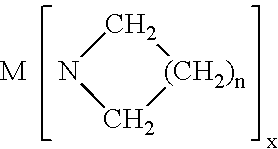
- the present invention relates to a CVD precursor composition for forming a thin film dielectric on a substrate, such precursor composition including at least one source reagent compound selected from the group consisting of:
- M is selected from the group consisting of: Zr, Hf, Y, La, Lanthanide series elements, Ta, Ti, Al; N is nitrogen; each of R 1 and R 2 is same or different and is independently selected from the group consisting of H, aryl, perfluoroaryl, C 1 -C 8 alkyl, C 1 -C 8 perfluoroalkyl, alkylsilyl; and x is the oxidation state on metal M; and n is from 1-6.
- lanthanides series elements refers to the 14 elements following lanthanum in the Periodic Table, viz., cerium, praseodymium, neodymium, promethium, samarium, europium, gadolinium, terbium, dysprosium, holmium, erbium, thulium, ytterbium and lutetium.
- the present invention relates to a CVD precursor composition for forming a thin film dielectric on a substrate, such precursor composition including at least one source reagent compound selected from the group consisting of:
- H is hydrogen; x is from 0 to 3; Si is silicon; A is a halogen; Y is from 0 to 3; N is nitrogen; each of R 1 and R 2 is same or different and is independently selected from the group consisting of H, aryl, perfluoroaryl, C 1 -C 8 alkyl, and C 1 -C 8 perfluoroalkyl; and n is from 1-6.
- the present invention relates to a CVD precursor composition for forming a thin film dielectric on a substrate, such precursor composition including a vapor source reagent selected from the group consisting of:
- M is selected from the group consisting of: Zr, Hf, Y, La, Lanthanide series elements, Ta, Ti, Al; N is nitrogen; each of R 1 and R 2 is same or different and is independently selected from the group consisting of H, aryl, perfluoroaryl, C 1 -C 8 alkyl, C 1 -C 8 perfluoroalkyl, alkylsilyl; and x is the oxidation state on metal M; and n is from 1-6.
- the present invention relates to a CVD precursor composition for forming a thin film dielectric on a substrate, such precursor composition including a vapor source reagent mixture including a metalloamide source reagent compound selected from the group consisting of:
- M is selected from the group consisting of: Zr, Hf, Y, La, Lanthanide series elements, Ta, Ti, Al; N is nitrogen; each of R 1 and R 2 is same or different and is independently selected from the group consisting of H, aryl, perfluoroaryl, C 1 -C 8 alkyl, C 1 -C 8 perfluoroalkyl, alkylsilyl; and x is the oxidation state on metal M; and n is from 1-6; and
- the present invention relates to a CVD single source precursor composition for forming a silicate thin film dielectric on a substrate, the precursor composition comprising a vapor source mixture comprising at least one metalloamide vapor source reagent selected from the group consisting of: M(NR 1 R 2 ) x ; and wherein M is selected from the group consisting of: Zr, Hf, Y, La, Lanthanide series elements, Ta, Ti, Al; N is nitrogen; each of R 1 and R 2 is same or different and is independently selected from the group consisting of H, aryl, perfluoroaryl, C 1 -C 8 alkyl, C 1 -C 8 perfluoroalkyl, alkylsilyl; and x is the oxidation state on metal M; and n is from 1-6; and H x SiA y (NR 1 R 2 ) 4-x-y ; and wherein H is hydrogen; x is from 0 to 3; Si is silicon; A is a hal
- Another aspect of the present invention relates to a CVD precursor composition
- a CVD precursor composition comprising a metalloamide source reagent compound and/or an aminosilane source reagent compound as described hereinabove, and a solvent medium in which the source reagent compound(s) is soluble or suspendable.
- the invention in another aspect, relates to formation of a dielectric thin film on a substrate from a precursor composition comprising a metalloamide source reagent compound, comprising vaporizing the precursor composition to form a vaporized precursor, and contacting the vaporized precursor with the substrate to deposit a metal-containing film thereon.
- the present invention relates to a CVD method of forming a dielectric thin film on a substrate, comprising the steps of:
- the present invention relates to a CVD method of forming a dielectric thin film on a substrate, comprising the steps of:
- the present invention relates to a method of making a gate dielectric and a gate electrode comprising the steps of:
- the present invention relates to a dielectric thin film formed by a method as described hereinabove.
- FIG. 1 is a cross-sectional view of a typical prior art integrated circuit field effect transistor.
- FIG. 2 A and FIG. 2B show a pressure temperature matrix for Hf(N(C 2 H 5 ) 2 ) 4 (Tetrakis(diethyl-amino)hafnium) and Hf(N(CH 3 ) 2 ) 4 (Tetrakis(dimethyl-amino)hafnium) in N 2 O.
- FIG. 3 shows the growth rate of hafnia films in different oxidizing ambients at 8 Torr and 550° C.
- FIGS. 4A and 4B show growth rate over process space for Hf(N(C 2 H 5 ) 2 ) 4 (Tetrakis(diethyl-amino)hafnium) and Hf(N(CH 3 ) 2 ) 4 (Tetrakis(dimethyl-amino)hafnium.
- FIG. 5 shows RMS roughness as measured by AFM over 1 ⁇ 1 ⁇ m areas of Hf(N(C 2 H 5 ) 2 ) 4 (Tetrakis(diethyl-amino)hafnium) and Hf(N(CH 3 ) 2 ) 4 (Tetrakis(dimethyl-amino)hafnium) thin films.
- FIG. 6 shows index of refraction measurements as a function of process conditions for Hf(N(CH 3 ) 2 ) 4 (Tetrakis(dimethyl-amino)hafnium) thin films.
- FIGS. 7A and 7B show a limited pressure-temperature matrix for Si(N(C 2 H 5 ) 2 ) 2 Cl 2 (Bis(diethyl-amino)dichlorosilane) and Si(N(CH 3 ) 2 ) 3 Cl (Tris(dimethyl-amino)chlorosilane in N 2 O.
- FIG. 8 shows the growth rate of silica from Si(N(C 2 H 5 ) 2 ) 2 Cl 2 (Bis(diethyl-amino)dichlorosilane) in N 2 O ambient.
- FIG. 9 shows the growth rate of silica from Si(N(CH 3 ) 2 ) 3 Cl (Tris(dimethyl-amino)chlorosilane in N 2 O ambient.
- FIG. 10 shows the growth rate of SiO 2 under a HfO 2 film with no silicon precursor present.
- FIG. 11 shows the growth rate of SiO 2 from Si(N(C 2 H 5 ) 2 ) 2 Cl 2 (Bis(diethyl-amino)dichlorosilane when co-deposited with HfO 2 from Hf(N(C 2 H 5 ) 2 ) 4 (Tetrakis(diethyl-amino)hafnium in N 2 O ambient.
- the metalloamide precursors of the present invention when utilized in a CVD process to deposit dielectric thin films on a substrate, result in a dielectric thin film having very low levels of carbon and little or no halide impurity. Further, when the metalloamide precursors of the present invention are used to deposit metal silicate gate dielectric thin films, the thickness of the SiO 2 interlayer is minimal or absent and the dielectric constant of the thin film is substantially higher than that of conventional thermal silicon.
- the gate dielectric thin films of the invention have low leakage currents, show relatively little growth of interfacial SiO 2 , and thus have high specific capacitance with low interface state density.
- the dielectric properties of the thin films produced by the method disclosed herein are substantially improved over conventional silicon gate structures.
- high temperature refers to a temperature in excess of 800° C.
- the invention in one embodiment relates to a CVD precursor composition for forming a thin film dielectric on a substrate, such precursor composition including a metalloamide source reagent compound selected from the group consisting of:
- M is selected from the group consisting of: Zr, Hf, Y, La, Lanthanide series elements, Ta, Ti, Al; N is nitrogen; each of R 1 and R 2 is same or different and is independently selected from the group consisting of H, aryl, perfluoroaryl, C 1 -C 8 alkyl, C 1 -C 8 perfluoroalkyl, alkylsilyl; and x is the oxidation state on metal M; and n is from 1-6.
- M is Zr or Hf
- R 1 and R 2 are methyl and/or ethyl
- the metalloamide source reagents useful for depositing dielectric thin films on a substrate include but are not limited to, compounds of the formula M(NMe 2 ) x , M(NEt 2 ) x , M(NMeEt) x .
- the metalloamide source reagent compound useful in the present invention may comprise an oligomer, i.e. Al 2 ( ⁇ -NMe 2 ) 2 (NMe 2 ) 4 .
- the metalloamide source reagents of the present invention are useful for forming dielectric thin films including but not limited to: gate dielectrics, high dielectric constant metal oxides, and ferroelectric metal oxides.
- the metalloamide source reagents are useful for forming gate dielectric thin films on a substrate, wherein the gate dielectric thin film may comprise a metal-oxide, a metal oxy-nitride, a metal silicate or a metal silicon-oxy-nitride. More preferably, the metalloamide source reagent is useful for forming a metal silicate gate dielectric thin film.
- the present invention relates to a CVD precursor composition for forming a thin film dielectric on a substrate, such precursor composition including at least one aminosilane source reagent compound selected from the group consisting of:
- H is hydrogen; x is from 0 to 3; Si is silicon; A is a halogen; Y is from 0 to 3; N is nitrogen; each of R 1 and R 2 is same or different and is independently selected from the group consisting of H, aryl, perfluoroaryl, C 1 -C 8 alkyl, and C 1 -C 8 perfluoroalkyl; and n is from 1-6.
- R 1 and R 2 are methyl and/or ethyl.
- the aminosilane source reagent compounds useful for depositing a dielectric thin film on a substrate include but are not limited to: Si(NMe 2 ) 3 Cl, Si(NEt 2 ) 2 Cl 2 , Si(NMe 2 ) 4 , and Si(NEt 2 ) 4 .
- the aminosilane source reagent compound may be used to deposit silicate or silicon oxy-nitride gate dielectric thin films on a substrate or the aminosilane source reagent may be used in combination with the metalloamide source reagent composition, as described hereinabove, to deposit a metal silicate or metal silicon-oxy-nitride gate dielectric thin film on a substrate.
- the invention in a further embodiment relates to a CVD precursor composition for forming a thin film dielectric on a substrate, such precursor composition including a metalloamide vapor source reagent compound selected from the group consisting of:
- M is selected from the group consisting of: Zr, Hf, Y, La, Lanthanide series elements, Ta, Ti, Al; N is nitrogen; each of R 1 and R 2 is same or different and is independently selected from the group consisting of H, aryl, perfluoroaryl, C 1 -C 8 alkyl, C 1 -C 8 perfluoroalkyl, alkylsilyl; x is the oxidation state on metal M; and n is from 1-6.
- the present invention relates to a CVD precursor composition for forming a thin film dielectric on a substrate, such precursor composition including at least one aminosilane vapor source reagent compound selected from the group consisting of:
- H is hydrogen; x is from 0 to 3; Si is silicon; A is a halogen; Y is from 0 to 3; N is nitrogen; each of R 1 and R 2 is same or different and is independently selected from the group consisting of H, aryl, perfluoroaryl, C 1 -C 8 alkyl, and C 1 -C 8 perfluoroalkyl; and n is from 1-6.
- R 1 and R 2 are methyl and/or ethyl.
- the aminosilane vapor source reagent compounds usefully employed in the present invention include, without limitation, Si(NMe 2 ) 3 Cl, Si(NEt 2 ) 2 Cl 2 , Si(NMe 2 ) 4 , and Si(NEt 2 ) 4 .
- the metalloamide CVD precursor composition is used to deposit a silicate gate dielectric thin film wherein the metalloamide precursor is suitably used in combination with a silicon precursor(s) source to yield the product metal silicate film.
- the silicon precursor may advantageously comprise an aminosilane source reagent compound as described herein or may alternatively comprise an alternative silicon source reagent compound as known to those skilled in the art, to deposit silicate thin films, (e.g. silane, trimethylsilane, tetramethylsilane and tetraethylorthosilicate).
- the metalloamide CVD precursor composition is bi-functional in that it may be used to deposit a gate dielectric thin film and a gate conductor, wherein the gate dielectric thin film is first deposited on a substrate using CVD conditions as described herein followed by deposition of a gate conductor on the gate dielectric substrate.
- the bi-functional nature of the metalloamide source reagent compound is advantageous in that it limits the number of process steps necessary to produce two components of a device structure.
- a (Hf, Si)O 4 gate dielectric thin film is CVD deposited on a substrate from Hf(NMe 2 ) 4 , Si(NMe 2 ) 4 and N 2 O process gas.
- a HfN gate conductor is deposited on the (Hf, Si)O 4 gate dielectric thin film of step one, from Hf(NMe 2 ) 4 and NH 3 process gas. This is especially useful for NMOS, where the fermi level of the gate conductor should be well matched to that in the channel.
- a precursor composition including at least one metalloamide source reagent compound and at least one aminosilane source reagent compound to produce a metal silicate dielectric thin film on a substrate, with the metalloamide source reagent compound containing at least part of the metal to be incorporated in the product dielectric metal silicate film, and the aminosilane source reagent compound containing at least part of the silicon to be incorporated in the product dielectric metal silicate film, it is possible by selection of the proportions of such respective compounds to correspondingly vary the stoichiometric composition (metal/silicon ratio) of the metal silicate dielectric film, to obtain a desired character of structural and performance properties in the product film.
- an aminosilane source reagent compound, containing no metal may be used in combination with a metalloamide source reagent compound, containing no silicon, to control film ratios, (i.e., Zr/Si or Hf/Si).
- the present invention relates to a CVD precursor composition for forming a silicate thin film dielectric on a substrate, such precursor including a vapor source mixture comprising at least one metalloamide vapor source reagent compound as described hereinabove and at least one aminosilane vapor source reagent compound as described hereinabove, wherein the relative proportions of the aminosilane vapor source reagent and the metalloamide vapor source reagent relative to one another are employed to controllably establish the desired M x /Si 1-x ratio in the deposited silicate thin films, wherein M x /Si 1-x is from about 0.01 to 10.
- the exact composition will be a trade off between high Si films, which prevent crystallization during subsequent high temperature processing, and high M films, which have higher dielectric constant (lower EOT).
- the present invention relates to a CVD precursor solution composition for forming a thin film dielectric on a substrate, such precursor composition including at least one metalloamide compound as described hereinabove and a solvent medium in which the metalloamide compound is soluble or suspendable, wherein the metalloamide compound and the solvent medium are combined to produce a precursor solution mixture for depositing a dielectric thin film on a substrate.
- the present invention relates to a CVD precursor solution composition for forming a thin film dielectric on a substrate, such source reagent composition including at least one aminosilane compound as described hereinabove and a solvent medium in which at least one aminosilane compound is soluble or suspendable, wherein the aminosilane precursor compound and the solvent medium are combined to produce a precursor solution mixture for depositing a silicon containing dielectric thin film on a substrate.
- the present invention relates to a CVD multi-component, single source precursor composition useful for forming a thin film dielectric on a substrate, such source composition including at least one metalloamide compound as described hereinabove, at least one aminosilane compound as described hereinabove and a solvent medium in which the metalloamide compound and the aminosilane compound are soluble or suspendable, wherein the metalloamide source reagent compound, the aminosilane compound, and the solvent medium are combined to produce a chemically compatible, single source solution mixture for depositing a silicon containing dielectric thin film on a substrate.
- Providing a precursor composition in liquid (i.e., neat solution or suspension) form facilitates rapid volatilization (i.e., flash vaporization) of the source reagent composition and transport of the resultant precursor vapor to a deposition locus such as a CVD reaction chamber.
- the metalloamide and aminosilane compounds of the present invention are chosen to provide a degenerate sweep of ligands, to eliminate ligand exchange and to provide a robust precursor delivery, gas-phase transport and CVD process.
- the precursor compositions of the present invention may comprise any suitable solvent medium that is compatible with the metalloamide and/or aminosilane compounds contained therein.
- the solvent medium in such respect may comprise a single component solvent, or alternatively a solvent mixture or solution.
- Illustrative solvent media that may be variously usefully employed include ethers, glymes, tetraglymes, amines, polyamines, aliphatic hydrocarbon solvents, aromatic hydrocarbon solvents, cyclic ethers, and compatible combinations of two or more of the foregoing.
- a particularly preferred solvent species useful in the practice of the present invention is octane.
- the source reagent compounds of the invention are stable, even in organic solutions, while at the same time they are volatilizable at low temperatures that are consistent with efficient chemical vapor deposition processing.
- the source reagent compounds of the present invention also possess the following advantageous features: good deposition rates; good thermal stability; higher elemental purity; formation of essentially carbon-free films (in contrast to the reported literature, i.e. Jones, et al., “MOCVD of Zirconia Thin Films by Direct Liquid Injection Using a New Class of Zirconium Precursor”, Chem. Vap. Dep ., Vol. 4, 1998, PP. 46-49.); limited SiO 2 interlayer formation; ready decomposition at CVD process temperatures; and good solubility in a wide variety of organic solvents and solvent media.
- composition or method may contain or involve additional, (i.e., third and fourth) metalloamide and/or aminosilane compounds.
- the metalloamide and aminosilane source reagent compounds of the invention and methods of making are well known in the art and may be obtained from commercial sources or readily prepared by published synthetic routes. See, D. C. Bradley and I. M. Thomas, “Metalorganic Compounds Containing Metal-Nitrogen Bonds: Part I. Some Dialkylamino Derivatives of Titanium and Zirconium”, J. Chem. Soc., 1960, 3857) (D. C. Bradley and I. M. Thomas, “Metalorganic Compounds Containing Metal-Nitrogen Bonds: Part III. Dialkylamino Compounds of Tantalum”, Canadian J. Chem., 40, 1355 (1962). Many of the metalloamide and aminosilane source reagent compounds of the present invention are available commercially through ATMI, Inc., Inorgtech, Gelest, Inc., Aldrich Chemical Company and Strem Chemical Company.
- the present invention relates to a method for forming a dielectric thin film on a substrate by chemical vapor deposition.
- Such method includes the steps of:
- M is selected from the group consisting of: Zr, Hf, Y, La, Lanthanide series elements, Ta, Ti, Al; N is nitrogen; each of R 1 and R 2 is same or different and is independently selected from the group consisting of H, aryl, perfluoroaryl, C 1 -C 8 alkyl, C 1 -C 8 perfluoroalkyl, alkylsilyl; and x is the oxidation state on metal M; and n is from 1-6;
- the present invention relates to a method for forming a dielectric silicate thin film on a substrate by chemical vapor deposition.
- Such method includes the steps of:
- the metalloamide and aminosilane compounds of the present invention may be used independently or in combination to form the desired dielectric thin film.
- the metalloamide and aminosilane compound may be vaporized and deposited simultaneously or sequentially to obtain a dielectric thin film having the desired property.
- CVD chemical vapor deposition
- ACVD atomic layer chemical vapor deposition
- a metalloamide precursor vapor is introduced into a chemical vapor deposition chamber comprising a substrate, in a sequential or “pulsed” deposition mode, during which time, extremely co-reactive gases may be employed, such as ozone, water vapor or reactive alcohols, that might normally be expected to produce deleterious deposition effects on the CVD process (i.e., gas phase particle formation).
- extremely co-reactive gases such as ozone, water vapor or reactive alcohols, that might normally be expected to produce deleterious deposition effects on the CVD process (i.e., gas phase particle formation).
- the atomic layer chemical vapor deposition method of the present invention may further comprise an aminosilane precursor vapor that may be simultaneously co-pulsed and co-deposited with the metalloamide precursor vapor, on a substrate.
- the aminosilane precursor vapor may be deposited on a substrate in a sequential pulsing method, wherein the aminosilane compound alternates pulses with the metalloamide compound.
- the dielectric thin films are built up by introducing short bursts of gases in cycles.
- a co-reactant may be used in a pulsed or atomic layer chemical vapor deposition method, wherein the metalloamide precursor and/or aminosilane precursor vapor is separated from the co-reactant by time in the pulse track.
- the co-reactant may be utilized to facilitate the decomposition of the precursor on a substrate, within a desired temperature regime and to produce carbon-free dielectric thin-films.
- the use of water vapor may be utilized to induce a lower decomposition temperature of the aminosilane precursor vapor, which in some instances has been found to be stable in oxidizing environments such as N 2 O.
- pulse track and number of cycles may be varied. In a typical ALCVD process, a cycle lasts from 1-5 seconds.
- the following non-limiting examples demonstrate various pulse tracks defining precursor(s) and co-reactant(s) that may be successfully used to deposit the dielectric thin films of the present invention:
- the source liquid may comprise the source reagent compound(s) if the compound or complex is in the liquid phase at ambient temperature (e.g., room temperature, 25° C.) or other supply temperature from which the source reagent is rapidly heated and vaporized to form precursor vapor for the CVD process.
- ambient temperature e.g., room temperature, 25° C.
- the source reagent compound or complex is a solid at ambient or the supply temperature, such compound or complex can be dissolved or suspended in a compatible solvent medium therefore to provide a liquid phase composition that can be submitted to the rapid heating and vaporization to form precursor vapor for the CVD process.
- the precursor vapor resulting from the vaporization then is transported, optionally in combination with a carrier gas (e.g., He, Ar, H 2 , O 2 , etc.), to the chemical vapor deposition reactor where the vapor is contacted with a substrate at elevated temperature to deposit material from the vapor phase onto the substrate or semiconductor device precursor structure positioned in the CVD reactor.
- a carrier gas e.g., He, Ar, H 2 , O 2 , etc.
- the precursor liquid may be vaporized in any suitable manner and with any suitable vaporization means to form corresponding precursor vapor for contacting with the elevated temperature substrate on which the dielectric film is to be formed.
- the vaporization may for example be carried out with a liquid delivery vaporizer unit of a type as commercially available from Advanced Technology Materials, Inc. (Danbury, Conn.) under the trademark SPARTA and VAPORSOURCE II, in which precursor liquid is discharged onto a heated vaporization element, such as a porous sintered metal surface, and flash vaporized.
- the vaporizer may be arranged to receive a carrier gas such as argon, helium, etc. and an oxygen-containing gas may be introduced as necessary to form the dielectric thin film.
- the precursor vapor thus is flowed to the chemical vapor deposition chamber and contacted with the substrate on which the dielectric film is to be deposited.
- the substrate is maintained at a suitable elevated temperature during the deposition operation by heating means such as a radiant heating assembly, a susceptor containing a resistance heating element, microwave heat generator, etc.
- heating means such as a radiant heating assembly, a susceptor containing a resistance heating element, microwave heat generator, etc.
- Appropriate process conditions of temperature, pressure, flow rates and concentration (partial pressures) of metal and silicon components are maintained for sufficient time to form the dielectric film at the desired film thickness, (i.e., in a range of from about 2 nanometers to about 1000 micrometers), and with appropriate dielectric film characteristics.
- the step of vaporizing the source reagent compounds of the present invention is preferably carried out at a vaporization temperature in the range of from about 50° C. to about 300° C. Within this narrow range of vaporization temperature, the metalloamide and aminosilane source reagent compounds are effectively vaporized with a minimum extent of premature decomposition.
- suitable carrier gas species include gases that do not adversely affect the dielectric film being formed on the substrate.
- gases include argon, helium, krypton or other inert gas, with argon gas generally being most preferred.
- argon gas may be introduced for mixing with the vaporized source reagent composition at a flow rate of about 100 standard cubic centimeters per minute (sccm).
- Oxidizing gases useful for the broad practice of the present invention include, but are not limited to, O 2 , N 2 O, NO, H 2 O and 03, More preferably, the oxidizer used comprises N 2 O.
- the deposition of the dielectric thin films of the present invention are preferably carried out under an elevated deposition temperature in a range of from about 250° C. to about 750° C.
- Hf(NMe 2 ) 4 and Si(Me) 4 may be mixed in a gas stream, (i.e., in a carrier gas), and mixed in the gas stream to the CVD reactor to produce the appropriate stoichiometry in a deposited HfSiO 4 thin-film.
- Other metalloamides of the invention and silanes may be similarly employed with equivalent success, provided that the respective ligands do not produce undesirable non-degenerate ligand exchanges forming (undesired) new precursor species. It therefore is preferred to use the same ligand species, (ie., methyl, ethyl, phenyl, etc.) for each of the metalloamide and silicon precursors used in combination with one another.
- Hf(NMe 2 ) 4 and Si(NMe 2 ) 4 may be mixed in a gas stream, (ie., in a carrier gas), and mixed in the gas stream to the CVD reactor to produce the appropriate stoichiometry in a deposited Hf x Si 2-x O 4 thin-film, wherein x is from 0 to 1.
- Other metalloamides of the invention and aminosilanes may be similarly employed with equivalent success, provided that the respective ligands do not produce undesirable non-degenerate ligand exchanges forming (undesired) new precursor species. It therefore is preferred to use the same ligand species, (i.e., methyl, ethyl, phenyl, etc.) for each of the metalloamide and aminosilane precursors used in combination with one another.
- a representative liquid delivery chemical vapor deposition approach is illustrated by the use of metalloamide source reagent compound, Zr(NMe 2 ) 4 and aminosilane source reagent compound Si(NMe 2 ) 4 .
- the source reagent compounds are introduced into a chemical vapor deposition chamber using liquid delivery and oxidized in-situ to deposit on a substrate, the desired Zr silicate thin film composition based upon electrical performance and film stoichiometry.
- La(NMe 2 ) 3 may be added to the mixture to produce a Zr La doped silicate dielectric film under similar processing conditions.
- a representative liquid delivery chemical vapor deposition approach is illustrated by the use of metalloamide source reagent compound, Y(NMe 2 ) 3 and aminosilane source reagent compound Si(NEt 2 ) 4
- the source reagent compounds are introduced into a chemical vapor deposition chamber using liquid delivery and oxidized in-situ to deposit on a substrate, the desired Y silicate thin film composition based upon electrical performance and film stoichiometry.
- a representative liquid delivery chemical vapor deposition approach is illustrated by the use of metalloamide source reagent compounds Hf(NMe 2 ) 4 and La(NMe 2 ) 3 and aminosilane source reagent compound Si(NEt 2 ) 4 .
- the source reagent compounds are introduced into a chemical vapor deposition chamber using liquid delivery and oxidized in-situ to deposit on a substrate, the desired HfLa silicate thin film composition based upon electrical performance and film stoichiometry.
- Zr(NMe 2 ) 4 may be added to the mixture to produce Zr doped silicate films under similar processing conditions.
- the present invention relates to a dielectric thin film, having a dielectric constant value in a range between about 4 to about 60 as measured at a frequency of 1 mega-Hertz, produced by a method comprising the steps of:
- the present invention relates to a silicon containing dielectric thin film, having a dielectric constant in a range between about 4 to about 60 as measured at a frequency of 1 mega-Hertz, by a method comprising the steps:
- the dielectric metal silicate thin films produced from the metalloamide materials of the present invention are pure metal silicate thin films comprising little or no carbon or halogen impurity.
- the dielectric silicate thin films contain less than 1 atomic percent carbon and more preferably the thin films contain less than 1 ppm carbon and no detectable halogen.
- the dielectric silicate films produced in the broad practice of the invention include stoichiometric metal silicate films, as well as off-stoichiometric (metal-deficient) films.
- the precursor composition includes different source reagents providing respectively differential metal and/or silicon content
- the respective source reagents can be supplied in varied compositions to achieve desired stoichiometric characteristics in the corresponding product metal silicate films. In this manner, the electrical properties, including dielectric constant and leakage, can be controlled and closely tailored to a desired end use.
- the dielectric thin films produced by a method of the present invention are useful as, but not limited to: gate dielectric thin films, more particularly metal silicate gate dielectric thin films and metal oxy-nitride gate dielectric thin films; metal oxide high dielectric thin films; and ferroelectric thin films.
- the presence of nitrogen, in at least a partial thickness of the gate dielectric helps to prevent the diffusion of boron, such as from a boron-doped polysilcon gate electrode, to the channel region.
- Exemplary dielectric thin films formed by the method of the present invention include but are not limited to: ZrSiO 4 ; HfSiO 4 ; Ta 1-x Al x O y , where x is 0.03-0.7 and y is 1.5-205; Ta 1-x Si x O y , where x is 0.05-0.15 and y is 1.5-3; Ta 1-x-z Al x Si z O y , where 0.7>x+z>0.05, z ⁇ 0.15 and y is 1.5-3; HfO 2 ; ZrO 2 ; Ta 2 O 5 ; Zr x Si 2-x O 4 where x is 0.2-1.6; Hf x Si 2-x O 4 , where x is 0.2-1.6; Hf x La y Si 2-x O 4+1.5y , where x is 0.2-1.6 and y is 0-1; Zr x La y Si 2-x O 4+1.5y , where x is 0.2-1.6 and y is 0-1; Hf
- HfO 2 is a component of many of the proposed alternative high k gate dielectrics.
- One of the issues in growing a gate dielectric by a CVD process is minimizing the growth of interfacial SiO 2 .
- interfacial SiO 2 will grow even if the only oxygen present in the process is in an oxygen-containing precursor, such as an alkoxide or a mixed alkoxide- ⁇ -diketonate.
- an oxygen-containing precursor such as an alkoxide or a mixed alkoxide- ⁇ -diketonate.
- TDMAHf and TDEAHf has been studied.
- Carbon-free HfO 2 can be grown at high deposition rates from these precursors at temperatures down to 400° C. in an ambient of N 2 O. It is quite unexpected that N 2 O is effective at oxidizing the precursor at such low temperatures and there is no sign of the process getting worse at lower temperatures either with increase carbon or lower deposition rate.
- Ta 2 O 5 and doped Ta 2 O 5 might also grow as clean amorphous films at low temperatures from alkylamido precursors in N 2 O.
- Hafnia films were grown with the precursors listed in Table I. Precursor solutions were prepared at 0.1M Hf in octane. Substrate of (100) Si was prepared with an SC1 treatment followed by dilute HF to remove any SiO 2 on the surface. The generic process conditions for the experiments are shown in Table II. Initially, films were grown at 550° C. under three different reactive gas conditions: Ar, N 2 O and O 2 . Results described below indicated that N 2 O was the preferred ambient. A pressure-temperature matrix was performed for each precursor using the N 2 O ambient as shown in FIGS. 2A and 2B . FIGS. 2A and 2B show the process space experiments for TDEAHf and TDMAHf precursors. At the end, a film targeting 50 ⁇ was grown from each precursor to be used for TEM examination of the interface with Si.
- Film thickness was measured using single-wavelength ellipsometry at 70° incidence angle, and XRF.
- HfO 2 the XRF was calibrated by assuming the X-ray efficiencies were equivalent to TaO 2.5 , for which we have standards that have been measured by RBS.
- the growth rate of hafnia was measured by XRF for films grown in different oxidizing ambients at 8 Torr and 550° C. as shown in FIG. 3 .
- the compositions of these films were measured by XPS.
- the films grown in the inert Ar environment had a high growth rate, but this growth was accompanied by considerable carbon and some nitrogen incorporation.
- Films grown in N 2 O were surprisingly carbon-free, but with a low growth rate. No film growth was detected for the run performed in O 2 . With these results, further examination of pressure and temperature were performed in a N 2 O ambient.
- the growth rate as measured by XRF varied over process space for the two precursors as shown in FIGS. 4A and 4B .
- the growth rate is low at higher temperatures and pressures.
- the growth rate is largely independent of temperature, and at 400° C. the growth rate is largely independent of pressure.
- the growth rate of TDEAHf is slightly lower than TDMAHf, but both have rates that are sufficient for manufacturable deposition.
- the RMS roughness of the films was measured by AFM over a 1 ⁇ 1 ⁇ m areas and the results plotted as a function of film thickness as shown in FIG. 5 .
- Films generally roughen somewhat as they become thicker, so that it is important to compare their morphology to others of the same thickness.
- films grown at 400° C. are smoother than those grown at higher temperatures.
- the growth time was shorter for the TDMAHf films, so they were much thinner and also smoother.
- a film was grown for each precursor to a thickness of about 50 ⁇ . In both cases, the RMS roughness was about 6 ⁇ .
- Film thickness and index of refraction were measured by ellipsometry for all films. Those grown from TDEAHf were thick and the resulting roughness prevented reliable ellipsometry measurements.
- the index of refraction of the films grown from TDMAHf is shown as a function of process condition in FIG. 6 .
- the films grown at lower temperature exhibited higher refractive index, which probably indicates either a more dense film or a film with less SiO 2 incorporated from the substrate.
- TEM was used to examine the interface of a nominal 50 ⁇ film grown from each of the precursors at 400° C.
- Film G161 was grown at 400° C., 8 Torr from TDMAHf with a growth time of 43 seconds;
- Film G163 was grown at 400° C., 0.8 Torr from TDEAHf with a growth time of 60 seconds.
- TEM showed the interfaces of both films with underlying Si to be clean of any interfacial silicon oxide.
- the films are crystalline. It is expected that mixing Si oxide with the Hf oxide in the growth process would yield an amorphous film.
- interfacial SiO 2 One of the issues in growing a gate dielectric by a CVD process is minimizing the growth of interfacial SiO 2 .
- interfacial SiO 2 will grow even if the only oxygen present in the process is in an oxygen-containing precursor, such as an alcoxide or a mixed alcoxide- ⁇ -diketonate.
- the experiment discussed hereinabove demonstrated the viability of two hafnia precursors specifically, Hf(NMe 2 ) 4 and Hf(Net 2 ) 4 hereafter referred to as TDMAHf and TDEAHf, respectively.
- This experiment examines the viability of the corresponding silicon precursors: Si(NMe 2 ) 3 Cl and Si(NEt 2 ) 2 Cl 2 .
- the silica precursors are examined using the same process conditions.
- Silica films were grown with the silicon precursors listed in Table III, Si(NMe 2 ) 3 Cl and Si(NEt 2 ) 2 Cl 2 . Precursor solutions were prepared at 0.1M Si in octane. Substrates of (100) Si were prepared with an SC1 treatment followed by dilute HF to remove any native SiO 2 . The generic process conditions for the experiments are shown in Table IV. Results from the growth of hafnia films encouraged us to center these initial experiments on growth in an N 2 O atmosphere although growth in O 2 or other oxidizer could be used at temperatures at or below 500° C. A limited pressure-temperature matrix was performed for each Si precursor using the N 2 O ambient as shown in FIGS. 7A and 7B .
- Si(NEt 2 ) 2 Cl 2 is compatible with TDEAHf in solution, with any ligand exchange being degenerate.
- Si(NMe 2 ) 3 Cl is compatible with both TDEAHf and TDMAHf.
- a solution of 0.05M TDEAHf:0.05M Si(NEt 2 ) 2 Cl 2 was produced by mixing the two 0.1M solutions. This mixture was used to grow films over the entire matrix of process conditions.
- Film thickness was measured using single-wavelength ellipsometry at 70° incidence angle, and XRF.
- n 1.46, typical of high quality thermal oxide.
- the XRF was calibrated by assuming the X-ray efficiencies were equivalent to TaO 2.5 , for which standards that been measured by RBS.
- the Hf:Si composition was estimated by assuming that both are fully oxidized and fully dense.
- the ellipsometric thickness not accounted for by HfO 2 was assigned to SiO 2 , and composition was calculated from these two thicknesses.
- the films have a mixed Si:Hf composition on the film surface.
- the constant SiO 2 growth rate over the range of 500-600° C. at 2.2 Torr being the same as 0.8 Torr at 600° C. is taken as evidence of mass transport limited deposition over the range of the process.
- the addition of water vapor or O 2 should further decrease the temperature window wherein both Hf and Si alkylamido precursors transport and decompose reliably.
Landscapes
- Chemical & Material Sciences (AREA)
- Organic Chemistry (AREA)
- Chemical Kinetics & Catalysis (AREA)
- Engineering & Computer Science (AREA)
- Materials Engineering (AREA)
- Mechanical Engineering (AREA)
- Metallurgy (AREA)
- Inorganic Chemistry (AREA)
- General Chemical & Material Sciences (AREA)
- Chemical Vapour Deposition (AREA)
- Formation Of Insulating Films (AREA)
- Insulated Gate Type Field-Effect Transistor (AREA)
Abstract

wherein M is Zr, Hf, Y, La, Lanthanide series elements, Ta, Ti, or Al; N is nitrogen; each of R1 and R2 is same or different and is independently selected from H, aryl, perfluoroaryl, C1-C8 alkyl, C1-C8 perfluoroalkyl, alkylsilyl; and x is the oxidation state on metal M; and an aminosilane compound of the formula HxSiAy(NR1R2)4-x-y or

wherein H is hydrogen; x is from 0 to 3; Si is silicon; A is a halogen; Y is from 0 to 3; N is nitrogen; each of R1 and R2 is same or different and is independently selected from the group consisting of H, aryl, perfluoroaryl, C1-C8 alkyl, and C1-C8 perfluoroalkyl; and n is from 1-6. By comparison with the standard SiO2 gate dielectric materials, these gate dielectric materials provide low levels of carbon and halide impurity.
Description
M(NR1R2)x; and

HxSiAy(NR1R2)4-x-y and

M(NR1R2)x; and

M(NR1R2)x; and

- an aminosilane source reagent compound selected from the group consisting of:
HxSiAy(NR1R2)4-x-y;
and
wherein H is hydrogen; x is from 0 to 3; Si is silicon; A is a halogen; Y is from 0 to 3; N is nitrogen; each of R1 and R2 is same or different and is independently selected from the group consisting of H, aryl, perfluoroaryl, C1-C8 alkyl, and C1-C8 perfluoroalkyl; and n is from 1-6.
M(NR1R2)x;
and

wherein M is selected from the group consisting of: Zr, Hf, Y, La, Lanthanide series elements, Ta, Ti, Al; N is nitrogen; each of R1 and R2 is same or different and is independently selected from the group consisting of H, aryl, perfluoroaryl, C1-C8 alkyl, C1-C8 perfluoroalkyl, alkylsilyl; and x is the oxidation state on metal M; and n is from 1-6; and
HxSiAy(NR1R2)4-x-y;
and

wherein H is hydrogen; x is from 0 to 3; Si is silicon; A is a halogen; Y is from 0 to 3; N is nitrogen; each of R1 and R2 is same or different and is independently selected from the group consisting of H, aryl, perfluoroaryl, C1-C8 alkyl, and C1-C8 perfluoroalkyl; and n is from 1-6.
-
- vaporizing a precursor composition comprising at least one metalloamide source reagent compound to form a source reagent precursor vapor;
- transporting the source reagent precursor vapor into a chemical vapor deposition zone, optionally using a carrier gas;
- contacting the source reagent precursor vapor with a substrate in said chemical vapor deposition zone at elevated temperature to deposit a dielectric thin film on the substrate.
-
- vaporizing a multicomponent precursor composition mixture comprising at least one metalloamide source reagent compound and at least one aminosilane source reagent compound, to form a source reagent precursor vapor;
- transporting the source reagent precursor vapor into a chemical vapor deposition zone, optionally using a carrier gas;
- contacting the source reagent precursor vapor with a substrate in said chemical vapor deposition zone at elevated temperature, to deposit a dielectric thin film on the substrate.
-
- vaporizing a precursor composition comprising at least one metalloamide source reagent compound to form a source reagent precursor vapor;
- transporting the source reagent precursor vapor into a chemical vapor deposition zone, optionally using a carrier gas;
- contacting the source reagent precursor vapor with a substrate in said chemical vapor deposition zone at elevated temperature to deposit a dielectric thin film on the substrate;
- vaporizing a precursor composition comprising at least one metalloamide source reagent compound to form a source reagent precursor vapor;
- transporting the source reagent precursor vapor into a chemical vapor deposition zone, optionally using a carrier gas;
- contacting the source reagent precursor vapor with a substrate, comprising the dielectric thin film, in said chemical vapor deposition zone at elevated temperature to deposit a gate conducting thin film on the dielectric thin film.
-
- U.S. patent application Ser. No. 09/414,133 filed Oct. 7, 1999 in the names of Thomas H. Baum, et al.;
- U.S. patent application Ser. No. 09/012,679 filed Jan. 23, 1998 in the names of Gautam Bhandari, et al., and issued Jan. 18, 2000 as U.S. Pat. No. 6,015,917;
- U.S. patent application Ser. No. 08/979,465 filed Nov. 26, 1997 in the names of Frank DiMeo, Jr., et al., and issued Oct. 26, 1999 as U.S. Pat. No. 5,972,430;
- U.S. patent application Ser. No. 08/835,768 filed Apr. 8, 1997 in the names of Thomas H. Baum, et al., and issued Jul. 6, 1999 as U.S. Pat. No. 5,919,522;
- U.S. patent application Ser. No. 08/484,654 filed Jun. 7, 1995 in the names of Robin A. Gardiner et al., and issued Aug. 29, 2000 as U.S. Pat. No. 6,110,529;
- U.S. patent application Ser. No. 08/414,504 filed Mar. 31, 1995 in the names of Robin A. Gardiner et al., and issued Oct. 13, 1998 as U.S. Pat. No. 5,820,664;
- U.S. patent application Ser. No. 08/280,143 filed Jul. 25, 1994 in the names of Peter S. Kirlin, et al., and issued Jul. 16, 1996 as U.S. Pat. No. 5,536,323;
- U.S. patent application Ser. No. 07/927,134, filed Aug. 7, 1992 in the same names;
- U.S. patent application Ser. No. 07/807,807 filed Dec. 13, 1991 in the names of Peter S. Kirlin, et al., and issued Apr. 20, 1993 as U.S. Pat. No. 5,204,314;
- U.S. patent application Ser. No. 08/181,800 filed Jan. 15, 1994 in the names of Peter S. Kirlin, et al., and issued Sep. 26, 1995 as U.S. Pat. No. 5,453,494;
- U.S. patent application Ser. No. 07/918,141 filed Jul. 22, 1992 in the names of Peter S. Kirlin, et al., and issued Jan. 18, 1994 as U.S. Pat. No. 5,280,012;
- U.S. application Ser. No. 07/615,303 filed Nov. 19, 1990;
- U.S. patent application Ser. No. 07/581,631 filed Sep. 12, 1990 in the names of Peter S. Kirlin, et al., and issued Jul. 6, 1993 as U.S. Pat. No. 5,225,561.
- U.S. patent application Ser. No. 07/549,389 filed Jul. 6, 1990 in the names of Peter S. Kirlin, et al.
- U.S. patent application Ser. No. 08/758,599 filed Nov. 27, 1996 in the names of Jeffrey F. Roeder, et al., and issued Mar. 2, 1999 as U.S. Pat. No. 5,876,503.
M(NR1R2)x; and

HxSiAy(NR1R2)4-x-y; and

M(NR1R2)x; and

HxSiAy(NR1R2)4-x-y; and

-
- vaporizing a precursor composition comprising at least one metalloamide source reagent compound selected from the group consisting of:
M(NR1R2)x; and

-
- , as described hereinabove, to form a source reagent precursor vapor,
- transporting such source reagent precursor vapor into a chemical vapor deposition zone containing a substrate, optionally using a carrier gas to effect such transport;
- contacting the source reagent precursor vapor with a substrate in such chemical vapor deposition zone in the presence of an oxidizer and at elevated temperature to deposit a corresponding M containing dielectric thin film.
-
- vaporizing a precursor composition comprising at least one aminosilane compound selected from the group consisting of:
HxSiAy(NR1R2)4-x-y; and

-
- as described hereinabove, to form a source reagent precursor vapor;
- transporting such source reagent precursor vapor into a chemical vapor deposition zone containing a substrate, optionally using a carrier gas to effect such transport;
- contacting the source reagent precursor vapor with a substrate in such chemical vapor deposition zone in the presence of an oxidizer and at elevated temperature to deposit a corresponding Si containing dielectric thin film.
-
example track 1—(metalloamide/purge (inert)/co-reactant+N2O/purge (inert))n cycles; -
example track 2—(metalloamide+aminosilane/purge (inert)/N2O/purge (inert))n cycles; -
example track 3—(metalloamide+co-reactant N2O/co-reactant water vapor/purge (inert))n cycles; -
example track 4—(metalloamide+co-reactant N2O/aminosilane/co-reactant water vapor/purge (inert))n cycles. - wherein n is an integer number, typically ranging from 10 to 100, and different co-reactants have different oxidizing potentials.
-
- vaporizing a precursor composition comprising at least one metalloamide compound selected from the group consisting of:
M(NR1R2)x; and
-
- as described hereinabove, to form a source reagent precursor vapor;
- transporting such source reagent precursor vapor into a chemical vapor deposition zone containing a substrate, optionally using a carrier gas to effect such transport;
- contacting the source reagent precursor vapor with a substrate in such chemical vapor deposition zone in the presence of an oxidizer and at elevated temperature to deposit a corresponding M containing dielectric thin film.
-
- vaporizing a source reagent precursor composition comprising at least one aminosilane compound selected from the group consisting of:
HxSiAy(NR1R2)4-x-y; and

-
- as described hereinabove, to form a source reagent precursor vapor;
- transporting such source reagent precursor vapor into a chemical vapor deposition zone containing a substrate, optionally using a carrier gas to effect such transport;
- contacting the source reagent precursor vapor with a substrate in such chemical vapor deposition zone in the presence of an oxidizer and at elevated temperature to deposit a corresponding silicate dielectric thin film.
| TABLE I |
| Precursors used for film deposition. |
| Tetrakis(diethyl-amino)hafnium | Hf(N(C2H5))4 | TDEAHf |
| Tetrakis(dimethyl-amino)hafnium | Hf(N(CH3))4 | TDMAHf |
| TABLE II |
| Generic process conditions for zirconia and hafnia films |
| Precursor solution | 0.10 M in octane | ||
| Precursor solution delivery rate | 0.10 ml/min | ||
| Vaporization Temperature | 150° C. | ||
| Run time | 10-30 | ||
| Carrier gas | |||
| 100 sccm Ar | |||
| Heating and |
500 sccm Ar | ||
| Run |
400 sccm N2O or O2 | ||
| Pressure | 0.8, 2.2, or 8.0 Torr | ||
| Temperature | 400-600° C. wafer surface | ||
| TABLE III |
| Precursors used for film deposition. |
| (Bis(diethyl-amino)dichlorosilane) | Si(N(C2H5)2)2Cl2 | |
| (Tris(dimethyl-amino)chlorosilane) | Si(N(CH3)2)3Cl | |
| Tetrakis(diethyl-amino)hafnium | Hf(N(C2H5)2)4 | TDEAHf |
| Tetrakis(dimethyl-amino)hafnium | Hf(N(CH3)2)4 | TDMAHf |
| TABLE IV |
| Generic process conditions |
| Precursor solution | 0.10 M in octane | ||
| Precursor solution delivery rate | 0.10 ml/min | ||
| Vaporization Temperature | 150° | ||
| Run time | |||
| 10 | |||
| Carrier gas | |||
| 100 sccm Ar | |||
| Heating and |
500 sccm Ar | ||
| Run |
400 sccm N2O | ||
| Pressure | 0.8, 2.2, or 8.0 Torr | ||
| Temperature | 400-650° C. wafer surface | ||
Claims (46)
M(NR1R2)x; and

HxSiAy(NR1R2)4-x-y; and

HxSiAy(NR1R2)4-x-y; and

HxSiAy(NR1R2)4-r-yt
HxSiAy(NR1R2)4-x-y; and

M(NR1R2)x; and

M(NR1R2)x; and

HxSiAy(NR1R2)4-x-y; and

M(NR1R2)x; and

Priority Applications (10)
| Application Number | Priority Date | Filing Date | Title |
|---|---|---|---|
| US09/954,831 US6869638B2 (en) | 2001-03-30 | 2001-09-18 | Source reagent compositions for CVD formation of gate dielectric thin films using amide precursors and method of using same |
| EP02728580A EP1373278A4 (en) | 2001-03-30 | 2002-03-27 | METALLOAMIDE AND AMINOSILANE PRECURSORS USED IN CVD FORMATION OF DIELECTRIC THIN FILMS |
| JP2002577835A JP2004529495A (en) | 2001-03-30 | 2002-03-27 | Metal amide precursor and aminosilane precursor for CVD formation of dielectric thin film |
| PCT/US2002/009390 WO2002079211A1 (en) | 2001-03-30 | 2002-03-27 | Metalloamide and aminosilane precursors for cvd formation of dielectric thin films |
| KR1020087030848A KR20090009989A (en) | 2001-03-30 | 2002-03-27 | Metalloamide and Aminosilane Precursors for CDD Formation of Dielectric Thin Films |
| KR10-2003-7012687A KR20030094310A (en) | 2001-03-30 | 2002-03-27 | Metalloamide and aminosilane precursors for cvd formation of dielectric thin films |
| US10/112,517 US7084080B2 (en) | 2001-03-30 | 2002-03-29 | Silicon source reagent compositions, and method of making and using same for microelectronic device structure |
| US11/301,043 US20060099831A1 (en) | 2001-03-30 | 2005-12-12 | Silicon source reagent compositions, and method of making and using same for microelectronic device structure |
| US11/363,904 US20060148271A1 (en) | 2001-03-30 | 2006-02-28 | Silicon source reagent compositions, and method of making and using same for microelectronic device structure |
| JP2008158310A JP2008300850A (en) | 2001-03-30 | 2008-06-17 | Metal amide precursors and aminosilane precursors for CVD formation of dielectric thin films |
Applications Claiming Priority (2)
| Application Number | Priority Date | Filing Date | Title |
|---|---|---|---|
| US09/823,196 US7005392B2 (en) | 2001-03-30 | 2001-03-30 | Source reagent compositions for CVD formation of gate dielectric thin films using amide precursors and method of using same |
| US09/954,831 US6869638B2 (en) | 2001-03-30 | 2001-09-18 | Source reagent compositions for CVD formation of gate dielectric thin films using amide precursors and method of using same |
Related Parent Applications (1)
| Application Number | Title | Priority Date | Filing Date |
|---|---|---|---|
| US09/823,196 Continuation-In-Part US7005392B2 (en) | 2001-03-30 | 2001-03-30 | Source reagent compositions for CVD formation of gate dielectric thin films using amide precursors and method of using same |
Related Child Applications (2)
| Application Number | Title | Priority Date | Filing Date |
|---|---|---|---|
| US10/112,517 Continuation-In-Part US7084080B2 (en) | 2001-03-30 | 2002-03-29 | Silicon source reagent compositions, and method of making and using same for microelectronic device structure |
| US11/363,904 Continuation US20060148271A1 (en) | 2001-03-30 | 2006-02-28 | Silicon source reagent compositions, and method of making and using same for microelectronic device structure |
Publications (2)
| Publication Number | Publication Date |
|---|---|
| US20020187644A1 US20020187644A1 (en) | 2002-12-12 |
| US6869638B2 true US6869638B2 (en) | 2005-03-22 |
Family
ID=25238064
Family Applications (3)
| Application Number | Title | Priority Date | Filing Date |
|---|---|---|---|
| US09/823,196 Expired - Fee Related US7005392B2 (en) | 2001-03-30 | 2001-03-30 | Source reagent compositions for CVD formation of gate dielectric thin films using amide precursors and method of using same |
| US09/954,831 Expired - Lifetime US6869638B2 (en) | 2001-03-30 | 2001-09-18 | Source reagent compositions for CVD formation of gate dielectric thin films using amide precursors and method of using same |
| US11/363,904 Abandoned US20060148271A1 (en) | 2001-03-30 | 2006-02-28 | Silicon source reagent compositions, and method of making and using same for microelectronic device structure |
Family Applications Before (1)
| Application Number | Title | Priority Date | Filing Date |
|---|---|---|---|
| US09/823,196 Expired - Fee Related US7005392B2 (en) | 2001-03-30 | 2001-03-30 | Source reagent compositions for CVD formation of gate dielectric thin films using amide precursors and method of using same |
Family Applications After (1)
| Application Number | Title | Priority Date | Filing Date |
|---|---|---|---|
| US11/363,904 Abandoned US20060148271A1 (en) | 2001-03-30 | 2006-02-28 | Silicon source reagent compositions, and method of making and using same for microelectronic device structure |
Country Status (5)
| Country | Link |
|---|---|
| US (3) | US7005392B2 (en) |
| EP (1) | EP1373278A4 (en) |
| JP (2) | JP2004529495A (en) |
| KR (2) | KR20090009989A (en) |
| WO (1) | WO2002079211A1 (en) |
Cited By (52)
| Publication number | Priority date | Publication date | Assignee | Title |
|---|---|---|---|---|
| US20040040501A1 (en) * | 2002-08-28 | 2004-03-04 | Micron Technology, Inc. | Systems and methods for forming zirconium and/or hafnium-containing layers |
| US20040043630A1 (en) * | 2002-08-28 | 2004-03-04 | Micron Technology, Inc. | Systems and methods for forming metal oxides using metal organo-amines and metal organo-oxides |
| US20040043632A1 (en) * | 2002-08-28 | 2004-03-04 | Micron Technology, Inc. | Systems and methods for forming metal oxides using alcohols |
| US20040194703A1 (en) * | 2003-04-05 | 2004-10-07 | Rohm And Haas Electronic Materials, L.L.C. | Organometallic compounds |
| US20050008779A1 (en) * | 2002-04-08 | 2005-01-13 | Yang Michael Xi | Multiple precursor cyclical depositon system |
| US20050214458A1 (en) * | 2004-03-01 | 2005-09-29 | Meiere Scott H | Low zirconium hafnium halide compositions |
| US20050277296A1 (en) * | 2004-06-10 | 2005-12-15 | Adetutu Olubunmi O | Method to reduce impurity elements during semiconductor film deposition |
| US20060062910A1 (en) * | 2004-03-01 | 2006-03-23 | Meiere Scott H | Low zirconium, hafnium-containing compositions, processes for the preparation thereof and methods of use thereof |
| US20060108623A1 (en) * | 1998-11-25 | 2006-05-25 | Buskirk Peter C V | Oxidative top electrode deposition process, and microelectronic device structure |
| US20060148271A1 (en) * | 2001-03-30 | 2006-07-06 | Borovik Alexander S | Silicon source reagent compositions, and method of making and using same for microelectronic device structure |
| US20060178019A1 (en) * | 2002-08-18 | 2006-08-10 | Aviza Technology, Inc. | Low temperature deposition of silicon oxides and oxynitrides |
| US20060228888A1 (en) * | 2002-08-18 | 2006-10-12 | Lee Sang-In | Atomic layer deposition of high k metal silicates |
| US20060247404A1 (en) * | 2005-04-29 | 2006-11-02 | Todd Michael A | Apparatus, precursors and deposition methods for silicon-containing materials |
| US20060258078A1 (en) * | 2002-08-18 | 2006-11-16 | Lee Sang-In | Atomic layer deposition of high-k metal oxides |
| US20060257697A1 (en) * | 2005-05-11 | 2006-11-16 | Schlumberger Technology Corporation | Fuel cell apparatus and method for downhole power systems |
| US20070006798A1 (en) * | 2002-08-28 | 2007-01-11 | Micron Technology, Inc. | Systems and methods for forming strontium-and/or barium-containing layers |
| US20070049055A1 (en) * | 2005-09-01 | 2007-03-01 | Nirmal Ramaswamy | Atomic layer deposition systems and methods including silicon-containing tantalum precursor compounds |
| US20070155190A1 (en) * | 2003-04-29 | 2007-07-05 | Micron Technology, Inc. | Systems and methods for forming metal oxide layers |
| US20070299274A1 (en) * | 2006-06-23 | 2007-12-27 | Meiere Scott H | Organometallic compounds |
| US20080032062A1 (en) * | 2006-07-06 | 2008-02-07 | Meiere Scott H | Organometallic compounds having sterically hindered amides |
| US7332032B2 (en) | 1999-06-16 | 2008-02-19 | Micron Technology, Inc. | Precursor mixtures for use in preparing layers on substrates |
| US20080081922A1 (en) * | 2006-09-28 | 2008-04-03 | Scott Houston Meiere | Heteroleptic organometallic compounds |
| US20080145535A1 (en) * | 2006-12-13 | 2008-06-19 | Air Products And Chemicals, Inc. | Cyclic Chemical Vapor Deposition of Metal-Silicon Containing Films |
| WO2008128141A3 (en) * | 2007-04-12 | 2009-01-08 | Advanced Tech Materials | Zirconium, hafnuim, titanium, and silicon precursors for ald/cvd |
| US20090032952A1 (en) * | 2007-01-18 | 2009-02-05 | Advanced Technology Materials, Inc. | TANTALUM AMIDO-COMPLEXES WITH CHELATE LIGANDS USEFUL FOR CVD AND ALD OF TaN AND Ta205 THIN FILMS |
| WO2009012341A3 (en) * | 2007-07-16 | 2009-04-02 | Advancaed Technology Materials | Group iv complexes as cvd and ald precursors for forming metal-containing thin films |
| US20090112009A1 (en) * | 2007-10-31 | 2009-04-30 | Advanced Technology Materials, Inc. | Amorphous ge/te deposition process |
| US20090162551A1 (en) * | 2007-12-21 | 2009-06-25 | Thomas Zilbauer | Hafnium oxide ald process |
| US20100032660A1 (en) * | 2008-08-07 | 2010-02-11 | Sony Corporation | Organic thin film transistor, production method thereof, and electronic device |
| US20100041243A1 (en) * | 2008-08-12 | 2010-02-18 | Air Products And Chemicals, Inc. | Precursors for Depositing Silicon-containing Films and Methods for Making and Using Same |
| US20100095865A1 (en) * | 2007-01-17 | 2010-04-22 | Advanced Technology Materials, Inc. | Precursor compositions for ald/cvd of group ii ruthenate thin films |
| WO2010123531A1 (en) * | 2009-04-24 | 2010-10-28 | Advanced Technology Materials, Inc. | Zirconium precursors useful in atomic layer deposition of zirconium-containing films |
| US20110124182A1 (en) * | 2009-11-20 | 2011-05-26 | Advanced Techology Materials, Inc. | System for the delivery of germanium-based precursor |
| WO2012005957A3 (en) * | 2010-07-07 | 2012-04-12 | Advanced Technology Materials, Inc. | Doping of zro2 for dram applications |
| US8268665B2 (en) | 2006-11-02 | 2012-09-18 | Advanced Technology Materials, Inc. | Antimony and germanium complexes useful for CVD/ALD of metal thin films |
| US8330136B2 (en) | 2008-12-05 | 2012-12-11 | Advanced Technology Materials, Inc. | High concentration nitrogen-containing germanium telluride based memory devices and processes of making |
| CN103012457A (en) * | 2011-09-27 | 2013-04-03 | 气体产品与化学公司 | Haloorganoaminosilane precursor and film deposition method comprising same |
| US8679894B2 (en) | 2006-05-12 | 2014-03-25 | Advanced Technology Materials, Inc. | Low temperature deposition of phase change memory materials |
| US8834968B2 (en) | 2007-10-11 | 2014-09-16 | Samsung Electronics Co., Ltd. | Method of forming phase change material layer using Ge(II) source, and method of fabricating phase change memory device |
| US8852686B2 (en) | 2007-10-11 | 2014-10-07 | Samsung Electronics Co., Ltd. | Method of forming phase change material layer using Ge(II) source, and method of fabricating phase change memory device |
| US9012876B2 (en) | 2010-03-26 | 2015-04-21 | Entegris, Inc. | Germanium antimony telluride materials and devices incorporating same |
| US9082611B2 (en) | 2013-03-13 | 2015-07-14 | Samsung Electronics Co., Ltd. | Methods of forming a layer |
| US9190609B2 (en) | 2010-05-21 | 2015-11-17 | Entegris, Inc. | Germanium antimony telluride materials and devices incorporating same |
| US9371338B2 (en) | 2012-07-20 | 2016-06-21 | American Air Liquide, Inc. | Organosilane precursors for ALD/CVD silicon-containing film applications |
| US9382268B1 (en) | 2013-07-19 | 2016-07-05 | American Air Liquide, Inc. | Sulfur containing organosilane precursors for ALD/CVD silicon-containing film applications |
| US9437419B2 (en) | 2013-03-15 | 2016-09-06 | Samsung Electronics Co., Ltd. | Method of forming a layer using a trialkylsilane silicon precursor compound |
| US9443736B2 (en) | 2012-05-25 | 2016-09-13 | Entegris, Inc. | Silylene compositions and methods of use thereof |
| US9537095B2 (en) | 2008-02-24 | 2017-01-03 | Entegris, Inc. | Tellurium compounds useful for deposition of tellurium containing materials |
| US9640757B2 (en) | 2012-10-30 | 2017-05-02 | Entegris, Inc. | Double self-aligned phase change memory device structure |
| US9822132B2 (en) | 2013-07-19 | 2017-11-21 | American Air Liquide, Inc. | Hexacoordinate silicon-containing precursors for ALD/CVD silicon-containing film applications |
| US10570513B2 (en) | 2014-12-13 | 2020-02-25 | American Air Liquide, Inc. | Organosilane precursors for ALD/CVD silicon-containing film applications and methods of using the same |
| US20200308695A1 (en) * | 2019-03-29 | 2020-10-01 | Picosun Oy | Substrate coating |
Families Citing this family (124)
| Publication number | Priority date | Publication date | Assignee | Title |
|---|---|---|---|---|
| US6156743A (en) * | 1999-10-18 | 2000-12-05 | Whitcomb; John E. | Method of decreasing fatigue |
| US6620723B1 (en) | 2000-06-27 | 2003-09-16 | Applied Materials, Inc. | Formation of boride barrier layers using chemisorption techniques |
| US6969539B2 (en) | 2000-09-28 | 2005-11-29 | President And Fellows Of Harvard College | Vapor deposition of metal oxides, silicates and phosphates, and silicon dioxide |
| US6528374B2 (en) * | 2001-02-05 | 2003-03-04 | International Business Machines Corporation | Method for forming dielectric stack without interfacial layer |
| US7084080B2 (en) * | 2001-03-30 | 2006-08-01 | Advanced Technology Materials, Inc. | Silicon source reagent compositions, and method of making and using same for microelectronic device structure |
| EP1256638B1 (en) * | 2001-05-07 | 2008-03-26 | Samsung Electronics Co., Ltd. | Method of forming a multi-components thin film |
| US7037862B2 (en) | 2001-06-13 | 2006-05-02 | Micron Technology, Inc. | Dielectric layer forming method and devices formed therewith |
| US6391803B1 (en) * | 2001-06-20 | 2002-05-21 | Samsung Electronics Co., Ltd. | Method of forming silicon containing thin films by atomic layer deposition utilizing trisdimethylaminosilane |
| JP4120938B2 (en) * | 2001-08-23 | 2008-07-16 | 日本電気株式会社 | Semiconductor device having high dielectric constant insulating film and manufacturing method thereof |
| US20030111678A1 (en) * | 2001-12-14 | 2003-06-19 | Luigi Colombo | CVD deposition of M-SION gate dielectrics |
| JP4102072B2 (en) * | 2002-01-08 | 2008-06-18 | 株式会社東芝 | Semiconductor device |
| US6656764B1 (en) * | 2002-05-15 | 2003-12-02 | Taiwan Semiconductor Manufacturing Company | Process for integration of a high dielectric constant gate insulator layer in a CMOS device |
| JP3627106B2 (en) * | 2002-05-27 | 2005-03-09 | 株式会社高純度化学研究所 | Method for producing hafnium silicate thin film by atomic layer adsorption deposition |
| US7067439B2 (en) | 2002-06-14 | 2006-06-27 | Applied Materials, Inc. | ALD metal oxide deposition process using direct oxidation |
| US20030232501A1 (en) | 2002-06-14 | 2003-12-18 | Kher Shreyas S. | Surface pre-treatment for enhancement of nucleation of high dielectric constant materials |
| US6858547B2 (en) | 2002-06-14 | 2005-02-22 | Applied Materials, Inc. | System and method for forming a gate dielectric |
| WO2004009861A2 (en) * | 2002-07-19 | 2004-01-29 | Asm America, Inc. | Method to form ultra high quality silicon-containing compound layers |
| GB2391555A (en) * | 2002-08-09 | 2004-02-11 | Epichem Ltd | Vapour phase deposition of silicate and oxide films |
| US7087481B2 (en) * | 2002-08-28 | 2006-08-08 | Micron Technology, Inc. | Systems and methods for forming metal oxides using metal compounds containing aminosilane ligands |
| US7253122B2 (en) * | 2002-08-28 | 2007-08-07 | Micron Technology, Inc. | Systems and methods for forming metal oxides using metal diketonates and/or ketoimines |
| US6984592B2 (en) * | 2002-08-28 | 2006-01-10 | Micron Technology, Inc. | Systems and methods for forming metal-doped alumina |
| US7033560B2 (en) | 2002-08-30 | 2006-04-25 | Air Products And Chemicals, Inc. | Single source mixtures of metal siloxides |
| US6624093B1 (en) * | 2002-10-09 | 2003-09-23 | Wisys Technology Foundation | Method of producing high dielectric insulator for integrated circuit |
| KR100463633B1 (en) * | 2002-11-12 | 2004-12-29 | 주식회사 아이피에스 | Method for depositing thin film on wafer using Hafnium compound |
| JP4907839B2 (en) * | 2003-03-26 | 2012-04-04 | ルネサスエレクトロニクス株式会社 | Manufacturing method of semiconductor device |
| US20040198069A1 (en) | 2003-04-04 | 2004-10-07 | Applied Materials, Inc. | Method for hafnium nitride deposition |
| JP4714422B2 (en) * | 2003-04-05 | 2011-06-29 | ローム・アンド・ハース・エレクトロニック・マテリアルズ,エル.エル.シー. | Method for depositing germanium-containing film and vapor delivery device |
| TW200506093A (en) * | 2003-04-21 | 2005-02-16 | Aviza Tech Inc | System and method for forming multi-component films |
| US20050070126A1 (en) * | 2003-04-21 | 2005-03-31 | Yoshihide Senzaki | System and method for forming multi-component dielectric films |
| US7199061B2 (en) * | 2003-04-21 | 2007-04-03 | Applied Materials, Inc. | Pecvd silicon oxide thin film deposition |
| US20040245602A1 (en) * | 2003-05-21 | 2004-12-09 | Kim Sun Jung | Method of fabricating metal-insulator-metal capacitor (MIM) using lanthanide-doped HfO2 |
| US7141500B2 (en) * | 2003-06-05 | 2006-11-28 | American Air Liquide, Inc. | Methods for forming aluminum containing films utilizing amino aluminum precursors |
| KR100560666B1 (en) * | 2003-07-07 | 2006-03-16 | 삼성전자주식회사 | Metal film deposition system for semiconductor device manufacturing and its operation method |
| US7208427B2 (en) * | 2003-08-18 | 2007-04-24 | Advanced Technology Materials, Inc. | Precursor compositions and processes for MOCVD of barrier materials in semiconductor manufacturing |
| JP3956225B2 (en) * | 2003-08-26 | 2007-08-08 | 株式会社トリケミカル研究所 | Film formation method |
| US7303996B2 (en) * | 2003-10-01 | 2007-12-04 | Taiwan Semiconductor Manufacturing Co., Ltd. | High-K gate dielectric stack plasma treatment to adjust threshold voltage characteristics |
| US6960675B2 (en) * | 2003-10-14 | 2005-11-01 | Advanced Technology Materials, Inc. | Tantalum amide complexes for depositing tantalum-containing films, and method of making same |
| JP4526995B2 (en) * | 2004-04-09 | 2010-08-18 | 東京エレクトロン株式会社 | Method for forming gate insulating film, computer-readable storage medium, and computer program |
| US20050252449A1 (en) | 2004-05-12 | 2005-11-17 | Nguyen Son T | Control of gas flow and delivery to suppress the formation of particles in an MOCVD/ALD system |
| US8323754B2 (en) | 2004-05-21 | 2012-12-04 | Applied Materials, Inc. | Stabilization of high-k dielectric materials |
| US20060062917A1 (en) * | 2004-05-21 | 2006-03-23 | Shankar Muthukrishnan | Vapor deposition of hafnium silicate materials with tris(dimethylamino)silane |
| US8119210B2 (en) | 2004-05-21 | 2012-02-21 | Applied Materials, Inc. | Formation of a silicon oxynitride layer on a high-k dielectric material |
| US7253084B2 (en) | 2004-09-03 | 2007-08-07 | Asm America, Inc. | Deposition from liquid sources |
| US7966969B2 (en) * | 2004-09-22 | 2011-06-28 | Asm International N.V. | Deposition of TiN films in a batch reactor |
| US7332618B2 (en) | 2004-09-28 | 2008-02-19 | Praxair Technology, Inc. | Organometallic precursor compounds |
| US7723245B2 (en) * | 2004-11-29 | 2010-05-25 | Hitachi Kokusai Electric Inc. | Method for manufacturing semiconductor device, and substrate processing apparatus |
| KR100632460B1 (en) * | 2005-02-03 | 2006-10-11 | 삼성전자주식회사 | Manufacturing Method of Semiconductor Device |
| US7629267B2 (en) * | 2005-03-07 | 2009-12-08 | Asm International N.V. | High stress nitride film and method for formation thereof |
| JP2008536318A (en) * | 2005-04-07 | 2008-09-04 | アヴィザ テクノロジー インコーポレイテッド | Multi-layer multi-component high-k film and method for depositing the same |
| US7514119B2 (en) * | 2005-04-29 | 2009-04-07 | Linde, Inc. | Method and apparatus for using solution based precursors for atomic layer deposition |
| US7875556B2 (en) * | 2005-05-16 | 2011-01-25 | Air Products And Chemicals, Inc. | Precursors for CVD silicon carbo-nitride and silicon nitride films |
| US7402534B2 (en) | 2005-08-26 | 2008-07-22 | Applied Materials, Inc. | Pretreatment processes within a batch ALD reactor |
| KR100715522B1 (en) * | 2005-11-02 | 2007-05-07 | 엠텍비젼 주식회사 | Camera control device, image data display device and method thereof |
| KR100724084B1 (en) * | 2005-11-16 | 2007-06-04 | 주식회사 유피케미칼 | Thin Film Deposition Method Using Dialkylamidodihydroaluminum Compound |
| WO2007075369A1 (en) * | 2005-12-16 | 2007-07-05 | Asm International N.V. | Low temperature doped silicon layer formation |
| JP2007235093A (en) * | 2006-01-31 | 2007-09-13 | Toshiba Corp | Manufacturing method of semiconductor device |
| KR100762238B1 (en) * | 2006-03-21 | 2007-10-01 | 주식회사 하이닉스반도체 | Transistor of semiconductor device and method of forming same |
| US7798096B2 (en) | 2006-05-05 | 2010-09-21 | Applied Materials, Inc. | Plasma, UV and ion/neutral assisted ALD or CVD in a batch tool |
| US7875312B2 (en) * | 2006-05-23 | 2011-01-25 | Air Products And Chemicals, Inc. | Process for producing silicon oxide films for organoaminosilane precursors |
| US8530361B2 (en) | 2006-05-23 | 2013-09-10 | Air Products And Chemicals, Inc. | Process for producing silicon and oxide films from organoaminosilane precursors |
| US7582574B2 (en) | 2006-05-30 | 2009-09-01 | Air Products And Chemicals, Inc. | Diethylsilane as a silicon source in the deposition of metal silicate films |
| WO2007140813A1 (en) * | 2006-06-02 | 2007-12-13 | L'air Liquide Societe Anonyme Pour L'etude Et L'exploitation Des Procedes Georges Claude | Method of forming high-k dielectric films based on novel titanium, zirconium, and hafnium precursors and their use for semiconductor manufacturing |
| US7691757B2 (en) | 2006-06-22 | 2010-04-06 | Asm International N.V. | Deposition of complex nitride films |
| US20100036144A1 (en) * | 2006-07-20 | 2010-02-11 | Ce Ma | Methods for atomic layer deposition |
| US7795160B2 (en) * | 2006-07-21 | 2010-09-14 | Asm America Inc. | ALD of metal silicate films |
| US7547631B2 (en) * | 2006-07-31 | 2009-06-16 | Rohm And Haas Electronic Materials Llc | Organometallic compounds |
| US7713854B2 (en) * | 2006-10-20 | 2010-05-11 | Taiwan Semiconductor Manufacturing Co., Ltd. | Gate dielectric layers and methods of fabricating gate dielectric layers |
| US20080207007A1 (en) | 2007-02-27 | 2008-08-28 | Air Products And Chemicals, Inc. | Plasma Enhanced Cyclic Chemical Vapor Deposition of Silicon-Containing Films |
| JP4845782B2 (en) * | 2007-03-16 | 2011-12-28 | 東京エレクトロン株式会社 | Film forming raw material |
| US7629256B2 (en) * | 2007-05-14 | 2009-12-08 | Asm International N.V. | In situ silicon and titanium nitride deposition |
| JP2011511881A (en) * | 2007-06-28 | 2011-04-14 | アドバンスド テクノロジー マテリアルズ,インコーポレイテッド | Precursor for silicon dioxide gap filler |
| US7662693B2 (en) | 2007-09-26 | 2010-02-16 | Micron Technology, Inc. | Lanthanide dielectric with controlled interfaces |
| US20090130414A1 (en) * | 2007-11-08 | 2009-05-21 | Air Products And Chemicals, Inc. | Preparation of A Metal-containing Film Via ALD or CVD Processes |
| US7659158B2 (en) | 2008-03-31 | 2010-02-09 | Applied Materials, Inc. | Atomic layer deposition processes for non-volatile memory devices |
| EP2278657B1 (en) * | 2008-04-11 | 2013-08-14 | Mitsubishi Electric Corporation | Power divider |
| TWI467045B (en) | 2008-05-23 | 2015-01-01 | Sigma Aldrich Co | High-k dielectric films and methods of producing high-k dielectric films using cerium-based precursors |
| US8491967B2 (en) | 2008-09-08 | 2013-07-23 | Applied Materials, Inc. | In-situ chamber treatment and deposition process |
| US20100062149A1 (en) | 2008-09-08 | 2010-03-11 | Applied Materials, Inc. | Method for tuning a deposition rate during an atomic layer deposition process |
| US8012876B2 (en) | 2008-12-02 | 2011-09-06 | Asm International N.V. | Delivery of vapor precursor from solid source |
| US7833906B2 (en) | 2008-12-11 | 2010-11-16 | Asm International N.V. | Titanium silicon nitride deposition |
| JP5547418B2 (en) * | 2009-03-19 | 2014-07-16 | 株式会社Adeka | Raw material for chemical vapor deposition and silicon-containing thin film forming method using the same |
| US9257274B2 (en) | 2010-04-15 | 2016-02-09 | Lam Research Corporation | Gapfill of variable aspect ratio features with a composite PEALD and PECVD method |
| US9997357B2 (en) | 2010-04-15 | 2018-06-12 | Lam Research Corporation | Capped ALD films for doping fin-shaped channel regions of 3-D IC transistors |
| JP2011243620A (en) * | 2010-05-14 | 2011-12-01 | Tokyo Electron Ltd | Film formation method and film formation apparatus |
| US8912353B2 (en) | 2010-06-02 | 2014-12-16 | Air Products And Chemicals, Inc. | Organoaminosilane precursors and methods for depositing films comprising same |
| US8771807B2 (en) * | 2011-05-24 | 2014-07-08 | Air Products And Chemicals, Inc. | Organoaminosilane precursors and methods for making and using same |
| EP2714960B1 (en) | 2011-06-03 | 2018-02-28 | Versum Materials US, LLC | Compositions and processes for depositing carbon-doped silicon-containing films |
| WO2013065806A1 (en) * | 2011-11-02 | 2013-05-10 | 宇部興産株式会社 | Tris (dialkylamide) aluminum compound, and method for producing aluminum-containing thin film using same |
| US8901706B2 (en) | 2012-01-06 | 2014-12-02 | International Business Machines Corporation | Thermally stable high-K tetragonal HFO2 layer within high aspect ratio deep trenches |
| SG2013083654A (en) | 2012-11-08 | 2014-06-27 | Novellus Systems Inc | Methods for depositing films on sensitive substrates |
| US9824881B2 (en) * | 2013-03-14 | 2017-11-21 | Asm Ip Holding B.V. | Si precursors for deposition of SiN at low temperatures |
| US9564309B2 (en) | 2013-03-14 | 2017-02-07 | Asm Ip Holding B.V. | Si precursors for deposition of SiN at low temperatures |
| US20160032454A1 (en) * | 2013-03-15 | 2016-02-04 | L'air Liquide, Societe Anonyme Pour I'etude Et I'exploitation Des Procedes Georges Claude | Bis(alkylimido)-bis(alkylamido)tungsten molecules for deposition of tungsten-containing films |
| US9796739B2 (en) * | 2013-06-26 | 2017-10-24 | Versum Materials Us, Llc | AZA-polysilane precursors and methods for depositing films comprising same |
| US9576790B2 (en) | 2013-10-16 | 2017-02-21 | Asm Ip Holding B.V. | Deposition of boron and carbon containing materials |
| US9543140B2 (en) | 2013-10-16 | 2017-01-10 | Asm Ip Holding B.V. | Deposition of boron and carbon containing materials |
| US9401273B2 (en) | 2013-12-11 | 2016-07-26 | Asm Ip Holding B.V. | Atomic layer deposition of silicon carbon nitride based materials |
| US9214334B2 (en) * | 2014-02-18 | 2015-12-15 | Lam Research Corporation | High growth rate process for conformal aluminum nitride |
| KR102251989B1 (en) | 2014-03-10 | 2021-05-14 | 삼성전자주식회사 | Organometallic precursors and methods of forming a thin layer using the same |
| JP2015207689A (en) * | 2014-04-22 | 2015-11-19 | Necトーキン株式会社 | Dielectric and manufacturing method thereof, and electrolytic capacitor |
| US9576792B2 (en) | 2014-09-17 | 2017-02-21 | Asm Ip Holding B.V. | Deposition of SiN |
| US9564312B2 (en) | 2014-11-24 | 2017-02-07 | Lam Research Corporation | Selective inhibition in atomic layer deposition of silicon-containing films |
| US10566187B2 (en) | 2015-03-20 | 2020-02-18 | Lam Research Corporation | Ultrathin atomic layer deposition film accuracy thickness control |
| KR101706747B1 (en) * | 2015-05-08 | 2017-02-15 | 주식회사 유진테크 | Method for forming amorphous thin film |
| US10410857B2 (en) | 2015-08-24 | 2019-09-10 | Asm Ip Holding B.V. | Formation of SiN thin films |
| US9773643B1 (en) | 2016-06-30 | 2017-09-26 | Lam Research Corporation | Apparatus and method for deposition and etch in gap fill |
| US10062563B2 (en) | 2016-07-01 | 2018-08-28 | Lam Research Corporation | Selective atomic layer deposition with post-dose treatment |
| US11081337B2 (en) * | 2017-03-15 | 2021-08-03 | Versum Materials U.S., LLC | Formulation for deposition of silicon doped hafnium oxide as ferroelectric materials |
| US11631580B2 (en) | 2017-03-15 | 2023-04-18 | Versum Materials Us, Llc | Formulation for deposition of silicon doped hafnium oxide as ferroelectric materials |
| US11193206B2 (en) * | 2017-03-15 | 2021-12-07 | Versum Materials Us, Llc | Formulation for deposition of silicon doped hafnium oxide as ferroelectric materials |
| US11056353B2 (en) | 2017-06-01 | 2021-07-06 | Asm Ip Holding B.V. | Method and structure for wet etch utilizing etch protection layer comprising boron and carbon |
| US10269559B2 (en) | 2017-09-13 | 2019-04-23 | Lam Research Corporation | Dielectric gapfill of high aspect ratio features utilizing a sacrificial etch cap layer |
| US10580645B2 (en) | 2018-04-30 | 2020-03-03 | Asm Ip Holding B.V. | Plasma enhanced atomic layer deposition (PEALD) of SiN using silicon-hydrohalide precursors |
| KR101919755B1 (en) * | 2018-05-14 | 2018-11-19 | 닛산 가가쿠 가부시키가이샤 | A new organic amino silicon composition and thin film comprising silicon by using the same |
| US11802086B2 (en) * | 2018-09-13 | 2023-10-31 | Sumitomo Osaka Cement Co., Ltd. | Anti-fouling coating film, glass ceramic product, coating material for forming anti-fouling coating film, and method for producing glass ceramic product |
| SG11202111962QA (en) | 2019-05-01 | 2021-11-29 | Lam Res Corp | Modulated atomic layer deposition |
| JP7065805B2 (en) * | 2019-05-13 | 2022-05-12 | 大陽日酸株式会社 | Halogenated aminosilane compounds, thin film forming compositions and silicon-containing thin films |
| JP2022534793A (en) | 2019-06-07 | 2022-08-03 | ラム リサーチ コーポレーション | In situ control of film properties during atomic layer deposition |
| JP2022548037A (en) * | 2019-09-11 | 2022-11-16 | バーサム マテリアルズ ユーエス,リミティド ライアビリティ カンパニー | Formulation for deposition of silicon-doped hafnium oxide |
| TWI797640B (en) | 2020-06-18 | 2023-04-01 | 法商液態空氣喬治斯克勞帝方法研究開發股份有限公司 | Silicon-based self-assembling monolayer compositions and surface preparation using the same |
| EP4182966A4 (en) * | 2020-07-16 | 2024-12-18 | Entegris, Inc. | CARBON-FREE LAMINATED HAFNIUM OXIDE/ZIRCONIUM OXIDE FILMS FOR FERROELECTRIC MEMORIES |
| KR20220081905A (en) | 2020-12-09 | 2022-06-16 | 에이에스엠 아이피 홀딩 비.브이. | Silicon precursors for silicon silicon nitride deposition |
| KR102894581B1 (en) * | 2022-04-05 | 2025-12-03 | 솔브레인 주식회사 | Method for forming thin film, apparatus for forming thin film, semiconductor substrate and semiconductor device prepared therefrom |
| WO2025129004A1 (en) * | 2023-12-15 | 2025-06-19 | Asm Ip Holding B.V. | Methods and systems for forming a layer comprising silicon and composition and synthesis of silicon precursor |
Citations (30)
| Publication number | Priority date | Publication date | Assignee | Title |
|---|---|---|---|---|
| US4895709A (en) | 1985-04-26 | 1990-01-23 | Sri International | Method of preparing metal carbides, nitrides, and the like |
| US5003092A (en) | 1989-06-02 | 1991-03-26 | The Research Foundation Of State University Of Ny | Use of R2 MR' to prepare semiconductor and ceramic precursors |
| US5139825A (en) | 1989-11-30 | 1992-08-18 | President And Fellows Of Harvard College | Process for chemical vapor deposition of transition metal nitrides |
| US5178911A (en) | 1989-11-30 | 1993-01-12 | The President And Fellows Of Harvard College | Process for chemical vapor deposition of main group metal nitrides |
| US5204314A (en) | 1990-07-06 | 1993-04-20 | Advanced Technology Materials, Inc. | Method for delivering an involatile reagent in vapor form to a CVD reactor |
| US5225561A (en) | 1990-07-06 | 1993-07-06 | Advanced Technology Materials, Inc. | Source reagent compounds for MOCVD of refractory films containing group IIA elements |
| US5252518A (en) | 1992-03-03 | 1993-10-12 | Micron Technology, Inc. | Method for forming a mixed phase TiN/TiSi film for semiconductor manufacture using metal organometallic precursors and organic silane |
| US5280012A (en) | 1990-07-06 | 1994-01-18 | Advanced Technology Materials Inc. | Method of forming a superconducting oxide layer by MOCVD |
| JPH0680413A (en) | 1992-08-27 | 1994-03-22 | Toshiro Maruyama | Method for chemical vapor growth of silicon dioxide film |
| US5417823A (en) | 1993-12-17 | 1995-05-23 | Ford Motor Company | Metal-nitrides prepared by photolytic/pyrolytic decomposition of metal-amides |
| US5424095A (en) | 1994-03-07 | 1995-06-13 | Eniricerche S.P.A. | Ceramic vapor deposited coating using a steam-containing carrier gas and non-alkoxy silane precursors |
| US5453494A (en) | 1990-07-06 | 1995-09-26 | Advanced Technology Materials, Inc. | Metal complex source reagents for MOCVD |
| US5536323A (en) | 1990-07-06 | 1996-07-16 | Advanced Technology Materials, Inc. | Apparatus for flash vaporization delivery of reagents |
| US5583205A (en) | 1993-11-12 | 1996-12-10 | Florida State University | Metalorganic chemical vapor deposition method for depositing f-series metal or nitrogen and metal amides for use in mocvd |
| US5593741A (en) | 1992-11-30 | 1997-01-14 | Nec Corporation | Method and apparatus for forming silicon oxide film by chemical vapor deposition |
| US5820664A (en) | 1990-07-06 | 1998-10-13 | Advanced Technology Materials, Inc. | Precursor compositions for chemical vapor deposition, and ligand exchange resistant metal-organic precursor solutions comprising same |
| US5820678A (en) | 1997-05-30 | 1998-10-13 | The Regents Of The University Of California | Solid source MOCVD system |
| US5876503A (en) | 1996-11-27 | 1999-03-02 | Advanced Technology Materials, Inc. | Multiple vaporizer reagent supply system for chemical vapor deposition utilizing dissimilar precursor compositions |
| US5919522A (en) | 1995-03-31 | 1999-07-06 | Advanced Technology Materials, Inc. | Growth of BaSrTiO3 using polyamine-based precursors |
| US5924012A (en) | 1996-10-02 | 1999-07-13 | Micron Technology, Inc. | Methods, complexes, and system for forming metal-containing films |
| US5972430A (en) | 1997-11-26 | 1999-10-26 | Advanced Technology Materials, Inc. | Digital chemical vapor deposition (CVD) method for forming a multi-component oxide layer |
| US5976991A (en) | 1998-06-11 | 1999-11-02 | Air Products And Chemicals, Inc. | Deposition of silicon dioxide and silicon oxynitride using bis(tertiarybutylamino) silane |
| US6013553A (en) | 1997-07-24 | 2000-01-11 | Texas Instruments Incorporated | Zirconium and/or hafnium oxynitride gate dielectric |
| US6015917A (en) | 1998-01-23 | 2000-01-18 | Advanced Technology Materials, Inc. | Tantalum amide precursors for deposition of tantalum nitride on a substrate |
| US6060406A (en) | 1998-05-28 | 2000-05-09 | Lucent Technologies Inc. | MOS transistors with improved gate dielectrics |
| US6110529A (en) | 1990-07-06 | 2000-08-29 | Advanced Tech Materials | Method of forming metal films on a substrate by chemical vapor deposition |
| WO2000067300A1 (en) | 1999-04-29 | 2000-11-09 | President And Fellows Of Harvard College | Liquid precursors for formation of materials containing alkali metals |
| US6159855A (en) | 1998-04-28 | 2000-12-12 | Micron Technology, Inc. | Organometallic compound mixtures in chemical vapor deposition |
| US6177135B1 (en) | 1997-03-31 | 2001-01-23 | Advanced Technology Materials, Inc. | Low temperature CVD processes for preparing ferroelectric films using Bi amides |
| US6399208B1 (en) | 1999-10-07 | 2002-06-04 | Advanced Technology Materials Inc. | Source reagent composition and method for chemical vapor deposition formation or ZR/HF silicate gate dielectric thin films |
Family Cites Families (16)
| Publication number | Priority date | Publication date | Assignee | Title |
|---|---|---|---|---|
| US3467686A (en) * | 1967-10-03 | 1969-09-16 | Union Carbide Corp | Preparation of organosilicon-nitrogen compounds |
| US4491669A (en) * | 1980-11-12 | 1985-01-01 | Petrarch Systems Inc. | Mixed alkoxyaminosilanes, methods of making same and vulcanizing silicons prepared therefrom |
| US4383119A (en) * | 1982-06-04 | 1983-05-10 | Chemplex Company | Organomagnesium compounds |
| US4499198A (en) * | 1982-10-07 | 1985-02-12 | Chemplex Company | Polymerization catalysts and methods |
| US5008422A (en) * | 1985-04-26 | 1991-04-16 | Sri International | Polysilazanes and related compositions, processes and uses |
| US5084588A (en) * | 1990-07-05 | 1992-01-28 | Union Carbide Chemicals & Plastics Technology Corporation | Reducing halide contamination in alkoxy silanes |
| DE4217579A1 (en) * | 1992-05-27 | 1993-12-02 | Wacker Chemie Gmbh | Process for the production of polysilazanes |
| US5210254A (en) * | 1992-03-31 | 1993-05-11 | Union Carbide Chemicals & Plastics Technology Corporation | Acidic halide neutralization in alkoxysilanes |
| EP0702017B1 (en) * | 1994-09-14 | 2001-11-14 | Degussa AG | Process for the preparation of aminofunctional organosilanes with low chlorine contamination |
| DE19516386A1 (en) * | 1995-05-04 | 1996-11-07 | Huels Chemische Werke Ag | Process for the preparation of chlorine-functional organosilanes poor or free amino-functional organosilanes |
| IT1283010B1 (en) * | 1996-05-15 | 1998-04-03 | Enichem Spa | SUPPORTED METALLOCENE COMPLEX AND PROCEDURE FOR ITS PREPARATION |
| KR20010008502A (en) * | 1999-07-01 | 2001-02-05 | 김영환 | Method for forming capacitor of semiconductor device |
| US6455421B1 (en) * | 2000-07-31 | 2002-09-24 | Applied Materials, Inc. | Plasma treatment of tantalum nitride compound films formed by chemical vapor deposition |
| US20020197402A1 (en) * | 2000-12-06 | 2002-12-26 | Chiang Tony P. | System for depositing a film by modulated ion-induced atomic layer deposition (MII-ALD) |
| US7005392B2 (en) * | 2001-03-30 | 2006-02-28 | Advanced Technology Materials, Inc. | Source reagent compositions for CVD formation of gate dielectric thin films using amide precursors and method of using same |
| US7084080B2 (en) * | 2001-03-30 | 2006-08-01 | Advanced Technology Materials, Inc. | Silicon source reagent compositions, and method of making and using same for microelectronic device structure |
-
2001
- 2001-03-30 US US09/823,196 patent/US7005392B2/en not_active Expired - Fee Related
- 2001-09-18 US US09/954,831 patent/US6869638B2/en not_active Expired - Lifetime
-
2002
- 2002-03-27 KR KR1020087030848A patent/KR20090009989A/en not_active Ceased
- 2002-03-27 JP JP2002577835A patent/JP2004529495A/en active Pending
- 2002-03-27 WO PCT/US2002/009390 patent/WO2002079211A1/en not_active Ceased
- 2002-03-27 KR KR10-2003-7012687A patent/KR20030094310A/en not_active Ceased
- 2002-03-27 EP EP02728580A patent/EP1373278A4/en not_active Withdrawn
-
2006
- 2006-02-28 US US11/363,904 patent/US20060148271A1/en not_active Abandoned
-
2008
- 2008-06-17 JP JP2008158310A patent/JP2008300850A/en not_active Withdrawn
Patent Citations (33)
| Publication number | Priority date | Publication date | Assignee | Title |
|---|---|---|---|---|
| US4895709A (en) | 1985-04-26 | 1990-01-23 | Sri International | Method of preparing metal carbides, nitrides, and the like |
| US5003092A (en) | 1989-06-02 | 1991-03-26 | The Research Foundation Of State University Of Ny | Use of R2 MR' to prepare semiconductor and ceramic precursors |
| US5139825A (en) | 1989-11-30 | 1992-08-18 | President And Fellows Of Harvard College | Process for chemical vapor deposition of transition metal nitrides |
| US5178911A (en) | 1989-11-30 | 1993-01-12 | The President And Fellows Of Harvard College | Process for chemical vapor deposition of main group metal nitrides |
| US5536323A (en) | 1990-07-06 | 1996-07-16 | Advanced Technology Materials, Inc. | Apparatus for flash vaporization delivery of reagents |
| US5204314A (en) | 1990-07-06 | 1993-04-20 | Advanced Technology Materials, Inc. | Method for delivering an involatile reagent in vapor form to a CVD reactor |
| US5225561A (en) | 1990-07-06 | 1993-07-06 | Advanced Technology Materials, Inc. | Source reagent compounds for MOCVD of refractory films containing group IIA elements |
| US5280012A (en) | 1990-07-06 | 1994-01-18 | Advanced Technology Materials Inc. | Method of forming a superconducting oxide layer by MOCVD |
| US6110529A (en) | 1990-07-06 | 2000-08-29 | Advanced Tech Materials | Method of forming metal films on a substrate by chemical vapor deposition |
| US5820664A (en) | 1990-07-06 | 1998-10-13 | Advanced Technology Materials, Inc. | Precursor compositions for chemical vapor deposition, and ligand exchange resistant metal-organic precursor solutions comprising same |
| US5453494A (en) | 1990-07-06 | 1995-09-26 | Advanced Technology Materials, Inc. | Metal complex source reagents for MOCVD |
| US5252518A (en) | 1992-03-03 | 1993-10-12 | Micron Technology, Inc. | Method for forming a mixed phase TiN/TiSi film for semiconductor manufacture using metal organometallic precursors and organic silane |
| JPH0680413A (en) | 1992-08-27 | 1994-03-22 | Toshiro Maruyama | Method for chemical vapor growth of silicon dioxide film |
| US5593741A (en) | 1992-11-30 | 1997-01-14 | Nec Corporation | Method and apparatus for forming silicon oxide film by chemical vapor deposition |
| US5583205A (en) | 1993-11-12 | 1996-12-10 | Florida State University | Metalorganic chemical vapor deposition method for depositing f-series metal or nitrogen and metal amides for use in mocvd |
| US5726294A (en) | 1993-11-12 | 1998-03-10 | Florida State University | Metalorganic chemical vapor deposition method for depositing F-series metal or nitrogen and metal amides for use in MOCVD |
| US5417823A (en) | 1993-12-17 | 1995-05-23 | Ford Motor Company | Metal-nitrides prepared by photolytic/pyrolytic decomposition of metal-amides |
| US5424095A (en) | 1994-03-07 | 1995-06-13 | Eniricerche S.P.A. | Ceramic vapor deposited coating using a steam-containing carrier gas and non-alkoxy silane precursors |
| US5919522A (en) | 1995-03-31 | 1999-07-06 | Advanced Technology Materials, Inc. | Growth of BaSrTiO3 using polyamine-based precursors |
| US5924012A (en) | 1996-10-02 | 1999-07-13 | Micron Technology, Inc. | Methods, complexes, and system for forming metal-containing films |
| US5876503A (en) | 1996-11-27 | 1999-03-02 | Advanced Technology Materials, Inc. | Multiple vaporizer reagent supply system for chemical vapor deposition utilizing dissimilar precursor compositions |
| US6177135B1 (en) | 1997-03-31 | 2001-01-23 | Advanced Technology Materials, Inc. | Low temperature CVD processes for preparing ferroelectric films using Bi amides |
| US5820678A (en) | 1997-05-30 | 1998-10-13 | The Regents Of The University Of California | Solid source MOCVD system |
| US6013553A (en) | 1997-07-24 | 2000-01-11 | Texas Instruments Incorporated | Zirconium and/or hafnium oxynitride gate dielectric |
| US6020243A (en) | 1997-07-24 | 2000-02-01 | Texas Instruments Incorporated | Zirconium and/or hafnium silicon-oxynitride gate dielectric |
| US5972430A (en) | 1997-11-26 | 1999-10-26 | Advanced Technology Materials, Inc. | Digital chemical vapor deposition (CVD) method for forming a multi-component oxide layer |
| US6015917A (en) | 1998-01-23 | 2000-01-18 | Advanced Technology Materials, Inc. | Tantalum amide precursors for deposition of tantalum nitride on a substrate |
| US6159855A (en) | 1998-04-28 | 2000-12-12 | Micron Technology, Inc. | Organometallic compound mixtures in chemical vapor deposition |
| US6348412B1 (en) | 1998-04-28 | 2002-02-19 | Micron Technology, Inc. | Organometallic compound mixtures in chemical vapor deposition |
| US6060406A (en) | 1998-05-28 | 2000-05-09 | Lucent Technologies Inc. | MOS transistors with improved gate dielectrics |
| US5976991A (en) | 1998-06-11 | 1999-11-02 | Air Products And Chemicals, Inc. | Deposition of silicon dioxide and silicon oxynitride using bis(tertiarybutylamino) silane |
| WO2000067300A1 (en) | 1999-04-29 | 2000-11-09 | President And Fellows Of Harvard College | Liquid precursors for formation of materials containing alkali metals |
| US6399208B1 (en) | 1999-10-07 | 2002-06-04 | Advanced Technology Materials Inc. | Source reagent composition and method for chemical vapor deposition formation or ZR/HF silicate gate dielectric thin films |
Non-Patent Citations (7)
Cited By (108)
| Publication number | Priority date | Publication date | Assignee | Title |
|---|---|---|---|---|
| US20060108623A1 (en) * | 1998-11-25 | 2006-05-25 | Buskirk Peter C V | Oxidative top electrode deposition process, and microelectronic device structure |
| US7332032B2 (en) | 1999-06-16 | 2008-02-19 | Micron Technology, Inc. | Precursor mixtures for use in preparing layers on substrates |
| US20060148271A1 (en) * | 2001-03-30 | 2006-07-06 | Borovik Alexander S | Silicon source reagent compositions, and method of making and using same for microelectronic device structure |
| US7396565B2 (en) * | 2002-04-08 | 2008-07-08 | Applied Materials, Inc. | Multiple precursor cyclical deposition system |
| US20050008779A1 (en) * | 2002-04-08 | 2005-01-13 | Yang Michael Xi | Multiple precursor cyclical depositon system |
| US20060258078A1 (en) * | 2002-08-18 | 2006-11-16 | Lee Sang-In | Atomic layer deposition of high-k metal oxides |
| US20060228888A1 (en) * | 2002-08-18 | 2006-10-12 | Lee Sang-In | Atomic layer deposition of high k metal silicates |
| US20060178019A1 (en) * | 2002-08-18 | 2006-08-10 | Aviza Technology, Inc. | Low temperature deposition of silicon oxides and oxynitrides |
| US20050287819A1 (en) * | 2002-08-28 | 2005-12-29 | Micron Technology, Inc. | Systems and methods for forming metal oxides using metal organo-amines and metal organo-oxides |
| US20040043630A1 (en) * | 2002-08-28 | 2004-03-04 | Micron Technology, Inc. | Systems and methods for forming metal oxides using metal organo-amines and metal organo-oxides |
| US8617312B2 (en) | 2002-08-28 | 2013-12-31 | Micron Technology, Inc. | Systems and methods for forming layers that contain niobium and/or tantalum |
| US20040040501A1 (en) * | 2002-08-28 | 2004-03-04 | Micron Technology, Inc. | Systems and methods for forming zirconium and/or hafnium-containing layers |
| US20080210157A9 (en) * | 2002-08-28 | 2008-09-04 | Micron Technology, Inc. | Systems and methods for forming strontium-and/or barium-containing layers |
| US7041609B2 (en) | 2002-08-28 | 2006-05-09 | Micron Technology, Inc. | Systems and methods for forming metal oxides using alcohols |
| US6958300B2 (en) | 2002-08-28 | 2005-10-25 | Micron Technology, Inc. | Systems and methods for forming metal oxides using metal organo-amines and metal organo-oxides |
| US7410918B2 (en) | 2002-08-28 | 2008-08-12 | Micron Technology, Inc. | Systems and methods for forming metal oxides using alcohols |
| US20060172485A1 (en) * | 2002-08-28 | 2006-08-03 | Micron Technology, Inc. | Systems and methods for forming metal oxides using alcohols |
| US20050160981A9 (en) * | 2002-08-28 | 2005-07-28 | Micron Technology, Inc. | Systems and methods for forming zirconium and/or hafnium-containing layers |
| US9184061B2 (en) | 2002-08-28 | 2015-11-10 | Micron Technology, Inc. | Systems and methods for forming zirconium and/or hafnium-containing layers |
| US7112485B2 (en) | 2002-08-28 | 2006-09-26 | Micron Technology, Inc. | Systems and methods for forming zirconium and/or hafnium-containing layers |
| US20050136689A9 (en) * | 2002-08-28 | 2005-06-23 | Micron Technology, Inc. | Systems and methods for forming metal oxides using alcohols |
| US20040043632A1 (en) * | 2002-08-28 | 2004-03-04 | Micron Technology, Inc. | Systems and methods for forming metal oxides using alcohols |
| US20070006798A1 (en) * | 2002-08-28 | 2007-01-11 | Micron Technology, Inc. | Systems and methods for forming strontium-and/or barium-containing layers |
| US20090156852A1 (en) * | 2003-04-05 | 2009-06-18 | Rohm And Haas Electronic Materials Llc | Organometallic compounds |
| US20040194703A1 (en) * | 2003-04-05 | 2004-10-07 | Rohm And Haas Electronic Materials, L.L.C. | Organometallic compounds |
| US7767840B2 (en) | 2003-04-05 | 2010-08-03 | Rohm And Haas Electronic Materials Llc | Organometallic compounds |
| US7413776B2 (en) * | 2003-04-05 | 2008-08-19 | Rohm And Haas Electronic Materials Llc | Method of depositing a metal-containing film |
| US20090149033A1 (en) * | 2003-04-29 | 2009-06-11 | Micron Technology, Inc. | Systems and methods for forming metal oxide layers |
| US20070155190A1 (en) * | 2003-04-29 | 2007-07-05 | Micron Technology, Inc. | Systems and methods for forming metal oxide layers |
| US20100147218A1 (en) * | 2003-04-29 | 2010-06-17 | Micron Technology, Inc. | Systems and methods for forming metal oxide layers |
| US7332442B2 (en) | 2003-04-29 | 2008-02-19 | Micron Technology, Inc. | Systems and methods for forming metal oxide layers |
| US7678708B2 (en) | 2003-04-29 | 2010-03-16 | Micron Technology, Inc. | Systems and methods for forming metal oxide layers |
| US8394725B2 (en) | 2003-04-29 | 2013-03-12 | Micron Technology, Inc. | Systems and methods for forming metal oxide layers |
| US7482284B2 (en) | 2003-04-29 | 2009-01-27 | Micron Technology, Inc. | Deposition methods for forming silicon oxide layers |
| US8114219B2 (en) | 2003-04-29 | 2012-02-14 | Micron Technology, Inc. | Systems and methods for forming metal oxide layers |
| US20050214458A1 (en) * | 2004-03-01 | 2005-09-29 | Meiere Scott H | Low zirconium hafnium halide compositions |
| US20060062910A1 (en) * | 2004-03-01 | 2006-03-23 | Meiere Scott H | Low zirconium, hafnium-containing compositions, processes for the preparation thereof and methods of use thereof |
| US20060193979A1 (en) * | 2004-03-01 | 2006-08-31 | Meiere Scott H | Low zirconium, hafnium-containing compositions, processes for the preparation thereof and methods of use thereof |
| US6987063B2 (en) * | 2004-06-10 | 2006-01-17 | Freescale Semiconductor, Inc. | Method to reduce impurity elements during semiconductor film deposition |
| US20050277296A1 (en) * | 2004-06-10 | 2005-12-15 | Adetutu Olubunmi O | Method to reduce impurity elements during semiconductor film deposition |
| US7425350B2 (en) | 2005-04-29 | 2008-09-16 | Asm Japan K.K. | Apparatus, precursors and deposition methods for silicon-containing materials |
| US20060247404A1 (en) * | 2005-04-29 | 2006-11-02 | Todd Michael A | Apparatus, precursors and deposition methods for silicon-containing materials |
| US20060257697A1 (en) * | 2005-05-11 | 2006-11-16 | Schlumberger Technology Corporation | Fuel cell apparatus and method for downhole power systems |
| US7521356B2 (en) | 2005-09-01 | 2009-04-21 | Micron Technology, Inc. | Atomic layer deposition systems and methods including silicon-containing tantalum precursor compounds |
| US20080299782A9 (en) * | 2005-09-01 | 2008-12-04 | Nirmal Ramaswamy | Atomic layer deposition systems and methods including silicon-containing tantalum precursor compounds |
| US20090215262A1 (en) * | 2005-09-01 | 2009-08-27 | Micron Technology, Inc. | Atomic layer deposition systems and methods including silicon-containing tantalum precursor compounds |
| US7943507B2 (en) | 2005-09-01 | 2011-05-17 | Round Rock Research, Llc | Atomic layer deposition systems and methods including silicon-containing tantalum precursor compounds |
| US20070049055A1 (en) * | 2005-09-01 | 2007-03-01 | Nirmal Ramaswamy | Atomic layer deposition systems and methods including silicon-containing tantalum precursor compounds |
| US8679894B2 (en) | 2006-05-12 | 2014-03-25 | Advanced Technology Materials, Inc. | Low temperature deposition of phase change memory materials |
| US8318966B2 (en) | 2006-06-23 | 2012-11-27 | Praxair Technology, Inc. | Organometallic compounds |
| US20070299274A1 (en) * | 2006-06-23 | 2007-12-27 | Meiere Scott H | Organometallic compounds |
| US20080032062A1 (en) * | 2006-07-06 | 2008-02-07 | Meiere Scott H | Organometallic compounds having sterically hindered amides |
| US20110206863A1 (en) * | 2006-07-06 | 2011-08-25 | Scott Houston Meiere | Organometallic compounds having sterically hindered amides |
| US7956168B2 (en) | 2006-07-06 | 2011-06-07 | Praxair Technology, Inc. | Organometallic compounds having sterically hindered amides |
| US20080081922A1 (en) * | 2006-09-28 | 2008-04-03 | Scott Houston Meiere | Heteroleptic organometallic compounds |
| US7956207B2 (en) | 2006-09-28 | 2011-06-07 | Praxair Technology, Inc. | Heteroleptic organometallic compounds |
| US8709863B2 (en) | 2006-11-02 | 2014-04-29 | Advanced Technology Materials, Inc. | Antimony and germanium complexes useful for CVD/ALD of metal thin films |
| US8268665B2 (en) | 2006-11-02 | 2012-09-18 | Advanced Technology Materials, Inc. | Antimony and germanium complexes useful for CVD/ALD of metal thin films |
| US9219232B2 (en) | 2006-11-02 | 2015-12-22 | Entegris, Inc. | Antimony and germanium complexes useful for CVD/ALD of metal thin films |
| US20080145535A1 (en) * | 2006-12-13 | 2008-06-19 | Air Products And Chemicals, Inc. | Cyclic Chemical Vapor Deposition of Metal-Silicon Containing Films |
| US7678422B2 (en) | 2006-12-13 | 2010-03-16 | Air Products And Chemicals, Inc. | Cyclic chemical vapor deposition of metal-silicon containing films |
| US8524931B2 (en) | 2007-01-17 | 2013-09-03 | Advanced Technology Materials, Inc. | Precursor compositions for ALD/CVD of group II ruthenate thin films |
| US20100095865A1 (en) * | 2007-01-17 | 2010-04-22 | Advanced Technology Materials, Inc. | Precursor compositions for ald/cvd of group ii ruthenate thin films |
| US7750173B2 (en) | 2007-01-18 | 2010-07-06 | Advanced Technology Materials, Inc. | Tantalum amido-complexes with chelate ligands useful for CVD and ALD of TaN and Ta205 thin films |
| US20090032952A1 (en) * | 2007-01-18 | 2009-02-05 | Advanced Technology Materials, Inc. | TANTALUM AMIDO-COMPLEXES WITH CHELATE LIGANDS USEFUL FOR CVD AND ALD OF TaN AND Ta205 THIN FILMS |
| US7858816B2 (en) | 2007-01-18 | 2010-12-28 | Advanced Technology Materials, Inc. | Tantalum amido-complexes with chelate ligands useful for CVD and ALD of TaN and Ta205 thin films |
| US20100112211A1 (en) * | 2007-04-12 | 2010-05-06 | Advanced Technology Materials, Inc. | Zirconium, hafnium, titanium, and silicon precursors for ald/cvd |
| WO2008128141A3 (en) * | 2007-04-12 | 2009-01-08 | Advanced Tech Materials | Zirconium, hafnuim, titanium, and silicon precursors for ald/cvd |
| US20100209610A1 (en) * | 2007-07-16 | 2010-08-19 | Advanced Technology Materials, Inc. | Group iv complexes as cvd and ald precursors for forming metal-containing thin films |
| WO2009012341A3 (en) * | 2007-07-16 | 2009-04-02 | Advancaed Technology Materials | Group iv complexes as cvd and ald precursors for forming metal-containing thin films |
| US8852686B2 (en) | 2007-10-11 | 2014-10-07 | Samsung Electronics Co., Ltd. | Method of forming phase change material layer using Ge(II) source, and method of fabricating phase change memory device |
| US8834968B2 (en) | 2007-10-11 | 2014-09-16 | Samsung Electronics Co., Ltd. | Method of forming phase change material layer using Ge(II) source, and method of fabricating phase change memory device |
| US8093140B2 (en) | 2007-10-31 | 2012-01-10 | Advanced Technology Materials, Inc. | Amorphous Ge/Te deposition process |
| US20090112009A1 (en) * | 2007-10-31 | 2009-04-30 | Advanced Technology Materials, Inc. | Amorphous ge/te deposition process |
| US8016945B2 (en) * | 2007-12-21 | 2011-09-13 | Applied Materials, Inc. | Hafnium oxide ALD process |
| US20090162551A1 (en) * | 2007-12-21 | 2009-06-25 | Thomas Zilbauer | Hafnium oxide ald process |
| US9537095B2 (en) | 2008-02-24 | 2017-01-03 | Entegris, Inc. | Tellurium compounds useful for deposition of tellurium containing materials |
| US20100032660A1 (en) * | 2008-08-07 | 2010-02-11 | Sony Corporation | Organic thin film transistor, production method thereof, and electronic device |
| US8853017B2 (en) * | 2008-08-07 | 2014-10-07 | Sony Corporation | Organic thin film transistor, production method thereof, and electronic device |
| US8129555B2 (en) | 2008-08-12 | 2012-03-06 | Air Products And Chemicals, Inc. | Precursors for depositing silicon-containing films and methods for making and using same |
| US20100041243A1 (en) * | 2008-08-12 | 2010-02-18 | Air Products And Chemicals, Inc. | Precursors for Depositing Silicon-containing Films and Methods for Making and Using Same |
| US8330136B2 (en) | 2008-12-05 | 2012-12-11 | Advanced Technology Materials, Inc. | High concentration nitrogen-containing germanium telluride based memory devices and processes of making |
| WO2010123531A1 (en) * | 2009-04-24 | 2010-10-28 | Advanced Technology Materials, Inc. | Zirconium precursors useful in atomic layer deposition of zirconium-containing films |
| US20100270508A1 (en) * | 2009-04-24 | 2010-10-28 | Advanced Technology Materials, Inc. | Zirconium precursors useful in atomic layer deposition of zirconium-containing films |
| US20110124182A1 (en) * | 2009-11-20 | 2011-05-26 | Advanced Techology Materials, Inc. | System for the delivery of germanium-based precursor |
| US9012876B2 (en) | 2010-03-26 | 2015-04-21 | Entegris, Inc. | Germanium antimony telluride materials and devices incorporating same |
| US9190609B2 (en) | 2010-05-21 | 2015-11-17 | Entegris, Inc. | Germanium antimony telluride materials and devices incorporating same |
| WO2012005957A3 (en) * | 2010-07-07 | 2012-04-12 | Advanced Technology Materials, Inc. | Doping of zro2 for dram applications |
| US9373677B2 (en) | 2010-07-07 | 2016-06-21 | Entegris, Inc. | Doping of ZrO2 for DRAM applications |
| US8993072B2 (en) | 2011-09-27 | 2015-03-31 | Air Products And Chemicals, Inc. | Halogenated organoaminosilane precursors and methods for depositing films comprising same |
| CN103012457B (en) * | 2011-09-27 | 2018-02-09 | 弗萨姆材料美国有限责任公司 | Haloorganoaminosilane precursor and film deposition method comprising same |
| EP2574611A1 (en) | 2011-09-27 | 2013-04-03 | Air Products And Chemicals, Inc. | Halogenated Organoaminosilane Precursors and Methods for Depositing Films Comprising Same |
| CN107312028B (en) * | 2011-09-27 | 2023-04-14 | 弗萨姆材料美国有限责任公司 | Haloorganoaminosilane precursor and film deposition method comprising same |
| CN103012457A (en) * | 2011-09-27 | 2013-04-03 | 气体产品与化学公司 | Haloorganoaminosilane precursor and film deposition method comprising same |
| CN107857774A (en) * | 2011-09-27 | 2018-03-30 | 弗萨姆材料美国有限责任公司 | Haloorganoaminosilane precursor and film deposition method comprising same |
| CN107312028A (en) * | 2011-09-27 | 2017-11-03 | 弗萨姆材料美国有限责任公司 | Haloorganoaminosilane precursor and film deposition method comprising same |
| US9443736B2 (en) | 2012-05-25 | 2016-09-13 | Entegris, Inc. | Silylene compositions and methods of use thereof |
| US9371338B2 (en) | 2012-07-20 | 2016-06-21 | American Air Liquide, Inc. | Organosilane precursors for ALD/CVD silicon-containing film applications |
| US9938303B2 (en) | 2012-07-20 | 2018-04-10 | American Air Liquide, Inc. | Organosilane precursors for ALD/CVD silicon-containing film applications |
| US9593133B2 (en) | 2012-07-20 | 2017-03-14 | America Air Liquide, Inc. | Organosilane precursors for ALD/CVD silicon-containing film applications |
| US9640757B2 (en) | 2012-10-30 | 2017-05-02 | Entegris, Inc. | Double self-aligned phase change memory device structure |
| US9082611B2 (en) | 2013-03-13 | 2015-07-14 | Samsung Electronics Co., Ltd. | Methods of forming a layer |
| US9437419B2 (en) | 2013-03-15 | 2016-09-06 | Samsung Electronics Co., Ltd. | Method of forming a layer using a trialkylsilane silicon precursor compound |
| US9822132B2 (en) | 2013-07-19 | 2017-11-21 | American Air Liquide, Inc. | Hexacoordinate silicon-containing precursors for ALD/CVD silicon-containing film applications |
| US9382268B1 (en) | 2013-07-19 | 2016-07-05 | American Air Liquide, Inc. | Sulfur containing organosilane precursors for ALD/CVD silicon-containing film applications |
| US10570513B2 (en) | 2014-12-13 | 2020-02-25 | American Air Liquide, Inc. | Organosilane precursors for ALD/CVD silicon-containing film applications and methods of using the same |
| US20200308695A1 (en) * | 2019-03-29 | 2020-10-01 | Picosun Oy | Substrate coating |
| US11668004B2 (en) * | 2019-03-29 | 2023-06-06 | Picosun Oy | Substrate coating |
Also Published As
| Publication number | Publication date |
|---|---|
| KR20030094310A (en) | 2003-12-11 |
| EP1373278A4 (en) | 2007-09-05 |
| KR20090009989A (en) | 2009-01-23 |
| US20020175393A1 (en) | 2002-11-28 |
| US20020187644A1 (en) | 2002-12-12 |
| US20060148271A1 (en) | 2006-07-06 |
| JP2008300850A (en) | 2008-12-11 |
| JP2004529495A (en) | 2004-09-24 |
| WO2002079211A1 (en) | 2002-10-10 |
| EP1373278A1 (en) | 2004-01-02 |
| US7005392B2 (en) | 2006-02-28 |
Similar Documents
| Publication | Publication Date | Title |
|---|---|---|
| US6869638B2 (en) | Source reagent compositions for CVD formation of gate dielectric thin films using amide precursors and method of using same | |
| US7084080B2 (en) | Silicon source reagent compositions, and method of making and using same for microelectronic device structure | |
| US8188464B2 (en) | Atomic layer deposition systems and methods including metal beta-diketiminate compounds | |
| US7141500B2 (en) | Methods for forming aluminum containing films utilizing amino aluminum precursors | |
| JP5048476B2 (en) | Method for forming insulating film or metal film | |
| US6277436B1 (en) | Liquid delivery MOCVD process for deposition of high frequency dielectric materials | |
| KR100591507B1 (en) | Atomic layer deposition of nanolaminate film | |
| CN101896638B (en) | Methods of forming high-k dielectric films based on titanium, zirconium and hafnium precursors and their use in semiconductor manufacturing | |
| US20080210157A9 (en) | Systems and methods for forming strontium-and/or barium-containing layers | |
| US20040043635A1 (en) | Systems and methods for forming metal oxides using metal diketonates and/or ketoimines | |
| KR20080003387A (en) | Multilayer, Multicomponent High-Polyfilms and Their Deposition Methods | |
| JP2001355070A (en) | Method for depositing oxide thin film | |
| JP2004256916A (en) | Atomic layer deposition of oxide film | |
| WO1999000530A9 (en) | Low temperature chemical vapor deposition process for forming bismuth-containing ceramic thin films useful in ferroelectric memory devices | |
| KR20100117500A (en) | Zirconium precursors useful in atomic layer deposition of zirconium-containing films | |
| JP2005534173A (en) | Metal / organic chemical vapor deposition and atomic layer deposition of metal oxynitrides and metal silicon oxynitrides | |
| WO2001045864A1 (en) | Low temperature process for high density thin film integrated capacitors, and amorphously frustrated ferroelectric materials therefor | |
| KR20010089235A (en) | DEPOSITION AND ANNEALING OF MULTICOMPONENT ZrSnTi AND HfSnTi OXIDE THIN FILMS USING SOLVENTLESS LIQUID MIXTURE OF PRECURSORS | |
| KR20050020758A (en) | Metal organic chemical vapor deposition and atomic layer deposition of metal oxynitride and metal silicon oxynitride |
Legal Events
| Date | Code | Title | Description |
|---|---|---|---|
| AS | Assignment |
Owner name: ADVANCED TECHNOLOGY MATERIALS, INC., CONNECTICUT Free format text: ASSIGNMENT OF ASSIGNORS INTEREST;ASSIGNORS:BAUM, THOMAS H.;XU, CHONGYING;HENDRIX, BRYAN C.;AND OTHERS;REEL/FRAME:012186/0779;SIGNING DATES FROM 20010818 TO 20010918 |
|
| STCF | Information on status: patent grant |
Free format text: PATENTED CASE |
|
| FPAY | Fee payment |
Year of fee payment: 4 |
|
| FEPP | Fee payment procedure |
Free format text: PAYOR NUMBER ASSIGNED (ORIGINAL EVENT CODE: ASPN); ENTITY STATUS OF PATENT OWNER: LARGE ENTITY |
|
| FPAY | Fee payment |
Year of fee payment: 8 |
|
| CC | Certificate of correction | ||
| AS | Assignment |
Owner name: GOLDMAN SACHS BANK USA, AS COLLATERAL AGENT, NEW YORK Free format text: SECURITY INTEREST;ASSIGNORS:ENTEGRIS, INC.;POCO GRAPHITE, INC.;ATMI, INC.;AND OTHERS;REEL/FRAME:032815/0852 Effective date: 20140430 Owner name: GOLDMAN SACHS BANK USA, AS COLLATERAL AGENT, NEW Y Free format text: SECURITY INTEREST;ASSIGNORS:ENTEGRIS, INC.;POCO GRAPHITE, INC.;ATMI, INC.;AND OTHERS;REEL/FRAME:032815/0852 Effective date: 20140430 |
|
| AS | Assignment |
Owner name: GOLDMAN SACHS BANK USA, AS COLLATERAL AGENT, NEW YORK Free format text: SECURITY INTEREST;ASSIGNORS:ENTEGRIS, INC.;POCO GRAPHITE, INC.;ATMI, INC.;AND OTHERS;REEL/FRAME:032812/0192 Effective date: 20140430 Owner name: GOLDMAN SACHS BANK USA, AS COLLATERAL AGENT, NEW Y Free format text: SECURITY INTEREST;ASSIGNORS:ENTEGRIS, INC.;POCO GRAPHITE, INC.;ATMI, INC.;AND OTHERS;REEL/FRAME:032812/0192 Effective date: 20140430 |
|
| AS | Assignment |
Owner name: ENTEGRIS, INC., MASSACHUSETTS Free format text: ASSIGNMENT OF ASSIGNORS INTEREST;ASSIGNOR:ADVANCED TECHNOLOGY MATERIALS, INC.;REEL/FRAME:034894/0025 Effective date: 20150204 |
|
| FPAY | Fee payment |
Year of fee payment: 12 |
|
| AS | Assignment |
Owner name: ADVANCED TECHNOLOGY MATERIALS, INC., CONNECTICUT Free format text: RELEASE BY SECURED PARTY;ASSIGNOR:GOLDMAN SACHS BANK USA, AS COLLATERAL AGENT;REEL/FRAME:047477/0032 Effective date: 20181106 Owner name: ENTEGRIS, INC., MASSACHUSETTS Free format text: RELEASE BY SECURED PARTY;ASSIGNOR:GOLDMAN SACHS BANK USA, AS COLLATERAL AGENT;REEL/FRAME:047477/0032 Effective date: 20181106 Owner name: ATMI, INC., CONNECTICUT Free format text: RELEASE BY SECURED PARTY;ASSIGNOR:GOLDMAN SACHS BANK USA, AS COLLATERAL AGENT;REEL/FRAME:047477/0032 Effective date: 20181106 Owner name: POCO GRAPHITE, INC., MASSACHUSETTS Free format text: RELEASE BY SECURED PARTY;ASSIGNOR:GOLDMAN SACHS BANK USA, AS COLLATERAL AGENT;REEL/FRAME:047477/0032 Effective date: 20181106 Owner name: ATMI PACKAGING, INC., CONNECTICUT Free format text: RELEASE BY SECURED PARTY;ASSIGNOR:GOLDMAN SACHS BANK USA, AS COLLATERAL AGENT;REEL/FRAME:047477/0032 Effective date: 20181106 Owner name: ATMI PACKAGING, INC., CONNECTICUT Free format text: RELEASE BY SECURED PARTY;ASSIGNOR:GOLDMAN SACHS BANK USA, AS COLLATERAL AGENT;REEL/FRAME:047477/0151 Effective date: 20181106 Owner name: ADVANCED TECHNOLOGY MATERIALS, INC., CONNECTICUT Free format text: RELEASE BY SECURED PARTY;ASSIGNOR:GOLDMAN SACHS BANK USA, AS COLLATERAL AGENT;REEL/FRAME:047477/0151 Effective date: 20181106 Owner name: POCO GRAPHITE, INC., MASSACHUSETTS Free format text: RELEASE BY SECURED PARTY;ASSIGNOR:GOLDMAN SACHS BANK USA, AS COLLATERAL AGENT;REEL/FRAME:047477/0151 Effective date: 20181106 Owner name: ATMI, INC., CONNECTICUT Free format text: RELEASE BY SECURED PARTY;ASSIGNOR:GOLDMAN SACHS BANK USA, AS COLLATERAL AGENT;REEL/FRAME:047477/0151 Effective date: 20181106 Owner name: ENTEGRIS, INC., MASSACHUSETTS Free format text: RELEASE BY SECURED PARTY;ASSIGNOR:GOLDMAN SACHS BANK USA, AS COLLATERAL AGENT;REEL/FRAME:047477/0151 Effective date: 20181106 |
|
| AS | Assignment |
Owner name: GOLDMAN SACHS BANK USA, NEW YORK Free format text: SECURITY INTEREST;ASSIGNORS:ENTEGRIS, INC.;SAES PURE GAS, INC.;REEL/FRAME:048811/0679 Effective date: 20181106 |
|
| AS | Assignment |
Owner name: MORGAN STANLEY SENIOR FUNDING, INC., MARYLAND Free format text: ASSIGNMENT OF PATENT SECURITY INTEREST RECORDED AT REEL/FRAME 048811/0679;ASSIGNOR:GOLDMAN SACHS BANK USA;REEL/FRAME:050965/0035 Effective date: 20191031 |