US6825826B1 - Liquid crystal display apparatus - Google Patents
Liquid crystal display apparatus Download PDFInfo
- Publication number
- US6825826B1 US6825826B1 US09/511,160 US51116000A US6825826B1 US 6825826 B1 US6825826 B1 US 6825826B1 US 51116000 A US51116000 A US 51116000A US 6825826 B1 US6825826 B1 US 6825826B1
- Authority
- US
- United States
- Prior art keywords
- buses
- data
- circuit
- signal wirings
- liquid crystal
- Prior art date
- Legal status (The legal status is an assumption and is not a legal conclusion. Google has not performed a legal analysis and makes no representation as to the accuracy of the status listed.)
- Expired - Lifetime
Links
Images


Classifications
-
- G—PHYSICS
- G09—EDUCATION; CRYPTOGRAPHY; DISPLAY; ADVERTISING; SEALS
- G09G—ARRANGEMENTS OR CIRCUITS FOR CONTROL OF INDICATING DEVICES USING STATIC MEANS TO PRESENT VARIABLE INFORMATION
- G09G3/00—Control arrangements or circuits, of interest only in connection with visual indicators other than cathode-ray tubes
- G09G3/20—Control arrangements or circuits, of interest only in connection with visual indicators other than cathode-ray tubes for presentation of an assembly of a number of characters, e.g. a page, by composing the assembly by combination of individual elements arranged in a matrix no fixed position being assigned to or needed to be assigned to the individual characters or partial characters
- G09G3/34—Control arrangements or circuits, of interest only in connection with visual indicators other than cathode-ray tubes for presentation of an assembly of a number of characters, e.g. a page, by composing the assembly by combination of individual elements arranged in a matrix no fixed position being assigned to or needed to be assigned to the individual characters or partial characters by control of light from an independent source
- G09G3/36—Control arrangements or circuits, of interest only in connection with visual indicators other than cathode-ray tubes for presentation of an assembly of a number of characters, e.g. a page, by composing the assembly by combination of individual elements arranged in a matrix no fixed position being assigned to or needed to be assigned to the individual characters or partial characters by control of light from an independent source using liquid crystals
- G09G3/3611—Control of matrices with row and column drivers
- G09G3/3685—Details of drivers for data electrodes
- G09G3/3688—Details of drivers for data electrodes suitable for active matrices only
-
- H—ELECTRICITY
- H04—ELECTRIC COMMUNICATION TECHNIQUE
- H04L—TRANSMISSION OF DIGITAL INFORMATION, e.g. TELEGRAPHIC COMMUNICATION
- H04L12/00—Data switching networks
- H04L12/02—Details
- H04L12/16—Arrangements for providing special services to substations
- H04L12/18—Arrangements for providing special services to substations for broadcast or conference, e.g. multicast
- H04L12/1836—Arrangements for providing special services to substations for broadcast or conference, e.g. multicast with heterogeneous network architecture
-
- H—ELECTRICITY
- H04—ELECTRIC COMMUNICATION TECHNIQUE
- H04L—TRANSMISSION OF DIGITAL INFORMATION, e.g. TELEGRAPHIC COMMUNICATION
- H04L12/00—Data switching networks
- H04L12/02—Details
- H04L12/16—Arrangements for providing special services to substations
- H04L12/18—Arrangements for providing special services to substations for broadcast or conference, e.g. multicast
- H04L12/185—Arrangements for providing special services to substations for broadcast or conference, e.g. multicast with management of multicast group membership
-
- H—ELECTRICITY
- H04—ELECTRIC COMMUNICATION TECHNIQUE
- H04L—TRANSMISSION OF DIGITAL INFORMATION, e.g. TELEGRAPHIC COMMUNICATION
- H04L45/00—Routing or path finding of packets in data switching networks
- H04L45/16—Multipoint routing
-
- G—PHYSICS
- G09—EDUCATION; CRYPTOGRAPHY; DISPLAY; ADVERTISING; SEALS
- G09G—ARRANGEMENTS OR CIRCUITS FOR CONTROL OF INDICATING DEVICES USING STATIC MEANS TO PRESENT VARIABLE INFORMATION
- G09G2310/00—Command of the display device
- G09G2310/02—Addressing, scanning or driving the display screen or processing steps related thereto
- G09G2310/0202—Addressing of scan or signal lines
- G09G2310/0218—Addressing of scan or signal lines with collection of electrodes in groups for n-dimensional addressing
-
- G—PHYSICS
- G09—EDUCATION; CRYPTOGRAPHY; DISPLAY; ADVERTISING; SEALS
- G09G—ARRANGEMENTS OR CIRCUITS FOR CONTROL OF INDICATING DEVICES USING STATIC MEANS TO PRESENT VARIABLE INFORMATION
- G09G2310/00—Command of the display device
- G09G2310/02—Addressing, scanning or driving the display screen or processing steps related thereto
- G09G2310/0264—Details of driving circuits
- G09G2310/027—Details of drivers for data electrodes, the drivers handling digital grey scale data, e.g. use of D/A converters
-
- G—PHYSICS
- G09—EDUCATION; CRYPTOGRAPHY; DISPLAY; ADVERTISING; SEALS
- G09G—ARRANGEMENTS OR CIRCUITS FOR CONTROL OF INDICATING DEVICES USING STATIC MEANS TO PRESENT VARIABLE INFORMATION
- G09G2370/00—Aspects of data communication
- G09G2370/08—Details of image data interface between the display device controller and the data line driver circuit
-
- G—PHYSICS
- G09—EDUCATION; CRYPTOGRAPHY; DISPLAY; ADVERTISING; SEALS
- G09G—ARRANGEMENTS OR CIRCUITS FOR CONTROL OF INDICATING DEVICES USING STATIC MEANS TO PRESENT VARIABLE INFORMATION
- G09G3/00—Control arrangements or circuits, of interest only in connection with visual indicators other than cathode-ray tubes
- G09G3/20—Control arrangements or circuits, of interest only in connection with visual indicators other than cathode-ray tubes for presentation of an assembly of a number of characters, e.g. a page, by composing the assembly by combination of individual elements arranged in a matrix no fixed position being assigned to or needed to be assigned to the individual characters or partial characters
- G09G3/34—Control arrangements or circuits, of interest only in connection with visual indicators other than cathode-ray tubes for presentation of an assembly of a number of characters, e.g. a page, by composing the assembly by combination of individual elements arranged in a matrix no fixed position being assigned to or needed to be assigned to the individual characters or partial characters by control of light from an independent source
- G09G3/36—Control arrangements or circuits, of interest only in connection with visual indicators other than cathode-ray tubes for presentation of an assembly of a number of characters, e.g. a page, by composing the assembly by combination of individual elements arranged in a matrix no fixed position being assigned to or needed to be assigned to the individual characters or partial characters by control of light from an independent source using liquid crystals
- G09G3/3611—Control of matrices with row and column drivers
Definitions
- the present invention relates to a liquid crystal display apparatus, and more particularly to a liquid crystal display apparatus with a built-in peripheral circuit in which driving units and a display unit are formed on a substrate.
- display image data and synchronization signals are supplied from input terminals 214 of a liquid crystal display module 105 to a digital data driver unit 106 through high-speed data buses 203 and high-speed control buses 216 .
- the digital data driver unit low-speed data buses 102 and low-speed control buses 107 are arranged in such a manner that they are separated for each of a plurality of blocks 103 .
- the display image data on the low-speed data buses are present in parallel and are then transferred to data latches by the low-speed data buses at a transfer rate lower than that of the high-speed data buses.
- the parallel distribution is executed by high-speed data rearranging circuits 101 located for the respective blocks.
- synchronization signals necessary for shift registers and the data transfer are generated individually for each block by high-speed data control circuits 104 arranged on each block.
- the distributing operations of the display data into the data latches are thereby performed with timings that are independent for the respective blocks.
- the TFT liquid crystal display module illustrated in FIG. 2 there are included none of the low-speed data buses that transfer the display data at the lower rate. Instead, one set of high-speed data buses 203 , which have been inputted into a liquid crystal display module 215 from input terminals 214 , and high-speed control buses 216 drive shift registers 202 , thereby transferring the display image data to the respective data latches 204 . After that, the display data by the amount of one line on the data latches are latched into line memories 205 . Then, the digital display data, after being amplified in the voltage by level shifters 206 , are converted into a liquid crystal driving voltage by D/A converting circuits 207 provided for each signal line.
- the liquid crystal driving voltage then drives a pixel unit 209 through signal line 208 .
- a scan drive circuit 213 which includes a shift register 211 connected to each other in series and a level shifter 212 outputs a scan line select pulse for the pixel unit to scan lines 210 , thereby accomplishing the active matrix display.
- the display panel grows large-sized and obtains a higher resolution, it becomes required to increase the wiring width in order to suppress signal delays occurring in the data buses. This has become a cause of increasing an area of the wiring unit.
- the liquid crystal display module As described above, toward the liquid crystal display module for each horizontal scanning time-period, it is required to transfer, through the data buses within the panel, the pixel display data by the amount of one scanning line to the respective data latches corresponding to the signal wirings of the pixel unit.
- the data transfer rate at this time is increased as the number of the pixels becomes larger. For example, in the configuration of 1024 ⁇ 768 pixels, it is necessary to achieve a high-speed data transfer in which 18-bit data for each pixel are transferred with a frequency of about 50 MHz.
- the display data of one field are rearranged for each pixel in series one after another, then being supplied through the data buses connected to all the data latches.
- the data are transferred by operating a specified data latch in accordance with a start pulse, a transfer clock signal, and data latch signals, that are shifted in sequence using the shift register circuits.
- the data buses necessitate a length of the display region in the horizontal direction, and have a long wiring length. What is more, the large numbers of data latches accompanied by the capacitance load are connected to a single wiring. Thus, the load capacitance of the wiring is built up with the number of the pixels in the panel, thereby increasing the wiring delay.
- a display region using the TFT (thin film transistors) active matrix system and a peripheral circuit using the TFTs are formed on a substrate of the liquid crystal display panel of the liquid crystal display apparatus.
- high-speed buses which include high-speed data buses and high-speed control buses, and low-speed data buses divided into the blocks, and a signal wiring driving circuit.
- the high-speed buses supply high-speed display data from the outside.
- a waveform shaping circuit provided in the course of bus wirings corrects the waveform distortion due to the signal delay in the bus wirings.
- the high-speed buses transfer to terminal ends the high-speed display data and high-speed control signals such as dot clock and synchronization signals.
- the display data are distributed in parallel onto the large numbers of low-speed data buses for each block, then being transferred in sequence to the respective data latches. After that, the digital display data are converted into the liquid crystal driving voltage by respective line memories and respective D/A converting circuits so as to drive an active matrix display unit.
- the low-speed data buses are divided into the blocks and are caused to operate by individual timing signals. This makes it possible to fetch the display data, which have been distributed in parallel onto the large numbers of low-speed data buses, into the large numbers of data latches in sequence at a low data transfer rate. Furthermore, even if a tremendous signal delay occurs between the blocks on the high-speed data transfer buses, it is possible to correctly transfer the display data to the respective latches because the sampling operations toward the latches are independent for the respective blocks.
- the above-described effects permit the display data to be transferred to the respective data latches even if the display data transfer rate is increased in the high-resolution large-sized panel. Consequently, it is possible to speed up, as a whole, the data transfer rate even in the case of the large-sized panel.
- a feature of the configuration according to the present invention lies in a point of providing the low-speed data buses that are independent for each block, so that the synchronization controls are made independent for each block.
- the display image data is input to the liquid crystal display module, and supplied on the high-speed data buses.
- the display image data that the high-speed data control circuits cause to correspond to each block are rearranged in parallel by the high-speed data rearranging circuits onto the low-speed data buses, the number of which is larger than that of the high-speed data buses.
- the data latch circuits connected to the high-speed data buses are at the capacitance load. Accordingly, if this capacitance load is built up, the wiring delay increases, thus making it difficult to speed up the data transfer.
- the large numbers of data latch circuits that are equivalent to the number of the signal lines have been connected to the high-speed data buses.
- a single data latch circuit is connected to the high-speed data buses for each block. Furthermore, while data in no correspondence with a block is being transferred, the low-speed data buses can be cut off from the high-speed data buses. This makes it possible to exceedingly reduce the capacitance load of the data bus wiring.
- the large numbers of shift registers have been connected to the high-speed control buses in the configuration.
- only a single high-speed data control circuit is connected to the high-speed control buses for each block. This makes it possible to reduce the capacitance load. In this way, it is possible to drive the high-speed buses with a low capacitance load. This condition permits the high-speed data bus wirings to be implemented using a fine wiring, thereby bringing about an advantage of making the circuit area smaller.
- the present invention exhibits a feature that the data is transferred from the low-speed data buses to the data latches in accordance with the individual synchronization signal for each block.
- all the shift registers and the data latches of an entire display panel have been driven in accordance with a high-speed synchronization signal such as a dot clock on a wiring that is common to the shift registers and the data latches.
- a high-speed synchronization signal such as a dot clock on a wiring that is common to the shift registers and the data latches.
- the waveform is distorted due to causes such as the wiring delay or there exists a significant shift in the phase between the data and the synchronization signal, it becomes impossible to perform the data latch operation over the entire data driver circuit. This situation, accordingly, has become a bottleneck in embodying the large-sized and high-resolution display panel.
- the synchronization signals necessary for the data latch operation are generated independently for each block. Consequently, even if a delay occurs on the high-speed data buses, the synchronization has been achieved within each block, thus allowing a secure data latch operation even in the case of the large-sized and high-resolution panel. Since the data transfer speed within a block is low, the data buses within each block are of the low-speed data buses. Thus, a time for the data latch operation can be prolonged as compared with the conventional configuration. This results in an advantage of allowing the data latch to be performed more securely. Owing to this, even if the transmission delay occurs to some extent in the high-speed control buses or the high-speed data buses, it is possible to perform the data latch operation.
- the data driver circuit is divided into the blocks so that the data latch operation and the D/A conversion operation can be executed individually. This condition averages the power to be consumed in the circuits in these blocks, thereby making it possible to lessen width of the power supply wiring. Accordingly, it becomes possible not only to lessen the area of the data driver circuit but also to lessen a peak output of a power supply circuit for driving the data driver circuit. This reduces the load of a power supply circuit, thus bringing about an advantage of allowing the large-sized panel to be driven easily.
- FIG. 1 is the schematic configuration of the display apparatus according to the present invention.
- FIG. 2 is the schematic configuration of the display apparatus according to the related art
- FIG. 3 is a circuit block configuration diagram of the liquid crystal display apparatus according to the present invention.
- FIG. 4 is a detailed configuration diagram of the high-speed data control circuit
- FIG. 5 is a detailed configuration diagram of the high-speed data rearranging circuit
- FIG. 6 is an explanatory diagram for explaining operation waveforms in the respective portions of the high-speed data rearranging circuit
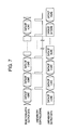
- FIG. 7 is an explanatory diagram for explaining the operation of the line memory
- FIG. 8 is a detailed configuration diagram of the scanning circuit.
- FIG. 9 is a configuration diagram of a second embodiment of the present invention.
- FIG. 3 illustrates a circuit configuration of a first embodiment of the liquid crystal display apparatus.
- the circuit includes, a data driver circuit 307 including a high-speed data bus 203 and low-speed data buses 102 divided into blocks, a scan driver circuit 210 , and a pixel unit 209 including active matrix pixels constituted by thin film transistors. These circuits are formed by the CMOSTET fabricating process on a glass substrate 305 of the display apparatus.
- a substrate on which the above-mentioned circuits are formed can be fabricated by using the following processes.
- a non-alkaline glass is employed as a glass substrate.
- the substrate is realized by a low temperature poly-Si TFT fabricating process which includes a process of poly-crystallizing an Si film constituting CMOS FETs by using laser-anneal crystallization and a doping process of obtaining n-type Si and p-type Si.
- a quartz substrate may be employed.
- the substrate may be realized by a high-temperature poly-Si process in which a poly-Si film is formed by using solid phase crystallization.
- Display data and synchronization signals necessary for the display from input terminals 214 are supplied to high-speed bus driving circuits 306 .
- the high-speed bus driving circuits 306 are connected to the high-speed data bus 203 and a high-speed control bus 216 .
- the high-speed data bus 203 and the high-speed control bus 216 are connected in sequence to high-speed data control circuits 104 and high-speed data rearranging circuits 101 , which are arranged on each block 103 , through the waveform shaping circuits 303 on the way to the data rearranging circuits.
- the display data are distributed in parallel onto the low-speed data buses 102 divided for the respective large numbers of blocks, then being connected to the respective latch circuits 302 in each block.
- the data rearranging circuits 101 expand the data in parallel in accordance with synchronization signals from the high-speed data control circuits 104 .
- the synchronization signals within the blocks are generated by the high-speed data control circuits 104 from the synchronization signals on the high-speed control bus 216 , then being supplied to the blocks by low-speed control buses 107 divided for the respective blocks.
- Within each block in correspondence with signal lines 208 of the pixel unit 209 , there are provided a plurality of shift registers 301 , the plurality of data latch circuits 302 , a plurality of line memories 205 , a plurality of level shifters 206 , and a plurality of D/A converting circuits 207 .
- the scan driver circuit 210 Based on a synchronization signal supplied by a panel scanning control bus 304 , the scan driver circuit 210 generates a scanning pulse needed for a line sequence scanning of the pixel unit 209 , then supplying the scanning pulse to scanning lines 213 of the pixel unit.
- the present circuit performs the display operation in the following manner:
- a dot clock, horizontal synchronization and vertical synchronization signals and the display data undergo a low impedance transformation and a level shift processing performed by the high-speed bus driving circuits 306 . After that, they are supplied to the high-speed data bus 203 and the high-speed control bus 216 , then being supplied to the respective blocks.
- the level shift processing adjusts amplitudes of the logical signals so that they may be fitted to the logical circuits including the CMOSTFTs.
- the waveform shaping circuits 303 located on the way correct a waveform distortion and a shift in timing between the data and the synchronization signals occurring during the bus transmission.
- the corresponding high-speed data control circuit 104 In connection with the respective blocks, from the dot clock and the horizontal synchronization signal on the high-speed control bus, the corresponding high-speed data control circuit 104 detects a time-period during which the data needed for the processing in the corresponding block has been reaching, then connecting the corresponding data rearranging circuit 101 to the high-speed data bus. In accordance with a control signal from the high-speed data control circuit 104 , the data rearranging circuit 101 executes an operation of rearranging in parallel the data on the high-speed data bus onto the low-speed data buses 102 .
- the wiring number of the low-speed data bus is constituted to be larger than at least the wiring number of the high-speed data bus.
- the shift registers 301 which operate in synchronization with the parallel rearranging operation, cause the latch circuits 302 to generate data latch signals in sequence. Then, the latch circuits 302 latch the display data on the low-speed data buses 102 , thereby transferring, to the latch circuits 302 , the display data corresponding to the corresponding block 103 .
- the respective blocks perform the above-described operation in sequence.
- the latch circuits transfer the data to the line memories 205 .
- the display data after being converted into a liquid crystal driving voltage by the D/A converting circuits, drive the signal wirings 208 so as to drive the pixel unit 209 .
- the scan driver circuit 210 drives the scanning wirings 213 of the pixel unit 209 , thereby making it possible to perform the display operation.
- increasing the number of wirings of the low-speed data bus results in an increase in the occupation area of the wirings and thus an increase in the circuit area. This situation requires that the number of wirings be optimized.
- the high-speed data rearranging circuits that are equal to the blocks in number are connected to the high-speed data bus.
- the number of the blocks is 8, octal data latches are connected per data line, and it is possible to reduce, down to ⁇ fraction (1/80) ⁇ th, the number of the load circuits to be connected to the high-speed data bus. Accordingly, when comparing the wiring time constants under the same condition, ⁇ fraction (1/80) ⁇ th of the wiring width turns out to be sufficient. This makes it possible to reduce the area of the wiring portion.
- FIG. 4 and FIG. 5 illustrate the content configuration of the high-speed data rearranging circuit 101 and that of the high-speed data control circuit 104 , both of which are the main components in the present invention.
- the high-speed control bus 216 includes a dot clock bus 401 and a horizontal start signal bus 402 .
- the high-speed data control circuit 104 includes a dot counter 403 and a decoder circuit 404 .
- the dot counter 403 includes a 9-bit binary counter that, with the dot clock employed as a clock, operates with a rising edge of the horizontal start signal employed as a count start signal and with a falling edge thereof employed as a reset signal.
- Combination of b 8 to b 0 i.e., the respective bit outputs 410 of the dot counter 403 , indicates a pixel position of the display data on respective scan the line that appears on the high-speed data bus not illustrated here.
- the decoder circuit 404 constituted using logical circuits generate the following necessary control signals from the bit outputs 410 of the dot counter 403 .
- a block selection signal 405 outputs an output of a logic “1” for a time-period during which the pixel data contained in the respective blocks are being outputted to the display data buses. In this case, it will do to decode b 8 to b 6 , i.e., higher-order 3 bits of the counter outputs. It will do to set the states of the higher-order 3 bits to be as follows: (0 0 0) in the 1st block, (0 0 1) in the 2nd block, (0 1 1) in the 3rd block, and (1 1 1) in the 8th block.
- the block selection signal is “1” when the states of the b 8 or b 6 is (0/0).
- the outputs b 5 to b 0 are provided with a switch 409 .
- the switch 409 is controlled so that the following signals are outputted only when the block selection signal is “1”. This prevents unnecessary operations of the logical circuits, thereby reducing the power consumption of the decoder circuit 404 .
- a low-speed start signal 406 is outputted for a time from a time-period when a pixel at the left end within the block to a 4-clock time-period. This signal is obtained by executing the NAND operation toward the case where all of b 5 to b 2 are 0.
- 4-phase low-speed shift clocks 407 i.e., # 1 to # 4 are generated using b 1 and b 0 .
- # 1 and # 3 are an inverted signal of b 1 and that of b 1 , respectively, and # 2 is obtained by executing the EX-OR operation toward b 1 and b 0 .
- # 4 an inverted signal of # 2 is employed.
- 4 low-speed bus switching signals 408 can be generated by decoding b 0 and b 1 .
- the dot counter 403 is reset for each horizontal period by the falling edge of the horizontal start pulse, and then the above-described operation is repeated for each line.
- a function of the high-speed data rearranging circuit 101 is to expand in n-parallel the signals on the high-speed data bus onto the low-speed data buses 102 , the number of which is constituted to be n times that of the high-speed data bus 203 .
- This function results in an advantage of prolong a display data processing time ranging from the data latch to the D/A converting processing for each pixel and of allowing the inputted display data to be dealt with at a high transfer rate even if the wiring response is slow.
- the respective wirings constituting the high-speed data bus 203 are connected to a bus driving circuit 502 through block selection switches 501 , the electrical conductions of which are controlled in common on a block basis by the block selection signal 405 .
- This causes the bus driving circuit to be connected to the high-speed data bus wirings as the load only when the block selection switches are brought into conduction states, or turned on by the block selection signal.
- Outputs of the bus driving circuit have a function of switching the connection from a signal on 1 line of the high-speed data bus to a signal on 4 lines of the low-speed data buses.
- the bus driving circuit is of a selector circuit configuration constituted by 4 units of CMOS analogue switches, and is connected to low-speed bus switching switches 503 controlled by the low-speed bus switching signals.
- the bus driving circuit is of a selector circuit configuration constituted by 4 units of CMOS analogue switches, and is connected to low-speed bus switching switches 503 controlled by the low-speed bus switching signals.
- there exist 4 lines of the low-speed data buses toward 1 line of the high-speed data bus. Accordingly, in order to achieve the 6-bit gray shade display for each pixel, it is necessary to use 6 ⁇ 4 lines 24 lines of the low-speed data buses.
- the large numbers of data latch circuits and parastic capacitors 504 which are formed by intersection portions of the wirings, are formed on the low-speed data buses. This condition allows the voltages of the low-speed data bus wirings to be maintained even when the low-speed bus switching switches are cut off.
- the block selection switches 501 and the low-speed bus switching switches 503 can be implemented by the combination of appropriate
- FIG. 6 illustrates the operation waveforms in the respective portions of the high-speed data control circuit 104 and the high-speed data rearranging circuit 101 , which execute the signal converting processing from the high-speed data bus to the low-speed data buses.
- n units of blocks each of which includes m pixels and 4 lines of the low-speed data buses per bit within each block.
- On the high-speed data bus there appear in sequence the display data from 1 to (m ⁇ n) pixels, i.e., the pixels by the amount of one scan line, in synchronization with the horizontal synchronization signal with positive polarity.
- the block selection signal in the respective blocks becomes a positive logic for only a time-period during which the data equivalent to the respective blocks appear, thereby turning on the block selection switches 405 into the conduction states so as to connect the high-speed data bus 203 to the bus driving circuit 502 .
- the operation of the high-speed data rearranging circuit 101 will be explained concerning the 2nd block including (m+1) to 2m pixels.
- the high-speed data rearranging circuit 101 is caused to synchronize the high-speed dot clock by the high-speed data control circuit 104 .
- the low-speed bus switching switches 503 connect the respective bits onto 4 lines of the low-speed data buses.
- the data at 4-pixel intervals are fetched onto the low-speed data buses in such a manner that the data in (m+1) and (m+5) pixels are fetched onto the bus of # 1 and the data in (m+2) and (m+6) pixels are fetched onto the bus of # 2.
- the data on the low-speed data buses are updated every 4 pixels in the following sequence: the data in (m+1) pixel on # 1, the data in (m+2) pixel on # 2, the data in (m+3) pixel on # 3, the data in (m+4) pixel on # 4, the data in (m+5) pixel on # 1, and the data in (m+6) pixel on # 2.
- the serial data in the 1-pixel sequence which have been transferred by 1 line of the high-speed data bus, are distributed on the low-speed data buses in the parallel form at 4-pixel intervals.
- 4-phase shift registers are employed as the shift registers 301 within the respective blocks.
- 4-phase clocks for driving the 4-phase shift registers are generated as the low-speed shift clocks by the high-speed data control circuit 104 .
- the period of the low-speed shift clocks is equal to 4 periods of the high-speed dot clock and the phases thereof are delayed to each other by 1 clock, as is the case with the low-speed bus switching signals.
- Outputs of the respective stages of the shift registers become latch signals for driving the data latches 302 in FIG. 3 .
- the latch signals have become pulses, the pulse width of which is equal to 4 periods of the high-speed dot clock and which are delayed to each other by 1 clock.
- the respective data latches are connected to outputs of the respective line memories, and the data by the amount of one scanning line are updated for each horizontal time-period.
- the line memories fetch the data to be inputted after being updated, then updating the data.
- the updated data are connected to the respective D/A converting circuits 207 in FIG. 3 and are converted into the liquid crystal driving voltage instantaneously, then being supplied to the signal lines 208 for driving the pixel unit 209 .
- the operation waveforms of the pixel unit are the same as those in conventional configuration, and accordingly will be explained briefly. A configuration of a circuit is illustrated in FIG.
- the shift registers 801 drive the circuit, taking advantage of the shift clock with a period of one horizontal time-period and a pulse of the frame start signal for each frame time.
- the circuit applies scanning pulses, which are shifted in sequence for each period of one horizontal time-period, to the scanning lines 213 in FIG. 3 through the level shifters and the data driver circuit 802 .
- the D/A converting circuits apply the liquid crystal driving voltage in each dot to the respective signal wirings by the amount of one line in synchronization with the scanning pulses, thereby performing the display by the pixels.
- the diagram illustrates the circuit configuration of each block.
- a characteristic of the system lies in a point of transferring the latches from the data latches to the memories with timings that are different for the respective blocks.
- another characteristic lies in a point of performing the data transfer from the line memories to the D/A converting circuits with timings that are different for the respective blocks.
- a memory selecting switch 901 is provided between the latch circuits and the memory circuits and a D/A converting circuit selecting switch 902 is provided between the line memories and the D/A converting circuits, and the switch 901 and the switch 902 are controlled by a memory transferring signal 903 and a D/A conversion transferring signal 904 , respectively.
- the memory selecting switch and the D/A selecting switch are configured by employing CMOS analogue switches 905 by the number of the lines, and in addition inverters 906 are employed in order to obtain control signals with both polarities for driving the analogue switches.
- the control signals for driving the analogue switches are connected in common, thereby collectively controlling the analogue switches by the number of one block with the use of the respective transferring signals 903 , 904 .
- This configuration allows the operations of the line memory circuits to be dispersed for each block, thus resulting in an advantage of being able to disperse the power consumption and decrease the capacitance of the power supply circuit.
- the D/A converting circuits are driven in a state of being divided for each block, thereby making it possible to disperse in time the power supply current of the D/A converting circuits. This results in an advantage of being able not only to reduce the power consumption but also to obtain a liquid crystal driving voltage that is stable and exhibits a less error even if the wiring resistance is high. The reason for the latter is that it is possible to reduce a voltage drop in the power supply wiring.
- the high-speed data buses and the high-speed control buses formed on the display TFT substrate supply the synchronization signals, such as the high-speed display data and the dot clock both of which are supplied from the outside, to the terminal end of the data driver circuit through the waveform shaping circuits.
- the display data are distributed in parallel onto the large numbers of low-speed data buses separated for each block, then being fetched at a low transfer rate into the respective data latches within each block. After that, by being transferred to the respective line memories, the display data by the amount of one line are latched therein. Taking advantage of the data, the digital gray shade data in each dot are converted into the gray shade voltage to be applied to the liquid crystal of the pixels.
- Transferring the display data to the large numbers of the data latches in this way permits the display data to be transferred as a whole to the peripheral circuit on the large-sized panel at a high transfer rate, thus making it possible to easily configure the large-sized high-resolution panel.
- the liquid crystal display apparatus exhibits only a small load capacitance on the display panel, and even in the large-sized high-resolution panel, allows the display data inputted into the high-speed data buses to be transmitted up to the terminal ends of the data buses with a small waveform distortion.
Landscapes
- Engineering & Computer Science (AREA)
- Computer Networks & Wireless Communication (AREA)
- Signal Processing (AREA)
- Chemical & Material Sciences (AREA)
- Crystallography & Structural Chemistry (AREA)
- Physics & Mathematics (AREA)
- Computer Hardware Design (AREA)
- General Physics & Mathematics (AREA)
- Theoretical Computer Science (AREA)
- Liquid Crystal Display Device Control (AREA)
- Control Of Indicators Other Than Cathode Ray Tubes (AREA)
- Liquid Crystal (AREA)
Abstract
Description
Claims (9)
Applications Claiming Priority (2)
| Application Number | Priority Date | Filing Date | Title |
|---|---|---|---|
| JP11-049619 | 1999-02-26 | ||
| JP04961999A JP3622559B2 (en) | 1999-02-26 | 1999-02-26 | Liquid crystal display |
Publications (1)
| Publication Number | Publication Date |
|---|---|
| US6825826B1 true US6825826B1 (en) | 2004-11-30 |
Family
ID=12836263
Family Applications (1)
| Application Number | Title | Priority Date | Filing Date |
|---|---|---|---|
| US09/511,160 Expired - Lifetime US6825826B1 (en) | 1999-02-26 | 2000-02-23 | Liquid crystal display apparatus |
Country Status (4)
| Country | Link |
|---|---|
| US (1) | US6825826B1 (en) |
| JP (1) | JP3622559B2 (en) |
| KR (1) | KR100713185B1 (en) |
| TW (1) | TW511044B (en) |
Cited By (15)
| Publication number | Priority date | Publication date | Assignee | Title |
|---|---|---|---|---|
| US20020109659A1 (en) * | 2001-02-08 | 2002-08-15 | Semiconductor Energy Laboratory Co.,Ltd. | Liquid crystal display device, and method of driving the same |
| US20030179171A1 (en) * | 2002-03-05 | 2003-09-25 | Seiko Epson Corporation | Display driver circuit and display panel including the same |
| US20040189564A1 (en) * | 2003-03-28 | 2004-09-30 | Masami Makuuchi | Semiconductor device and testing method of semiconductor device |
| US20050073526A1 (en) * | 2003-10-02 | 2005-04-07 | Nec Electronics Corporation | Controller/driver for driving display panel |
| US20050146494A1 (en) * | 2003-12-08 | 2005-07-07 | Yoshinori Aoki | Liquid crystal display device |
| US20060202926A1 (en) * | 2005-03-08 | 2006-09-14 | Sanyo Epson Imaging Devices Corp. | Semiconductor circuit, driving circuit of electro-optical device, and electronic apparatus |
| US20070132702A1 (en) * | 2005-12-08 | 2007-06-14 | Noriyuki Kajihara | Display driving integrated circuit and method for determining wire configuration of the same |
| US20070146287A1 (en) * | 2005-12-27 | 2007-06-28 | Lg Philips Lcd Co., Ltd. | Apparatus and method for driving LCD |
| US20080079707A1 (en) * | 2006-09-29 | 2008-04-03 | Kazuya Matsumoto | Signal transfer circuit, display data processing apparatus, and display apparatus |
| US20080218229A1 (en) * | 2006-06-22 | 2008-09-11 | International Business Machines Corporation | Adjustment of pll bandwidth for jitter control using feedback circuitry |
| US20080231573A1 (en) * | 2000-07-25 | 2008-09-25 | Mitsuru Goto | Liquid Crystal Display Device |
| US20080252576A1 (en) * | 2007-04-16 | 2008-10-16 | Novatek Microelectronics Corp. | Panel display apparatus and source driver thereof |
| US20090033644A1 (en) * | 2007-08-03 | 2009-02-05 | Sony Corporation | Display device and wiring routing method |
| US10937779B2 (en) * | 2004-07-05 | 2021-03-02 | 138 East LCD Advancement Limited | Semiconductor device, display device, and electronic apparatus |
| US11062641B2 (en) * | 2018-11-07 | 2021-07-13 | Canon Kabushiki Kaisha | Display device and image capturing device |
Families Citing this family (5)
| Publication number | Priority date | Publication date | Assignee | Title |
|---|---|---|---|---|
| JP4139719B2 (en) | 2003-03-31 | 2008-08-27 | シャープ株式会社 | Liquid crystal display |
| JP4599808B2 (en) * | 2003-05-12 | 2010-12-15 | セイコーエプソン株式会社 | Electro-optical panel drive circuit, and electro-optical device and electronic apparatus including the same |
| KR101314324B1 (en) * | 2006-11-30 | 2013-10-02 | 엘지디스플레이 주식회사 | FSC mode liquid crystal display driving circuit and driving method thereof |
| JP5211591B2 (en) * | 2007-09-10 | 2013-06-12 | セイコーエプソン株式会社 | Data line driving circuit, electro-optical device, and electronic apparatus |
| CN102646385B (en) * | 2012-05-04 | 2014-10-08 | 中国科学院苏州纳米技术与纳米仿生研究所 | Drive circuit structure of spatial light modulator |
Citations (2)
| Publication number | Priority date | Publication date | Assignee | Title |
|---|---|---|---|---|
| US6222518B1 (en) * | 1993-08-30 | 2001-04-24 | Hitachi, Ltd. | Liquid crystal display with liquid crystal driver having display memory |
| US6268841B1 (en) * | 1998-01-09 | 2001-07-31 | Sharp Kabushiki Kaisha | Data line driver for a matrix display and a matrix display |
Family Cites Families (4)
| Publication number | Priority date | Publication date | Assignee | Title |
|---|---|---|---|---|
| JP3243178B2 (en) * | 1995-04-27 | 2002-01-07 | キヤノン株式会社 | Data transfer method and display device using the same |
| JP3526992B2 (en) * | 1995-11-06 | 2004-05-17 | 株式会社半導体エネルギー研究所 | Matrix type display device |
| TW373115B (en) * | 1997-02-07 | 1999-11-01 | Hitachi Ltd | Liquid crystal display device |
| TW440742B (en) * | 1997-03-03 | 2001-06-16 | Toshiba Corp | Flat panel display device |
-
1999
- 1999-02-26 JP JP04961999A patent/JP3622559B2/en not_active Expired - Fee Related
-
2000
- 2000-01-11 TW TW089100360A patent/TW511044B/en not_active IP Right Cessation
- 2000-02-23 US US09/511,160 patent/US6825826B1/en not_active Expired - Lifetime
- 2000-02-25 KR KR1020000009311A patent/KR100713185B1/en not_active Expired - Fee Related
Patent Citations (2)
| Publication number | Priority date | Publication date | Assignee | Title |
|---|---|---|---|---|
| US6222518B1 (en) * | 1993-08-30 | 2001-04-24 | Hitachi, Ltd. | Liquid crystal display with liquid crystal driver having display memory |
| US6268841B1 (en) * | 1998-01-09 | 2001-07-31 | Sharp Kabushiki Kaisha | Data line driver for a matrix display and a matrix display |
Cited By (33)
| Publication number | Priority date | Publication date | Assignee | Title |
|---|---|---|---|---|
| US9372375B2 (en) | 2000-07-25 | 2016-06-21 | Japan Display Inc. | Liquid crystal display device |
| US8299997B2 (en) * | 2000-07-25 | 2012-10-30 | Hitachi Displays, Ltd. | Liquid crystal display device |
| US20080231573A1 (en) * | 2000-07-25 | 2008-09-25 | Mitsuru Goto | Liquid Crystal Display Device |
| US7535448B2 (en) * | 2001-02-08 | 2009-05-19 | Semiconductor Energy Laboratory Co., Ltd. | Liquid crystal display device, and method of driving the same |
| US20020109659A1 (en) * | 2001-02-08 | 2002-08-15 | Semiconductor Energy Laboratory Co.,Ltd. | Liquid crystal display device, and method of driving the same |
| US20030179171A1 (en) * | 2002-03-05 | 2003-09-25 | Seiko Epson Corporation | Display driver circuit and display panel including the same |
| US6980187B2 (en) * | 2002-03-05 | 2005-12-27 | Seiko Epson Corporation | Display driver circuit and display panel including the same |
| US20040189564A1 (en) * | 2003-03-28 | 2004-09-30 | Masami Makuuchi | Semiconductor device and testing method of semiconductor device |
| US20050073526A1 (en) * | 2003-10-02 | 2005-04-07 | Nec Electronics Corporation | Controller/driver for driving display panel |
| US7327342B2 (en) * | 2003-10-02 | 2008-02-05 | Nec Electronics Corporation | Controller/driver for driving display panel |
| US20050146494A1 (en) * | 2003-12-08 | 2005-07-07 | Yoshinori Aoki | Liquid crystal display device |
| US20090267931A1 (en) * | 2003-12-08 | 2009-10-29 | Yoshinori Aoki | Liquid Crystal Display Device |
| US7602366B2 (en) * | 2003-12-08 | 2009-10-13 | Hitachi Displays, Ltd. | Liquid crystal display device |
| US10937779B2 (en) * | 2004-07-05 | 2021-03-02 | 138 East LCD Advancement Limited | Semiconductor device, display device, and electronic apparatus |
| US11362081B2 (en) | 2004-07-05 | 2022-06-14 | 138 East Lcd Advancements Limited | Semiconductor device, display device, and electronic apparatus |
| US20220310588A1 (en) * | 2004-07-05 | 2022-09-29 | 138 East Lcd Advancements Limited | Semiconductor device, display device, and electronic apparatus |
| US11955473B2 (en) * | 2004-07-05 | 2024-04-09 | 138 East Lcd Advancements Limited | Semiconductor device, display device, and electronic apparatus |
| US8537152B2 (en) | 2005-03-08 | 2013-09-17 | Epson Imaging Devices Corporation | Semiconductor circuit, driving circuit of electro-optical device, and electronic apparatus |
| US20110037754A1 (en) * | 2005-03-08 | 2011-02-17 | Epson Imaging Devices Corporation | Semiconductor circuit, driving circuit of electro-optical device, and electronic apparatus |
| US20060202926A1 (en) * | 2005-03-08 | 2006-09-14 | Sanyo Epson Imaging Devices Corp. | Semiconductor circuit, driving circuit of electro-optical device, and electronic apparatus |
| US7847759B2 (en) * | 2005-03-08 | 2010-12-07 | Epson Imaging Devices Corporation | Semiconductor circuit, driving circuit of electro-optical device, and electronic apparatus |
| US8552935B2 (en) * | 2005-03-08 | 2013-10-08 | Epson Imaging Devices Corporation | Semiconductor circuit, driving circuit of electro-optical device, and electronic apparatus |
| US9262985B2 (en) | 2005-03-08 | 2016-02-16 | Epson Imaging Devices Corporation | Semiconductor circuit, driving circuit of electro-optical device, and electronic apparatus |
| US20070132702A1 (en) * | 2005-12-08 | 2007-06-14 | Noriyuki Kajihara | Display driving integrated circuit and method for determining wire configuration of the same |
| US20070146287A1 (en) * | 2005-12-27 | 2007-06-28 | Lg Philips Lcd Co., Ltd. | Apparatus and method for driving LCD |
| US7999778B2 (en) * | 2005-12-27 | 2011-08-16 | Lg Display Co., Ltd. | Apparatus and method for driving LCD |
| KR101284940B1 (en) * | 2005-12-27 | 2013-07-10 | 엘지디스플레이 주식회사 | Apparatus and method for driving a liquid crystal display |
| US20080218229A1 (en) * | 2006-06-22 | 2008-09-11 | International Business Machines Corporation | Adjustment of pll bandwidth for jitter control using feedback circuitry |
| US20080079707A1 (en) * | 2006-09-29 | 2008-04-03 | Kazuya Matsumoto | Signal transfer circuit, display data processing apparatus, and display apparatus |
| US20080252576A1 (en) * | 2007-04-16 | 2008-10-16 | Novatek Microelectronics Corp. | Panel display apparatus and source driver thereof |
| US8379003B2 (en) * | 2007-08-03 | 2013-02-19 | Sony Corporation | Display device and wiring routing method |
| US20090033644A1 (en) * | 2007-08-03 | 2009-02-05 | Sony Corporation | Display device and wiring routing method |
| US11062641B2 (en) * | 2018-11-07 | 2021-07-13 | Canon Kabushiki Kaisha | Display device and image capturing device |
Also Published As
| Publication number | Publication date |
|---|---|
| KR20000062639A (en) | 2000-10-25 |
| TW511044B (en) | 2002-11-21 |
| KR100713185B1 (en) | 2007-05-02 |
| JP3622559B2 (en) | 2005-02-23 |
| JP2000250010A (en) | 2000-09-14 |
Similar Documents
| Publication | Publication Date | Title |
|---|---|---|
| US6825826B1 (en) | Liquid crystal display apparatus | |
| KR100229380B1 (en) | Driving circuit of liquid crystal display panel using digital method | |
| US6630920B1 (en) | Pel drive circuit, combination pel-drive-circuit/pel-integrated device, and liquid crystal display device | |
| EP0861484B1 (en) | Lcd driver ic with pixel inversion operation | |
| US8072404B2 (en) | Liquid crystal display device | |
| US6157358A (en) | Liquid crystal display | |
| KR100367387B1 (en) | High density column drivers for an active matrix display | |
| US20090219240A1 (en) | Liquid crystal display driver device and liquid crystal display system | |
| KR19990029652A (en) | Liquid crystal display element | |
| US5621426A (en) | Display apparatus and driving circuit for driving the same | |
| US6437775B1 (en) | Flat display unit | |
| US4785297A (en) | Driver circuit for matrix type display device | |
| JP4175058B2 (en) | Display drive circuit and display device | |
| KR100372847B1 (en) | Semiconductor device and display module | |
| US7042433B1 (en) | Signal line driving circuit and image display device | |
| JP2000162577A (en) | Flat display device, array substrate, and method of driving flat display device | |
| KR100227293B1 (en) | Scanning circuit and image display device | |
| JP3755360B2 (en) | Drive circuit for electro-optical device, electro-optical device using the same, electronic apparatus, phase adjusting device for control signal of electro-optical device, and phase adjusting method for control signal | |
| KR100582381B1 (en) | Image data compression transmission method performed in source driver and driver | |
| JP3669514B2 (en) | Driving circuit for liquid crystal display device | |
| US20080122810A1 (en) | Flat Display Unit | |
| JP2000122616A (en) | Liquid crystal display device with switch circuit | |
| JPS6148893A (en) | Active matrix panel with built-in driver | |
| JP4854129B2 (en) | Display device | |
| JP3495745B2 (en) | Active matrix panel |
Legal Events
| Date | Code | Title | Description |
|---|---|---|---|
| AS | Assignment |
Owner name: HITACHI, LTD., JAPAN Free format text: ASSIGNMENT OF ASSIGNORS INTEREST;ASSIGNORS:MIKAMI, YOSHIRO;SATO, HIDEO;KAGEYAMA, HIROSHI;AND OTHERS;REEL/FRAME:010799/0799;SIGNING DATES FROM 20000402 TO 20000420 |
|
| STCF | Information on status: patent grant |
Free format text: PATENTED CASE |
|
| FEPP | Fee payment procedure |
Free format text: PAYOR NUMBER ASSIGNED (ORIGINAL EVENT CODE: ASPN); ENTITY STATUS OF PATENT OWNER: LARGE ENTITY |
|
| FPAY | Fee payment |
Year of fee payment: 4 |
|
| AS | Assignment |
Owner name: PANASONIC LIQUID CRYSTAL DISPLAY CO., LTD., JAPAN Free format text: MERGER/CHANGE OF NAME;ASSIGNOR:IPS ALPHA SUPPORT CO., LTD.;REEL/FRAME:027363/0315 Effective date: 20101001 Owner name: HITACHI DISPLAYS, LTD., JAPAN Free format text: COMPANY SPLIT PLAN TRANSFERRING ONE HUNDRED (100) PERCENT SHARE OF PATENT AND PATENT APPLICATIONS;ASSIGNOR:HITACHI, LTD.;REEL/FRAME:027362/0612 Effective date: 20021001 Owner name: IPS ALPHA SUPPORT CO., LTD., JAPAN Free format text: COMPANY SPLIT PLAN TRANSFERRING FIFTY (50) PERCENT SHARE OF PATENTS AND PATENT APPLICATIONS;ASSIGNOR:HITACHI DISPLAYS, LTD.;REEL/FRAME:027362/0466 Effective date: 20100630 |
|
| FPAY | Fee payment |
Year of fee payment: 8 |
|
| FPAY | Fee payment |
Year of fee payment: 12 |