US6806129B1 - Self-aligned process using indium gallium arsenide etching to form reentry feature in heterojunction bipolar transistors - Google Patents
Self-aligned process using indium gallium arsenide etching to form reentry feature in heterojunction bipolar transistors Download PDFInfo
- Publication number
- US6806129B1 US6806129B1 US10/435,230 US43523003A US6806129B1 US 6806129 B1 US6806129 B1 US 6806129B1 US 43523003 A US43523003 A US 43523003A US 6806129 B1 US6806129 B1 US 6806129B1
- Authority
- US
- United States
- Prior art keywords
- layer
- forming
- emitter
- exposed portion
- collector
- Prior art date
- Legal status (The legal status is an assumption and is not a legal conclusion. Google has not performed a legal analysis and makes no representation as to the accuracy of the status listed.)
- Expired - Fee Related
Links
Images


Classifications
-
- H—ELECTRICITY
- H10—SEMICONDUCTOR DEVICES; ELECTRIC SOLID-STATE DEVICES NOT OTHERWISE PROVIDED FOR
- H10D—INORGANIC ELECTRIC SEMICONDUCTOR DEVICES
- H10D10/00—Bipolar junction transistors [BJT]
- H10D10/01—Manufacture or treatment
- H10D10/021—Manufacture or treatment of heterojunction BJTs [HBT]
-
- H—ELECTRICITY
- H10—SEMICONDUCTOR DEVICES; ELECTRIC SOLID-STATE DEVICES NOT OTHERWISE PROVIDED FOR
- H10D—INORGANIC ELECTRIC SEMICONDUCTOR DEVICES
- H10D10/00—Bipolar junction transistors [BJT]
- H10D10/80—Heterojunction BJTs
- H10D10/821—Vertical heterojunction BJTs
-
- H—ELECTRICITY
- H10—SEMICONDUCTOR DEVICES; ELECTRIC SOLID-STATE DEVICES NOT OTHERWISE PROVIDED FOR
- H10D—INORGANIC ELECTRIC SEMICONDUCTOR DEVICES
- H10D62/00—Semiconductor bodies, or regions thereof, of devices having potential barriers
- H10D62/80—Semiconductor bodies, or regions thereof, of devices having potential barriers characterised by the materials
- H10D62/85—Semiconductor bodies, or regions thereof, of devices having potential barriers characterised by the materials being Group III-V materials, e.g. GaAs
Definitions
- This invention relates to a heterojunction bipolar transistor (HBT), and more specifically to a self-aligned process for fabricating emitter and base metals for a HBT that reduces base resistance.
- HBT heterojunction bipolar transistor
- a heterojunction bipolar transistor is a bipolar transistor having two adjacent layers of different materials.
- FIG. 1 illustrates a conventional HBT 10 .
- HBT 10 includes a collector 12 , a base 14 , an emitter 16 , and an emitter cap 18 .
- Emitter metal 22 and base metals 24 are typically made in a self-aligned process.
- reentry features 20 are formed in emitter 16 .
- Reentry features 20 are ledges, overhangs, and other features with an undercut profile.
- Reentry features 20 are formed by selectively wet etching emitter 16 .
- Metal is then deposited on cap 18 and base 14 to form emitter metal 22 and base metals 24 , respectively.
- Reentry features 20 create breaks in emitter metal 22 and base metals 24 so they are not electrically shorted.
- One of the goals in designing an HBT is to minimize the base resistance, which is the resistance between emitter 16 and base metal 24 through base 14 .
- One way to minimize the base resistance is to reduce a distance D between emitter 16 and base metal 24 . Distance D can be reduced by controlling the shape of reentry features 20 .
- reentry features 20 can be formed by selectively wet etching emitter 16 underneath a photoresist.
- FIGS. 2A and 2B illustrate a wet etch of an InP (indium phosphide) emitter 16 underneath a photoresist 21 in a direction perpendicular to the (100) wafer flat. This wet etch forms ledges in the InP emitter 16 that can be used as reentry features 20 .
- FIG. 2B also shows a wet etch of an InGaAs (indium gallium arsenide) cap 18 underneath photoresist 21 . This wet etch forms ramps 23 in the InGaAs cap 18 that cannot be used as reentry features.
- InP indium phosphide
- FIG. 2B also shows a wet etch of an InGaAs (indium gallium arsenide) cap 18 underneath photoresist 21 . This wet etch forms ramps 23 in the InGaAs cap
- FIGS. 2A and 2C illustrate a wet etch of the InP emitter 16 underneath photoresist 21 in a direction parallel to the (100) wafer flat. This wet etch forms ramps 26 in the InP emitter 16 that cannot be used as reentry features. However, ramps 26 can be used as means to run metal lines up to the top layer.
- FIG. 3A illustrates a wet etching of the InP emitter 16 underneath photoresist 21 in a direction 45 degrees from the (100) wafer flat.
- This wet etch forms four ledges that can be used as reentry features 20 .
- precise alignment e.g., to less than one degree
- ramps and other shapes may form instead of ledges.
- FIG. 3B where a misalignment of the wafer causes the wet etch to form a ramp 28 underneath photoresist 21 instead of a ledge.
- FIG. 4 illustrates an HBT 30 having reentry features 32 formed by a combination of dry and wet etch of emitter 16 .
- a dry etch is first used to etch both cap 18 and emitter 16 to form vertical sidewalls down to base 14 .
- Emitter 16 is next wet etched underneath cap 18 to create overhangs that form reentry features 32 .
- dry etch is not selective and thus requires precise control to avoid etching into base 14 and causing irreversible damage to HBT 30 .
- a method for forming a heterojunction bipolar transistor includes forming an etch mask atop an emitter cap layer of the HBT to expose a portion of the emitter cap layer, and selectively etching the exposed portion of the emitter cap layer to (1) form a reentry feature and (2) to expose a portion of the emitter layer.
- the method further includes selectively etching the exposed portion of the emitter layer to expose a portion of the base layer, and forming a metal layer over the exposed portion of the base layer and the exposed portion of the emitter cap layer.
- FIGS. 1, 2 A, 2 B, 2 C, 3 A, 3 B, and 4 illustrate conventional heterojunction bipolar transistors.
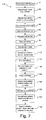
- FIG. 5 is a flowchart of a method for a self-aligned process to form metal contacts in an HBT in accordance with one aspect of the invention.
- FIGS. 6A, 6 B, 6 C, 6 D, 6 E, and 6 F are cross-sections of an HBT formed by the method of FIG. 5 in one embodiment of the invention.
- FIG. 7 is a flowchart of a method for a self-aligned process to form metal contacts in an HBT in accordance with another aspect of the invention.
- FIGS. 8A, 8 B, 8 C, and 8 D are cross-sections of an HBT formed by the method of FIG. 7 in one embodiment of the invention.
- an etch mask is used to selectively etch an emitter cap, instead of the emitter, in a heterojunction bipolar transistor to form reentry features for metal deposition.
- the reentry features allow metal contacts to self-align on the emitter cap and the base during metal deposition.
- FIG. 5 is a flowchart of a method 50 to form reentry features in one embodiment of the invention.
- the basic HBT layers are formed as shown in FIG. 6 A.
- the basic HBT layers include a substrate 92 , a sub-collector layer 94 A, a collector layer 112 A, a base layer 114 A, an emitter layer 116 A, and an emitter cap layer 118 A.
- Substrate 92 and sub-collector layer 94 A are typically InP (indium phosphide), collector layer 112 A are typically InGaAs (indium gallium arsenide) or InP, base layer 114 A is typically InGaAs or GaAsSb (gallium arsenide antimony), emitter layer 116 A is typically InP or AlInAs (aluminum indium arsenide), and cap layer 118 A is typically InGaAs. These layers are appropriately doped to form an n-p-n or a p-n-p HBT. Additional, an AlInAs layer (not shown) can be inserted between the emitter and the base to improve device performance. In one embodiment, these layers are formed by OMVPE (organometallic vapor phase epitaxy).
- OMVPE organometallic vapor phase epitaxy
- an etch masking layer 96 is formed and patterned as shown in FIG. 6 B. Specifically, in step 54 , etch masking layer 96 is formed atop cap layer 118 A. The material of etch masking layer 96 is selected to produce a ledge or overhang in the InGaAs cap layer 118 A when cap layer 118 A is selectively etched underneath etch masking layer 96 . Thus, a photoresist cannot be used as an etch mask for the InGaAs cap layer 118 A as it would produce a sidewall that is a ramp instead of a ledge or overhang as shown in FIG. 2 B.
- etch masking layer 96 is made of nitride. Nitride can be formed by PECVD (plasma enhanced chemical vapor deposition). Alternatively, etch masking layer 96 is made of InP. InP can be grown by OMVPE.
- a photoresist layer 98 is deposited over the device area and patterned to expose a portion of etch masking layer 96 .
- the unexposed portion of etch masking layer 96 defines emitter 116 (shown later in FIG. 6 C).
- etch masking layer 96 is removed by a nitride etch.
- etch masking layer 96 is dry etched using reactive ion etching (RIE). Afterwards, photoresist 98 can be stripped from etch masking layer 96 .
- RIE reactive ion etching
- emitter cap 118 is formed as shown in FIG. 6 C.
- Cap 118 is formed by selectively etching cap layer 118 A, thereby forming sidewalls with reentry features 100 and exposing emitter layer 116 A.
- reentry features 100 are features with an undercut profile such as ledges and overhangs.
- cap layer 118 A is selectively etched by a wet etch using a solution of DI (de-ionized) water, H2SO4 (sulphuric acid), and hydrogen peroxide (e.g., at a 300:30:30 ratio).
- DI de-ionized
- H2SO4 sulphuric acid
- hydrogen peroxide e.g., at a 300:30:30 ratio
- emitter 116 is formed as shown in FIG. 6 C.
- Emitter 116 is formed by selectively etching emitter layer 116 A, thereby exposing base layer 114 A.
- emitter layer 116 A is selectively etched to produce a more vertical sidewall than cap layer 118 A.
- emitter layer 116 A is selectively etched by a wet etch using a solution of HCI (hydrochloric acid) and H3PO4 (phosphoric acid) (e.g., at a 1:3 or 3:2 ratio).
- step 64 etch masking layer 96 is stripped.
- base-collector mesa (including base 114 and collector 112 ) and sub-collector mesa (including sub-collector 94 ) are formed as shown in FIG. 6 D.
- Base-collector mesa is first formed by depositing and patterning a nitride mask or a photoresist to expose and etch away portions of base layer 114 A and collector layer 112 A.
- Sub-collector mesa is then formed by depositing and patterning a photoresist to expose and etch away portions of sub-collector layer 94 A.
- the sub-collector mesa can be formed before the base-collector mesa in some embodiments.
- sub-collector metal contacts 110 are formed as shown in FIG. 6 E.
- sub-collector metals 110 are formed by depositing and patterning a photoresist 108 to open windows 115 to sub-collector 94 , and depositing metal atop photoresist 108 and through windows 115 .
- Sub-collector metals 110 are typically Ti/Au or Ti/Pt/Au. Subsequently, photoresist layer 108 is stripped and the metal deposited thereon is lifted off.
- a photoresist layer 102 is deposited over the device and patterned to open a window 104 to cap 118 and base layer 14 A. Metal is deposited atop photoresist layer 102 and through window 104 to form emitter metal 22 and base metals 24 . In one embodiment, metal is evaporated onto cap 118 and base 114 using electron beam or thermal evaporator. Emitter metal 22 and base metals 24 are typically Ti/Au (titanium gold) or Ti/Pt/Au (titanium platinum gold). Subsequently, photoresist layer 102 is stripped and the metal deposited thereon is lifted off.
- another etch mask is used to selectively etch the base and the collector layers in the heterojunction bipolar transistor to form reentry features.
- the reentry features on the cap, base, and collector layers allow their respective metal contacts to be formed in a single metal deposition process.
- FIG. 7 is a flowchart of a method 140 in one embodiment of the invention.
- Method 140 includes steps 52 to 64 of method 50 that form the structure shown in FIG. 6 C. Step 64 is followed by a step 141 .
- a second etch masking layer 180 is formed and patterned using a photoresist 182 as shown in FIG. 8 A. Specifically, in step 141 , etch masking layer 180 is formed over the device. Etch masking layer 180 can be made of nitride. In one embodiment, etch masking layer 180 is formed by plasma enhanced chemical vapor deposition.
- step 142 photoresist layer 182 is deposited over the device and patterned to expose a portion of etch masking layer 180 .
- the unexposed portion of etch masking layer 180 defines base 114 (FIG. 8 B).
- etch masking layer 180 is dry etched using reactive ion etching (RTE). After the dry etch, photoresist 182 can be stripped from etch masking layer 180 .
- RTE reactive ion etching
- base 114 and collector 112 are formed as shown in FIG. 8 B.
- Base 114 and collector 112 are formed by selectively etching base layer 114 A and collector layer 112 A, thereby forming sidewalls with reentry features 184 and exposing sub-collector layer 94 A.
- base layer 114 A and collector layer 112 A are selectively etched by a wet etch. Wet etching base layer 114 A and collector layer 112 A also consistently produces reentry features due to the crystallographic nature of the wet etch with the nitride mask. This occurs in the same way as when cap 118 and emitter 116 were etched.
- steps 148 to 152 sub-collector 94 is formed as shown in FIG. 8 C. Specifically, in a step 148 , etch masking layer 180 is stripped.
- a photoresist 186 is deposited over the device and patterned to expose portions of sub-collector layer 94 A.
- step 152 the exposed portions of sub-collector layer 94 A are selectively etched to form trenches 187 to isolate the HBT from other devices.
- sub-collector layer 94 A is selectively etched by a wet etch.
- emitter metal 22 In steps 154 and 156 , emitter metal 22 , base metals 24 , and sub-collector metals 110 are formed as shown in FIG. 8 D. Specifically, in step 154 , a photoresist 188 is deposited over the device and patterned to open a window 190 to sub-collector 94 , base 114 , and cap 118 .
- metal is deposited atop photoresist 188 and through window 190 to form emitter metal 22 , base metals 24 , and sub-collector metals 110 in one step.
- metal is deposited by electron beam or thermal evaporation. These metals are typically Ti/Au or Ti/Pt/Au. Subsequently, photoresist layer 108 is stripped and the metal deposited thereon is lifted off.
- the above process can be modified to form a double HBT where the collector is made of InP instead of InGaAs.
- the InGaAs base is selectively etched but the InP collector will be time etched (either dry or wet) until the InP sub-collector is reached and metal can be deposited thereon.
- the base mesa includes only the base while the collector mesa includes the collector and the sub-collector.
Landscapes
- Bipolar Transistors (AREA)
- Electrodes Of Semiconductors (AREA)
Abstract
Description
Claims (12)
Priority Applications (4)
| Application Number | Priority Date | Filing Date | Title |
|---|---|---|---|
| US10/435,230 US6806129B1 (en) | 2003-05-09 | 2003-05-09 | Self-aligned process using indium gallium arsenide etching to form reentry feature in heterojunction bipolar transistors |
| US10/826,787 US20040224463A1 (en) | 2003-05-09 | 2004-04-16 | Self-aligned process using indium gallium arsenide etching to form reentry feature in heterojunction bipolar transistors |
| JP2004136266A JP2004336050A (en) | 2003-05-09 | 2004-04-30 | Self-alignment process for forming reentry shapes in heterojunction bipolar transistors |
| GB0410247A GB2402810B (en) | 2003-05-09 | 2004-05-07 | Heterojunction bipolar transistors |
Applications Claiming Priority (1)
| Application Number | Priority Date | Filing Date | Title |
|---|---|---|---|
| US10/435,230 US6806129B1 (en) | 2003-05-09 | 2003-05-09 | Self-aligned process using indium gallium arsenide etching to form reentry feature in heterojunction bipolar transistors |
Related Child Applications (1)
| Application Number | Title | Priority Date | Filing Date |
|---|---|---|---|
| US10/826,787 Division US20040224463A1 (en) | 2003-05-09 | 2004-04-16 | Self-aligned process using indium gallium arsenide etching to form reentry feature in heterojunction bipolar transistors |
Publications (2)
| Publication Number | Publication Date |
|---|---|
| US6806129B1 true US6806129B1 (en) | 2004-10-19 |
| US20040224460A1 US20040224460A1 (en) | 2004-11-11 |
Family
ID=32508043
Family Applications (2)
| Application Number | Title | Priority Date | Filing Date |
|---|---|---|---|
| US10/435,230 Expired - Fee Related US6806129B1 (en) | 2003-05-09 | 2003-05-09 | Self-aligned process using indium gallium arsenide etching to form reentry feature in heterojunction bipolar transistors |
| US10/826,787 Abandoned US20040224463A1 (en) | 2003-05-09 | 2004-04-16 | Self-aligned process using indium gallium arsenide etching to form reentry feature in heterojunction bipolar transistors |
Family Applications After (1)
| Application Number | Title | Priority Date | Filing Date |
|---|---|---|---|
| US10/826,787 Abandoned US20040224463A1 (en) | 2003-05-09 | 2004-04-16 | Self-aligned process using indium gallium arsenide etching to form reentry feature in heterojunction bipolar transistors |
Country Status (3)
| Country | Link |
|---|---|
| US (2) | US6806129B1 (en) |
| JP (1) | JP2004336050A (en) |
| GB (1) | GB2402810B (en) |
Cited By (1)
| Publication number | Priority date | Publication date | Assignee | Title |
|---|---|---|---|---|
| US20050199911A1 (en) * | 2004-03-10 | 2005-09-15 | Matsushita Electric Industrial Co., Ltd. | Semiconductor element and method for fabricating the same |
Families Citing this family (4)
| Publication number | Priority date | Publication date | Assignee | Title |
|---|---|---|---|---|
| KR100687758B1 (en) * | 2005-12-08 | 2007-02-27 | 한국전자통신연구원 | Heterojunction bipolar transistor and method for manufacturing same |
| TW200832725A (en) * | 2007-01-18 | 2008-08-01 | Univ Nat Central | Method of improving current distribution by non-uniform conductive layer |
| CN107958926B (en) * | 2017-11-22 | 2020-07-07 | 成都海威华芯科技有限公司 | A method for reworking the base pedestal in a heterojunction bipolar transistor device |
| CN109817701B (en) * | 2018-12-25 | 2022-05-10 | 泉州三安半导体科技有限公司 | Emitter structure of heterojunction bipolar transistor and thinning method of emitter |
Citations (6)
| Publication number | Priority date | Publication date | Assignee | Title |
|---|---|---|---|---|
| US5665614A (en) * | 1995-06-06 | 1997-09-09 | Hughes Electronics | Method for making fully self-aligned submicron heterojunction bipolar transistor |
| US5804487A (en) * | 1996-07-10 | 1998-09-08 | Trw Inc. | Method of fabricating high βHBT devices |
| US6310368B1 (en) * | 1998-07-02 | 2001-10-30 | Sharp Kabushiki Kaisha | Semiconductor device and method for fabricating same |
| US6376867B1 (en) * | 2000-08-03 | 2002-04-23 | Trw Inc. | Heterojunction bipolar transistor with reduced thermal resistance |
| US6406965B1 (en) | 2001-04-19 | 2002-06-18 | Trw Inc. | Method of fabricating HBT devices |
| US6605519B2 (en) * | 2001-05-02 | 2003-08-12 | Unaxis Usa, Inc. | Method for thin film lift-off processes using lateral extended etching masks and device |
Family Cites Families (6)
| Publication number | Priority date | Publication date | Assignee | Title |
|---|---|---|---|---|
| JPH0637100A (en) * | 1992-07-15 | 1994-02-10 | Sharp Corp | Manufacture of heterojunction bipolar transistor |
| FR2697945B1 (en) * | 1992-11-06 | 1995-01-06 | Thomson Csf | Process for etching a heterostructure of group III-V materials. |
| JP2001326229A (en) * | 2000-05-12 | 2001-11-22 | Toshiba Corp | Heterojunction bipolar transistor and manufacturing method thereof |
| KR100456037B1 (en) * | 2001-10-24 | 2004-11-15 | 한국과학기술원 | Method for fabricating Heterojunction Bipolar Transistor using lateral-reverse selective etching of collector |
| US6770919B2 (en) * | 2002-12-30 | 2004-08-03 | Xindium Technologies, Inc. | Indium phosphide heterojunction bipolar transistor layer structure and method of making the same |
| US6727530B1 (en) * | 2003-03-04 | 2004-04-27 | Xindium Technologies, Inc. | Integrated photodetector and heterojunction bipolar transistors |
-
2003
- 2003-05-09 US US10/435,230 patent/US6806129B1/en not_active Expired - Fee Related
-
2004
- 2004-04-16 US US10/826,787 patent/US20040224463A1/en not_active Abandoned
- 2004-04-30 JP JP2004136266A patent/JP2004336050A/en active Pending
- 2004-05-07 GB GB0410247A patent/GB2402810B/en not_active Expired - Fee Related
Patent Citations (7)
| Publication number | Priority date | Publication date | Assignee | Title |
|---|---|---|---|---|
| US5665614A (en) * | 1995-06-06 | 1997-09-09 | Hughes Electronics | Method for making fully self-aligned submicron heterojunction bipolar transistor |
| US5729033A (en) * | 1995-06-06 | 1998-03-17 | Hughes Electronics | Fully self-aligned submicron heterojunction bipolar transistor |
| US5804487A (en) * | 1996-07-10 | 1998-09-08 | Trw Inc. | Method of fabricating high βHBT devices |
| US6310368B1 (en) * | 1998-07-02 | 2001-10-30 | Sharp Kabushiki Kaisha | Semiconductor device and method for fabricating same |
| US6376867B1 (en) * | 2000-08-03 | 2002-04-23 | Trw Inc. | Heterojunction bipolar transistor with reduced thermal resistance |
| US6406965B1 (en) | 2001-04-19 | 2002-06-18 | Trw Inc. | Method of fabricating HBT devices |
| US6605519B2 (en) * | 2001-05-02 | 2003-08-12 | Unaxis Usa, Inc. | Method for thin film lift-off processes using lateral extended etching masks and device |
Non-Patent Citations (2)
| Title |
|---|
| Bart J. Van Zeghbroeck, "The Bipolar Junction Transistor", Principlesof Electronic Devices, pp 7.1-7.7. |
| Michael S. Chang, "Indium Phosphide npn Heterojunciton Bipolar Transistor (HBT): Project I+Project II", EECS 521 Project I+Project II, Apr., 2002, pp 1-15. |
Cited By (2)
| Publication number | Priority date | Publication date | Assignee | Title |
|---|---|---|---|---|
| US20050199911A1 (en) * | 2004-03-10 | 2005-09-15 | Matsushita Electric Industrial Co., Ltd. | Semiconductor element and method for fabricating the same |
| US7176098B2 (en) * | 2004-03-10 | 2007-02-13 | Matsushita Electric Industrial Co., Ltd. | Semiconductor element and method for fabricating the same |
Also Published As
| Publication number | Publication date |
|---|---|
| GB0410247D0 (en) | 2004-06-09 |
| GB2402810B (en) | 2006-08-16 |
| US20040224463A1 (en) | 2004-11-11 |
| GB2402810A (en) | 2004-12-15 |
| US20040224460A1 (en) | 2004-11-11 |
| JP2004336050A (en) | 2004-11-25 |
Similar Documents
| Publication | Publication Date | Title |
|---|---|---|
| US6368929B1 (en) | Method of manufacturing a semiconductor component and semiconductor component thereof | |
| US20020164884A1 (en) | Method for thin film lift-off processes using lateral extended etching masks and device | |
| JPH0797589B2 (en) | Method for manufacturing heterojunction bipolar transistor | |
| US5073812A (en) | Heterojunction bipolar transistor | |
| US5892248A (en) | Double photoresist layer self-aligned heterojuction bipolar transistor | |
| US6806129B1 (en) | Self-aligned process using indium gallium arsenide etching to form reentry feature in heterojunction bipolar transistors | |
| EP0424100B1 (en) | Method of fabricating a heterojunction bipolar transistor | |
| US4967253A (en) | Bipolar transistor integrated circuit technology | |
| US5726468A (en) | Compound semiconductor bipolar transistor | |
| US7202515B2 (en) | Heterojunction bipolar transistor and manufacturing method thereof | |
| US5212103A (en) | Method of making a heterojunction bipolar transistor | |
| US7273789B2 (en) | Method of fabricating heterojunction bipolar transistor | |
| KR100568567B1 (en) | Heterojunction dipole transistor and method of manufacturing same | |
| JPH08264807A (en) | Semiconductor resonance tunnel transistor and manufacturing method thereof | |
| US6894328B2 (en) | Self-aligned bipolar transistor having recessed spacers and method for fabricating same | |
| TW506020B (en) | Hetero-bipolar transistor with T-formed emitter-terminal-contact and its production | |
| US6365477B1 (en) | Method for producing a heterobiopolar transistor | |
| US7067898B1 (en) | Semiconductor device having a self-aligned base contact and narrow emitter | |
| US7282418B1 (en) | Method for fabricating a self-aligned bipolar transistor without spacers | |
| JP3244795B2 (en) | Method for manufacturing semiconductor device | |
| JP3536840B2 (en) | Method for manufacturing semiconductor device | |
| KR100494559B1 (en) | Method of fabricating heterojunction bipolar transistor with emitter ledge | |
| JPH08115920A (en) | Semiconductor device and manufacturing method thereof | |
| JPH0426130A (en) | Manufacture of compound semiconductor device | |
| JPH08279517A (en) | Semiconductor device and manufacturing method thereof |
Legal Events
| Date | Code | Title | Description |
|---|---|---|---|
| AS | Assignment |
Owner name: AGILENT TECHNOLOGIES, INC., COLORADO Free format text: ASSIGNMENT OF ASSIGNORS INTEREST;ASSIGNORS:MCHUGO, SCOTT A.;DEBRABANDER, GREGORY N.;REEL/FRAME:013882/0416 Effective date: 20030509 |
|
| AS | Assignment |
Owner name: AVAGO TECHNOLOGIES GENERAL IP PTE. LTD., SINGAPORE Free format text: ASSIGNMENT OF ASSIGNORS INTEREST;ASSIGNOR:AGILENT TECHNOLOGIES, INC.;REEL/FRAME:017207/0020 Effective date: 20051201 |
|
| AS | Assignment |
Owner name: AVAGO TECHNOLOGIES FIBER IP (SINGAPORE) PTE. LTD., SINGAPORE Free format text: ASSIGNMENT OF ASSIGNORS INTEREST;ASSIGNOR:AVAGO TECHNOLOGIES GENERAL IP (SINGAPORE) PTE. LTD.;REEL/FRAME:017675/0199 Effective date: 20060127 Owner name: AVAGO TECHNOLOGIES FIBER IP (SINGAPORE) PTE. LTD., Free format text: ASSIGNMENT OF ASSIGNORS INTEREST;ASSIGNOR:AVAGO TECHNOLOGIES GENERAL IP (SINGAPORE) PTE. LTD.;REEL/FRAME:017675/0199 Effective date: 20060127 |
|
| REMI | Maintenance fee reminder mailed | ||
| LAPS | Lapse for failure to pay maintenance fees | ||
| STCH | Information on status: patent discontinuation |
Free format text: PATENT EXPIRED DUE TO NONPAYMENT OF MAINTENANCE FEES UNDER 37 CFR 1.362 |
|
| FP | Lapsed due to failure to pay maintenance fee |
Effective date: 20081019 |
|
| AS | Assignment |
Owner name: AVAGO TECHNOLOGIES GENERAL IP (SINGAPORE) PTE. LTD., SINGAPORE Free format text: CORRECTIVE ASSIGNMENT TO CORRECT THE NAME OF THE ASSIGNEE PREVIOUSLY RECORDED ON REEL 017207 FRAME 0020. ASSIGNOR(S) HEREBY CONFIRMS THE ASSIGNMENT;ASSIGNOR:AGILENT TECHNOLOGIES, INC.;REEL/FRAME:038633/0001 Effective date: 20051201 Owner name: AVAGO TECHNOLOGIES GENERAL IP (SINGAPORE) PTE. LTD Free format text: CORRECTIVE ASSIGNMENT TO CORRECT THE NAME OF THE ASSIGNEE PREVIOUSLY RECORDED ON REEL 017207 FRAME 0020. ASSIGNOR(S) HEREBY CONFIRMS THE ASSIGNMENT;ASSIGNOR:AGILENT TECHNOLOGIES, INC.;REEL/FRAME:038633/0001 Effective date: 20051201 |