US6660387B2 - Display device substrate and display device formed therewith - Google Patents
Display device substrate and display device formed therewith Download PDFInfo
- Publication number
- US6660387B2 US6660387B2 US10/101,167 US10116702A US6660387B2 US 6660387 B2 US6660387 B2 US 6660387B2 US 10116702 A US10116702 A US 10116702A US 6660387 B2 US6660387 B2 US 6660387B2
- Authority
- US
- United States
- Prior art keywords
- display device
- device substrate
- plastics material
- glass sheets
- glass
- Prior art date
- Legal status (The legal status is an assumption and is not a legal conclusion. Google has not performed a legal analysis and makes no representation as to the accuracy of the status listed.)
- Expired - Lifetime, expires
Links
- 0 C*C1CO1 Chemical compound C*C1CO1 0.000 description 5
- YXALYBMHAYZKAP-UHFFFAOYSA-N O=C(OCC1CCC2OC2C1)C1CCC2OC2C1 Chemical compound O=C(OCC1CCC2OC2C1)C1CCC2OC2C1 YXALYBMHAYZKAP-UHFFFAOYSA-N 0.000 description 3
- MKCVXFUTILMUAD-UHFFFAOYSA-M C.CC1=CC=C(C(C)(C)C2=CC=C(OCC3CO3)C=C2)C=C1.CCC.CCC.COCC(O)COC1=CC=C(C(C)(C)C2=CC=C(OCC3CO3)C=C2)C=C1.CO[Si](OC)(OC)C1CCO1CC1CO1.C[Sn]OC(C)=O.OC1=CC=CC=C1.OC1=CC=CC=C1.OC1=CC=CC=C1 Chemical compound C.CC1=CC=C(C(C)(C)C2=CC=C(OCC3CO3)C=C2)C=C1.CCC.CCC.COCC(O)COC1=CC=C(C(C)(C)C2=CC=C(OCC3CO3)C=C2)C=C1.CO[Si](OC)(OC)C1CCO1CC1CO1.C[Sn]OC(C)=O.OC1=CC=CC=C1.OC1=CC=CC=C1.OC1=CC=CC=C1 MKCVXFUTILMUAD-UHFFFAOYSA-M 0.000 description 1
Images


Classifications
-
- G—PHYSICS
- G02—OPTICS
- G02F—OPTICAL DEVICES OR ARRANGEMENTS FOR THE CONTROL OF LIGHT BY MODIFICATION OF THE OPTICAL PROPERTIES OF THE MEDIA OF THE ELEMENTS INVOLVED THEREIN; NON-LINEAR OPTICS; FREQUENCY-CHANGING OF LIGHT; OPTICAL LOGIC ELEMENTS; OPTICAL ANALOGUE/DIGITAL CONVERTERS
- G02F1/00—Devices or arrangements for the control of the intensity, colour, phase, polarisation or direction of light arriving from an independent light source, e.g. switching, gating or modulating; Non-linear optics
- G02F1/01—Devices or arrangements for the control of the intensity, colour, phase, polarisation or direction of light arriving from an independent light source, e.g. switching, gating or modulating; Non-linear optics for the control of the intensity, phase, polarisation or colour
- G02F1/13—Devices or arrangements for the control of the intensity, colour, phase, polarisation or direction of light arriving from an independent light source, e.g. switching, gating or modulating; Non-linear optics for the control of the intensity, phase, polarisation or colour based on liquid crystals, e.g. single liquid crystal display cells
- G02F1/133—Constructional arrangements; Operation of liquid crystal cells; Circuit arrangements
- G02F1/1333—Constructional arrangements; Manufacturing methods
- G02F1/133305—Flexible substrates, e.g. plastics, organic film
-
- G—PHYSICS
- G02—OPTICS
- G02F—OPTICAL DEVICES OR ARRANGEMENTS FOR THE CONTROL OF LIGHT BY MODIFICATION OF THE OPTICAL PROPERTIES OF THE MEDIA OF THE ELEMENTS INVOLVED THEREIN; NON-LINEAR OPTICS; FREQUENCY-CHANGING OF LIGHT; OPTICAL LOGIC ELEMENTS; OPTICAL ANALOGUE/DIGITAL CONVERTERS
- G02F1/00—Devices or arrangements for the control of the intensity, colour, phase, polarisation or direction of light arriving from an independent light source, e.g. switching, gating or modulating; Non-linear optics
- G02F1/01—Devices or arrangements for the control of the intensity, colour, phase, polarisation or direction of light arriving from an independent light source, e.g. switching, gating or modulating; Non-linear optics for the control of the intensity, phase, polarisation or colour
- G02F1/13—Devices or arrangements for the control of the intensity, colour, phase, polarisation or direction of light arriving from an independent light source, e.g. switching, gating or modulating; Non-linear optics for the control of the intensity, phase, polarisation or colour based on liquid crystals, e.g. single liquid crystal display cells
- G02F1/133—Constructional arrangements; Operation of liquid crystal cells; Circuit arrangements
- G02F1/1333—Constructional arrangements; Manufacturing methods
-
- B—PERFORMING OPERATIONS; TRANSPORTING
- B32—LAYERED PRODUCTS
- B32B—LAYERED PRODUCTS, i.e. PRODUCTS BUILT-UP OF STRATA OF FLAT OR NON-FLAT, e.g. CELLULAR OR HONEYCOMB, FORM
- B32B17/00—Layered products essentially comprising sheet glass, or glass, slag, or like fibres
- B32B17/06—Layered products essentially comprising sheet glass, or glass, slag, or like fibres comprising glass as the main or only constituent of a layer, next to another layer of a specific material
- B32B17/10—Layered products essentially comprising sheet glass, or glass, slag, or like fibres comprising glass as the main or only constituent of a layer, next to another layer of a specific material of synthetic resin
- B32B17/10005—Layered products essentially comprising sheet glass, or glass, slag, or like fibres comprising glass as the main or only constituent of a layer, next to another layer of a specific material of synthetic resin laminated safety glass or glazing
- B32B17/10009—Layered products essentially comprising sheet glass, or glass, slag, or like fibres comprising glass as the main or only constituent of a layer, next to another layer of a specific material of synthetic resin laminated safety glass or glazing characterized by the number, the constitution or treatment of glass sheets
- B32B17/10036—Layered products essentially comprising sheet glass, or glass, slag, or like fibres comprising glass as the main or only constituent of a layer, next to another layer of a specific material of synthetic resin laminated safety glass or glazing characterized by the number, the constitution or treatment of glass sheets comprising two outer glass sheets
-
- B—PERFORMING OPERATIONS; TRANSPORTING
- B32—LAYERED PRODUCTS
- B32B—LAYERED PRODUCTS, i.e. PRODUCTS BUILT-UP OF STRATA OF FLAT OR NON-FLAT, e.g. CELLULAR OR HONEYCOMB, FORM
- B32B17/00—Layered products essentially comprising sheet glass, or glass, slag, or like fibres
- B32B17/06—Layered products essentially comprising sheet glass, or glass, slag, or like fibres comprising glass as the main or only constituent of a layer, next to another layer of a specific material
- B32B17/10—Layered products essentially comprising sheet glass, or glass, slag, or like fibres comprising glass as the main or only constituent of a layer, next to another layer of a specific material of synthetic resin
- B32B17/10005—Layered products essentially comprising sheet glass, or glass, slag, or like fibres comprising glass as the main or only constituent of a layer, next to another layer of a specific material of synthetic resin laminated safety glass or glazing
- B32B17/10165—Functional features of the laminated safety glass or glazing
- B32B17/10174—Coatings of a metallic or dielectric material on a constituent layer of glass or polymer
- B32B17/10201—Dielectric coatings
- B32B17/10211—Doped dielectric layer, electrically conductive, e.g. SnO2:F
-
- B—PERFORMING OPERATIONS; TRANSPORTING
- B32—LAYERED PRODUCTS
- B32B—LAYERED PRODUCTS, i.e. PRODUCTS BUILT-UP OF STRATA OF FLAT OR NON-FLAT, e.g. CELLULAR OR HONEYCOMB, FORM
- B32B17/00—Layered products essentially comprising sheet glass, or glass, slag, or like fibres
- B32B17/06—Layered products essentially comprising sheet glass, or glass, slag, or like fibres comprising glass as the main or only constituent of a layer, next to another layer of a specific material
- B32B17/10—Layered products essentially comprising sheet glass, or glass, slag, or like fibres comprising glass as the main or only constituent of a layer, next to another layer of a specific material of synthetic resin
- B32B17/10005—Layered products essentially comprising sheet glass, or glass, slag, or like fibres comprising glass as the main or only constituent of a layer, next to another layer of a specific material of synthetic resin laminated safety glass or glazing
- B32B17/1055—Layered products essentially comprising sheet glass, or glass, slag, or like fibres comprising glass as the main or only constituent of a layer, next to another layer of a specific material of synthetic resin laminated safety glass or glazing characterized by the resin layer, i.e. interlayer
- B32B17/10733—Layered products essentially comprising sheet glass, or glass, slag, or like fibres comprising glass as the main or only constituent of a layer, next to another layer of a specific material of synthetic resin laminated safety glass or glazing characterized by the resin layer, i.e. interlayer containing epoxy
-
- B—PERFORMING OPERATIONS; TRANSPORTING
- B32—LAYERED PRODUCTS
- B32B—LAYERED PRODUCTS, i.e. PRODUCTS BUILT-UP OF STRATA OF FLAT OR NON-FLAT, e.g. CELLULAR OR HONEYCOMB, FORM
- B32B17/00—Layered products essentially comprising sheet glass, or glass, slag, or like fibres
- B32B17/06—Layered products essentially comprising sheet glass, or glass, slag, or like fibres comprising glass as the main or only constituent of a layer, next to another layer of a specific material
- B32B17/10—Layered products essentially comprising sheet glass, or glass, slag, or like fibres comprising glass as the main or only constituent of a layer, next to another layer of a specific material of synthetic resin
- B32B17/10005—Layered products essentially comprising sheet glass, or glass, slag, or like fibres comprising glass as the main or only constituent of a layer, next to another layer of a specific material of synthetic resin laminated safety glass or glazing
- B32B17/1055—Layered products essentially comprising sheet glass, or glass, slag, or like fibres comprising glass as the main or only constituent of a layer, next to another layer of a specific material of synthetic resin laminated safety glass or glazing characterized by the resin layer, i.e. interlayer
- B32B17/1077—Layered products essentially comprising sheet glass, or glass, slag, or like fibres comprising glass as the main or only constituent of a layer, next to another layer of a specific material of synthetic resin laminated safety glass or glazing characterized by the resin layer, i.e. interlayer containing polyurethane
-
- G—PHYSICS
- G02—OPTICS
- G02F—OPTICAL DEVICES OR ARRANGEMENTS FOR THE CONTROL OF LIGHT BY MODIFICATION OF THE OPTICAL PROPERTIES OF THE MEDIA OF THE ELEMENTS INVOLVED THEREIN; NON-LINEAR OPTICS; FREQUENCY-CHANGING OF LIGHT; OPTICAL LOGIC ELEMENTS; OPTICAL ANALOGUE/DIGITAL CONVERTERS
- G02F1/00—Devices or arrangements for the control of the intensity, colour, phase, polarisation or direction of light arriving from an independent light source, e.g. switching, gating or modulating; Non-linear optics
- G02F1/01—Devices or arrangements for the control of the intensity, colour, phase, polarisation or direction of light arriving from an independent light source, e.g. switching, gating or modulating; Non-linear optics for the control of the intensity, phase, polarisation or colour
- G02F1/13—Devices or arrangements for the control of the intensity, colour, phase, polarisation or direction of light arriving from an independent light source, e.g. switching, gating or modulating; Non-linear optics for the control of the intensity, phase, polarisation or colour based on liquid crystals, e.g. single liquid crystal display cells
- G02F1/133—Constructional arrangements; Operation of liquid crystal cells; Circuit arrangements
- G02F1/1333—Constructional arrangements; Manufacturing methods
- G02F1/133302—Rigid substrates, e.g. inorganic substrates
-
- Y—GENERAL TAGGING OF NEW TECHNOLOGICAL DEVELOPMENTS; GENERAL TAGGING OF CROSS-SECTIONAL TECHNOLOGIES SPANNING OVER SEVERAL SECTIONS OF THE IPC; TECHNICAL SUBJECTS COVERED BY FORMER USPC CROSS-REFERENCE ART COLLECTIONS [XRACs] AND DIGESTS
- Y10—TECHNICAL SUBJECTS COVERED BY FORMER USPC
- Y10T—TECHNICAL SUBJECTS COVERED BY FORMER US CLASSIFICATION
- Y10T428/00—Stock material or miscellaneous articles
- Y10T428/31504—Composite [nonstructural laminate]
- Y10T428/31511—Of epoxy ether
- Y10T428/31515—As intermediate layer
- Y10T428/31518—Next to glass or quartz
-
- Y—GENERAL TAGGING OF NEW TECHNOLOGICAL DEVELOPMENTS; GENERAL TAGGING OF CROSS-SECTIONAL TECHNOLOGIES SPANNING OVER SEVERAL SECTIONS OF THE IPC; TECHNICAL SUBJECTS COVERED BY FORMER USPC CROSS-REFERENCE ART COLLECTIONS [XRACs] AND DIGESTS
- Y10—TECHNICAL SUBJECTS COVERED BY FORMER USPC
- Y10T—TECHNICAL SUBJECTS COVERED BY FORMER US CLASSIFICATION
- Y10T428/00—Stock material or miscellaneous articles
- Y10T428/31504—Composite [nonstructural laminate]
- Y10T428/31652—Of asbestos
- Y10T428/31663—As siloxane, silicone or silane
Definitions
- the present invention relates to a display device substrate to be used in the production of panels for display devices, particularly liquid crystal display devices and organic EL devices. More particularly, the present invention relates to a display device substrate which is lighter in weight and less liable to break than the conventional one.
- Improvements required of portable information equipment (or terminals) in its fundamental performance include faster transmission speeds for networking, a larger data processing capacity, a better display visibility, lighter weight, and easier handleability and transportability.
- Such requirements are applicable also to the flat panel display (such as liquid crystal display device and organic EL device), which is major component of portable information equipment. Improvements sought are reduction in weight and thickness and high-density display (or high definition display).
- LCD liquid crystal display
- one way to meet requirements for reduction in weight and thickness is to manufacture the LCD panel from a thinner substrate than before.
- Glass substrates are commonly used in the LCD technology. Therefore, the above-mentioned requirements will be met to some extent by manufacturing the LCD panel from thin glass substrates.
- glass suffers the disadvantage of being broken easily by impact due to dropping or external pressure. Therefore, further reduction in thickness would be difficult to achieve from the standpoint of an LCD's impact resistance and breakage prevention.
- Glass sheets now available for LCD panels have a thickness of 1.1 mm, 0.7 mm, 0.5 mm, or 0.4 mm (with 0.7 mm being common) according to “Liquid Crystal Device Handbook” (Chapter 4, Section 4.2, page 218, compiled by Japan Society for the Promotion of Science, issued in 1989 by Nikkan Kogyo Shimbunsha).
- a glass sheet with a thickness of 0.4 mm is difficult to handle in the LCD manufacturing process because of its liability for chipping and breakage, which leads to reduced yields. At present, reduction to about 0.3 mm is considered to be the maximum that can be achieved for display device glass substrates.
- Plastics sheets can be made thinner than glass sheets on account of their flexibility (hence providing good crack resistance) and high resistance to dropping impact and external pressure. Plastics sheets have a specific gravity of 1.2-1.4, whereas glass sheets have a specific gravity of 2.3. Therefore, an LCD with a substrate made of a plastic sheet is lighter and thinner than that with a substrate made of a glass sheet.
- plastics sheets usually have a lower transmission for visible light and a higher rate of gas permeability than glass sheets. The latter property poses a problem with foaming in liquid crystal inside the panel.
- Plastics sheets with good gas barrier properties should necessarily be thick, and this means that such plastics sheets have a poor light transmission, giving rise to a dark display. Therefore, the resulting LCD based on use of a plastics sheet is inferior in visibility to the conventional LCD based on use of a glass sheet.
- plastics sheets are inferior in heat resistance to glass sheets. At high temperatures, they are subject to discoloration (decrease in light transmission) and deformation (such as bending and warpage). Therefore, production of an LCD with a plastics sheet should be carried out at low temperatures. This makes it necessary to develop new materials usable at low temperatures, such as the sealing agent to bond together paired substrates, with a liquid crystal interposed between them, and an alignment film to align the liquid crystal.
- a plastics sheet suffers another disadvantage in that it is difficult to form an electrode film thereon from low-resistance ITO (indium-tin oxide) at high temperatures.
- ITO indium-tin oxide
- ITO varies in resistance or conductivity depending on its film-forming temperature.
- the disadvantage of an LCD based on use of a plastics sheet is that finely patterned ITO electrodes have a high resistance, which is detrimental to a high definition display.
- the conventional plastics sheet does not withstand heat encountered in the process of producing TFTs (thin film transistors) necessary for a high-quality LCD of the active matrix drive type. Thus, it is difficult to form TFTs on a plastics sheet, and hence it is difficult to realize a high-quality display by means of an active matrix drive so long as the LCD is formed with a substrate made of a plastics sheet.
- an LCD formed with a plastics sheet is not comparable to that formed with a glass sheet in producing a high definition display. Thus, it will not be able to display moving pictures.
- a third improvement in the technical field of the LCD is to form the display device from a laminate substrate consisting of a pair of glass sheets and a plastics sheet held between them, as disclosed in Japanese Patent Laid-open Nos. 7-43696, 7-49486, and 7-287218.
- a conventional three-layered laminate substrate used for LCD panels is shown in section in FIG. 1 . It consists of a pair of glass sheets 101 and 102 and a soft plastics sheet 103 held between them.
- the advantage of the laminate substrate is that the plastics sheet has improved heat resistance owing to the presence of the outer glass sheets.
- the plastics sheet is usually made of polyvinyl butyral (which is comparatively soft), as disclosed in Japanese Patent Laid-open No. 7-43696, so that the plastics sheet produces no stress in the glass sheets laminated onto both sides thereof.
- an extremely thin plastics sheet (100 ⁇ m or so) is used to reduce the total thickness of the substrate, it produces the effect of preventing the glass sheet from shattering when the substrate is broken, but it will not produce the effect of improving impact resistance or preventing the glass sheet from being broken.
- the flat panel display according to the new technology should have high heat resistance (ascribed to glass) and light weight and small thickness (ascribed to plastics) and better impact resistance than glass.
- the present invention is directed to an improved display device substrate which is composed of a pair of glass sheets facing each other and a layer of plastics material interposed between the glass sheets, wherein the improvement comprises glass sheets having an internal compressive strain.
- the glass sheets have an internal compressive strain ascribed to the layer of plastics material interposed between them.
- the layer of plastics material is that of a thermosetting resin excluding polyurethane.
- the layer of plastics material is that of epoxy resin.
- the layer of plastics material is that of inorganic-organic hybrid material.
- the layer of plastics material is that of epoxy-silicone-based inorganic-organic hybrid material.
- the layer of plastics material is that of epoxy-silicone-based inorganic-organic hybrid material synthesized from an epoxy resin and an organosilicon compound.
- the layer of plastics material is that of inorganic-organic hybrid material synthesized from an epoxy-type organosilicon alkoxide represented by the chemical formula (1) below.
- the layer of plastics material is that of inorganic-organic hybrid material synthesized from any of epoxy resin of glycidyl ether type composed mainly of a phenolic compound, such as bisphenol-A, bisphenol-F, tetrabromobisphenol-A, tetraphenylolethane, phenol-novolak, and o-cresol-novolak; epoxy resin of glycidyl ether type composed mainly of an alcoholic compound such as polypropylene glycol and hydrogenated bisphenol-A; epoxy resin of glycidyl ester type composed mainly of hexahydrophthalic anhydride or dimmer acid; epoxy resin of glycidyl amine type composed mainly of diaminophenylmethane, isocyanuric acid, or hydantoin; epoxy resin of mixed type composed mainly of p-aminophenol or p-oxybenzoic acid; and epoxy resin composed mainly of
- the layer of plastics material contains a silicon component (in terms of SiO 2 ) in an amount more than 0 wt % and less than 30 wt %.
- the layer of plastics material contains a silicon component (in terms of SiO 2 ) in an amount more than 4 wt % and less than 15 wt %.
- the glass sheets have an internal compressive strain no less than 1.9 ⁇ 10 ⁇ 4 .
- the display device substrate has a thickness no larger than 0.3 mm.
- the display device substrate satisfies the relation represented by the mathematical expression (1) below.
- ⁇ T denotes a difference between the operating temperature of the display device substrate and the glass transition point (Tg) of the plastics material or the maximum temperature to be reached by the plastics material during its curing or molding if the latter is lower than the former.
- the display device substrate satisfies the relation represented by the mathematical expression (2) below.
- the display device substrate satisfies the mathematical expression (2) and the glass sheets have a total thickness no smaller than 60 ⁇ m.
- the display device substrate satisfies the mathematical expression (2) and the glass sheets have a total thickness no smaller than 100 ⁇ m.
- the display device substrate satisfies the mathematical expression (2) and the glass sheets have a total thickness no smaller than 140 ⁇ m.
- the display device substrate satisfies the mathematical expression (3).
- the display device substrate satisfies the mathematical expression (4).
- the display device substrate satisfies the mathematical expression (5) and the glass sheets have a total thickness no smaller than 150 ⁇ m.
- the display device substrate satisfies the mathematical expression (6) and the glass sheets have a total thickness no smaller than 100 ⁇ m.
- the maximum temperature to be reached by the plastics material during its curing or molding is lower than its glass transition point (Tg) and ⁇ T is a difference between the operating temperature of the display device substrate and the maximum temperature to be reached by the plastics material during its curing or molding.
- the glass sheets have an internal compressive strain no smaller than 3.4 ⁇ 10 ⁇ 4 .
- the display device substrate has a thickness no larger than 0.3 mm.
- the display device substrate satisfies the relation represented by the mathematical expression (7).
- ⁇ T denotes a difference between the operating temperature of the display device substrate and the glass transition point (Tg) of the plastics material or the maximum temperature to be reached by the plastics material during its curing or molding if the latter is lower than the former.
- the display device substrate satisfies the relation represented by the mathematical expression (8).
- the glass sheets have a total thickness no smaller than 100 ⁇ m.
- the glass sheets have a total thickness no smaller than 140 ⁇ m.
- the display device substrate satisfies the relation represented by the mathematical expression (9) and the glass sheets have a total thickness no larger than 140 ⁇ m.
- the display device substrate satisfies the relation represented by the mathematical expression (10) and the glass sheets have a total thickness no larger than 140 ⁇ m.
- the display device substrate satisfies the relation represented by the mathematical expression (11) and the glass sheets have a total thickness no larger than 100 ⁇ m.
- the display device substrate satisfies the relation represented by the mathematical expression (12) and the glass sheets have a total thickness no larger than 100 ⁇ m.
- the maximum temperature to be reached by the plastics material during its curing or molding is lower than its glass transition point (Tg) and ⁇ T is a difference between the operating temperature of the display device substrate and the maximum temperature to be reached by the plastics material during its curing or molding.
- the display device substrate has a thickness no larger than 0.2 mm and the glass sheets have an internal compressive strain no smaller than 3.4 ⁇ 10 ⁇ 4 .
- the display device substrate satisfies the relation represented by the mathematical expression (13).
- ⁇ T denotes a difference between the operating temperature of the display device substrate and the glass transition point (Tg) of the plastics material or the maximum temperature to be reached by the plastics material during its curing or molding if the latter is lower than the former.
- the display device substrate satisfies the relation represented by the mathematical expression (14).
- the glass sheets have a total thickness no smaller than 100 ⁇ m.
- the display device substrate satisfies the relation represented by the mathematical expression (15) and the glass sheets have a total thickness no larger than 100 ⁇ m.
- the display device substrate satisfies the relation represented by the mathematical expression (16) and the glass sheets have a total thickness no larger than 100 ⁇ m.
- the maximum temperature to be reached by the plastics material during its curing or molding is lower than its glass transition point (Tg) and ⁇ T is a difference between the operating temperature of the display device substrate and the maximum temperature to be reached by the plastics material during its curing or molding.
- the glass sheets have an internal compressive strain no smaller than 5.0 ⁇ 10 ⁇ 4 .
- the display device substrate has a thickness no larger than 0.3 mm.
- the display device substrate satisfies the relation represented by the mathematical expression (17).
- ⁇ T denotes a difference between the operating temperature of the display device substrate and the glass transition point (Tg) of the plastics material or the maximum temperature to be reached by the plastics material during its curing or molding if the latter is lower than the former.
- the glass sheets have a total thickness no smaller than 100 ⁇ m.
- the glass sheets have a total thickness no smaller than 140 ⁇ m.
- the present invention is directed also to a display device which is formed with at least one piece of the display device substrate defined above.
- FIG. 1 is a sectional view showing the structure of a conventional three-layered laminate consisting of two glass sheets and a plastics sheet, which is proposed for the production of an LCD panel;
- FIG. 2 is a sectional view showing the structure of the display device substrate representing a first embodiment of the present invention
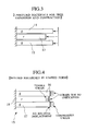
- FIG. 3 is a diagram illustrating that the glass sheets and the plastics sheet undergo free expansion and contraction in response to a temperature change
- FIG. 4 is a diagram illustrating that the glass sheets and plastics sheet bonded together are subject to strain which occurs in response to a temperature change ⁇ T;
- FIG. 5 is a diagram illustrating how strain occurs due to flexural deformation with respect to the neutral axis of the entire laminate
- FIG. 6 is a diagram illustrating a ball drop test applied to the display device substrate in the embodiment of the present invention.
- FIG. 7 is a table showing the results of the ball drop test applied to the display device substrate in the embodiment of the present invention.
- FIG. 8 is a graph showing the viscoelastic properties of the inorganic-organic hybrid material (used for the display device substrate in the embodiment of the present invention) and the epoxy resin for comparison;
- FIG. 9 is a diagram illustrating the method for press-forming the display device substrate in the first embodiment of the present invention.
- FIG. 2 is a sectional view showing the structure of a display device substrate according to a first embodiment of the present invention.
- the display device substrate 1 shown in FIG. 2 consists of a pair of glass sheets 2 and 3 facing each other and a layer 4 of plastics material held between the glass sheets 2 and 3 . It is constructed such that the glass sheets 2 and 3 have an internal compressive strain. The internal compressive strain in the glass sheets 2 and 3 is imparted by the layer 4 of plastics material held between the glass sheets 2 and 3 .
- a glass sheet is broken by an impact which produces an internal strain large enough to cause cracking.
- Glass breakage results from stress by tensile strain more readily than stress by compressive strain. In other words, breakage by impact is ascribed mainly to tensile strain.
- FIG. 3 illustrates how a glass sheet undergoes free expansion and contraction along with temperature change.
- FIG. 3 shows a pair of glass sheets 11 and 12 with a plastics sheet 13 held between them.
- each layer freely expands or contracts as the temperature changes.
- a plastics sheet contracts more than a glass sheet because the former has a larger coefficient of linear expansion than the latter.
- Contraction due to temperature change ( ⁇ T) from high to low causes a strain ( ⁇ ) which is represented by the mathematic expression (18).
- the temperature change ( ⁇ T) occurs within a range between the glass transition point (Tg) and the temperature at which the product is used or evaluated. This is because, beyond the glass transition point, the coefficient of linear expansion becomes three to four times as large as that at a normal temperature, whereas the longitudinal modulus of elasticity decreases below 1/100. In other words, stress due to strain resulting from a temperature change above Tg is too small to cause any problem.
- ⁇ T is the difference between the upper limit (the maximum temperature to be reached by the plastics material during its curing or molding or by the substrate during its production) and the product temperature.
- FIG. 4 shows an integral laminate 15 consisting of glass sheets 16 and 17 and a plastics sheet 18 , which are bonded together. Accordingly, as the temperature decreases, the plastics sheet 18 contracts more than the glass sheets 16 and 17 . As a result, a compressive strain induced by the plastics sheet 18 occurs in the glass sheets 16 and 17 , and a tensile strain induced by the glass sheets 16 and 17 occurs in the plastics sheet 18 .
- the strain ( ⁇ g) in the glass sheets 16 and 17 and the strain ( ⁇ r) in the plastics sheet 18 are related to the tensile rigidity of each material, as represented by the mathematical expression (19).
- ⁇ g ⁇ ( ⁇ g ⁇ r ) ⁇ T ⁇ ( Er ⁇ hr ) ⁇ / ⁇ ( Er ⁇ hr )+( Eg ⁇ hg ) ⁇ (20)
- ⁇ r ⁇ ( ⁇ g ⁇ r ) ⁇ T ⁇ ( Eg ⁇ hg ) ⁇ / ⁇ ( Er ⁇ hr )+( Eg ⁇ hg ) ⁇ (21)
- the glass sheets 16 and 17 and the plastics sheet 18 experience the stress ( ⁇ g) and the stress ( ⁇ r), respectively, which are represented by the following mathematical expressions (22) and (23).
- the laminate under flexure with respect to the neutral axis experiences a strain, as shown in FIG. 5 . It is assumed that the laminate 15 is bent with a radius of curvature of R. The bending moment is indicated by the arrow 20 .
- a stress ⁇ H represented by the following mathematical expression occurs at a position (H) located away from the neutral axis 19 of the laminate 15 .
- Glass in the laminate 15 breaks under the condition defined by the mathematical expression (26) if it has an internal compressive stress (g induced by the plastics material bonded thereto.
- the glass sheet 17 in the laminate 15 becomes less liable to break in proportion to the internal compressive stress ⁇ g present therein.
- ⁇ b is a value common to all glass materials and is independent of the shape (particularly thickness) of the glass materials.
- a thin glass sheet has a high resistance to flexure, but is liable to break. This is because glass becomes more flexible in inverse proportion to the third power of its thickness, but a thin glass sheet is broken by impact because impact produces a large local deformation exceeding the flexibility.
- the glass sheet (usually 0.7 mm thick) used as the display device substrate is required to be as thin as possible from the standpoint of weight reduction. Thickness reduction is also necessary to reduce the parallax which is inevitable in a display device of the reflection type composed of a pair of substrates and a liquid crystal or an organic EL material held between them and a reflector placed behind one of the substrates.
- a display device of the reflection type is made with glass sheets thinner than 0.3 mm in place of the conventional 0.7 mm thick ones, it is possible to appreciably reduce parallax to a permissible level.
- the problem with parallax is substantially solved if the display device substrate is thinner than 0.2 mm.
- the display device substrate is thinner than 0.3 mm (preferably thinner than 0.2 mm)
- a display device substrate meeting the foregoing requirements needs to be as light and strong as a 0.3 mm thick glass sheet.
- the thickness 0.3 mm is regarded as the minimum thickness that can be achieved so far.
- the effect of compressive strain should be larger than the effect of easy bending produced by replacing high-modulus glass by low-modulus plastics material.
- the display device substrate consisting of a pair of glass sheets and a plastic sheet held between them is improved in impact resistance if the constituent materials are selected such that a large compressive strain is imparted to the paired glass sheets holding a plastics sheet between them.
- the light weight and small thickness required of the display device substrate will be realized simultaneously only by employing an extremely thin glass sheet and imparting an optimum internal compressive strain to the glass sheet.
- An extremely thin glass sheet is desirable for thickness reduction but is liable to break.
- An internal compressive strain is necessary for the glass sheet to have sufficient impact resistance.
- the thickness of the display device substrate the thickness of the glass sheet, the thickness of the plastics sheet, and the characteristic properties (such as Tg, coefficient of linear expansion, and modulus of elasticity) of the plastics material.
- Each display device substrate consisted of a pair of glass sheets facing each other and a plastics sheet held between them.
- the samples varied in the total thickness of the substrate, the thickness of the glass sheet, and the thickness of the plastics sheet.
- Evaluation of the samples revealed the conditions (such as the total thickness, the thickness of glass sheet, and the thickness of plastics sheet) necessary for the display device substrate to meet requirements for light weight and small thickness, as well as better impact resistance, than the conventional 0.3 mm thick or 0.5 mm thick glass sheet.
- the samples were also used to examine how large the internal compressive strain (stress) should be in the glass sheet if the display device substrate of the laminate type is to meet the requirements for light weight and small thickness, as well as good impact resistance.
- the plastic sheet held between the paired glass sheets was formed from an inorganic-organic hybrid material based on an epoxy resin. Details of its method of manufacture and condition are given in the section of examples mentioned later.
- the inorganic-organic hybrid material based on an epoxy resin is a hard thermosetting material, as will be explained later.
- the hybrid material In its uncured state, the hybrid material is molded and then set between a pair of glass sheets. On cooling, it imparts a large stress to the glass sheets on account of its high modulus and its large coefficient of linear expansion.
- the hybrid material Being a thermosetting material, the hybrid material continues to impart an internal stress even though it is heated again after curing. Therefore, the display device substrate retains its high impact resistance.
- the plastics sheet held between the paired glass sheets should preferably be formed from a thermosetting material.
- polyurethane should be excluded, although it is thermosetting, because it is too soft to impart compressive stress.
- the samples of display device substrates were examined for impact resistance using the ball drop test shown in FIG. 6 .
- the ball drop test consists of dropping a metal ball 22 onto a sample substrate 21 that is kept in a standstill condition and observing whether cracking occurs in the sample. Details of the test, including the method for preparing the substrate, will be given later in the section of examples.
- the results of the ball drop test performed on the display device substrate in the embodiment of the present invention are tabulated in FIG. 7 .
- the results of tests on the reference samples which are formed from a glass sheet alone are also shown.
- the total thickness of the substrate is twice the thickness of the glass sheet plus the thickness of the plastics sheet.
- the thickness of the plastics sheet is obtained by subtracting the total thickness of the glass sheets from the total thickness of the substrate.
- the glass sheets whose thickness is 0.2 mm thick or less are poor in impact resistance or the substrates formed from them are broken by the metal ball falling from a height of 10 cm.
- the glass sheet which is 0.3 mm thick withstands the metal ball falling from a height of 10 cm, but it is broken by the metal ball falling from a height of 15 cm.
- the glass sheet which is 0.5 mm thick is not broken, but is scratched, by the metal ball falling from a height of 20 cm, and it is broken by the metal ball falling from a height of 25 cm.
- the display device substrate 1 (shown in FIG. 2) is composed of two glass sheets 2 and 3 (each 100 ⁇ m thick) and one layer 4 of hybrid material (100 ⁇ m thick), with the total thickness being 300 ⁇ m.
- This display device substrate proved to be comparable in impact resistance to the one formed from a single glass sheet 0.3 mm thick.
- the display device substrate which is composed of thin glass sheets according to the present invention, is comparable in impact resistance to the one formed from a thicker glass sheet owing to the thermosetting hybrid material (100 ⁇ m thick) which imparts an internal stress to the two glass sheets (200 ⁇ m thick).
- the impact resistance of the display device substrate according to the present invention is more affected by stress imparted to the glass sheets by the hybrid material than by reduction in the thickness of the high-modulus glass sheet.
- thermosetting hybrid material which is about 100 ⁇ m thick.
- the resulting display device substrate is comparable or superior in impact resistance to the one formed from a 0.3 mm thick single glass sheet.
- the display device substrate according to the present invention is constructed such that the total thickness of the glass sheets is 200 ⁇ m or less and the thickness of the layer of hybrid material is 100 ⁇ m or above, with the total thickness of the substrate being 0.3 mm or more, it is superior in impact resistance to the one formed from a 0.3 mm thick single glass sheet.
- the magnitude of the internal stress which is imparted to the glass sheets (200 ⁇ m thick) by the thermosetting hybrid material (100 ⁇ m thick) is calculated from the mathematical expressions (20) and (22).
- the mathematical expression 20 permits one to calculate the strain ⁇ g which occurs in the glass sheet (200 ⁇ m thick) due to the thermosetting hybrid material (100 ⁇ m thick).
- Thickness of hybrid material 100 ⁇ m
- ⁇ g is calculated as follows.
- the display device substrate according to the present invention will have as good an impact resistance as the one formed from a 0.3 mm thick single glass sheet, if it is formed such that a compressive strain no smaller than 1.9 ⁇ 10 ⁇ 4 is imparted to a glass sheets no thicker than 200 ⁇ m, by selecting an adequate material and adequate thickness.
- the glass sheets experience a compressive stress ( ⁇ g) which is calculated from the mathematical expression (22) as follows.
- the internal compressive strain produces the effect of partly alleviating the tensile strain (stress) due to deformation, which is induced when the glass sheet receives an impact. Therefore, the substrate with an internal compressive strain is more resistant to deformation and impact than the one without an internal compressive strain.
- each glass sheet should be no thinner than 25 ⁇ m.
- the thickness of the glass sheet should be five times at the highest compared to the thickness of the plastics sheet. (hr/hg ⁇ 5)
- the mathematical expression (20) may be simplified, as shown in the mathematical expression (29), when it is applied to the display device substrate of laminate type according to the present invention.
- the mathematical expression (2) should be satisfied so that the display device substrate is comparable or superior in impact resistance to a substrate formed from a 0.3 mm thick single glass sheet, if it has a total thickness no larger than 0.3 mm and the total thickness of the glass sheets is no larger than 200 ⁇ m.
- the glass sheets should have sufficient stiffness and crack resistance for their easy handling in the manufacturing process.
- the glass sheet meeting such requirements should preferably have a thickness of 30 ⁇ m or above, with the total thickness of the glass sheets being 60 ⁇ m or above.
- the glass sheet for easy handling should preferably have a thickness of 50 ⁇ m or above, with the total thickness of the glass sheets being 100 ⁇ m or above.
- the glass sheet should preferably have a thickness of 70 ⁇ m or above, with the total thickness of the glass sheets being 140 ⁇ m or above.
- a review of the mathematical expression (2) indicates that the mathematical expression (3) should be satisfied so that the thickness of the glass sheet is 200 ⁇ m or less and the compressive strain in the glass sheet is 1.9 ⁇ 10 ⁇ 4 or above.
- T is not the heating temperature in production, but is the difference between the Tg of the plastics material and the temperature at which the display device substrate is evaluated or used. Therefore, the important parameter of the plastics material is the difference between Tg and 20° C. (which is the average operating temperature), which is expressed by (Tg ⁇ 20)° C. And, the mathematical expression (3) should be satisfied.
- the mathematical expressions (3) and (30) may be rewritten as the mathematical expressions (4) and (31), respectively, if it is assumed that the plastics material has a modulus of elasticity higher than 1 GPa, more practically, higher than 2 GPa.
- a review of the mathematical expression (2) indicates that the mathematical expression (5) should be satisfied so that the thickness of the glass sheet is 150 ⁇ m or less for sufficient weight reduction and the compressive strain in the glass sheet is 1.9 ⁇ 10 ⁇ 4 or above for sufficient impact resistance.
- the following discussion concerns the structure of a display device substrate which is comparable or superior in impact resistance to a substrate formed from a 0.5 mm thick single glass sheet in the case where the total thickness of the substrate is 0.3 mm or less.
- the display device substrate is comparable in impact resistance to the one formed from a 0.5 mm thick single glass sheet, if it is composed of a pair of glass sheets whose total thickness is 100 ⁇ m and a plastics sheet of thermosetting hybrid material, whose thickness is 90 ⁇ m, held between them.
- the display device substrate is constructed such that the total thickness of the glass sheets is 140 ⁇ m and the thickness of the layer of thermosetting hybrid material is 140 ⁇ m, it is superior in impact resistance to one formed from a 0.5 mm thick single glass sheet and it is also superior in impact resistance to one which is composed of a pair of glass sheets (each 50 ⁇ m thick) and a layer of thermosetting hybrid material (90 ⁇ m thick) held between them.
- the stress in the glass sheets is calculated from the mathematical expressions (20) and (22) if the display device substrate has a total thickness of 100 ⁇ m and the layer of thermosetting hybrid material has a thickness of 90 ⁇ m.
- strain ( ⁇ g) that is induced in the glass sheets is calculated as follows from the mathematical expression (20).
- the glass sheets should have sufficient stiffness and crack resistance to provide for easy handling in the manufacturing process.
- a glass sheet meeting such requirements should preferably have a thickness of 30 ⁇ m or above, with the total thickness of glass sheets being 60 ⁇ m or above.
- the glass sheet for easy handling should preferably have a thickness of 50 ⁇ m or above, with the total thickness of glass sheets being 100 ⁇ m or above.
- the glass sheet should preferably have a thickness of 70 ⁇ m or above, with the total thickness of glass sheets being 140 ⁇ m or above.
- a review of the mathematical expression (8) indicates that the mathematical expression (9) should be satisfied so that the thickness of the glass sheet is 140 ⁇ m or less for sufficient weight reduction and the compressive strain in the glass sheet is 3.4 ⁇ 10 ⁇ 4 or above for sufficient impact resistance.
- ⁇ T is the difference between the Tg of the plastics material and the temperature at which the display device substrate is evaluated or used. Therefore, the important parameter of the plastics material is the value expressed by (Tg ⁇ 20)° C. And, the mathematical expression (34) should be satisfied.
- the mathematical expressions (9) and (34) may be rewritten as the mathematical expressions (10) and (35), respectively, if it is assumed that the plastics material has a modulus of elasticity higher than 1 GPa, more practically, higher than 2 GPa.
- a review of the mathematical expression (8) indicates that the mathematical expression (11) should be satisfied so that the thickness of the glass sheet is 100 ⁇ m or less for sufficient weight reduction and the compressive strain in the glass sheet is 3.7 ⁇ 10 ⁇ 4 or above.
- ⁇ T is the difference between the Tg of the plastics material and the temperature at which the display device substrate is evaluated or used. Therefore, the important parameter of the plastics material is the value expressed by (Tg ⁇ 20)° C. And, the mathematical expression (45) should be satisfied.
- the mathematical expressions (11) and (36) may be rewritten as the mathematical expressions (12) and (37), respectively, if it is assumed that the plastics material has a modulus of elasticity higher than 1 GPa, more practically, higher than 2 GPa.
- the glass sheets should have sufficient stiffness and crack resistance for their easy handling in the manufacturing process.
- the glass sheet meeting such requirements should preferably have a thickness of 30 ⁇ m or above, with the total thickness of the glass sheets being 60 ⁇ m or above.
- the glass sheet for easy handling should preferably have a thickness of 50 ⁇ m or above, with the total thickness of glass sheets being 100 ⁇ m or above.
- the glass sheet should preferably have a thickness of 70 ⁇ m or above, with the total thickness of glass sheets being 140 ⁇ m or above.
- ⁇ T is the difference between the Tg of the plastics material and the temperature at which the display device substrate is evaluated or used. Therefore, the important parameter of the plastics material is the value expressed by (Tg ⁇ 20)° C. And, the mathematical expression (38) should be satisfied.
- the mathematical expressions (15) and (38) may be rewritten as the mathematical expressions (16) and (39), respectively, if it is assumed that the plastics material has a modulus of elasticity higher than 1 GPa, more practically, higher than 2 GPa.
- the following discussion is about the structure of the display device substrate which is comparable or superior in impact resistance to a substrate formed from a 0.5 mm thick single glass sheet in the case where the total thickness of the substrate is 0.3 mm or less.
- the display device substrate is comparable in impact resistance to the one formed from a 0.5 mm thick single glass sheet, if it is composed of a pair of glass sheets whose total thickness is 140 ⁇ m and a plastics sheet of thermosetting hybrid material whose thickness is 140 ⁇ m held between them.
- the stress in the glass sheets is calculated from the mathematical expressions (20) and (22), if the display device substrate has a total thickness of 140 ⁇ m and the layer of thermosetting hybrid material has a thickness of 140 ⁇ m.
- the compressive strain ( ⁇ g) that is induced in the glass sheets is calculated as follows from the mathematical expression (20).
- the glass sheets should have sufficient stiffness and crack resistance for their easy handling in the manufacturing process.
- the glass sheet meeting such requirements should preferably have a thickness of 50 ⁇ m or above, with the total thickness of glass sheets being 100 ⁇ m or above.
- the glass sheet for easy handling should preferably have a thickness of 50 ⁇ m or above, with the total thickness of glass sheets being 100 ⁇ m or above.
- the glass sheet should preferably have a thickness of 70 ⁇ m or above, with the total thickness of glass sheets being 140 ⁇ m or above.
- the display device substrate according to the present invention has a plastics sheet held between a pair of glass sheets. This plastic sheet will be explained in the following.
- the plastics sheet held between a pair of glass sheets should be formed from a material which can give the glass sheets a sufficient compressive strain for the substrate to have a desired impact resistance. Any plastics material can be used so long as it meets the above-mentioned requirements.
- the plastics sheet held between the paired glass sheets should preferably be formed from a thermosetting material so that the display device substrate has a good impact resistance.
- polyurethane should be excluded although it is thermosetting, because it is too soft to impart compressive stress.
- An uncolored epoxy resin is desirable because it permits the display device substrate to have a high light transmission.
- a desirable plastics material is one which has a high glass transition point (Tg) so that it imparts a large compressive stress to the glass sheets.
- Tg glass transition point
- ⁇ T temperature difference
- An effective way of increasing the Tg of the plastics material is by incorporation with an inorganic material. It is desirable to use an inorganic-organic hybrid material which has both the advantage of an organic material and the advantage of an inorganic material (good mechanical properties at high temperatures and good heat resistance).
- the upper limit of the range of temperature variation is usually determined by the Tg.
- An example of the inorganic-organic hybrid material that can be used is one which is synthesized from a thermosetting resin and an organosilicon compound, the former being produced by a new process of addition polymerization disclosed in Japanese Patent Laid-open No. 2000-109709.
- the hybrid material Being based on a hard epoxy resin, the hybrid material is hard and has a high Tg. Its additional advantage is that, when a temperature exceeding Tg is applied at the time of substrate production, the upper limit of the range of temperature variation ( ⁇ T) is not Tg, but the temperature applied.
- FIG. 8 is a graph showing the viscoelastic properties of the inorganic-organic hybrid material (used for the display device substrate in the embodiment of the present invention) and the epoxy resin for comparison.
- inorganic-organic hybrid material decreases in elastic modulus much less than an epoxy resin and other plastics materials even at a temperature above the Tg, as shown in FIG. 8 .
- ⁇ T range of temperature variation
- the compressive stress imparted to the glass sheets is proportional to the temperature which is applied to the hybrid material during the manufacturing process. Therefore, it is possible to produce a very large compressive stress, as desired.
- the inorganic-organic hybrid material used for the display device substrate of the present invention should preferably be one which is synthesized from a thermosetting resin of the addition polymerization type and an organosilicon compound.
- a thermosetting resin of the addition polymerization type and an organosilicon compound One based on an epoxy resin and silicone is desirable because of its high transmission and its good film-forming ability.
- the inorganic-organic hybrid material that can be used for the display device substrate of the present invention has a molecular structure as will be explained in the following.
- the inorganic-organic hybrid material should preferably be formed from a compound represented by the chemical formula (3) or (4) and a thermosetting resin of the addition polymerization type. Before use, it is incorporated with a hardener for the thermosetting resin. It has a low viscosity before it is cured, and hence it can be readily molded to have a desired shape, thereby facilitating the production of the display device substrate.
- R denotes an organic group having a functional group capable of reaction with the hardener for the thermosetting resin
- R 1 to R 6 each denote a silicon-containing group having 0 to 3 repeating units represented by (SiOR 3/2 ).
- sol-gel process One way to produce the inorganic-organic hybrid material is by a sol-gel process. This process permits fine powder on the order of micrometer or less of a metal oxide or an organometal oxide to be formed in the matrix of high polymer at a temperature low enough (say, 100-150° C.) for the organic compound to remain intact. Therefore, hybridization can be accomplished by using the sol-gel process, which permits an epoxy resin to be used as a matrix of organic polymer.
- the sol-gel process for hybridization with an epoxy resin and an epoxy-type organosilicon alkoxide involves the reactions represented by the chemical equations (5) and (6).
- the reactions represented by the chemical equations (5) and (6) are carried out in n epoxy resin.
- a hardener for the epoxy resin is added.
- the hardener include amine compounds, quaternary ammonium salts, dicyandiamide, carboxylic acid anhydride, boron trifluoride-amine complex, hydrazide of organic acid, imidazole compounds, phenol, cresol, xylenol, and phenolic resin. Addition reactions take place among epoxy groups in the organosilicon compound, epoxy groups in the epoxy resin, and amino groups in the hardener.
- reaction eventually gives rise to an inorganic-organic hybrid material of epoxy-silicon type which contains a uniformly dispersed organosilicon compound forming covalent bonding with the hardener.
- This hybrid material can be used to manufacture the display device substrate.
- An open system may be employed for the reactions represented by the chemical equations (5) and (6) to be performed in an epoxy resin.
- the reactions may be carried out under a nitrogen stream by using a reaction vessel equipped with a distillatory apparatus which removes at least part of the evolved alcohol and water from the system.
- reaction product or the inorganic-organic hybrid material is immune from discoloration.
- the reaction product free of discoloration contributes to the display device substrate having a high transmission.
- reaction product which is a hydrolyzate of an organosilicon alkoxide is thermally stable.
- the result is a long pot life for the mixture of the epoxy resin and the hydrolyzate of organosilicon alkoxide. This means that the reaction can be performed to give a large amount of product which is used later little by little for production of the display device substrate.
- the reaction may also be carried out under a nitrogen stream by using a reaction vessel equipped with a reflux condenser in such a way that the revolved alcohol and water are returned to the reaction vessel during reaction.
- reaction with refluxing promotes the sol-gel process, thereby reducing the reaction time and substrate manufacturing time.
- Reactions under a nitrogen stream prevents the reaction product or the inorganic-organic hybrid material from discoloration.
- the reaction product free of discoloration contributes to the display device substrate having a high transmission.
- the reactions represented by the chemical equations (5) and (6) may also be carried out in the following way. First, they are previously carried out independently so as to give an oligomer of the organosilicon alkoxide. Then, the resulting oligomer is mixed with an epoxy resin. The mixture is incorporated with a hardener for reaction to yield the inorganic-organic hybrid material of epoxy-silicon type.
- Oligomerization preceding the reaction with an epoxy resin prevents side reactions which would otherwise take place in the sol-gel process. This prevents discoloration of the epoxy resin and, hence, gives rise to a clear hybrid material.
- the epoxy resin suitable for the hybrid material includes that of the glycidyl ether type composed mainly of a phenolic compound such as bisphenol-A, bisphenol-F, tetrabromobisphenol-A, tetraphenylolethane, phenol-novolak, and o-cresol-novolak; that of the glycidyl ether type composed mainly of an alcoholic compound such as polypropylene glycol and hydrogenated bisphenol-A; that of the glycidyl ester type composed mainly of hexahydrophthalic anhydride or dimmer acid; that of the glycidyl amine type composed mainly of diaminophenylmethane, isocyanuric acid, or hydantoin; that of the mixed type composed mainly of p-aminophenol or p-oxybenzoic acid; that composed mainly of an ester represented by the chemical formula (2) below; and a mixture thereof.
- a phenolic compound
- the hybrid material used for production of the display device substrate should contain a prescribed amount of silicon.
- the silicon content is expressed in terms of SiO 2 . It is calculated by dividing the amount of silicon in terms of SiO 2 in the organosilicon compound by the total amount of epoxy resin, hardener, and hydrolyzed organosilicon alkoxide.
- the silicon content (in terms of SiO 2 ) in the hybrid material should be more than 0 wt % and less than 30 wt %, so that the hybrid material has a good heat resistance characteristic of inorganic materials.
- the hybrid material With a silicon content (in terms of SiO 2 ) more than 30 wt %, the hybrid material has difficulties in uniform dispersion of the compound represented by the chemical formulas (3) or (4). It leads to a display device substrate that is poor in impact resistance.
- the silicon content (in terms of SiO 2 ) should preferably be no less than 4 wt % and no more than 15 wt %.
- the hybrid material With a silicon content (in terms of SiO 2 ) no less than 4 wt %, the hybrid material produces a marked effect due to inorganic-organic hybridization and contributes to a display device substrate that is superior in heat resistance. With a silicon content no more than 15 wt %, the hybrid material permits uniform dispersion of the compound represented by the chemical formulas (3) or (4) and contributes to display device substrate that is superior in impact resistance.
- the display device substrate according to the present invention is composed of a pair of glass sheets and a layer of plastics materials held between them, so that it is light in weight and small in thickness and yet it is highly reliable with good a impact resistance.
- the first step is to prepare a varnish as a starting material for the layer of the inorganic-organic hybrid material composed of an epoxy resin and an organosilicon compound.
- the following reactants are placed in a reaction vessel so that the silicon content (in terms of SiO 2 ) therein is 8 wt %.
- the reactants are mixed and allowed to stand overnight at room temperature.
- the reaction vessel is given 30 g of an epoxy resin represented by the chemical formula (8).
- the reactants are stirred at room temperature for 30 minutes.
- the reaction vessel is provided with a distillatory apparatus.
- the reactants are heated at 150° C. with stirring for 4 hours. Reaction is carried out under a nitrogen stream, and methanol and water are removed from the reaction liquid by distillation.
- reaction liquid After cooling to room temperature, the reaction liquid is given 16.5 g of phenolic resin as a hardener for the epoxy resin represented by the chemical formula (10) and 0.3 g of triphenylphosphine as a cure accelerator. The reactants are heated at 80° C. for 2 minutes.
- FIG. 9 is a diagram illustrating the method press-forming the display device substrate in accordance with the first embodiment of the present invention.
- the display device substrate in this example is formed by press molding as shown in FIG. 9 .
- the varnish 31 which has been prepared as mentioned above, is cast onto a glass sheet 3 measuring 30 mm by 70 mm and 70 ⁇ m thick. This glass sheet is previously heated at 120° C. and placed on a polyimide sheet 32 .
- the thus obtained laminate is held between a pair of stainless steel mirror plates 35 and 36 (2 mm thick).
- the entire assembly is held between layers of amide fiber 37 and 38 (3.8 mm thick).
- press molding is performed to produce the press molding assembly 30 .
- the press molding assembly is pressed at 120° C. for 15 minutes and then at 160° C. for 120 minutes.
- the display device substrate shown in FIG. 2 which is composed of a pair of glass sheets 2 and 3 and a layer 4 (140 ⁇ m thick) of the inorganic-organic hybrid material of epoxy-silicon type held between the glass sheets.
- the thus obtained display device substrate 1 has an internal compressive strain in the glass sheets 2 and 3 .
- the internal compressive strain in the glass sheets 2 and 3 is imparted by the layer 4 of the inorganic-organic hybrid material of epoxy-silicon type held between the glass sheets.
- the above-mentioned inorganic-organic hybrid material of epoxy-silicone type used in this example has the following physical properties.
- Thickness of hybrid material 140 ⁇ m
- the glass sheets used in this example have the following physical properties.
- the value of ⁇ ( ⁇ r ⁇ T ⁇ (Er ⁇ hr) ⁇ /(Eg ⁇ hg) according to the mathematical expression (26) is 4 ⁇ 10 ⁇ 4 .
- the value of ⁇ r ⁇ T ⁇ (Er ⁇ hr) ⁇ is 4100 Pa ⁇ m and the value of ⁇ r ⁇ T ⁇ hr ⁇ is 3.0 ⁇ 10 ⁇ 6 .
- the relation defined by the mathematical expressions 3 and 4 are satisfied.
- the display device substrate 1 obtained in this example was measured for light transmission. It was found that the transmission of light with a wavelength of 400 nm and 540 nm was 93% and 97%, respectively.
- the present invention can provide a display device substrate having a very high transmission.
- the display device substrate 1 obtained in this example was measured for weight.
- the sample measures 10 mm by 10 mm in size.
- the weight was compared with that of a 0.3 mm thick glass sheet.
- the display device substrate 1 in this example is as light as 0.0455 g, whereas the glass sheet for comparison weighs 0.0713 g. In other words, the former is lighter than the latter by about 40% even though they have the same thickness.
- the present invention can provide a light display device substrate.
- the display device substrate obtained in Example 1 was tested for heat resistance.
- the sample was allowed to stand in an oven at 150° C. for 1 hour, and then it was visually examined for discoloration. No discoloration was noticed.
- the display device substrate 1 in this example has a good heat resistance.
- the present invention can provide a light display device substrate with good heat resistance.
- the layer of the inorganic-organic hybrid material of epoxy-silicone type was examined for viscoelastic properties in the following manner.
- the hybrid material was held between two polyimide sheets without using glass sheets and the assembly was pressed for curing.
- a sample for comparison was prepared from an epoxy resin represented by the chemical formula (8), a phenolic resin represented by the chemical formula (10) as a hardener for the epoxy resin, and triphenylphosphine as a cure accelerator, without using GTMS, purified water, and di-n-butyltin dilaurate.
- the sample was press-formed under the same conditions as mentioned above. Thus, there was obtained an unhybridized sample of the epoxy resin.
- the sample of the epoxy resin for comparison decreases in viscoelasticity steeply in the neighborhood of 145° C. or the glass transition point (Tg), whereas the sample of the hybrid material decreases in viscoelasticity only slightly in the neighborhood of 145° C.
- the sample in this example is higher in viscoelasticity at Tg and above that value by more than one order of magnitude.
- This example is intended to determine how the impact resistance is related with the total thickness of the display device substrate, the thickness of the glass sheet, and the thickness of the plastics layer.
- the example is also intended to find the optimal condition for the display device substrate to have an impact resistance better than that of a 0.3 mm or 0.5 mm thick glass sheet despite its light weight and small thickness.
- several kinds of display device substrates were prepared, which differ in the total thickness of the display device substrate, the thickness of the glass sheet, and the thickness of the plastics layer.
- Other samples differing in the thickness of the spacer used in pressing, and hence differing in the thickness of hybrid material, were prepared under the same condition as in Example 1.
- Glass/HB/glass 70/140/70, 50/90/50, 100/100/100, and 200/420/200.
- the test method for evaluation is schematically shown in FIG. 6 . It consists of dropping a steel ball 22 (12.7 mm in diameter and 8.343 g in weight) onto the center of the sample 21 (measuring 30 mm by 70 mm) placed on a wood stand. The impact resistance of the sample is rated by whether or not cracking occurs in the sample.
- the table in FIG. 7 shows the results of tests on the display device substrates according to the present invention and the glass substrate for comparison.
- the display device substrate according to the present invention is superior in impact resistance.
- the present invention can provide a display device substrate with good impact resistance.
- the display device substrate obtained in Example 1 underwent known sputtering at 200° C. to form on one side thereof a 100 nm thick layer of ITO (indium-tin oxide) as a transparent conducting material.
- ITO indium-tin oxide
- the resulting substrate with an ITO electrode is flat and highly transparent.
- the ITO layer was etched to form electrodes in a stripe pattern. Each electrode is 6 mm wide and spaced 0.5 mm from adjacent ones.
- That side of the substrate on which electrodes are formed was coated by spin coating with a varnish (with 2% solids) of polyamic acid as a precursor of polyamide.
- the coated substrate was dried at 80° C. for solvent removal and then baked at 200° C. for 15 minutes. In this way there was formed a polyimide alignment film (100 nm thick) on the electrodes.
- the polyimide alignment film underwent rubbing by using a rubbing machine (from Fujioka) equipped with a rubbing roll (100 mm in diameter) wrapped with a rayon cloth. Rubbing was carried out under the following conditions.
- Substrate feed rate 30 mm/second
- Pushing depth 0.4 mm
- a sealing material thermosetting resin
- a spacer was scattered onto the alignment film of the other substrate with electrodes.
- the two substrates were bonded together, with the alignment films facing each other, in such a way that the rubbing directions (or the liquid crystal aligning directions) on the alignment film were perpendicular to each other, and that the two substrates were slightly dislocated a few millimeters from each other to facilitate wiring to the electrodes to which a voltage is applied from outside.
- the two substrates were pressed at 150° C. for 2 hours, so that they were firmly bonded together. Thus, there was obtained an LCD panel.
- the gap between the two substrates was 5 ⁇ m.
- the thus obtained LCD panel was filled with a liquid crystal material through an opening in the seal.
- the opening was closed with a UV-curable resin.
- liquid crystal display device of the TN mode which has normally open characteristics (in which a white display appears when the applied voltage is low and a black display appears when the applied voltage is high).
- a voltage (4V) was applied to the LCD panel through the exposed electrodes of the two substrates.
- the voltage application caused the liquid crystal to change in orientation.
- the white display region without voltage application turned to black.
- Example 1 This example proved that the display device substrate obtained in Example 1 can be made into a liquid crystal display device via the process of LCD panel fabrication.
- the display device substrate obtained in Example 1 is adaptable to the conventional LCD manufacturing process on account of ITO electrodes formed thereon, and that it can be used to form a liquid crystal display device.
- the display device substrate according to the present invention meets requirements for weight reduction, thickness reduction, high reliability (good gas barrier properties), good heat resistance, and good impact resistance.
- the present invention provides a display device substrate of laminate structure composed of glass sheets and a plastics sheet, which is comparable or superior in impact resistance to a substrate formed with a 0.3 mm thick glass sheet alone, because the plastics sheet protects the glass sheets from cracking.
- the present invention provides a liquid crystal display device or an organic EL device, which is light in weight and small in thickness and is superior in impact resistance and display quality, by utilizing a conventional material and manufacturing process.
- the present invention provides a display device substrate which is light in weight and small in thickness and superior in impact resistance.
Landscapes
- Physics & Mathematics (AREA)
- Nonlinear Science (AREA)
- Mathematical Physics (AREA)
- Chemical & Material Sciences (AREA)
- Crystallography & Structural Chemistry (AREA)
- General Physics & Mathematics (AREA)
- Optics & Photonics (AREA)
- Devices For Indicating Variable Information By Combining Individual Elements (AREA)
- Liquid Crystal (AREA)
- Laminated Bodies (AREA)
- Electroluminescent Light Sources (AREA)
- Surface Treatment Of Glass (AREA)
Abstract
Description


Claims (47)


Priority Applications (1)
| Application Number | Priority Date | Filing Date | Title |
|---|---|---|---|
| US10/688,978 US20040080676A1 (en) | 2001-10-18 | 2003-10-21 | Display device substrate and display device formed therewith |
Applications Claiming Priority (2)
| Application Number | Priority Date | Filing Date | Title |
|---|---|---|---|
| JP2001320062A JP3864750B2 (en) | 2001-10-18 | 2001-10-18 | Display element substrate and display element using the same |
| JP2001-320062 | 2001-10-18 |
Related Child Applications (1)
| Application Number | Title | Priority Date | Filing Date |
|---|---|---|---|
| US10/688,978 Continuation US20040080676A1 (en) | 2001-10-18 | 2003-10-21 | Display device substrate and display device formed therewith |
Publications (2)
| Publication Number | Publication Date |
|---|---|
| US20030077453A1 US20030077453A1 (en) | 2003-04-24 |
| US6660387B2 true US6660387B2 (en) | 2003-12-09 |
Family
ID=19137505
Family Applications (2)
| Application Number | Title | Priority Date | Filing Date |
|---|---|---|---|
| US10/101,167 Expired - Lifetime US6660387B2 (en) | 2001-10-18 | 2002-03-20 | Display device substrate and display device formed therewith |
| US10/688,978 Abandoned US20040080676A1 (en) | 2001-10-18 | 2003-10-21 | Display device substrate and display device formed therewith |
Family Applications After (1)
| Application Number | Title | Priority Date | Filing Date |
|---|---|---|---|
| US10/688,978 Abandoned US20040080676A1 (en) | 2001-10-18 | 2003-10-21 | Display device substrate and display device formed therewith |
Country Status (5)
| Country | Link |
|---|---|
| US (2) | US6660387B2 (en) |
| JP (1) | JP3864750B2 (en) |
| KR (1) | KR100827086B1 (en) |
| CN (1) | CN1231795C (en) |
| TW (1) | TWI229222B (en) |
Cited By (6)
| Publication number | Priority date | Publication date | Assignee | Title |
|---|---|---|---|---|
| US20040080676A1 (en) * | 2001-10-18 | 2004-04-29 | Hitoshi Oaku | Display device substrate and display device formed therewith |
| US20060127679A1 (en) * | 2004-12-13 | 2006-06-15 | Gulati Suresh T | Glass laminate substrate having enhanced impact and static loading resistance |
| US9321677B2 (en) | 2014-01-29 | 2016-04-26 | Corning Incorporated | Bendable glass stack assemblies, articles and methods of making the same |
| US20180341132A1 (en) * | 2017-05-26 | 2018-11-29 | Japan Display Inc. | Display device |
| US10864707B2 (en) | 2012-10-05 | 2020-12-15 | Corning Incorporated | Glass/metal laminated structures and methods of manufacturing laminated structures |
| US10953633B2 (en) | 2012-08-31 | 2021-03-23 | Corning Incorporated | Strengthened thin glass-polymer laminates |
Families Citing this family (45)
| Publication number | Priority date | Publication date | Assignee | Title |
|---|---|---|---|---|
| JP3865056B2 (en) * | 2002-01-22 | 2007-01-10 | セイコーエプソン株式会社 | Manufacturing method of sealing substrate |
| WO2004073256A1 (en) * | 2003-02-12 | 2004-08-26 | Samsung Electronics Co., Ltd. | Method for managing service context for paging user equipment in a multimedia broadcast/multicast service |
| JP4546178B2 (en) * | 2003-10-23 | 2010-09-15 | 日東電工株式会社 | Optical resin sheet, liquid crystal cell substrate including the optical resin sheet, liquid crystal display device, image display device substrate, and image display device |
| JP2005297498A (en) * | 2004-04-16 | 2005-10-27 | Dainippon Printing Co Ltd | Flexible base board, and organic device using the same |
| JP5090160B2 (en) * | 2004-05-21 | 2012-12-05 | コーニンクレッカ フィリップス エレクトロニクス エヌ ヴィ | Rollable display device with load reduction |
| CN100561304C (en) * | 2004-06-25 | 2009-11-18 | 鸿富锦精密工业(深圳)有限公司 | Packaging liquid crystal is with glass substrate and liquid crystal indicator |
| JP2007212801A (en) * | 2006-02-10 | 2007-08-23 | Fujitsu Hitachi Plasma Display Ltd | Flat panel display, and display panel device with same |
| JP4936989B2 (en) * | 2006-07-11 | 2012-05-23 | 日本合成化学工業株式会社 | LAMINATE, ITS MANUFACTURING METHOD, AND USE THEREOF |
| US20080095995A1 (en) * | 2006-10-18 | 2008-04-24 | Hong Rae Cha | Filter and flat panel display device using the filter |
| US8673163B2 (en) | 2008-06-27 | 2014-03-18 | Apple Inc. | Method for fabricating thin sheets of glass |
| TWI415044B (en) | 2008-12-15 | 2013-11-11 | Ind Tech Res Inst | Substrate board, fabrication method thereof and a display therewith |
| GB0823397D0 (en) * | 2008-12-23 | 2009-01-28 | Eastman Kodak Co | Multilayer devices on flexible supports |
| CN102388003B (en) | 2009-03-02 | 2014-11-19 | 苹果公司 | Techniques for strengthening glass covers for portable electronic devices |
| JP5498202B2 (en) * | 2009-03-03 | 2014-05-21 | 富士フイルム株式会社 | Barrier laminate, gas barrier film and device using the same |
| KR101094300B1 (en) * | 2009-10-12 | 2011-12-19 | 삼성모바일디스플레이주식회사 | Organic light emitting diode lighting apparatus and method for manufacturing the same |
| US9778685B2 (en) | 2011-05-04 | 2017-10-03 | Apple Inc. | Housing for portable electronic device with reduced border region |
| JP5480303B2 (en) * | 2010-02-02 | 2014-04-23 | シャープ株式会社 | Semiconductor device and manufacturing method thereof |
| JP2011170082A (en) * | 2010-02-18 | 2011-09-01 | Stanley Electric Co Ltd | Liquid crystal display device |
| US10189743B2 (en) | 2010-08-18 | 2019-01-29 | Apple Inc. | Enhanced strengthening of glass |
| US8824140B2 (en) | 2010-09-17 | 2014-09-02 | Apple Inc. | Glass enclosure |
| CN102478727B (en) | 2010-11-28 | 2016-04-06 | 宸鸿科技(厦门)有限公司 | The manufacture method of touch control display apparatus and display device, touch control display apparatus |
| US9725359B2 (en) | 2011-03-16 | 2017-08-08 | Apple Inc. | Electronic device having selectively strengthened glass |
| US10781135B2 (en) | 2011-03-16 | 2020-09-22 | Apple Inc. | Strengthening variable thickness glass |
| US9128666B2 (en) | 2011-05-04 | 2015-09-08 | Apple Inc. | Housing for portable electronic device with reduced border region |
| KR102043666B1 (en) | 2011-05-13 | 2019-12-02 | 니폰 덴키 가라스 가부시키가이샤 | Laminate, method for cutting laminate, method for processing laminate, and device and method for cutting brittle plate-like object |
| JP6016067B2 (en) * | 2011-05-13 | 2016-10-26 | 日本電気硝子株式会社 | Laminated body |
| US9944554B2 (en) | 2011-09-15 | 2018-04-17 | Apple Inc. | Perforated mother sheet for partial edge chemical strengthening and method therefor |
| US9516149B2 (en) | 2011-09-29 | 2016-12-06 | Apple Inc. | Multi-layer transparent structures for electronic device housings |
| US10144669B2 (en) | 2011-11-21 | 2018-12-04 | Apple Inc. | Self-optimizing chemical strengthening bath for glass |
| US10133156B2 (en) | 2012-01-10 | 2018-11-20 | Apple Inc. | Fused opaque and clear glass for camera or display window |
| US8773848B2 (en) | 2012-01-25 | 2014-07-08 | Apple Inc. | Fused glass device housings |
| US9946302B2 (en) | 2012-09-19 | 2018-04-17 | Apple Inc. | Exposed glass article with inner recessed area for portable electronic device housing |
| CN105517796B (en) * | 2013-01-07 | 2018-03-30 | 康宁股份有限公司 | Strengthen laminated glass construction |
| NL2010625C2 (en) * | 2013-04-11 | 2014-10-14 | Aviat Glass & Technology B V | MIRROR, AND METHOD FOR MANUFACTURING SUCH MIRROR |
| US9459661B2 (en) | 2013-06-19 | 2016-10-04 | Apple Inc. | Camouflaged openings in electronic device housings |
| DE102013214426A1 (en) * | 2013-07-24 | 2015-01-29 | Schott Ag | Composite element and its use |
| DE102013214422A1 (en) * | 2013-07-24 | 2015-01-29 | Schott Ag | Composite element and its use |
| KR102266941B1 (en) * | 2013-12-19 | 2021-06-18 | 삼성디스플레이 주식회사 | Organic light emitting display device |
| US9886062B2 (en) | 2014-02-28 | 2018-02-06 | Apple Inc. | Exposed glass article with enhanced stiffness for portable electronic device housing |
| US10472277B2 (en) | 2014-07-28 | 2019-11-12 | Dell Products L.P. | Composite plastic display cover |
| US10737467B2 (en) | 2014-08-25 | 2020-08-11 | Dell Products L.P. | Multilayer glass composite display cover |
| KR102352284B1 (en) * | 2015-02-02 | 2022-01-18 | 삼성디스플레이 주식회사 | Rollable display device |
| KR20180051695A (en) * | 2016-11-07 | 2018-05-17 | 삼성디스플레이 주식회사 | Glass substrate, manufacturing method of the same, and display device having the same |
| WO2020112467A1 (en) * | 2018-11-30 | 2020-06-04 | Corning Incorporated | Thin multilayer laminate |
| WO2023277060A1 (en) * | 2021-06-30 | 2023-01-05 | 積水化学工業株式会社 | Laminate, electronic device, resin composition and cover glass |
Citations (2)
| Publication number | Priority date | Publication date | Assignee | Title |
|---|---|---|---|---|
| JPS57196747A (en) * | 1981-05-29 | 1982-12-02 | Bridgestone Corp | Laminated glass |
| US6172457B1 (en) * | 1997-03-25 | 2001-01-09 | Telegen Corporation | Thermally compatible ceramic collars for flat panel displays |
Family Cites Families (8)
| Publication number | Priority date | Publication date | Assignee | Title |
|---|---|---|---|---|
| JP3059866B2 (en) * | 1993-07-30 | 2000-07-04 | シャープ株式会社 | Substrate for display device |
| JP3017912B2 (en) * | 1993-12-13 | 2000-03-13 | シャープ株式会社 | Electrode substrate for liquid crystal display device and liquid crystal display device |
| JPH07287218A (en) * | 1994-04-20 | 1995-10-31 | Toshiba Corp | Transparent conductive substrate and display device using the same |
| KR100211633B1 (en) * | 1996-06-26 | 1999-08-02 | 구자홍 | A thin glass substrate having passivation layer of lcd and method for manufacturing thereof |
| JP3414205B2 (en) * | 1997-06-27 | 2003-06-09 | 日本板硝子株式会社 | Laminated glass |
| JPH11295702A (en) * | 1998-04-06 | 1999-10-29 | Sony Corp | Image display device |
| JP2000352709A (en) * | 1999-06-11 | 2000-12-19 | Dainippon Printing Co Ltd | Film substrate for liquid crystal display device |
| JP3864750B2 (en) * | 2001-10-18 | 2007-01-10 | 株式会社日立製作所 | Display element substrate and display element using the same |
-
2001
- 2001-10-18 JP JP2001320062A patent/JP3864750B2/en not_active Expired - Fee Related
-
2002
- 2002-03-20 US US10/101,167 patent/US6660387B2/en not_active Expired - Lifetime
- 2002-03-29 TW TW091106299A patent/TWI229222B/en not_active IP Right Cessation
- 2002-06-05 CN CNB021224072A patent/CN1231795C/en not_active Expired - Fee Related
- 2002-08-19 KR KR1020020048885A patent/KR100827086B1/en not_active IP Right Cessation
-
2003
- 2003-10-21 US US10/688,978 patent/US20040080676A1/en not_active Abandoned
Patent Citations (2)
| Publication number | Priority date | Publication date | Assignee | Title |
|---|---|---|---|---|
| JPS57196747A (en) * | 1981-05-29 | 1982-12-02 | Bridgestone Corp | Laminated glass |
| US6172457B1 (en) * | 1997-03-25 | 2001-01-09 | Telegen Corporation | Thermally compatible ceramic collars for flat panel displays |
Cited By (16)
| Publication number | Priority date | Publication date | Assignee | Title |
|---|---|---|---|---|
| US20040080676A1 (en) * | 2001-10-18 | 2004-04-29 | Hitoshi Oaku | Display device substrate and display device formed therewith |
| US20060127679A1 (en) * | 2004-12-13 | 2006-06-15 | Gulati Suresh T | Glass laminate substrate having enhanced impact and static loading resistance |
| US7201965B2 (en) | 2004-12-13 | 2007-04-10 | Corning Incorporated | Glass laminate substrate having enhanced impact and static loading resistance |
| US10953633B2 (en) | 2012-08-31 | 2021-03-23 | Corning Incorporated | Strengthened thin glass-polymer laminates |
| US10864707B2 (en) | 2012-10-05 | 2020-12-15 | Corning Incorporated | Glass/metal laminated structures and methods of manufacturing laminated structures |
| US9321678B2 (en) | 2014-01-29 | 2016-04-26 | Corning Incorporated | Bendable glass stack assemblies, articles and methods of making the same |
| US9557773B2 (en) | 2014-01-29 | 2017-01-31 | Corning Incorporated | Bendable glass stack assemblies, articles and methods of making the same |
| US9898046B2 (en) | 2014-01-29 | 2018-02-20 | Corning Incorporated | Bendable glass stack assemblies, articles and methods of making the same |
| US10809766B2 (en) | 2014-01-29 | 2020-10-20 | Corning Incorporated | Bendable glass stack assemblies, articles and methods of making the same |
| US10824200B2 (en) | 2014-01-29 | 2020-11-03 | Corning Incorporated | Bendable glass stack assemblies, articles and methods of making the same |
| US9321679B2 (en) | 2014-01-29 | 2016-04-26 | Corning Incorporated | Bendable glass stack assemblies, articles and methods of making the same |
| US9321677B2 (en) | 2014-01-29 | 2016-04-26 | Corning Incorporated | Bendable glass stack assemblies, articles and methods of making the same |
| US11358372B2 (en) | 2014-01-29 | 2022-06-14 | Corning Incorporated | Bendable glass stack assemblies, articles and methods of making the same |
| US11745471B2 (en) | 2014-01-29 | 2023-09-05 | Corning Incorporated | Bendable glass stack assemblies, articles and methods of making the same |
| US20180341132A1 (en) * | 2017-05-26 | 2018-11-29 | Japan Display Inc. | Display device |
| US10859869B2 (en) * | 2017-05-26 | 2020-12-08 | Japan Display Inc. | Display device |
Also Published As
| Publication number | Publication date |
|---|---|
| CN1231795C (en) | 2005-12-14 |
| KR20030032832A (en) | 2003-04-26 |
| US20040080676A1 (en) | 2004-04-29 |
| KR100827086B1 (en) | 2008-05-02 |
| JP3864750B2 (en) | 2007-01-10 |
| TWI229222B (en) | 2005-03-11 |
| JP2003122269A (en) | 2003-04-25 |
| US20030077453A1 (en) | 2003-04-24 |
| CN1412610A (en) | 2003-04-23 |
Similar Documents
| Publication | Publication Date | Title |
|---|---|---|
| US6660387B2 (en) | Display device substrate and display device formed therewith | |
| EP2223957B1 (en) | Transparent composite compound | |
| KR100347973B1 (en) | Transparent conductive sheet | |
| US8658755B2 (en) | Silicon-containing curable composition and cured product thereof | |
| US7438958B2 (en) | Sealant composition for liquid crystal and process for producing liquid-crystal display panel with the same | |
| EP1471112A1 (en) | Transparent composite composition | |
| KR101811893B1 (en) | Transparent substrate | |
| US20080161473A1 (en) | Hybrid composition and films fabricated by the same | |
| US20160082699A1 (en) | Resin layer-attached supporting substrate and method for producing same, glass laminate and method for producing same, and method for producing electronic device | |
| KR101127253B1 (en) | Transparent composite sheet, multilayer sheet and liquid crystal display element | |
| JP7539366B2 (en) | Polyamic acid composition and method for producing same, polyamic acid solution, polyimide, polyimide film, laminate and method for producing same, and flexible device and method for producing same | |
| JP2005206787A (en) | Transparent complex composition | |
| US20170298198A1 (en) | Aromatic polyamide films for solvent resistant flexible substrates | |
| US9209403B2 (en) | Method for fabricating flexible electrical devices | |
| US20180057648A1 (en) | Silicone resin transparent substrate and method for manufacturing the same | |
| JP4060116B2 (en) | Plastic substrate for display element | |
| EP1924637B1 (en) | Negative c-type compensation film and method of preparing the same | |
| JP4180450B2 (en) | Transparent composite sheet | |
| JP3818638B2 (en) | Plastic substrate for display element and method for manufacturing plastic substrate for display element | |
| JP6571946B2 (en) | Transparent substrate | |
| KR100528471B1 (en) | A plastic film for display panel having a nanocomposite gas barrier layer and manufacturing method thereof | |
| JP2003122268A (en) | Substrate for display element and method of manufacturing the same | |
| US20240166914A1 (en) | Optical film having excellent impact resistance and bending properties and display device comprising same | |
| JP2000347170A (en) | Substrate for liquid crystal display panel | |
| US20160369060A1 (en) | Composition for composite sheet, composite sheet manufactured using same, and display device comprising same |
Legal Events
| Date | Code | Title | Description |
|---|---|---|---|
| AS | Assignment |
Owner name: HITACHI, LTD., JAPAN Free format text: ASSIGNMENT OF ASSIGNORS INTEREST;ASSIGNORS:OAKU, HITOSHI;HANAWA, YASUO;AMAGI, SHIGEO;AND OTHERS;REEL/FRAME:012727/0427;SIGNING DATES FROM 20020307 TO 20020312 |
|
| STCF | Information on status: patent grant |
Free format text: PATENTED CASE |
|
| FEPP | Fee payment procedure |
Free format text: PAYOR NUMBER ASSIGNED (ORIGINAL EVENT CODE: ASPN); ENTITY STATUS OF PATENT OWNER: LARGE ENTITY |
|
| FPAY | Fee payment |
Year of fee payment: 4 |
|
| FPAY | Fee payment |
Year of fee payment: 8 |
|
| AS | Assignment |
Owner name: HITACHI DISPLAYS, LTD., JAPAN Free format text: COMPANY SPLIT PLAN TRANSFERRING ONE HUNDRED (100) PERCENT SHARE OF PATENT AND PATENT APPLICATIONS;ASSIGNOR:HITACHI, LTD.;REEL/FRAME:027362/0612 Effective date: 20021001 Owner name: PANASONIC LIQUID CRYSTAL DISPLAY CO., LTD., JAPAN Free format text: MERGER/CHANGE OF NAME;ASSIGNOR:IPS ALPHA SUPPORT CO., LTD.;REEL/FRAME:027363/0315 Effective date: 20101001 Owner name: IPS ALPHA SUPPORT CO., LTD., JAPAN Free format text: COMPANY SPLIT PLAN TRANSFERRING FIFTY (50) PERCENT SHARE OF PATENTS AND PATENT APPLICATIONS;ASSIGNOR:HITACHI DISPLAYS, LTD.;REEL/FRAME:027362/0466 Effective date: 20100630 |
|
| FPAY | Fee payment |
Year of fee payment: 12 |