US6593243B1 - Method of manufacturing semiconductor device - Google Patents
Method of manufacturing semiconductor device Download PDFInfo
- Publication number
- US6593243B1 US6593243B1 US09/632,163 US63216300A US6593243B1 US 6593243 B1 US6593243 B1 US 6593243B1 US 63216300 A US63216300 A US 63216300A US 6593243 B1 US6593243 B1 US 6593243B1
- Authority
- US
- United States
- Prior art keywords
- etching
- layer
- semiconductor device
- mask material
- manufacturing
- Prior art date
- Legal status (The legal status is an assumption and is not a legal conclusion. Google has not performed a legal analysis and makes no representation as to the accuracy of the status listed.)
- Expired - Fee Related
Links
Images


Classifications
-
- H10P14/61—
-
- H10P50/71—
-
- H10P50/283—
Definitions
- the present invention relates to methods of manufacturing semiconductor devices and, more particularly to a method of manufacturing a semiconductor device capable of forming a pattern such as an extremely fine interconnection with accuracy.
- Interconnections are increasingly becoming smaller in semiconductor devices. Thus, it is becoming difficult to form such extremely fine interconnection patterns only by means of lithography.
- a hard mask including for example a silicon oxide film is applied in place of a photoresist pattern as a mask material.
- an insulating film mask (hard mask) 104 b is formed having a prescribed dimension.
- insulating film 104 a is a silicon oxide film
- a prescribed insulating film mask 104 b is formed by isotropically etching insulating film 104 a in a hydrofluoric solution.
- insulating film mask 104 b is formed by isotropically etching insulating film 104 a .
- an extremely thin hard mask may be formed. In this case, to achieve a desired interconnection dimension, control of a thickness of insulating film 104 as the hard mask becomes extremely difficult.
- An object of the present invention is to provide a method of manufacturing a semiconductor device capable of providing a mask material with a desired dimension without any variation in thickness of the mask material and preventing a layer to be the mask material from coming off a semiconductor substrate.
- a prescribed layer is formed on a main surface of a semiconductor substrate.
- a layer, which is to be used as a mask material when patterning the prescribed layer, is formed thereon.
- a photoresist pattern is formed on the layer to be the mask material.
- the layer to be the mask material is etched to form the mask material.
- the prescribed layer is etched using the mask material as a mask to form a prescribed pattern.
- the layer to be the mask material is etched in a gas phase ambient using the photoresist pattern as the mask.
- the layer to be the mask material is etched in the gas phase ambient using the photoresist pattern as the mask.
- the mask material can be formed without causing the layer to be the mask material to come off the semiconductor substrate.
- a desired mask material can be formed without causing any variation in thickness of the mask material.
- the step of forming the mask material preferably includes: a first etching step of anisotropically etching the layer to be the mask material to expose a surface of the prescribed layer using the photoresist pattern as the mask; and a second etching step of etching a side surface of the layer to be the mask material positioned under the photoresist pattern in the gas phase ambient to form the mask material.
- the mask material having a desired dimension can be formed with accuracy without causing any decrease in thickness of the layer to be the mask material. Even when the dimension of a prescribed pattern is to be changed to comply with the change in design rule of a semiconductor device, for example, the thickness of the layer to be the mask material needs not be considered.
- the second etching step includes,a step of removing a polymer film formed on the side surface of the layer to be the mask material in the first etching step.
- Removal of the polymer film enables uniform etching in the second etching step to form the mask material with high dimensional accuracy.
- the step of forming the photoresist pattern includes a step of forming an anti-reflection film as an underlying film
- the second etching step includes a step of etching the exposed side surface of the layer to be the mask material using the anti-reflection film as the mask.
- halation is prevented by the anti-reflection film during exposure, so that a finer photoresist pattern is formed and a fine mask material can readily be formed with high dimensional accuracy.
- etching of the layer to be the mask material preferably involves making of a gas including CF 4 , O 2 and N 2 into a plasma for etching in the plasma ambient.
- a thickness of the layer to be the mask material is smaller than a length over which the layer to be the mask material is etched along the main surface of the semiconductor substrate in the step of forming the mask material.
- the step of forming the mask material preferably includes the step of forming the mask material by isotropically etching in the gas phase ambient.
- the gas phase ambient preferably includes hydrofluoric acid (HF) in a gas phase.
- an interconnection which is the most highly required to be fine in the semiconductor device, can readily be formed with dimensional accuracy.
- FIG. 1 is a cross sectional view shown in conjunction with a step of a method of manufacturing a semiconductor device according to the first embodiment of the present invention.
- FIGS. 2 to 5 are cross sectional views respectively shown in conjunction with steps performed after the steps shown in conjunction with FIGS. 1 to 4 in the first embodiment of the present invention.
- FIG. 6 is a cross sectional view shown in conjunction with a step of a method of manufacturing a semiconductor device according to the second embodiment of the present invention.
- FIG. 7 is a cross sectional view shown in conjunction with a step performed after the step shown in FIG. 6 in the second embodiment of the present invention.
- FIGS. 8 to 10 are diagrams respectively showing the first to third patterns each relating to a pressure during etching and an etching time in the step shown in conjunction with FIG. 7 in the second embodiment of the present invention.
- FIG. 11 is a cross sectional view shown in conjunction with a step of a method of manufacturing a semiconductor device according to the third embodiment of the present invention.
- FIG. 12 is a cross sectional view shown in conjunction with a step performed after the step shown in FIG. 11 in the third embodiment of the present invention.
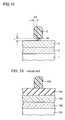
- FIG. 13 is a cross sectional view shown in conjunction with a step of a conventional method of manufacturing a semiconductor device.
- FIGS. 14 and 15 are cross sectional views respectively shown in conjunction with steps performed after the steps shown in FIGS. 13 and 14 .
- a method of manufacturing a semiconductor device will be described.
- a polycrystalline silicon film 2 is formed on a silicon substrate 1 for example by CVD.
- a tungsten silicide film 3 is formed on polycrystalline silicon film 2 for example by sputtering.
- An insulating film 4 such as a silicon oxide film which is to be a hard mask is formed on tungsten silicide film 3 .
- a photoresist pattern 5 is formed on insulating film 4 .
- a hard mask 4 b is formed having a desired dimension.
- photoresist pattern 5 covering hard mask 4 b is removed.
- photoresist pattern 5 covering hard mask 4 b is removed.
- an interconnection 6 including polycrystalline silicon film 2 a and tungsten silicide film 3 a is formed.
- interconnection 6 an interconnection of a polycide structure including polycrystalline silicon film 2 a and tungsten silicide film 3 a has been described by way of example as interconnection 6 , the method of manufacturing the semiconductor device can also be applied to an interconnection including a metal film such as a tungsten film or that including only a polycrystalline silicon film.
- silicon oxide film is used as the layer to be hard mask 4 b in the present embodiment
- a silicon nitride film may also be applied.
- etching can be performed with high selectivity along the main surface of silicon substrate 1 with respect to underlying tungsten silicide film 3 .
- a fluorocarbon based polymer film (not shown) is formed on the exposed side surface insulating film 4 a .
- the polymer film can uniformly be removed.
- hard mask 4 b can be formed with higher dimensional accuracy. It is noted that the etching of the polymer film will be described in greater detail in the second embodiment section.
- photoresist pattern 5 is directly formed on insulating film 4 including the silicon oxide film, as shown in FIG. 1 or the like. If a design rule decreases to at most 0.3 ⁇ m, it becomes difficult to accurately patterning the photoresist pattern on the silicon oxide film due to lithography characteristic.
- an anti-reflection film (ARC) is applied.
- ARC anti-reflection film
- a method of manufacturing the semiconductor device with application of the anti-reflection film will be described.
- an inorganic anti-reflection film such as a plasma nitride film is particularly described by way of example.
- an anti-reflection film 7 (not shown) such as a silicon nitride film is formed after insulating film 4 is formed. Thereafter, as shown in FIG. 6, a photoresist is applied onto anti-reflection film 7 and a desired photoresist pattern 5 is formed.
- tungsten silicide film 3 is exposed and insulating film 4 a is formed.
- a fluorocarbon based polymer film 8 is formed on the exposed side surface of insulating film 4 a.
- photoresist pattern 5 positioned on anti-reflection film 7 is removed.
- hard mask 4 b is formed. It is noted that, polymer film 8 is uniformly removed if a pressure of the gas phase hydrofluoric acid ambient is set in a range of several kPa to several tens of kPa.
- anti-reflection film 7 is removed by wet etching or dry etching.
- an interconnection 6 including polycrystalline silicon film 2 a and tungsten silicide film 3 a is formed as shown in FIG. 5 shown in conjunction with the first embodiment.
- the step shown in conjunction with FIG. 7 has been described as performing etching with a pressure of the gas phase hydrofluoric acid ambient being maintained at several kPa to several tens of kPa.
- three patterns of relationships between the pressure and the etching time can be obtained for example as shown in FIGS. 8 to 10 .
- the pressure gradually increases over the etching time.
- the pressure changes in a serrated form over the etching time.
- the pressure increases at the start of etching and then maintained at a constant value.
- a maximum pressure p corresponds to the above mentioned pressure of the gas phase hydrofluoric acid in the first and third patterns, whereas a pressure p, i.e., average pressure overtime, corresponds to that in the second pattern.
- anti-reflection film 7 can be removed by wet etching using a solution including thermal phosphoric acid with a small amount of hydrofluoric acid. If a gas including CHF 3 , CF 4 , Ar and O 2 is used, anti-reflection film 7 can be removed by dry etching. Further, in the method using dry etching, an anti-reflection film including a silicon nitride film can be removed.
- a method of manufacturing a semiconductor device according to the third embodiment of the present invention will be described.
- etching must be performed twice to form hard mask 4 b .
- a method of forming a hard mask only by one etching will be described.
- an insulating film 4 with a prescribed thickness is formed on tungsten silicide film 3 .
- a photoresist pattern 5 is formed on insulating film 4 . It is noted that the prescribed thickness of insulating film 4 will later be described.
- insulating film 4 is isotropically etched using photoresist pattern 5 as a mask in a gas phase hydrofluoric acid ambient.
- a hard mask 4 b is formed under photoresist pattern 5 as shown in FIG. 12 .
- photoresist pattern 5 is removed, and tungsten silicide film 3 and polycrystalline silicon film 2 are anisotropically etched using hard mask 4 b as a mask, so that a desired interconnection (not shown) is formed.
- a semiconductor device having a fine interconnection is formed.
Landscapes
- Drying Of Semiconductors (AREA)
- Internal Circuitry In Semiconductor Integrated Circuit Devices (AREA)
Abstract
Description
Claims (19)
Applications Claiming Priority (2)
| Application Number | Priority Date | Filing Date | Title |
|---|---|---|---|
| JP2000037764A JP2001230233A (en) | 2000-02-16 | 2000-02-16 | Method for manufacturing semiconductor device |
| JP2000-037764 | 2000-02-16 |
Publications (1)
| Publication Number | Publication Date |
|---|---|
| US6593243B1 true US6593243B1 (en) | 2003-07-15 |
Family
ID=18561605
Family Applications (1)
| Application Number | Title | Priority Date | Filing Date |
|---|---|---|---|
| US09/632,163 Expired - Fee Related US6593243B1 (en) | 2000-02-16 | 2000-08-03 | Method of manufacturing semiconductor device |
Country Status (4)
| Country | Link |
|---|---|
| US (1) | US6593243B1 (en) |
| JP (1) | JP2001230233A (en) |
| KR (1) | KR100374955B1 (en) |
| TW (1) | TW471069B (en) |
Cited By (3)
| Publication number | Priority date | Publication date | Assignee | Title |
|---|---|---|---|---|
| US20040253829A1 (en) * | 2003-06-14 | 2004-12-16 | Peter Friis | Methods to planarize semiconductor device and passivation layer |
| US20080233730A1 (en) * | 2007-03-23 | 2008-09-25 | Hynix Semiconductor Inc. | Method for fabricating semiconductor device |
| CN108962746A (en) * | 2017-05-25 | 2018-12-07 | 南亚科技股份有限公司 | patterning method |
Families Citing this family (5)
| Publication number | Priority date | Publication date | Assignee | Title |
|---|---|---|---|---|
| KR20040005385A (en) * | 2002-07-10 | 2004-01-16 | 주식회사 하이닉스반도체 | Method for forming gate in semiconductor device |
| KR101009005B1 (en) * | 2003-06-18 | 2011-01-17 | 주식회사 포스코 | Central Alignment and Entry Device of Mailing Needle in Annealing Furnace |
| KR100955926B1 (en) * | 2003-06-27 | 2010-05-03 | 주식회사 하이닉스반도체 | Metal wiring formation method of semiconductor device |
| KR100714287B1 (en) * | 2005-02-25 | 2007-05-02 | 주식회사 하이닉스반도체 | Pattern formation method of semiconductor device |
| KR100948093B1 (en) * | 2007-12-21 | 2010-03-16 | 주식회사 하이닉스반도체 | Semiconductor device and manufacturing method thereof |
Citations (12)
| Publication number | Priority date | Publication date | Assignee | Title |
|---|---|---|---|---|
| JPH05160081A (en) | 1991-06-03 | 1993-06-25 | Sony Corp | Dry etching method |
| JPH06275574A (en) | 1993-03-18 | 1994-09-30 | Sony Corp | Dry etching method |
| US5429070A (en) * | 1989-06-13 | 1995-07-04 | Plasma & Materials Technologies, Inc. | High density plasma deposition and etching apparatus |
| US5472564A (en) * | 1988-02-09 | 1995-12-05 | Fujitsu Limited | Method of dry etching with hydrogen bromide or bromide |
| JPH0817330A (en) | 1993-07-16 | 1996-01-19 | Matsushita Electric Ind Co Ltd | Field emission electron source and method of manufacturing the same |
| US5541127A (en) * | 1991-04-17 | 1996-07-30 | Mitsubishi Denki Kabushiki Kaisha | Manufacturing method of sidewall insulating film |
| US5856227A (en) * | 1997-05-01 | 1999-01-05 | Taiwan Semiconductor Manufacturing Company, Ltd. | Method of fabricating a narrow polycide gate structure on an ultra-thin gate insulator layer |
| US5930594A (en) * | 1995-07-13 | 1999-07-27 | Commissariat A L'energie | Method of manufacturing rigid floating microstructure elements and a device equipped with such elements |
| US6004853A (en) * | 1999-05-27 | 1999-12-21 | Vanguard International Semiconductor Corporation | Method to improve uniformity and the critical dimensions of a DRAM gate structure |
| US6235638B1 (en) * | 1999-02-16 | 2001-05-22 | Micron Technology, Inc. | Simplified etching technique for producing multiple undercut profiles |
| US6261934B1 (en) * | 1998-03-31 | 2001-07-17 | Texas Instruments Incorporated | Dry etch process for small-geometry metal gates over thin gate dielectric |
| US6316166B1 (en) * | 1998-06-30 | 2001-11-13 | Hyundai Electronics Industries Co., Ltd. | Method of forming micro pattern of semiconductor device |
-
2000
- 2000-02-16 JP JP2000037764A patent/JP2001230233A/en not_active Withdrawn
- 2000-08-03 US US09/632,163 patent/US6593243B1/en not_active Expired - Fee Related
- 2000-10-13 TW TW089121433A patent/TW471069B/en not_active IP Right Cessation
- 2000-10-20 KR KR10-2000-0061871A patent/KR100374955B1/en not_active Expired - Fee Related
Patent Citations (12)
| Publication number | Priority date | Publication date | Assignee | Title |
|---|---|---|---|---|
| US5472564A (en) * | 1988-02-09 | 1995-12-05 | Fujitsu Limited | Method of dry etching with hydrogen bromide or bromide |
| US5429070A (en) * | 1989-06-13 | 1995-07-04 | Plasma & Materials Technologies, Inc. | High density plasma deposition and etching apparatus |
| US5541127A (en) * | 1991-04-17 | 1996-07-30 | Mitsubishi Denki Kabushiki Kaisha | Manufacturing method of sidewall insulating film |
| JPH05160081A (en) | 1991-06-03 | 1993-06-25 | Sony Corp | Dry etching method |
| JPH06275574A (en) | 1993-03-18 | 1994-09-30 | Sony Corp | Dry etching method |
| JPH0817330A (en) | 1993-07-16 | 1996-01-19 | Matsushita Electric Ind Co Ltd | Field emission electron source and method of manufacturing the same |
| US5930594A (en) * | 1995-07-13 | 1999-07-27 | Commissariat A L'energie | Method of manufacturing rigid floating microstructure elements and a device equipped with such elements |
| US5856227A (en) * | 1997-05-01 | 1999-01-05 | Taiwan Semiconductor Manufacturing Company, Ltd. | Method of fabricating a narrow polycide gate structure on an ultra-thin gate insulator layer |
| US6261934B1 (en) * | 1998-03-31 | 2001-07-17 | Texas Instruments Incorporated | Dry etch process for small-geometry metal gates over thin gate dielectric |
| US6316166B1 (en) * | 1998-06-30 | 2001-11-13 | Hyundai Electronics Industries Co., Ltd. | Method of forming micro pattern of semiconductor device |
| US6235638B1 (en) * | 1999-02-16 | 2001-05-22 | Micron Technology, Inc. | Simplified etching technique for producing multiple undercut profiles |
| US6004853A (en) * | 1999-05-27 | 1999-12-21 | Vanguard International Semiconductor Corporation | Method to improve uniformity and the critical dimensions of a DRAM gate structure |
Cited By (5)
| Publication number | Priority date | Publication date | Assignee | Title |
|---|---|---|---|---|
| US20040253829A1 (en) * | 2003-06-14 | 2004-12-16 | Peter Friis | Methods to planarize semiconductor device and passivation layer |
| US6987068B2 (en) * | 2003-06-14 | 2006-01-17 | Intel Corporation | Methods to planarize semiconductor device and passivation layer |
| US20080233730A1 (en) * | 2007-03-23 | 2008-09-25 | Hynix Semiconductor Inc. | Method for fabricating semiconductor device |
| CN108962746A (en) * | 2017-05-25 | 2018-12-07 | 南亚科技股份有限公司 | patterning method |
| CN108962746B (en) * | 2017-05-25 | 2020-10-09 | 南亚科技股份有限公司 | patterning method |
Also Published As
| Publication number | Publication date |
|---|---|
| TW471069B (en) | 2002-01-01 |
| KR20010081947A (en) | 2001-08-29 |
| JP2001230233A (en) | 2001-08-24 |
| KR100374955B1 (en) | 2003-03-06 |
Similar Documents
| Publication | Publication Date | Title |
|---|---|---|
| KR100381885B1 (en) | Method of manufacturing semiconductor device having minute gate electrodes | |
| US5994234A (en) | Method for dry-etching a polycide film | |
| JP2004519838A (en) | Method for etching titanium nitride | |
| JPH05136105A (en) | Method for selectively etching surface of structure | |
| US7307009B2 (en) | Phosphoric acid free process for polysilicon gate definition | |
| US6399286B1 (en) | Method of fabricating reduced critical dimension for conductive line and space | |
| US6593243B1 (en) | Method of manufacturing semiconductor device | |
| JP3088178B2 (en) | Polysilicon film etching method | |
| US6211557B1 (en) | Contact structure using taper contact etching and polycide step | |
| JP3312604B2 (en) | Method for manufacturing semiconductor device | |
| JP2822952B2 (en) | Method for manufacturing semiconductor device | |
| JPH08321484A (en) | Method for manufacturing semiconductor device | |
| TW200532800A (en) | Method for fabricating a hard mask polysilicon gate | |
| JPH0346252A (en) | Semiconductor integrated circuit and manufacture | |
| US6743726B2 (en) | Method for etching a trench through an anti-reflective coating | |
| JP2004363371A (en) | Method of manufacturing electronic device | |
| JPH11330045A (en) | Etching method for laminated film of oxide film and silicon layer | |
| KR100587039B1 (en) | Contact hole formation method of semiconductor device | |
| JPH09321024A (en) | Method for manufacturing semiconductor device | |
| US20030064599A1 (en) | Pattern forming method | |
| JP2002141328A (en) | Semiconductor device and manufacturing method thereof | |
| JP3067739B2 (en) | Etching method | |
| KR100223265B1 (en) | Contact hole formation method of semiconductor device | |
| KR100465638B1 (en) | Etching Method of Semiconductor Device | |
| KR19990065142A (en) | Method for forming vertical profile pattern of material layer containing silicon |
Legal Events
| Date | Code | Title | Description |
|---|---|---|---|
| AS | Assignment |
Owner name: MITSUBISHI DENKI KABUSHIKI KAISHA, JAPAN Free format text: (ASSIGNMENT OF ASSIGNOR'S INTEREST) RE-RECORD TO CORRECT THE RECORDATION DATE OF 08/30/2000 TO 08/03/2000 PREVIOUSLY RECORDED AT REEL 11127 FRAME 0613.;ASSIGNOR:KIMURA, HAJIME;REEL/FRAME:011303/0290 Effective date: 20000630 |
|
| AS | Assignment |
Owner name: MITSUBISHI DENKI KABUSHIKI KAISHA, JAPAN Free format text: INVALID ASSIGNMENT;ASSIGNOR:KIMURA, HAJIME;REEL/FRAME:011127/0613 Effective date: 20000630 |
|
| FEPP | Fee payment procedure |
Free format text: PAYOR NUMBER ASSIGNED (ORIGINAL EVENT CODE: ASPN); ENTITY STATUS OF PATENT OWNER: LARGE ENTITY |
|
| FPAY | Fee payment |
Year of fee payment: 4 |
|
| FPAY | Fee payment |
Year of fee payment: 8 |
|
| AS | Assignment |
Owner name: RENESAS ELECTRONICS CORPORATION, JAPAN Free format text: ASSIGNMENT OF ASSIGNORS INTEREST;ASSIGNOR:MITSUBISHI DENKI KABUSHIKI KAISHA;REEL/FRAME:025980/0219 Effective date: 20110307 |
|
| REMI | Maintenance fee reminder mailed | ||
| LAPS | Lapse for failure to pay maintenance fees | ||
| STCH | Information on status: patent discontinuation |
Free format text: PATENT EXPIRED DUE TO NONPAYMENT OF MAINTENANCE FEES UNDER 37 CFR 1.362 |
|
| FP | Lapsed due to failure to pay maintenance fee |
Effective date: 20150715 |