US6541908B1 - Electronic light emissive displays incorporating transparent and conductive zinc oxide thin film - Google Patents
Electronic light emissive displays incorporating transparent and conductive zinc oxide thin film Download PDFInfo
- Publication number
- US6541908B1 US6541908B1 US09/410,130 US41013099A US6541908B1 US 6541908 B1 US6541908 B1 US 6541908B1 US 41013099 A US41013099 A US 41013099A US 6541908 B1 US6541908 B1 US 6541908B1
- Authority
- US
- United States
- Prior art keywords
- cathode
- anode
- work function
- display
- emissive
- Prior art date
- Legal status (The legal status is an assumption and is not a legal conclusion. Google has not performed a legal analysis and makes no representation as to the accuracy of the status listed.)
- Expired - Fee Related
Links
Images


Classifications
-
- H—ELECTRICITY
- H01—ELECTRIC ELEMENTS
- H01J—ELECTRIC DISCHARGE TUBES OR DISCHARGE LAMPS
- H01J1/00—Details of electrodes, of magnetic control means, of screens, or of the mounting or spacing thereof, common to two or more basic types of discharge tubes or lamps
- H01J1/02—Main electrodes
- H01J1/30—Cold cathodes, e.g. field-emissive cathode
- H01J1/304—Field-emissive cathodes
-
- H—ELECTRICITY
- H10—SEMICONDUCTOR DEVICES; ELECTRIC SOLID-STATE DEVICES NOT OTHERWISE PROVIDED FOR
- H10K—ORGANIC ELECTRIC SOLID-STATE DEVICES
- H10K50/00—Organic light-emitting devices
- H10K50/80—Constructional details
- H10K50/805—Electrodes
- H10K50/82—Cathodes
- H10K50/828—Transparent cathodes, e.g. comprising thin metal layers
-
- H—ELECTRICITY
- H10—SEMICONDUCTOR DEVICES; ELECTRIC SOLID-STATE DEVICES NOT OTHERWISE PROVIDED FOR
- H10K—ORGANIC ELECTRIC SOLID-STATE DEVICES
- H10K59/00—Integrated devices, or assemblies of multiple devices, comprising at least one organic light-emitting element covered by group H10K50/00
-
- H—ELECTRICITY
- H10—SEMICONDUCTOR DEVICES; ELECTRIC SOLID-STATE DEVICES NOT OTHERWISE PROVIDED FOR
- H10K—ORGANIC ELECTRIC SOLID-STATE DEVICES
- H10K59/00—Integrated devices, or assemblies of multiple devices, comprising at least one organic light-emitting element covered by group H10K50/00
- H10K59/80—Constructional details
- H10K59/805—Electrodes
- H10K59/8052—Cathodes
- H10K59/80524—Transparent cathodes, e.g. comprising thin metal layers
-
- H—ELECTRICITY
- H10—SEMICONDUCTOR DEVICES; ELECTRIC SOLID-STATE DEVICES NOT OTHERWISE PROVIDED FOR
- H10K—ORGANIC ELECTRIC SOLID-STATE DEVICES
- H10K2102/00—Constructional details relating to the organic devices covered by this subclass
- H10K2102/301—Details of OLEDs
- H10K2102/302—Details of OLEDs of OLED structures
- H10K2102/3023—Direction of light emission
- H10K2102/3026—Top emission
-
- H—ELECTRICITY
- H10—SEMICONDUCTOR DEVICES; ELECTRIC SOLID-STATE DEVICES NOT OTHERWISE PROVIDED FOR
- H10K—ORGANIC ELECTRIC SOLID-STATE DEVICES
- H10K2102/00—Constructional details relating to the organic devices covered by this subclass
- H10K2102/301—Details of OLEDs
- H10K2102/302—Details of OLEDs of OLED structures
- H10K2102/3023—Direction of light emission
- H10K2102/3031—Two-side emission, e.g. transparent OLEDs [TOLED]
-
- H—ELECTRICITY
- H10—SEMICONDUCTOR DEVICES; ELECTRIC SOLID-STATE DEVICES NOT OTHERWISE PROVIDED FOR
- H10K—ORGANIC ELECTRIC SOLID-STATE DEVICES
- H10K50/00—Organic light-emitting devices
- H10K50/80—Constructional details
- H10K50/87—Arrangements for heating or cooling
-
- H—ELECTRICITY
- H10—SEMICONDUCTOR DEVICES; ELECTRIC SOLID-STATE DEVICES NOT OTHERWISE PROVIDED FOR
- H10K—ORGANIC ELECTRIC SOLID-STATE DEVICES
- H10K59/00—Integrated devices, or assemblies of multiple devices, comprising at least one organic light-emitting element covered by group H10K50/00
- H10K59/80—Constructional details
- H10K59/87—Passivation; Containers; Encapsulations
- H10K59/873—Encapsulations
Definitions
- the present invention relates to the applications of co-coped n-type zinc oxide thin film as a chemically stable and low work function cathode to Organic Light Emissive Diode (OLED) display, Field Emission Display (FED) and vacuum microelectronic display devices.
- OLED Organic Light Emissive Diode
- FED Field Emission Display
- Display devices are a fast growing segment of the electronics market. Historically, commercially viable displays have relied on cathode ray tube (CRT) and liquid crystal display (LCD) technologies due to reliability and affordability. CRT technology is mature and able to achieve high resolution, high luminance (brightness), low cost and long life. Unfortunately, CRT displays require high operating voltages and are too heavy for portable applications. CRTs also have a large bulky form factor. More recently, flat panel LCDs have gained acceptance in many applications since they operate at power levels compatible with battery operation, are lightweight and have a thin form factor. LCD panels either reflect or transmit light so an external light source is required. LCD panels also have a limited viewing angle so the user may not be able to see the displayed information from an oblique viewing angle.
- CTR cathode ray tube
- LCD liquid crystal display
- LCD displays Although the viewing angle for LCD displays has improved over the years, they are still inferior compared to CRTs and other emissive display technologies. Another weakness of LCD displays is that the liquid crystal material response to a stimulus is intrinsically slow at low temperatures. Thus, LCD displays are a poor choice for portable, automotive or military applications where operation at extreme low temperature may be required. Accordingly, there is great need for an inexpensive low-power display technology that exhibits real-time imaging capability in the flat panel form factor over an extended operating temperature range.
- Light emissive devices have a form factor of an LCD display but are not dependent on external light sources. Emissive devices also have the wide viewing angle of a CRT and will operate over an extended temperature range.
- Two examples of emissive devices are the organic light emitting diode (OLED) display devices and the field effect display devices.
- OLED organic light emitting diode
- Emissive display devices are lightweight and capable of projecting video rate images with high contrast ratio over an extended temperature range. Emissive displays hold great promise as an alternative to LCDs because they have superior viewing angle characteristics and high video rates.
- the response rate of emissive displays is not affected by a low ambient operating temperature.
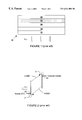
- FIG. 1 illustrates a portion of a prior art OLED device 10 .
- Device 10 has an opaque cathode electrode 12 in a spaced-apart arrangement with a transparent anode electrode 14 deposited on a transparent substrate 18 .
- An organic emissive medium 20 is sandwiched between cathode electrode 12 and an anode electrode 14 with pixels defined wherever the cathode electrode overlaps the anode electrode.
- Layer 23 may be applied over cathode electrode 12 to encapsulate device 10 and protect the device.
- the cathode electrode 12 is usually an opaque reflective low work function metal such as an alkaline earth metal or reactive metal alloy. Examples of prior art cathode electrodes include calcium, magnesium/silver, or aluminum/lithium.
- the anode electrode 14 is a high work function thin film of transparent indium tin oxide (ITO).
- ITO transparent indium tin oxide
- work function refers to the energy difference, in electron volts (eV), between a free electron and an electron at the Fermi level of the material.
- Fermi level indicates the energy level at which the probability that a state of energy is occupied is equal to one half.
- the work function of the cathode needs to be low so that the Fermi level closely matches the energy level of the lowest unoccupied molecular orbital (LUMO) of the organic medium.
- the work function of the anode needs to closely match the energy level of the highest occupied molecular orbital (HOMO) of the organic medium.
- ITO is the material of choice for the transparent anode
- prior art research has focused on use of alkaline earth metal cathodes having a low work function to achieve device efficiency.
- alkaline earth metals are extremely reactive and are not transparent.
- FIG. 2 illustrates the potential energy diagram of the prior art OLED device illustrated in FIG. 1 .
- the Fermi level of the ITO (work function is about 4.7 eV as indicated at 22 ) is above the HOMO energy level of the organic medium.
- the HOMO is about 4.9 eV for the MEH-PPV organic polymer
- energy is required to inject holes, represented by h + , over the potential energy barrier into the organic medium.
- the Fermi level of the metal cathode (about 3 eV to 4 eV for typical alkaline earth metals as indicated at 24 ) is below the LUMO of the medium (about 2.8 eV), so energy is also required to inject electrons, represented by e ⁇ , into medium 20 .
- the operating voltage must be sufficient to overcome the potential barriers to inject both electrons and holes into the medium before light will be generated.
- the imbalance in the ratio of hole injection and electron injection generates heat dissipation. Such heating contributes to degradation of the medium and low efficiency of the OLED device.
- ITO transparent electrode
- a reactive low work function metal as the cathode
- OLED device design to the traditional architecture illustrated in FIG. 1 .
- One example is a miniature OLED display integrated monolithically with the driving circuit on a silicon substrate.
- This device requires that the opaque reactive metal cathode (Ca, Mg) be deposited on the silicon backplane and the ITO anode to be deposited on the organic emissive medium.
- the reactive cathode readily oxidizes and may degrade the organic medium interface.
- reactive metals are not compatible with the semiconductor processing technology and can degrade driving circuits on silicon substrates.
- Field emission display (FED) devices represent another type of emissive display that is similar to traditional CRT display technology in that an independently addressable stream of electrons excites each pixel.
- CRT uses a single electron source to sweep a single beam of electrons across the back of a phosphor screen
- FED devices incorporate an array of emitters (the cathodes), each of which ejects a stream of electrons in the presence of an applied electric field to excite a corresponding pixel on an opposing display surface (the anode).
- Each emitter in a FED device has a pyramidal or a conical top terminating in a sharp point coupled at the base to a cathode electrode.
- a control gate resides just above each emitter or group of emitters. Applying a voltage between each individually addressable gate and cathode electrode results in a steam of electrons, which excites a phosphor at the anode, thus resulting in visible light being generated.
- the anode electrode sets the bias voltage to attract the electron stream but need not be otherwise addressable.
- prior art FEDs have an unacceptably short operational lifetime and require high operating voltages due to various material limitations related to the emitters. Most of the prior art FEDs have emitters that are made from materials such as silicon and refractory metals.
- the present invention relates the use of co-doped zinc oxide (n-type) as the cathode of organic light emitting diode (OLED) displays, field emission displays (FEDs) and vacuum microelectronic devices.
- OLED organic light emitting diode
- FEDs field emission displays
- the invention overcomes the limitations in the prior art described above and other limitations in the prior art that will become apparent upon reading and understanding this specification.
- the present invention maximizes device efficiency, improves device reliability and extends the flexibility to new device architectures.
- a co-doped zinc oxide film is deposited on a glass substrate.
- An emissive organic medium is sandwiched between the co-doped (n-type) zinc oxide cathode and an anode made with high work function metals such as gold (Au), platinum (Pt) or nickel (Ni).
- Au gold
- Pt platinum
- Ni nickel
- Light transmits through the zinc oxide cathode and the glass substrate.
- This device uses a low work function cathode and high work function anode to minimize the electron injection and hole injection energy barrier to maximize device efficiency.
- a bi-directional OLED display has an emissive organic medium sandwiched between a transparent indium tin oxide (ITO) anode and a transparent co-doped zinc oxide cathode. Since both electrodes are transparent, light emits bi-directionally from both the top and the bottom of the device.
- the co-doped zinc oxide cathode has a low work function that minimizes the potential energy barrier to inject electrons from the cathode into the organic medium so the display device operates more efficiently. Since the co-doped zinc oxide thin film can be deposited at a low temperature, it can be deposited on the organic emissive medium without degrading the medium. This low temperature deposition process is preferred to fabricate any OLED device where the transparent ZnO cathode is not deposited on a glass substrate.
- the anode is a high work function metal, such as platinum (Pt) or gold (Au).
- the reflective, high work function metal anode minimizes the potential barrier to inject holes into the organic medium and provides an improved unidirectional display.
- the non-reactive metal anode may be deposited on silicon or another substrate with a co-doped zinc oxide as the transparent electrode (cathode) deposited and patterned on top of an organic layer. Since both electrodes are non-reactive, an emissive display device may be combined with control electronics on a single substrate. This embodiment is particularly useful for miniature display applications. Miniature flat-panel displays on silicon permit the integration of display drive electronics with the display on a common substrate. This type of miniature display provides high resolution and low cost particularly desired for wireless or mobile applications where low power and high efficiency can minimize weight and increase battery life.
- the low work function and chemical robustness of the co-doped zinc oxide electrode also hold application as a field emitting material for FEDs and vacuum microelectronic devices.
- the present invention provides improved resistance to cathode oxidation common in prior art displays.
- the invention also provides high operation efficiency because of the low work function of the material.
- a thin film of co-doped zinc oxide is deposited on the emitter surface of FED devices or vacuum microelectronic devices. This coating minimizes performance degradation induced by surface oxidation of the emitters and enhances electron emission efficiency due to the low work function of this material.
- Another embodiment describes a field emission light source.
- a plurality of transparent zinc oxide emitters is fabricated on a transparent substrate and a phosphor layer is applied to a metal anode.
- An electric field is applied between the emitter and the phosphor to accelerate electron streams toward the anode and bombard onto the phosphor.
- Light generated on the phosphor layer will transmit through the transparent cathode.
- heat generated during the interaction between the electron streams and phosphor is dissipated in the metal anode.
- the high thermal conductivity of the metal anode effectively removes the heat and enables high power operation to result in high light intensity output.
- FIG. 1 illustrates a typical prior art organic light emission device having a metal cathode and an ITO anode
- FIG. 2 illustrates the band diagram of a typical prior art OLED device depicting the potential energy barriers to injecting electrons and holes;
- FIG. 3 illustrates a schematic representation of one embodiment of an OLED device having a co-doped zinc oxide cathode on glass substrate and a high work function metal anode;
- FIG. 4 illustrates a schematic representation of an OLED device having a high work function metal anode on a glass substrate and a co-doped zinc oxide thin film cathode;
- FIG. 5 illustrates a schematic representation of an OLED on a silicon substrate with monolithically integrated electronic driving circuits
- FIG. 6 illustrates a potential energy barrier diagram for an OLED device having the co-doped zinc oxide thin film cathode and a high work function anode of the present invention
- FIG. 7 illustrates a schematic representation of an OLED having an ITO anode on a glass substrate and a co-doped zinc oxide cathode
- FIG. 8 illustrates a schematic representation of a single pixel of a FED device.
- FIGS. 9A, 9 B and 9 C illustrate various alternative structures for one emitter of the FED device of FIG. 8 with each emitter having a co-doped zinc oxide coating;
- FIG. 10 illustrates another schematic representation of a second embodiment of a field emission light source of the present invention.
- the present invention relates to improved display technologies.
- the principles of the invention are illustrated and embodied in various emissive display systems suitable for use in generating a displayed image.
- the lightweight display systems have a small form factor, high resolution, high luminance (brightness), and long operating lifetime.
- Co-doped zinc oxide thin films that simultaneously incorporate gallium and hydrogen atoms as electron donors can address the material needs in aforementioned sections.
- the properties of co-doped zinc oxide thin film are described in a co-pending application entitled Transparent and Conductive Zinc Oxide Film with Low Growth Temperature, U.S. Ser. No. 09/281198 filed Mar. 30, 1999 assigned to Rockwell Science Center, LLC, the assignee of the present application by Jeffrey T. Cheung, a co-inventor of the present invention.
- the co-doped zinc oxide has a lower growth temperature, is compatible with OLED processing, and has a high electron concentration that results in a substantial raising of the Fermi level to achieve a low work function. All these properties are desirable to improve the performance of OLED, FED, and vacuum microelectronic devices.
- cathode 30 comprises a thin film of co-doped zinc oxide deposited on a transparent substrate 32 .
- co-doped means that the zinc oxide thin film is doped with both gallium (Ga) and hydrogen (H) as described in the above-referenced co-pending application.
- the cathode thin film is patterned using etching techniques or by deposition through a shadow mask.
- Substrate 32 is typically a soda lime glass substrate capable of withstanding deposition and processing temperatures in excess of 200° C.
- the flexible substrate may be selected from a group consisting of acrylics, urethanes, polystyrenes, polycarbonates, styrene-acrylonitrile copolymers, styrene-butadiene copolymers, cellulosics, acrylonitrile-butadiene-styrene, polyvinylchloride, thermoplastic polyesters, polypropylene, nylons, polyester carbonates, ionomers, polyethyleneterephthate, and cyclic olefin copolymers.
- This wide range of substrate material enables the customization of the emissive display device to suit the application environment or price requirements.
- organic medium 20 is deposited on top of cathode 30 .
- wet chemical deposition or vacuum deposition may be used to deposit medium 20 , it being recognized that the selected medium may determine the optimal deposition technique. If necessary, the medium is treated to evacuate any volatile solvents or impurities that may be introduced by the deposition technique.
- the thickness of medium 20 is an engineering consideration dependent on the particular choice of medium 20 and on the intended application. In most applications, the medium will be about 1,000 Angstroms thick.
- Medium 20 may be selected from known light emissive organic polymers, such as MEH-PPV, or small molecules, such as aluminum 8-hydroxyquinoline (Alq 3 ) or dye-doped Alq 3 .
- Fluorescent metal chelate complexes or other suitable emissive organic materials may also be suitable for some applications as the light-emitting medium.
- medium 20 may comprise a hole transport layer, such as a tetraarylbenzidine derivative (TPD) or a TPD derivative (NPB), disposed proximate to the anode and an electron transport layer, such as Alq 3 disposed proximate to the cathode.
- TPD tetraarylbenzidine derivative
- NPB TPD derivative
- Alq 3 disposed proximate to the cathode.
- two layers are used to force recombination at the layers' interface rather than at one of the electrodes.
- the potential energy barriers at both electrodes are minimized so the display device will have substantially equal injection of holes and electrons. This balancing of charge carriers maximizes the possibility that carriers will recombine radiatively, thereby minimizing power dissipation since fewer carriers travel through the medium without combining to generate light.
- anode 34 is then deposited so that medium 20 is sandwiched between the anode and the cathode.
- Deposition of the anode may be by way of vacuum deposition at low temperatures, by example, below 50° C. although other deposition techniques are known and may be used.
- anode 34 comprises a thin film of gold (Au), platinum (Pt) or nickel (Ni). More specifically, the anode is selected from metals having a Fermi level that is equal to or below the Highest Occupied Molecular Orbital (HOMO) energy level of the organic medium 20 .
- HOMO Highest Occupied Molecular Orbital
- anode 34 is patterned such that the relationship between the cathode and anode electrodes will cooperate to form the desired pattern. Patterning is preferably performed using well-known semiconductor processing techniques such as a shadow mask.
- An encapsulating layer 36 is deposited on top of anode 34 to provide some protection from the environment.
- FIG. 4 illustrates another preferred embodiment of a display in accordance with the present invention.
- Display device 40 is shown having a co-doped zinc oxide cathode 30 and emissive medium 20 .
- the anode 34 which is deposited on substrate 32 , is a high work function metal such as described above.
- a metal contact 38 preferably aluminum, is deposited and patterned on cathode 30 to make ohmic contact with the co-doped zinc oxide.
- a transparent encapsulating layer 36 is deposited to cover the metal contact and the exposed cathode to protect the device from the environment. Light generated in the organic medium transmits through the cathode.
- FIG. 5 Another embodiment, illustrated in FIG. 5, is a miniature emissive display formed on a silicon substrate 42 containing an integrated circuit (not illustrated).
- the integrated circuit is created using standard semiconductor processing techniques well known in the art.
- a layer of insulating oxide (not shown) is deposited and patterned on top of the substrate, the elements of display 50 are deposited and patterned.
- a high work function metal anode 34 is deposited on the substrate. More specifically, the anode is selected from metals that do not interact with silicon at temperature lower than 200° C. and have a Fermi level that is close to or below the HOMO energy level of the medium 20 .
- Gold (Au) and platinum (Pt) are particularly well suited for this anode material.
- Connection between the integrated circuit and the anode is made by providing vias through the oxide layer to the top layer of metal of the integrated circuit.
- Organic emissive medium 20 is then sandwiched between the anode and co-doped zinc oxide cathode 30 .
- Aluminum ohmic contacts 38 are deposited and patterned on cathode 30 . Connection between ohmic contacts 38 and the integrated circuit may be by wire-bonding or other metal interconnect means.
- An encapsulating layer 36 protects the device from environment. This device is a miniature emissive display integrated monolithically with the driving circuit on silicon substrate. Magnifying lenses may be attached or positioned in alignment with the display to enlarge the viewing area perceived by the viewer.
- FIG. 6 the potential barriers associated with display devices 40 and 50 is shown.
- the use of the co-doped zinc oxide cathode and the high work function metal anode facilitates alignment of the Fermi levels of the anode and cathode with the LUMO and HOMO of the organic medium, respectively.
- the result minimizes or reduces the hole and electron transport barriers. Removing these barriers permits a lower operating voltage and higher efficiency.
- the lower operating voltage minimizes internal heat generation and should improve the life span of the display.
- inexpensive, efficient and lightweight light emissive displays are now possible in a small form factor.
- FIG. 7 Another embodiment, a bi-directional OLED device, is illustrated in FIG. 7 .
- the term “bi-directional” means light emissions transmit through both the anode and the cathode.
- anode comprises a thin film of ITO 14 deposited on a transparent substrate 32 . Once anode 14 is patterned, organic medium 20 is deposited on top of anode 14 . The manner of deposition, and selection of the thickness of medium 20 is an engineering consideration dependent on the particular choice of medium 20 and on the intended application as previously described.
- Cathode 30 comprises a co-doped zinc oxide film that is deposited on medium 20 .
- cathode 30 is patterned such that the relationship between the anode and the cathode electrodes will cooperate to form the desired pattern. Patterning is preferably performed using well-known semiconductor processing techniques such as a shadow mask.
- a contact layer 38 is deposited on cathode 30 and then patterned, again using known patterning and etching techniques to form contacts 38 . Contacts 38 may be aluminum, or other materials that form ohmic contacts with co-coped zinc oxide. The contact layer material is also deposited at low temperature.
- a protective transparent passivation layer 36 is deposited on to of the contacts 38 and the exposed portion of cathode 30 to provide protection from the environment.
- Display 70 is a portion of a FED device showing a single pixel of a two-dimensional matrix or grid-like pattern. Each pixel consists of three basic components: an emitter 78 , a gate 82 , and phosphor layer 86 on the anode 88 .
- Each emitter 78 is coupled to a cathode electrode 74 by a resistive layer 76 .
- the region between emitter 78 and layer 86 forms a cavity 84 that is hermetically sealed and evacuated so that there is a vacuum between emitter 78 and phosphor layer 86 .
- a gate electrode 82 which is isolated from the emitter by insulating layer 80 , modulates the electric field applied to each emitter 78 . It controls the number of electrons, which pass from the emitter to the anode.
- the stream of electrons 92 is emitted and accelerated toward phosphor layer 86 by the electric field between cathode 74 and the anode 88 .
- Light generated by electrons impacting the phosphor is emitted through the transparent anode electrode 88 and transparent substrate 90 .
- Electron emitters are formed by a number of known processes including selective etching, selective growth, surface roughening by the bombardment of energized particles, or deposition through shadow masks.
- FIGS. 9A-9C illustrate some common shapes for the emitter such as a cone 92 , a post 94 or a sharp ridge 96 .
- Other prior art also employ emitters comprising random surface structures with sharp edge features. Regardless of the actual emitter shape, it is also desirable for the emitter material to be oxidation resistant and have a low work function. For these reasons, the preferred embodiment of the present invention includes a thin coating 98 of co-doped zinc oxide deposited on at least the top portion of emitters 92 , 94 and 96 .
- co-doped zinc oxide lowers the work function thereby improving the efficiency of the display device. Further, it is well known that during operation of display 70 of FIG. 8, residual gas and constant outgassing from the vacuum cavity surface will decrease the vacuum in region 84 over time. Without the co-doped zinc oxide coating, it is common for a layer of oxide to form on the emitters as the vacuum level decreases. This oxide layer acts as an insulator that increases the work function of the emitter and decreases the electron stream for a given field strength. This increase in work function requires a higher operating voltage to maintain a constant electron stream. It is believed that the layer of co-doped zinc oxide 98 (FIGS. 9A-9C) forms a barrier layer to oxidation. Further, the co-doped zinc oxide layer lowers the work function of the emitters, so the FED device should achieve improved emission efficiency and longer lifetime compared to silicon or metal emitters of the prior art.
- a coating of the chemically stable co-doped zinc oxide may also be incorporated in other high-density field emission applications such as silicon or tungsten cold cathodes. (that is, a stand-alone room temperature operating electron source), vacuum microelectronic devices or field emission light sources in accordance with the present invention. This coating increases the emitter's resistance to oxidation and enhances the electron emission efficiency.
- FIG. 10 discloses yet another preferred embodiment of the present invention.
- a field emission light source 100 has a phosphor layer 106 applied to a thermal conductor such as a patterned metal plate 108 and transparent co-doped zinc oxide emitters 104 deposited on a transparent substrate 102 .
- the emitters of light source 100 consist of a dense array of sharp microstructures fabricated by applying a thin film coating of co-doped zinc oxide over microstructures prefabricated on the transparent substrate.
- the emitters my comprise microstructures of thick co-doped zinc oxide film etched to obtain sharp microstructures using dry or wet etching techniques.
- emitters 104 During operation of light source 100 , emitters 104 generate streams of electrons 112 when energized. A voltage is applied between the metal anode 108 and the emitters 104 to attract and accelerate the electrons to bombard onto the phosphor 106 and generate light. Light emits through the transparent emitters. Heat generated during electron/phosphor interaction is dissipated into the metal anode which acts as a heat sink. Heat removal may be either passive by radiating from metal anode or actively, by way of example, by having coolant circulating through cooling tubes 110 attached to the back of the metal anode. With this configuration, the field emission light source is capable of operating at very high power levels to emit intense light without overheating.
- Display devices are described in which the display device generates an emission of light without the necessity of a bulky external light source.
- Display devices of the present invention have a small form factor, are lightweight and are readily integrated with drive or control circuits on a single integrated circuit device.
Landscapes
- Physics & Mathematics (AREA)
- Optics & Photonics (AREA)
- Electroluminescent Light Sources (AREA)
- Electrodes For Cathode-Ray Tubes (AREA)
- Cathode-Ray Tubes And Fluorescent Screens For Display (AREA)
Abstract
Description
Claims (27)
Priority Applications (5)
| Application Number | Priority Date | Filing Date | Title |
|---|---|---|---|
| US09/410,130 US6541908B1 (en) | 1999-09-30 | 1999-09-30 | Electronic light emissive displays incorporating transparent and conductive zinc oxide thin film |
| EP00965411A EP1218951A1 (en) | 1999-09-30 | 2000-09-25 | Electronic light emissive displays incorporating transparent and conductive zinc oxide thin film |
| JP2001527379A JP4467861B2 (en) | 1999-09-30 | 2000-09-25 | Electronic light-emitting display incorporating transparent and conductive zinc oxide thin films |
| PCT/US2000/026315 WO2001024290A1 (en) | 1999-09-30 | 2000-09-25 | Electronic light emissive displays incorporating transparent and conductive zinc oxide thin film |
| TW089120255A TW477082B (en) | 1999-09-30 | 2000-09-29 | Electronic light emissive displays incorporating transparent and conductive zinc oxide thin film |
Applications Claiming Priority (1)
| Application Number | Priority Date | Filing Date | Title |
|---|---|---|---|
| US09/410,130 US6541908B1 (en) | 1999-09-30 | 1999-09-30 | Electronic light emissive displays incorporating transparent and conductive zinc oxide thin film |
Publications (1)
| Publication Number | Publication Date |
|---|---|
| US6541908B1 true US6541908B1 (en) | 2003-04-01 |
Family
ID=23623349
Family Applications (1)
| Application Number | Title | Priority Date | Filing Date |
|---|---|---|---|
| US09/410,130 Expired - Fee Related US6541908B1 (en) | 1999-09-30 | 1999-09-30 | Electronic light emissive displays incorporating transparent and conductive zinc oxide thin film |
Country Status (5)
| Country | Link |
|---|---|
| US (1) | US6541908B1 (en) |
| EP (1) | EP1218951A1 (en) |
| JP (1) | JP4467861B2 (en) |
| TW (1) | TW477082B (en) |
| WO (1) | WO2001024290A1 (en) |
Cited By (25)
| Publication number | Priority date | Publication date | Assignee | Title |
|---|---|---|---|---|
| US20020128034A1 (en) * | 2001-03-08 | 2002-09-12 | Stratmoen Scott Alan | Credit card communication system |
| US6674242B2 (en) * | 2001-03-20 | 2004-01-06 | Copytele, Inc. | Field-emission matrix display based on electron reflections |
| US20040075628A1 (en) * | 2002-10-21 | 2004-04-22 | Chih-Chung Chien | Double-side display device |
| US6762436B1 (en) * | 2003-01-14 | 2004-07-13 | Windell Corporation | Double-side display structure for transparent organic light emitting diodes and method of manufacturing the same |
| US20050057149A1 (en) * | 2003-09-03 | 2005-03-17 | Nokia Corporation | Method for manufacturing display; electronic device and display element |
| US20050253789A1 (en) * | 2002-06-20 | 2005-11-17 | Hiroshi Ikeda | Display |
| US20050255334A1 (en) * | 2004-05-11 | 2005-11-17 | Minsoo Kang | Organic electronic device |
| US20060033115A1 (en) * | 2002-03-28 | 2006-02-16 | Jan Blochwitz | Transparent, thermally stable light-emitting component comprising organic layers |
| US20060113907A1 (en) * | 2004-11-26 | 2006-06-01 | Ja-Hyun Im | Organic light emitting display and method for fabricating the same |
| US20070046182A1 (en) * | 2005-08-30 | 2007-03-01 | Ming-Daw Chen | Electroluminescence display and method for manufacturing the same |
| US20070236133A1 (en) * | 2006-04-07 | 2007-10-11 | Samsung Electronics Co., Ltd. | Field emission electrode, field emission device having the same and methods of fabricating the same |
| KR100795832B1 (en) | 2005-12-26 | 2008-01-17 | 주식회사 디엠에스 | Film forming composition, fluorescent lamp produced using the same and method for producing same |
| US20080219006A1 (en) * | 2007-03-07 | 2008-09-11 | Oki Data Corporation | Display apparatus |
| US20100026176A1 (en) * | 2002-03-28 | 2010-02-04 | Jan Blochwitz-Nomith | Transparent, Thermally Stable Light-Emitting Component Having Organic Layers |
| US20110058372A1 (en) * | 2010-08-27 | 2011-03-10 | Quarkstar, Llc | Solid State Bidirectional Light Sheet for General Illumination |
| US20110063838A1 (en) * | 2010-11-01 | 2011-03-17 | Quarkstar, Llc | Solid State Bidirectional Light Sheet Having Vertical Orientation |
| US20110163681A1 (en) * | 2011-02-22 | 2011-07-07 | Quarkstar, Llc | Solid State Lamp Using Modular Light Emitting Elements |
| US20110195532A1 (en) * | 2010-08-27 | 2011-08-11 | Quarkstar, Llc | Solid State Light Sheet for General Illumination |
| US20110193114A1 (en) * | 2010-08-27 | 2011-08-11 | Quarkstar, Llc | Manufacturing Methods for Solid State Light Sheet or Strip with LEDs Connected in Series for General Illumination |
| US20110260148A1 (en) * | 2010-04-23 | 2011-10-27 | Electronics And Telecommunications Research Institute | Transmissive organic light emitting diode and transmissive lighting device using the same |
| US20120018770A1 (en) * | 2010-07-23 | 2012-01-26 | Min-Hao Michael Lu | Oled light source having improved total light emission |
| US8314566B2 (en) | 2011-02-22 | 2012-11-20 | Quarkstar Llc | Solid state lamp using light emitting strips |
| US8461602B2 (en) | 2010-08-27 | 2013-06-11 | Quarkstar Llc | Solid state light sheet using thin LEDs for general illumination |
| CN113410110A (en) * | 2021-05-07 | 2021-09-17 | 南通职业大学 | Semiconductor vacuum diode |
| US11158690B1 (en) * | 2019-02-21 | 2021-10-26 | Facebook Technologies, Llc | Low cost micro OLED structure and method |
Families Citing this family (5)
| Publication number | Priority date | Publication date | Assignee | Title |
|---|---|---|---|---|
| US6642092B1 (en) | 2002-07-11 | 2003-11-04 | Sharp Laboratories Of America, Inc. | Thin-film transistors formed on a metal foil substrate |
| EP1478026B1 (en) * | 2003-05-15 | 2011-07-27 | Samsung Mobile Display Co., Ltd. | Photoluminescent display element and display based on photoluminescent elements |
| JP4188846B2 (en) | 2003-05-15 | 2008-12-03 | 三星エスディアイ株式会社 | Luminescence suppression element and image display device based thereon |
| KR100647704B1 (en) | 2005-09-26 | 2006-11-23 | 삼성에스디아이 주식회사 | Organic thin film transistor, flat panel display device having same, manufacturing method of organic thin film transistor and manufacturing method of flat panel display device |
| CN103337592B (en) * | 2013-07-11 | 2016-01-20 | 中国科学院半导体研究所 | A kind of method improving polymer solar battery efficiency |
Citations (4)
| Publication number | Priority date | Publication date | Assignee | Title |
|---|---|---|---|---|
| US4975338A (en) * | 1988-04-12 | 1990-12-04 | Ricoh Company, Ltd. | Thin film electroluminescence device |
| US5643685A (en) * | 1993-10-26 | 1997-07-01 | Fuji Xerox Co., Ltd. | Thin film electroluminescence element and process for producing the same |
| US5670839A (en) * | 1994-06-14 | 1997-09-23 | Sharp Kabushiki Kaisha | Thin-film luminescence device utilizing Zn.sub.(1-x) Mgx S host material compound activated by gadolinium or a gadolinium compound |
| US5780966A (en) * | 1995-04-20 | 1998-07-14 | Nippondenso Co., Ltd. | Electroluminescent device with improved blue color purity |
Family Cites Families (9)
| Publication number | Priority date | Publication date | Assignee | Title |
|---|---|---|---|---|
| FR2623013A1 (en) * | 1987-11-06 | 1989-05-12 | Commissariat Energie Atomique | ELECTRO SOURCE WITH EMISSIVE MICROPOINT CATHODES AND FIELD EMISSION-INDUCED CATHODOLUMINESCENCE VISUALIZATION DEVICE USING THE SOURCE |
| JPH0541286A (en) * | 1991-03-01 | 1993-02-19 | Fuji Electric Co Ltd | Electroluminecence element |
| US5451830A (en) * | 1994-01-24 | 1995-09-19 | Industrial Technology Research Institute | Single tip redundancy method with resistive base and resultant flat panel display |
| JP3249288B2 (en) * | 1994-03-15 | 2002-01-21 | 株式会社東芝 | Micro vacuum tube and method of manufacturing the same |
| DE19516922A1 (en) * | 1995-05-09 | 1996-11-14 | Bosch Gmbh Robert | Electroluminescent layer system |
| JP2824411B2 (en) * | 1995-08-25 | 1998-11-11 | 株式会社豊田中央研究所 | Organic thin-film light emitting device |
| US5677572A (en) * | 1996-07-29 | 1997-10-14 | Eastman Kodak Company | Bilayer electrode on a n-type semiconductor |
| JPH10162959A (en) * | 1996-11-29 | 1998-06-19 | Idemitsu Kosan Co Ltd | Organic electroluminescence device |
| JPH11224783A (en) * | 1998-02-04 | 1999-08-17 | Toyota Central Res & Dev Lab Inc | Organic electroluminescence device |
-
1999
- 1999-09-30 US US09/410,130 patent/US6541908B1/en not_active Expired - Fee Related
-
2000
- 2000-09-25 JP JP2001527379A patent/JP4467861B2/en not_active Expired - Lifetime
- 2000-09-25 EP EP00965411A patent/EP1218951A1/en not_active Withdrawn
- 2000-09-25 WO PCT/US2000/026315 patent/WO2001024290A1/en not_active Ceased
- 2000-09-29 TW TW089120255A patent/TW477082B/en not_active IP Right Cessation
Patent Citations (4)
| Publication number | Priority date | Publication date | Assignee | Title |
|---|---|---|---|---|
| US4975338A (en) * | 1988-04-12 | 1990-12-04 | Ricoh Company, Ltd. | Thin film electroluminescence device |
| US5643685A (en) * | 1993-10-26 | 1997-07-01 | Fuji Xerox Co., Ltd. | Thin film electroluminescence element and process for producing the same |
| US5670839A (en) * | 1994-06-14 | 1997-09-23 | Sharp Kabushiki Kaisha | Thin-film luminescence device utilizing Zn.sub.(1-x) Mgx S host material compound activated by gadolinium or a gadolinium compound |
| US5780966A (en) * | 1995-04-20 | 1998-07-14 | Nippondenso Co., Ltd. | Electroluminescent device with improved blue color purity |
Cited By (80)
| Publication number | Priority date | Publication date | Assignee | Title |
|---|---|---|---|---|
| US20020128034A1 (en) * | 2001-03-08 | 2002-09-12 | Stratmoen Scott Alan | Credit card communication system |
| US7006846B2 (en) * | 2001-03-08 | 2006-02-28 | Northrop Grumman Corporation | Credit card communication system |
| US6674242B2 (en) * | 2001-03-20 | 2004-01-06 | Copytele, Inc. | Field-emission matrix display based on electron reflections |
| US20100026176A1 (en) * | 2002-03-28 | 2010-02-04 | Jan Blochwitz-Nomith | Transparent, Thermally Stable Light-Emitting Component Having Organic Layers |
| US20060033115A1 (en) * | 2002-03-28 | 2006-02-16 | Jan Blochwitz | Transparent, thermally stable light-emitting component comprising organic layers |
| US20050253789A1 (en) * | 2002-06-20 | 2005-11-17 | Hiroshi Ikeda | Display |
| US20040075628A1 (en) * | 2002-10-21 | 2004-04-22 | Chih-Chung Chien | Double-side display device |
| US6762436B1 (en) * | 2003-01-14 | 2004-07-13 | Windell Corporation | Double-side display structure for transparent organic light emitting diodes and method of manufacturing the same |
| US20050057149A1 (en) * | 2003-09-03 | 2005-03-17 | Nokia Corporation | Method for manufacturing display; electronic device and display element |
| US20080272369A1 (en) * | 2004-05-11 | 2008-11-06 | Minsoo Kang | Organic electronic device |
| US7365360B2 (en) | 2004-05-11 | 2008-04-29 | Lg. Chem, Ltd. | Organic electronic device |
| US20050255334A1 (en) * | 2004-05-11 | 2005-11-17 | Minsoo Kang | Organic electronic device |
| US7821001B2 (en) | 2004-05-11 | 2010-10-26 | Lg Chem, Ltd. | Organic electronic device |
| US20060113907A1 (en) * | 2004-11-26 | 2006-06-01 | Ja-Hyun Im | Organic light emitting display and method for fabricating the same |
| US8698395B2 (en) * | 2004-11-26 | 2014-04-15 | Samsung Display Co., Ltd. | Organic light emitting display with organic capping layer having a specific refractive index |
| US20070046182A1 (en) * | 2005-08-30 | 2007-03-01 | Ming-Daw Chen | Electroluminescence display and method for manufacturing the same |
| US20080299863A1 (en) * | 2005-08-30 | 2008-12-04 | Industrial Technology Research Institute | Electroluminescence display and method for manufacturing the same |
| US7608996B2 (en) | 2005-08-30 | 2009-10-27 | Industrial Technology Research Institute | Electroluminescence display and method for manufacturing the same |
| US7798881B2 (en) | 2005-08-30 | 2010-09-21 | Industrial Technology Research Institute | Electroluminescence display and method for manufacturing the same |
| KR100795832B1 (en) | 2005-12-26 | 2008-01-17 | 주식회사 디엠에스 | Film forming composition, fluorescent lamp produced using the same and method for producing same |
| US20070236133A1 (en) * | 2006-04-07 | 2007-10-11 | Samsung Electronics Co., Ltd. | Field emission electrode, field emission device having the same and methods of fabricating the same |
| US20080219006A1 (en) * | 2007-03-07 | 2008-09-11 | Oki Data Corporation | Display apparatus |
| US8816364B2 (en) * | 2007-03-07 | 2014-08-26 | Oki Data Corporation | Display apparatus |
| US20120286303A1 (en) * | 2007-03-07 | 2012-11-15 | Oki Data Corporation | Display apparatus |
| US8269314B2 (en) * | 2007-03-07 | 2012-09-18 | Oki Data Corporation | Display apparatus |
| US8951443B2 (en) | 2009-07-31 | 2015-02-10 | Novaled Ag | Organic semiconducting material and electronic component |
| US20110260148A1 (en) * | 2010-04-23 | 2011-10-27 | Electronics And Telecommunications Research Institute | Transmissive organic light emitting diode and transmissive lighting device using the same |
| US20120018770A1 (en) * | 2010-07-23 | 2012-01-26 | Min-Hao Michael Lu | Oled light source having improved total light emission |
| US8338839B2 (en) | 2010-08-27 | 2012-12-25 | Quarkstar Llc | Solid state light sheet for general illumination having substrates for creating series connection of dies |
| US8338199B2 (en) | 2010-08-27 | 2012-12-25 | Quarkstar Llc | Solid state light sheet for general illumination |
| US20110204391A1 (en) * | 2010-08-27 | 2011-08-25 | Quarkstar, Llc | Solid State Light Sheet or Strip Having Cavities Formed in Top Substrate |
| US8198109B2 (en) | 2010-08-27 | 2012-06-12 | Quarkstar Llc | Manufacturing methods for solid state light sheet or strip with LEDs connected in series for general illumination |
| US8210716B2 (en) * | 2010-08-27 | 2012-07-03 | Quarkstar Llc | Solid state bidirectional light sheet for general illumination |
| US8242518B2 (en) | 2010-08-27 | 2012-08-14 | Quarkstar Llc | Solid state light sheet for general illumination having metal interconnector through layer for connecting dies in series |
| US20110204390A1 (en) * | 2010-08-27 | 2011-08-25 | Quarkstar, Llc | Solid State Light Sheet Having Wide Support Substrate and Narrow Strips Enclosing LED Dies In Series |
| US20110193114A1 (en) * | 2010-08-27 | 2011-08-11 | Quarkstar, Llc | Manufacturing Methods for Solid State Light Sheet or Strip with LEDs Connected in Series for General Illumination |
| US11189753B2 (en) | 2010-08-27 | 2021-11-30 | Quarkstar Llc | Solid state light sheet having wide support substrate and narrow strips enclosing LED dies in series |
| US8338841B2 (en) | 2010-08-27 | 2012-12-25 | Quarkstar Llc | Solid state light strips containing LED dies in series |
| US8338840B2 (en) | 2010-08-27 | 2012-12-25 | Quarkstar Llc | Solid state light sheet or strip having cavities formed in bottom substrate |
| US20110058372A1 (en) * | 2010-08-27 | 2011-03-10 | Quarkstar, Llc | Solid State Bidirectional Light Sheet for General Illumination |
| US20110195532A1 (en) * | 2010-08-27 | 2011-08-11 | Quarkstar, Llc | Solid State Light Sheet for General Illumination |
| US8338842B2 (en) | 2010-08-27 | 2012-12-25 | Quarkstar Llc | Solid state light sheet or strip having cavities formed in top substrate |
| US8344397B2 (en) | 2010-08-27 | 2013-01-01 | Quarkstar Llc | Solid state light sheet having wide support substrate and narrow strips enclosing LED dies in series |
| US8461602B2 (en) | 2010-08-27 | 2013-06-11 | Quarkstar Llc | Solid state light sheet using thin LEDs for general illumination |
| US8414154B2 (en) | 2010-11-01 | 2013-04-09 | Quarkstar Llc | Solid state bidirectional light sheet having vertical orientation |
| US10132466B2 (en) | 2010-11-01 | 2018-11-20 | Quarkstar Llc | Bidirectional light emitting diode light sheet |
| US8192051B2 (en) | 2010-11-01 | 2012-06-05 | Quarkstar Llc | Bidirectional LED light sheet |
| US8979309B2 (en) | 2010-11-01 | 2015-03-17 | Quarkstar Llc | Ceiling illumination device with bidirectional LED light sheet |
| US20110063838A1 (en) * | 2010-11-01 | 2011-03-17 | Quarkstar, Llc | Solid State Bidirectional Light Sheet Having Vertical Orientation |
| US9557018B2 (en) | 2011-02-22 | 2017-01-31 | Quarkstar Llc | Solid state lamp using light emitting strips |
| US11098855B2 (en) | 2011-02-22 | 2021-08-24 | Quarkstar Llc | Solid state lamp using light emitting strips |
| US8791640B2 (en) | 2011-02-22 | 2014-07-29 | Quarkstar Llc | Solid state lamp using light emitting strips |
| US20110163681A1 (en) * | 2011-02-22 | 2011-07-07 | Quarkstar, Llc | Solid State Lamp Using Modular Light Emitting Elements |
| US10107456B2 (en) | 2011-02-22 | 2018-10-23 | Quarkstar Llc | Solid state lamp using modular light emitting elements |
| US8410726B2 (en) | 2011-02-22 | 2013-04-02 | Quarkstar Llc | Solid state lamp using modular light emitting elements |
| US10288229B2 (en) | 2011-02-22 | 2019-05-14 | Quarkstar Llc | Solid state lamp using light emitting strips |
| US10634287B2 (en) | 2011-02-22 | 2020-04-28 | Quarkstar Llc | Solid state lamp using light emitting strips |
| US10634288B2 (en) | 2011-02-22 | 2020-04-28 | Quarkstar Llc | Solid state lamp using light emitting strips |
| US10690294B2 (en) | 2011-02-22 | 2020-06-23 | Quarkstar Llc | Solid state lamp using light emitting strips |
| US10859213B2 (en) | 2011-02-22 | 2020-12-08 | Quarkstar Llc | Solid state lamp using light emitting strips |
| US10962177B2 (en) | 2011-02-22 | 2021-03-30 | Quarkstar Llc | Solid state lamp using light emitting strips |
| US11009191B1 (en) | 2011-02-22 | 2021-05-18 | Quarkstar Llc | Solid state lamp using light emitting strips |
| US11015766B1 (en) | 2011-02-22 | 2021-05-25 | Quarkstar Llc | Solid state lamp using light emitting strips |
| US11060672B1 (en) | 2011-02-22 | 2021-07-13 | Quarkstar Llc | Solid state lamp using light emitting strips |
| US8836245B2 (en) | 2011-02-22 | 2014-09-16 | Quarkstar Llc | Solid state lamp using modular light emitting elements |
| US12480626B2 (en) | 2011-02-22 | 2025-11-25 | Quarkstar Llc | Solid state lamp using light emitting strips |
| US12455049B2 (en) | 2011-02-22 | 2025-10-28 | Quarkstar Llc | Solid state lamp using light emitting strips |
| US8314566B2 (en) | 2011-02-22 | 2012-11-20 | Quarkstar Llc | Solid state lamp using light emitting strips |
| US11333305B2 (en) | 2011-02-22 | 2022-05-17 | Quarkstar Llc | Solid state lamp using light emitting strips |
| US11339928B2 (en) | 2011-02-22 | 2022-05-24 | Quarkstar Llc | Solid state lamp using light emitting strips |
| US11359772B2 (en) | 2011-02-22 | 2022-06-14 | Quarkstar Llc | Solid state lamp using light emitting strips |
| US11598491B2 (en) | 2011-02-22 | 2023-03-07 | Quarkstar Llc | Solid state lamp using light emitting strips |
| US11603967B2 (en) | 2011-02-22 | 2023-03-14 | Quarkstar Llc | Solid state lamp using light emitting strips |
| US12259096B2 (en) | 2011-02-22 | 2025-03-25 | Quarkstar Llc | Solid state lamp using light emitting strips |
| US11821590B2 (en) | 2011-02-22 | 2023-11-21 | Quarkstar Llc | Solid state lamp using light emitting strips |
| US11920739B2 (en) | 2011-02-22 | 2024-03-05 | Quarkstar Llc | Solid state lamp using light emitting strips |
| US11910643B1 (en) * | 2019-02-21 | 2024-02-20 | Meta Platforms Technologies, Llc | Low cost micro OLED structure and method |
| US11158690B1 (en) * | 2019-02-21 | 2021-10-26 | Facebook Technologies, Llc | Low cost micro OLED structure and method |
| CN113410110B (en) * | 2021-05-07 | 2023-08-08 | 南通职业大学 | Semiconductor vacuum diode |
| CN113410110A (en) * | 2021-05-07 | 2021-09-17 | 南通职业大学 | Semiconductor vacuum diode |
Also Published As
| Publication number | Publication date |
|---|---|
| JP2003514343A (en) | 2003-04-15 |
| WO2001024290A1 (en) | 2001-04-05 |
| EP1218951A1 (en) | 2002-07-03 |
| TW477082B (en) | 2002-02-21 |
| JP4467861B2 (en) | 2010-05-26 |
Similar Documents
| Publication | Publication Date | Title |
|---|---|---|
| US6541908B1 (en) | Electronic light emissive displays incorporating transparent and conductive zinc oxide thin film | |
| JP2003514343A5 (en) | ||
| JP4060113B2 (en) | Light emitting device | |
| US6876007B2 (en) | Light emitting device driving by alternating current in which light emission is always obtained | |
| US7554128B2 (en) | Light-emitting apparatus | |
| US7413916B2 (en) | Light-emitting device and manufacturing method thereof | |
| US5817431A (en) | Electron injecting materials for organic electroluminescent devices and devices using same | |
| US6525466B1 (en) | Cathode including a mixture of a metal and an insulator for organic devices and method of making the same | |
| TW200302993A (en) | Organic light-emitting display device | |
| KR100621442B1 (en) | Organic electroluminescent device, method for manufacturing the organic electroluminescent device, and organic electroluminescent display apparatus | |
| JP2004111369A (en) | Organic light emitting display and method of manufacturing the same | |
| JP2004103337A (en) | Light emitting device and manufacturing method thereof | |
| JP2004095551A (en) | Light emitting device and its manufacturing method | |
| JP4545385B2 (en) | Method for manufacturing light emitting device | |
| US20050052118A1 (en) | Organic electroluminescent devices formed with rare-earth metal containing cathode | |
| WO2021097981A1 (en) | Organic electroluminescent diode device, display panel and preparation method therefor | |
| US20080024059A1 (en) | System for displaying images incluidng electroluminescent device and method for fabricating the same | |
| JP4118630B2 (en) | LIGHT EMITTING DEVICE, ELECTRIC APPARATUS, AND METHOD FOR MANUFACTURING LIGHT EMITTING DEVICE | |
| JP3766044B2 (en) | LIGHT EMITTING DEVICE, ITS MANUFACTURING METHOD, ELECTRIC APPARATUS | |
| CN100544529C (en) | Organic electroluminescence display device and manufacturing method thereof | |
| KR100712122B1 (en) | Flat Panel Display | |
| Pichler et al. | Design and manufacturing of active-matrix organic light-emitting microdisplays on silicon | |
| US7408185B2 (en) | Organic light emitting device and display using the same | |
| KR100414296B1 (en) | Packaging structure of organic electro luminescent display and its fabrication method | |
| WO2023159007A1 (en) | Amorphous metal based top emission organic light emitting diodes |
Legal Events
| Date | Code | Title | Description |
|---|---|---|---|
| AS | Assignment |
Owner name: ROCKWELL SCIENCE CENTER LLC, CALIFORNIA Free format text: ASSIGNMENT OF ASSIGNORS INTEREST;ASSIGNORS:CHEUNG, JEFFREY T.;WILLIAMS, GEORGE M.;WARREN, LESLIE F., JR.;AND OTHERS;REEL/FRAME:010456/0104 Effective date: 19991008 |
|
| AS | Assignment |
Owner name: ROCKWELL SCIENTIFIC LICENSING, LLC, CALIFORNIA Free format text: CHANGE OF NAME;ASSIGNOR:INNOVATIVE TECHNOLOGY LICENSING, LLC;REEL/FRAME:018160/0250 Effective date: 20030919 Owner name: ROCKWELL TECHNOLOGIES, LLC, CALIFORNIA Free format text: ASSIGNMENT OF ASSIGNORS INTEREST;ASSIGNOR:ROCKWELL SCIENCE CENTER, LLC;REEL/FRAME:018160/0122 Effective date: 20000330 Owner name: INNOVATIVE TECHNOLOGY LICENSING, LLC, CALIFORNIA Free format text: CHANGE OF NAME;ASSIGNOR:ROCKWELL TECHNOLOGIES, LLC;REEL/FRAME:018160/0240 Effective date: 20010628 |
|
| FPAY | Fee payment |
Year of fee payment: 4 |
|
| AS | Assignment |
Owner name: TELEDYNE LICENSING, LLC, CALIFORNIA Free format text: CHANGE OF NAME;ASSIGNOR:ROCKWELL SCIENTIFIC LICENSING, LLC;REEL/FRAME:018573/0649 Effective date: 20060918 |
|
| FPAY | Fee payment |
Year of fee payment: 8 |
|
| AS | Assignment |
Owner name: TELEDYNE SCIENTIFIC & IMAGING, LLC, CALIFORNIA Free format text: MERGER;ASSIGNOR:TELEDYNE LICENSING, LLC;REEL/FRAME:027830/0206 Effective date: 20111221 |
|
| REMI | Maintenance fee reminder mailed | ||
| LAPS | Lapse for failure to pay maintenance fees | ||
| STCH | Information on status: patent discontinuation |
Free format text: PATENT EXPIRED DUE TO NONPAYMENT OF MAINTENANCE FEES UNDER 37 CFR 1.362 |
|
| FP | Lapsed due to failure to pay maintenance fee |
Effective date: 20150401 |