US6506660B2 - Semiconductor with nanoscale features - Google Patents
Semiconductor with nanoscale features Download PDFInfo
- Publication number
- US6506660B2 US6506660B2 US10/008,092 US809201A US6506660B2 US 6506660 B2 US6506660 B2 US 6506660B2 US 809201 A US809201 A US 809201A US 6506660 B2 US6506660 B2 US 6506660B2
- Authority
- US
- United States
- Prior art keywords
- film
- nanoscale
- forming
- disposing
- substrate
- Prior art date
- Legal status (The legal status is an assumption and is not a legal conclusion. Google has not performed a legal analysis and makes no representation as to the accuracy of the status listed.)
- Expired - Fee Related
Links
- 239000004065 semiconductor Substances 0.000 title abstract description 18
- 238000000034 method Methods 0.000 claims abstract description 33
- 239000003990 capacitor Substances 0.000 claims abstract description 31
- 238000005530 etching Methods 0.000 claims abstract description 8
- 239000000758 substrate Substances 0.000 claims description 14
- 229920000642 polymer Polymers 0.000 claims description 10
- 229910052814 silicon oxide Inorganic materials 0.000 claims description 10
- 239000005062 Polybutadiene Substances 0.000 claims description 9
- VYPSYNLAJGMNEJ-UHFFFAOYSA-N Silicium dioxide Chemical compound O=[Si]=O VYPSYNLAJGMNEJ-UHFFFAOYSA-N 0.000 claims description 9
- 229920002857 polybutadiene Polymers 0.000 claims description 9
- 239000013078 crystal Substances 0.000 claims description 7
- 229920000359 diblock copolymer Polymers 0.000 claims description 7
- 229920001577 copolymer Polymers 0.000 claims description 6
- 229910052732 germanium Inorganic materials 0.000 claims description 6
- GNPVGFCGXDBREM-UHFFFAOYSA-N germanium atom Chemical compound [Ge] GNPVGFCGXDBREM-UHFFFAOYSA-N 0.000 claims description 6
- 229920003229 poly(methyl methacrylate) Polymers 0.000 claims description 6
- 239000004926 polymethyl methacrylate Substances 0.000 claims description 6
- 239000004793 Polystyrene Substances 0.000 claims description 5
- 239000004020 conductor Substances 0.000 claims description 5
- 229920001195 polyisoprene Polymers 0.000 claims description 5
- 239000002904 solvent Substances 0.000 claims description 5
- 229920002223 polystyrene Polymers 0.000 claims description 4
- CBENFWSGALASAD-UHFFFAOYSA-N Ozone Chemical compound [O-][O+]=O CBENFWSGALASAD-UHFFFAOYSA-N 0.000 claims description 3
- 229910000577 Silicon-germanium Inorganic materials 0.000 claims description 3
- 238000000137 annealing Methods 0.000 claims description 3
- 238000004090 dissolution Methods 0.000 claims description 3
- 230000005855 radiation Effects 0.000 claims description 3
- 238000006243 chemical reaction Methods 0.000 claims description 2
- 238000010894 electron beam technology Methods 0.000 claims description 2
- 230000000873 masking effect Effects 0.000 claims 7
- 230000001590 oxidative effect Effects 0.000 claims 1
- 238000000059 patterning Methods 0.000 claims 1
- 229920000428 triblock copolymer Polymers 0.000 claims 1
- 238000000151 deposition Methods 0.000 abstract description 3
- 239000010408 film Substances 0.000 description 16
- HQVNEWCFYHHQES-UHFFFAOYSA-N silicon nitride Chemical compound N12[Si]34N5[Si]62N3[Si]51N64 HQVNEWCFYHHQES-UHFFFAOYSA-N 0.000 description 15
- 239000010410 layer Substances 0.000 description 14
- YXFVVABEGXRONW-UHFFFAOYSA-N Toluene Chemical compound CC1=CC=CC=C1 YXFVVABEGXRONW-UHFFFAOYSA-N 0.000 description 9
- 229910052581 Si3N4 Inorganic materials 0.000 description 7
- 239000007772 electrode material Substances 0.000 description 6
- 238000003860 storage Methods 0.000 description 6
- 238000012876 topography Methods 0.000 description 6
- 229920006254 polymer film Polymers 0.000 description 5
- 239000003989 dielectric material Substances 0.000 description 4
- 238000004519 manufacturing process Methods 0.000 description 4
- 239000000463 material Substances 0.000 description 4
- QTBSBXVTEAMEQO-UHFFFAOYSA-N Acetic acid Chemical compound CC(O)=O QTBSBXVTEAMEQO-UHFFFAOYSA-N 0.000 description 3
- 238000005229 chemical vapour deposition Methods 0.000 description 3
- 150000002500 ions Chemical class 0.000 description 3
- 239000010409 thin film Substances 0.000 description 3
- 239000011247 coating layer Substances 0.000 description 2
- 239000011159 matrix material Substances 0.000 description 2
- 229910044991 metal oxide Inorganic materials 0.000 description 2
- 150000004706 metal oxides Chemical class 0.000 description 2
- 230000007935 neutral effect Effects 0.000 description 2
- 150000004767 nitrides Chemical class 0.000 description 2
- 229910052762 osmium Inorganic materials 0.000 description 2
- SYQBFIAQOQZEGI-UHFFFAOYSA-N osmium atom Chemical compound [Os] SYQBFIAQOQZEGI-UHFFFAOYSA-N 0.000 description 2
- 229920002120 photoresistant polymer Polymers 0.000 description 2
- 238000000623 plasma-assisted chemical vapour deposition Methods 0.000 description 2
- 229910021420 polycrystalline silicon Inorganic materials 0.000 description 2
- 229920005591 polysilicon Polymers 0.000 description 2
- 239000007858 starting material Substances 0.000 description 2
- 239000000126 substance Substances 0.000 description 2
- KFHHITRMMMWMJW-WUTZMLAESA-N PS-PI Chemical compound CCCCCCCCCCCCCCCC(=O)OC[C@H](COP(O)(=O)O[C@H]1C(C)C(O)C(O)[C@@H](O)C1O)OC(=O)CCC(O)=O KFHHITRMMMWMJW-WUTZMLAESA-N 0.000 description 1
- XUIMIQQOPSSXEZ-UHFFFAOYSA-N Silicon Chemical compound [Si] XUIMIQQOPSSXEZ-UHFFFAOYSA-N 0.000 description 1
- GWEVSGVZZGPLCZ-UHFFFAOYSA-N Titan oxide Chemical compound O=[Ti]=O GWEVSGVZZGPLCZ-UHFFFAOYSA-N 0.000 description 1
- WOIHABYNKOEWFG-UHFFFAOYSA-N [Sr].[Ba] Chemical class [Sr].[Ba] WOIHABYNKOEWFG-UHFFFAOYSA-N 0.000 description 1
- 238000003491 array Methods 0.000 description 1
- 229920001400 block copolymer Polymers 0.000 description 1
- 230000000903 blocking effect Effects 0.000 description 1
- 210000004027 cell Anatomy 0.000 description 1
- 239000010941 cobalt Substances 0.000 description 1
- 229910017052 cobalt Inorganic materials 0.000 description 1
- GUTLYIVDDKVIGB-UHFFFAOYSA-N cobalt atom Chemical compound [Co] GUTLYIVDDKVIGB-UHFFFAOYSA-N 0.000 description 1
- 230000000593 degrading effect Effects 0.000 description 1
- 239000008367 deionised water Substances 0.000 description 1
- 230000003467 diminishing effect Effects 0.000 description 1
- 238000009826 distribution Methods 0.000 description 1
- 230000000694 effects Effects 0.000 description 1
- 230000005684 electric field Effects 0.000 description 1
- 238000005516 engineering process Methods 0.000 description 1
- 229910000449 hafnium oxide Inorganic materials 0.000 description 1
- WIHZLLGSGQNAGK-UHFFFAOYSA-N hafnium(4+);oxygen(2-) Chemical compound [O-2].[O-2].[Hf+4] WIHZLLGSGQNAGK-UHFFFAOYSA-N 0.000 description 1
- 229910052739 hydrogen Inorganic materials 0.000 description 1
- 239000001257 hydrogen Substances 0.000 description 1
- 125000004435 hydrogen atom Chemical class [H]* 0.000 description 1
- 239000006193 liquid solution Substances 0.000 description 1
- 238000001459 lithography Methods 0.000 description 1
- 238000001000 micrograph Methods 0.000 description 1
- 238000012986 modification Methods 0.000 description 1
- 230000004048 modification Effects 0.000 description 1
- 229910000489 osmium tetroxide Inorganic materials 0.000 description 1
- BPUBBGLMJRNUCC-UHFFFAOYSA-N oxygen(2-);tantalum(5+) Chemical compound [O-2].[O-2].[O-2].[O-2].[O-2].[Ta+5].[Ta+5] BPUBBGLMJRNUCC-UHFFFAOYSA-N 0.000 description 1
- RVTZCBVAJQQJTK-UHFFFAOYSA-N oxygen(2-);zirconium(4+) Chemical compound [O-2].[O-2].[Zr+4] RVTZCBVAJQQJTK-UHFFFAOYSA-N 0.000 description 1
- 239000002245 particle Substances 0.000 description 1
- 230000000737 periodic effect Effects 0.000 description 1
- 238000005498 polishing Methods 0.000 description 1
- 238000000926 separation method Methods 0.000 description 1
- 229910052710 silicon Inorganic materials 0.000 description 1
- 239000010703 silicon Substances 0.000 description 1
- LIVNPJMFVYWSIS-UHFFFAOYSA-N silicon monoxide Chemical class [Si-]#[O+] LIVNPJMFVYWSIS-UHFFFAOYSA-N 0.000 description 1
- 238000004528 spin coating Methods 0.000 description 1
- 238000003892 spreading Methods 0.000 description 1
- 210000000352 storage cell Anatomy 0.000 description 1
- 238000006467 substitution reaction Methods 0.000 description 1
- 229910001936 tantalum oxide Inorganic materials 0.000 description 1
- OGIDPMRJRNCKJF-UHFFFAOYSA-N titanium oxide Inorganic materials [Ti]=O OGIDPMRJRNCKJF-UHFFFAOYSA-N 0.000 description 1
- WFKWXMTUELFFGS-UHFFFAOYSA-N tungsten Chemical compound [W] WFKWXMTUELFFGS-UHFFFAOYSA-N 0.000 description 1
- 229910052721 tungsten Inorganic materials 0.000 description 1
- 239000010937 tungsten Substances 0.000 description 1
- WQJQOUPTWCFRMM-UHFFFAOYSA-N tungsten disilicide Chemical compound [Si]#[W]#[Si] WQJQOUPTWCFRMM-UHFFFAOYSA-N 0.000 description 1
- 229910021342 tungsten silicide Inorganic materials 0.000 description 1
- 229910001928 zirconium oxide Inorganic materials 0.000 description 1
Images


Classifications
-
- H—ELECTRICITY
- H01—ELECTRIC ELEMENTS
- H01L—SEMICONDUCTOR DEVICES NOT COVERED BY CLASS H10
- H01L28/00—Passive two-terminal components without a potential-jump or surface barrier for integrated circuits; Details thereof; Multistep manufacturing processes therefor
- H01L28/40—Capacitors
- H01L28/60—Electrodes
- H01L28/82—Electrodes with an enlarged surface, e.g. formed by texturisation
- H01L28/90—Electrodes with an enlarged surface, e.g. formed by texturisation having vertical extensions
- H01L28/92—Electrodes with an enlarged surface, e.g. formed by texturisation having vertical extensions made by patterning layers, e.g. by etching conductive layers
Definitions
- Described is a method of increasing the topography of a semiconductor capacitor such as to effectively increase the capacitance of the capacitor without increasing the size of the capacitor, or even shrinking the size of the capacitor.
- This is achieved by superimposing a topography, such as an array of holes or islands, onto the electrodes of the capacitor, wherein the elements of the topography (i.e., the holes or islands) are generally about an order of magnitude smaller than the capacitor itself, give or take half a magnitude.
- the capacitance of the capacitor is greatly increased without taking up valuable additional space on the semiconductor substrate.
- the invention may also be used for other capacitor applications, such as decoupling capacitors.
- the topographic pattern 9 is etched into the hard mask 8 .
- FIG. 11 is a drawing derived from an actual scanning electron microscope image of a positive tone polymer film hexagonal pattern, such as in 8 a of FIG. 10, just prior to etching of the pattern into a semiconductor substrate.
Abstract
Described is a method of increasing the capacitance of semiconductor capacitors by providing a first solid-state electrode pattern on a semiconductor medium, etching topographic features on said first electrode pattern in a manner effective in increasing the surface area of said first electrode pattern, depositing a dielectric layer upon said electrode pattern that substantially conforms to said topographic features, and depositing a second solid-state electrode pattern upon said dielectric layer and sufficiently insulated from said first solid-state electrode pattern so as to create a capacitance with said first solid-state electrode pattern.
Description
This is a divisional of Ser. No. 09/713,766, filed Nov. 15, 2000, now U.S. Pat. No. 6,358,813.
This invention relates to improved semiconductor capacitors that are particularly useful for manufacturing improved dynamic random access memory (DRAM), among other semiconductor devices.
Dynamic random access memory (DRAM) is well known in the art, the first commercially available DRAM having been the Intel 1103, introduced to the market in 1970. In a typical DRAM, information is stored in semiconductor capacitors on a metal oxide semiconductor (MOS) integrated circuit. Each semiconductor capacitor has a transistor associated with it, such that each transistor/capacitor combination forms a storage cell, or node, that can hold a single bit of information. Unfortunately, the capacitors leak so the storage nodes must be refreshed periodically. As these devices are scaled down to increasingly smaller sizes, the capacitance of the storage nodes is a limitation. There is a need for a method of increasing the capacitance of such storage nodes while also making them smaller.
Described is a method of increasing the topography of a semiconductor capacitor such as to effectively increase the capacitance of the capacitor without increasing the size of the capacitor. This is achieved by superimposing a topography, such as an array of holes or islands, onto the electrodes of the capacitor, wherein the elements of the topography (i.e., the holes or islands) are generally about an order of magnitude smaller than the capacitor itself.
FIG. 1 is a cross-sectional view of a semiconductor substrate ready to receive a capacitor pattern.
FIG. 2 shows the addition of a silicon nitride polish stop to the pattern of FIG. 1.
FIG. 3 shows the addition of a first electrode pattern to the pattern of FIG. 2.
FIG. 4 shows the addition to the pattern of FIG. 3 of a silicon nitride mask with a topographical pattern.
FIG. 5 shows a topographical pattern etched into the silicon nitride mask of FIG. 4.
FIG. 6 shows the topographical features etched into the mask of FIG. 5 extended to the underlying first electrode pattern.
FIG. 7 shows a dielectric layer deposited onto the topographical features of FIG. 6.
FIG. 7b shows another embodiment of a dielectric layer deposited onto the topographical features of FIG. 6.
FIG. 8 shows a second electrode pattern deposited upon the dielectric layer of FIG. 7.
FIG. 9 shows the second electrode pattern of FIG. 8 after final etching.
FIG. 10 shows an embodiment of a mask for etching the topographical features of the present invention.
FIG. 11 is derived from an actual scanning electron microscopic image of a mask for etching topographical features into an electrode by the teachings of the invention.
FIGS. 12 through 15 show an alternative embodiment of the invention using an inverted topographical pattern.
Described is a method of increasing the topography of a semiconductor capacitor such as to effectively increase the capacitance of the capacitor without increasing the size of the capacitor, or even shrinking the size of the capacitor. This is achieved by superimposing a topography, such as an array of holes or islands, onto the electrodes of the capacitor, wherein the elements of the topography (i.e., the holes or islands) are generally about an order of magnitude smaller than the capacitor itself, give or take half a magnitude. By increasing the surface area of the electrodes, the capacitance of the capacitor is greatly increased without taking up valuable additional space on the semiconductor substrate.
The invention is suited to storage media, such as dynamic random access memory (DRAM), that rely on capacitors to store bits of information. Such devices typically comprise storage nodes, or cells, that comprise a transistor associated with a capacitor. The capacitors leak and therefore need to be refreshed. As semiconductors are scaled smaller, it becomes a critical need to maintain capacitance even though the capacitors must necessarily be smaller, otherwise the leakage will result in requiring ever more frequent refresh cycles, thereby degrading system performance.
The invention may also be used for other capacitor applications, such as decoupling capacitors.
Referring to FIG. 1, there is shown in cross-section a film stack 1 atop a semiconductor substrate (not shown), usually in the form of a wafer or “chip”, ready to have a capacitor etched upon it. The film stack 1 at this point comprises two layers of oxide 2 separated by a thin etch stop layer 3 of silicon nitride. A conductive polysilicon structure 4 is positioned to provide electrical contact up from the semiconductor substrate to the capacitor that will subsequently be constructed on top of the film stack 1.
Referring to FIG. 2, a polish stop layer 5 of silicon nitride is laid down upon the upper layer 2 a of silicon oxide. On top of this polish stop layer 5 is laid a photoresist pattern 6. The photoresist is exposed and developed to produce a cavity 7′. The function of the polish stop is to aid in the planarization of electrode material that will be added in the next step to form a first electrode.
Referring to FIG. 3, the cavity is filled in with an electrode material so as to form a first electrode 7 in direct contact with the conductive polysilicon structure 4. The electrode material is usually doped silicon, tungsten, or tungsten silicide. Note that the polish stop layer 5 prevents subsequent operations from diminishing the thickness of the upper oxide layer 2 a and the conductive fill 7.
Referring to FIG. 4, a hard mask of silicon nitride 8 is laid down on top of the polish stop 5 and a topographic pattern 9 laid on top of the hard mask 8. The pattern is usually made of a polymer film that is laid down by immersing the wafer 1 in a solution from which the polymer film deposits upon the surface of the wafer. Another method is a solution in which the wafer 1 is first submerged and then carefully withdrawn from the solution upon the surface of which the polymer film floats. When the wafer is lifted out, the polymer film rests upon its upper surface. Other means of providing a topographic pattern are known and described more fully below with respect to FIGS. 10 and 11.
Referring to FIG. 5, the topographic pattern 9 is etched into the hard mask 8.
Referring to FIG. 6, the pattern etched in the hard mask 8 is then transferred to the electrode 7 by means of Reactive Ion Etch (RIE). RIE is a preferred plasma etch process in which ions and reactive neutral species are created in the plasma. The neutral species react with the wafer surface material thereby forming volatile products. The removal rate of these volatile products are enhanced by the application of electric fields. These fields accelerate the plasma-generated ions toward the wafer, providing them with energy that can break the bonds that bind the product molecules to the wafer surface. Notice that the pattern only etches into the electrode material 7 and has no effect upon the surrounding silicon oxide layer 2 a, while very significant topographic features 10 in the nature of depressions 10 a and protrusions 10 b are formed in the electrode material 7, thereby increasing the effective surface area of the first electrode 7. Note also how the polish stop and hard mask is etched away in the process.
Referring to FIG. 7, the next step is to cover the surface area of the first electrode 7 with a dielectric 11. The usual dielectric in the art is a combination of silicon oxides and nitrides, generally delivering a dielectric constant of about 4 to 7. It is preferred, however, that materials with higher dielectric constants be used so as to increase capacitance. “Mid-E” dielectrics such as tantalum oxide, hafnium oxide, zirconium oxide, and titanium oxide are preferred, having dielectric constants ranging from about 15 to about 40. Still more preferable are “High-E” dielectrics, such as derivatives of barium strontium titanates (BSTOs), which will typically have dielectric constants on the order of about 300.
Dielectric materials may be deposited onto the electrode 7 by any number of means, such as low density chemical vapor deposition (LDCVD), plasma-enhanced chemical vapor deposition (PECVD), high density plasma chemical vapor deposition (HDP-CVD), and metal oxide chemical vapor deposition (MOCVD), or any other means suited to the particular purpose. Some of these methods may result in dielectric material being deposited directly on the oxide layers 2 a as is shown in FIG. 7b. This excess dielectric 11 deposited outside the first electrode 7 and onto the surrounding oxide layers 2 a may be trimmed away using standard litho and etch processes. Referring to FIG. 8, a second electrode 12 is formed by depositing electrode material over the dielectric 11, thereby forming a semiconductor capacitor comprising a first electrode 7 and a second electrode 12 separated by a dielectric layer 11.
Referring to FIG. 9, the final step is to etch the second electrode to fit as needed with the rest of the circuit.
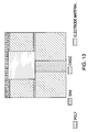
Referring to FIG. 10, there is shown a preferred basic topographic pattern 8 comprising a plane packed with interlocking hexagons. Hexagons are preferred because they pack a planar space uniformly and provide considerable surface area, but not so much surface area as to be difficult to etch. It is preferred that individual topographic features 10 be on the scale of about one order of magnitude smaller than the width or height of the electrode, give or take half an order of magnitude.
Note that the mask may be used as is, such as to etch a positive topographic pattern 8 a having hexagonal pits 10 a as already described in FIGS. 1 through 9, or the negative version 8b may be used to etch out the valleys 10 a between hexagonal pillars 10 b as can be seen in FIGS. 12 through 15. The steps of FIGS. 1 through 5 are identical for each method, therefore FIGS. 1 through 4 are not duplicated and FIG. 5 is exactly duplicated as FIG. 12 for convenient reference. Hence, FIG. 12 shows the transfer of the topographic pattern onto the hard mask, FIG. 13 shows the filling of the nitride hard mask pattern with silicon oxide and planarizing with chemical/mechanical polishing (CMP), FIG. 14 shows the resulting silicon oxide pattern after the silicon nitride hard mask is removed. It is in FIG. 14 that the reversal of the resist pattern occurs—what had been masked areas in FIG. 1 though 9 are now clear and what was clear is now masked. FIG. 15 finishes the transfer of the oxide mask pattern into the storage node conductive material.
FIG. 11 is a drawing derived from an actual scanning electron microscope image of a positive tone polymer film hexagonal pattern, such as in 8 a of FIG. 10, just prior to etching of the pattern into a semiconductor substrate.
A method of making the nanoscale topographic patterns shown in FIGS. 10 and 11 is by using a film of polystyrene-polybutadiene diblock copolymer as a starting material that self-assembles into a hexagonally packed array of polybutadiene (PB) cylinders embedded in a polystyrene (PS) matrix. The PB cylinders are made to orient normal to the plane of the film by, among other known means, spreading a drop of dilute polymer solution in toluene, or like solvent, onto the surface of a de-ionized water bath and allowing the toluene to evaporate. This leaves behind a film typically 100 to 200 nm thick, which may then be deposited upon the surface of the semiconductor. The PB cylinders are then removed by annealing and reaction with ozone, which reacts more rapidly with the PB than with the PS, thereby leaving behind a nanoscale thin film with hexagonally stacked holes typically about 13 nm in diameter, though by controlling the molecular weights of the copolymers one can control the hole size to range from about 2 to about 100 nanometers, such as from about 10 to about 50 nanometers, such as for example from about 10 to about 25 nanometers in diameter and spaced from about 2 to about 100 nanometers apart, such as from about 10 to about 50 nanometers apart, such as for example from about 10 to about 25 nanometers apart, which represent the typical ranges using any of the methods described herein.
A method of inverting the topographic pattern is to treat the film with a blocking stain, usually Osmium, OsO4, which selectively binds to the PB cylinders. This now causes the ozone to attack the PS component at a faster rate than PB, thereby leaving behind a pattern of hexagonally stacked dots instead of holes.
Another method of making topographic patterns is to use a polystyrene-polyisoprene diblock copolymer. This material is similar to the PS-PB copolymer described above, except that the polyisoprene (PI) component self-assembles into spheres instead of cylinders. Hence, there is no need to orient the PI component to the plane of the film. PS-PI films may also be treated with an Osmium stain to create an inverted pattern.
Another method of making the nanoscale topographic patterns of FIGS. 10 and 11 is by using a film of polystyrene-polymethylmethacrylate (PMMA) diblock copolymer as a starting material. The diblock copolymer film can be made to self-assemble into a hexagonally packed array of PMMA cylinders in a polystyrene matrix. The PMMA cylinders can be made to orient normal to the plane of the film by, among other known means, spin-coating a dilute polymer solution in toluene, or other solvent, onto the substrate and annealing the resulting film. The PMMA cylinders are then removed by exposure to electron-beam or ultraviolet radiation and dissolution in acetic acid or other effective solvent. The resulting nanoscale thin film typically has hexagonally packed holes about 20 nanometers in diameter. By controlling the molecular weights and relative ratios of the two polymer blocks, one can control the hole size range from about 2 nanometers up to about 100 nanometers, such as from about 10 to about 50 nanometers, such as from about 10 to about 25 nanometers, and the hole separations from about 2 nanometers up to about 100 nanometers, such as from about 10 to about 50 nanometers, such as from about 10 to about 25 nanometers.
Such methods for creating topographic patterns as described above are set forth in greater detail in Mansky et al., Nanolithographic Templates from Diblock Copolymer Thin Films, Applied Physics Letters, vol. 68, pp.2586-2588 (1996); and Park et al., Block Copolymer Lithography: Periodic Arrays of ˜1011Holes in 1 Square Centimeter, Science, vol. 276, May 30, pp. 1401-1404 (1997), the disclosures of both of which are incorporated by reference herein in their entirety.
Other suitable methods for creating and using topographic patterns may be found in Morkved et al., Science, v. 273, p. 931 (1998); Morkved et al., Applied Physics Letters, v. 64, p. 422 (1994); Mansky et al., Journal of Material Science, v. 30, p. 1937 (1995); and Li et al., Journal of the American Chemical Society, v. 118, p. 10982 (1996), the disclosures of all four of which are incorporated by reference herein in their entirety.
Alternatively, one may use technologies other than diblock copolymers to make the topographic patterns, such as providing films of inorganic crystals embedded in a coating layer. For example, it is known that SiGe films, when oxidized and then reduced with hydrogen, will undergo reduction of the Germanium and form nanoscale inorganic crystals of Ge embedded in a silicon oxide film, which acts as the coating layer. By selectively etching out the silicon oxide, an array of nanometer scale germanium islands remain on the substrate, thereby increasing surface area. Alternatively, the Germanium could be etched away, thereby leaving a silicon oxide plane pitted with craters where once germanium crystal once stood. The ranges of inorganic crystal diameters will typically be from about 2 to about 100 nanometers, such as from about 10 to about 50 nanometers, such as from about 10 to about 25 nanometers, and spaced from about 2 to about 100 nanometers, such as from about 10 to about 50 nanometers, such as from about 10 to about 25 nanometers apart. Generally the inorganic crystals will have a size distribution of not more than about 20 percent, such as not exceeding about 10 percent, such as for example not more than 5 percent.
In yet another embodiment, nanoscopic particles of Cobalt and the like may be deposited in a liquid solution to form the mask.
It is to be understood that all physical quantities disclosed herein, unless explicitly indicated otherwise, are not to be construed as exactly equal to the quantity disclosed, but rather about equal to the quantity disclosed. Further, the mere absence of a qualifier such as “about, or the like, is not to be construed as an explicit indication that any such disclosed physical quantity is an exact quantity, irrespective of whether such qualifiers are used with respect to any other physical quantities disclosed herein.
While preferred embodiments have been shown and described, various modifications and substitutions may be made thereto without departing from the spirit and scope of the invention. Accordingly, it is to be understood that the present invention has been described by way of illustration only, and such illustrations and embodiments as have been disclosed herein are not to be construed as limiting to the claims.
Claims (18)
1. A method for forming nanoscale features, comprising:
providing a substrate;
disposing a masking film over the substrate;
disposing a self-forming nanoscale mesh layer over the masking film;
patterning the masking film through the nanoscale mesh for forming a nanoscale mesh mask in a first portion of the masking film, re n portions of said masking film being only partially patterned; and
etching the substrate through said first portion of the mask for forming nanoscale features.
2. The method of claim 1 wherein the step of etching the substrate through the mask for forming nanoscale features includes forming a plurality of pillars in the substrate defined by the mesh mask.
3. The method of claim 2 wherein the substrate comprises a first conductor add said method further comprises:
disposing a layer of dielectric on the pillars;
disposing a second conductor on the layer of dielectric for forming a capacitor, a first electrode of the capacitor comprising the first conductor and a second electrode of the capacitor comprising the second conductor.
4. The method of claim 1 wherein said step of disposing said self-forming nanoscale mesh polymer layer comprises:
providing a copolymer film comprising a plurality of polymer blocks;
selectively removing one of said polymer blocks so as to create a topographic pattern.
5. The method of claim 4 wherein said copolymer is a diblock copolymer.
6. The method of claim 5 wherein said copolymer comprises a first component selected from the group consisting of polymethylmethacrylate, polybutadiene, and polyisoprene, and a second component comprised of polystyrene.
7. The method of claim 6 further comprising removing said first component with ultraviolet radiation and dissolution in a solvent.
8. The method of claim 6 further comprising removing said first component with electron-beam radiation and dissolution in a solvent.
9. The method of claim 6 further comprising removing said fist component by annealing and reaction with ozone.
10. The method of claim 4 wherein said copolymer is a triblock copolymer.
11. The method of claim 1 wherein said step of disposing said self-forming nanoscale mesh polymer layer comprises:
providing a SiGe film;
oxidizing and reducing said SiGe film so as to create germanium crystals in a silicon oxide film; and
selectively removing one of said germanium crystals or silicon oxide so as to create a topographic pattern.
12. The method of claim 1 wherein said nanoscale features are from about 2 to about 100 nanometers wide and spaced from about 2 to about 100 nanometers apart.
13. The method of claim 1 wherein said nanoscale features are from about 10 to 50 nanometers wide and spaced about 10 to about 50 nanometers apart.
14. The method of claim 1 wherein said step of disposing said self-forming nanoscale mesh polymer layer comprises immersing the substrate in a solution from which said polymer layer deposits on said making film.
15. The method of claim 14 wherein said polymer floats on an upper surface of said solution
16. The method of claim 1 wherein said nanoscale mesh comprises a plurality of hexagon shapes.
17. The method of claim 16 wherein said plurality of hexagon shapes are arranged in an interlocking pattern.
18. The method of claim 1 wherein said first portion of said masking film is thinner than said remaining portions of said masking film.
Priority Applications (1)
| Application Number | Priority Date | Filing Date | Title |
|---|---|---|---|
| US10/008,092 US6506660B2 (en) | 2000-11-15 | 2001-11-13 | Semiconductor with nanoscale features |
Applications Claiming Priority (2)
| Application Number | Priority Date | Filing Date | Title |
|---|---|---|---|
| US09/713,766 US6358813B1 (en) | 2000-11-15 | 2000-11-15 | Method for increasing the capacitance of a semiconductor capacitors |
| US10/008,092 US6506660B2 (en) | 2000-11-15 | 2001-11-13 | Semiconductor with nanoscale features |
Related Parent Applications (1)
| Application Number | Title | Priority Date | Filing Date |
|---|---|---|---|
| US09/713,766 Division US6358813B1 (en) | 2000-11-15 | 2000-11-15 | Method for increasing the capacitance of a semiconductor capacitors |
Publications (2)
| Publication Number | Publication Date |
|---|---|
| US20020058394A1 US20020058394A1 (en) | 2002-05-16 |
| US6506660B2 true US6506660B2 (en) | 2003-01-14 |
Family
ID=24867453
Family Applications (2)
| Application Number | Title | Priority Date | Filing Date |
|---|---|---|---|
| US09/713,766 Expired - Lifetime US6358813B1 (en) | 2000-11-15 | 2000-11-15 | Method for increasing the capacitance of a semiconductor capacitors |
| US10/008,092 Expired - Fee Related US6506660B2 (en) | 2000-11-15 | 2001-11-13 | Semiconductor with nanoscale features |
Family Applications Before (1)
| Application Number | Title | Priority Date | Filing Date |
|---|---|---|---|
| US09/713,766 Expired - Lifetime US6358813B1 (en) | 2000-11-15 | 2000-11-15 | Method for increasing the capacitance of a semiconductor capacitors |
Country Status (1)
| Country | Link |
|---|---|
| US (2) | US6358813B1 (en) |
Cited By (33)
| Publication number | Priority date | Publication date | Assignee | Title |
|---|---|---|---|---|
| US20050167838A1 (en) * | 2004-01-30 | 2005-08-04 | International Business Machines Corporation | Device and methodology for reducing effective dielectric constant in semiconductor devices |
| US7071047B1 (en) | 2005-01-28 | 2006-07-04 | International Business Machines Corporation | Method of forming buried isolation regions in semiconductor substrates and semiconductor devices with buried isolation regions |
| US20060276043A1 (en) * | 2003-03-21 | 2006-12-07 | Johnson Mark A L | Method and systems for single- or multi-period edge definition lithography |
| US20070212795A1 (en) * | 2006-03-07 | 2007-09-13 | Milkove Keith R | Device and method for improving interface adhesion in thin film structures |
| US20070249127A1 (en) * | 2006-04-24 | 2007-10-25 | Freescale Semiconductor, Inc. | Electronic device including a semiconductor layer and a sidewall spacer and a process of forming the same |
| US20070246793A1 (en) * | 2006-04-24 | 2007-10-25 | Freescale Semiconductor, Inc. | Electronic device including a semiconductor layer and another layer adjacent to an opening within the semiconductor layer and a process of forming the same |
| US20070249160A1 (en) * | 2006-04-24 | 2007-10-25 | Freescale Semiconductor, Inc. | Process of forming an electronic device including a layer formed using an inductively coupled plasma |
| US20070264839A1 (en) * | 2006-05-12 | 2007-11-15 | Freescale Semiconductor, Inc. | Process of forming electronic device including a densified nitride layer adjacent to an opening within a semiconductor layer |
| US20080026541A1 (en) * | 2006-07-26 | 2008-01-31 | International Business Machines Corporation | Air-gap interconnect structures with selective cap |
| US20080157269A1 (en) * | 2007-01-03 | 2008-07-03 | International Business Machines Corporation | Reversible electric fuse and antifuse structures for semiconductor devices |
| US20080217292A1 (en) * | 2007-03-06 | 2008-09-11 | Micron Technology, Inc. | Registered structure formation via the application of directed thermal energy to diblock copolymer films |
| US20080257187A1 (en) * | 2007-04-18 | 2008-10-23 | Micron Technology, Inc. | Methods of forming a stamp, methods of patterning a substrate, and a stamp and a patterning system for same |
| US20080274413A1 (en) * | 2007-03-22 | 2008-11-06 | Micron Technology, Inc. | Sub-10 nm line features via rapid graphoepitaxial self-assembly of amphiphilic monolayers |
| US20080286659A1 (en) * | 2007-04-20 | 2008-11-20 | Micron Technology, Inc. | Extensions of Self-Assembled Structures to Increased Dimensions via a "Bootstrap" Self-Templating Method |
| US20080311347A1 (en) * | 2007-06-12 | 2008-12-18 | Millward Dan B | Alternating Self-Assembling Morphologies of Diblock Copolymers Controlled by Variations in Surfaces |
| US20080315270A1 (en) * | 2007-06-21 | 2008-12-25 | Micron Technology, Inc. | Multilayer antireflection coatings, structures and devices including the same and methods of making the same |
| US20080318005A1 (en) * | 2007-06-19 | 2008-12-25 | Millward Dan B | Crosslinkable Graft Polymer Non-Preferentially Wetted by Polystyrene and Polyethylene Oxide |
| US20090001045A1 (en) * | 2007-06-27 | 2009-01-01 | International Business Machines Corporation | Methods of patterning self-assembly nano-structure and forming porous dielectric |
| US20090200646A1 (en) * | 2008-02-13 | 2009-08-13 | Millward Dan B | One-Dimensional Arrays of Block Copolymer Cylinders and Applications Thereof |
| US20090240001A1 (en) * | 2008-03-21 | 2009-09-24 | Jennifer Kahl Regner | Methods of Improving Long Range Order in Self-Assembly of Block Copolymer Films with Ionic Liquids |
| US20090236309A1 (en) * | 2008-03-21 | 2009-09-24 | Millward Dan B | Thermal Anneal of Block Copolymer Films with Top Interface Constrained to Wet Both Blocks with Equal Preference |
| US20090242892A1 (en) * | 1994-06-09 | 2009-10-01 | Semiconductor Energy Laboratory Co., Ltd. | Semiconductor device and method for forming the same |
| US20090263628A1 (en) * | 2008-04-21 | 2009-10-22 | Millward Dan B | Multi-Layer Method for Formation of Registered Arrays of Cylindrical Pores in Polymer Films |
| US20090274887A1 (en) * | 2008-05-02 | 2009-11-05 | Millward Dan B | Graphoepitaxial Self-Assembly of Arrays of Downward Facing Half-Cylinders |
| US20100102415A1 (en) * | 2008-10-28 | 2010-04-29 | Micron Technology, Inc. | Methods for selective permeation of self-assembled block copolymers with metal oxides, methods for forming metal oxide structures, and semiconductor structures including same |
| US20100316849A1 (en) * | 2008-02-05 | 2010-12-16 | Millward Dan B | Method to Produce Nanometer-Sized Features with Directed Assembly of Block Copolymers |
| US8394483B2 (en) | 2007-01-24 | 2013-03-12 | Micron Technology, Inc. | Two-dimensional arrays of holes with sub-lithographic diameters formed by block copolymer self-assembly |
| US8450418B2 (en) | 2010-08-20 | 2013-05-28 | Micron Technology, Inc. | Methods of forming block copolymers, and block copolymer compositions |
| US8900963B2 (en) | 2011-11-02 | 2014-12-02 | Micron Technology, Inc. | Methods of forming semiconductor device structures, and related structures |
| US9087699B2 (en) | 2012-10-05 | 2015-07-21 | Micron Technology, Inc. | Methods of forming an array of openings in a substrate, and related methods of forming a semiconductor device structure |
| US9177795B2 (en) | 2013-09-27 | 2015-11-03 | Micron Technology, Inc. | Methods of forming nanostructures including metal oxides |
| US9229328B2 (en) | 2013-05-02 | 2016-01-05 | Micron Technology, Inc. | Methods of forming semiconductor device structures, and related semiconductor device structures |
| US11120941B2 (en) * | 2018-01-24 | 2021-09-14 | Semiconductor Components Industries, Llc | Methods of forming capacitors |
Families Citing this family (14)
| Publication number | Priority date | Publication date | Assignee | Title |
|---|---|---|---|---|
| US20030135552A1 (en) * | 2002-01-14 | 2003-07-17 | Blackstock Michael A. | Method for discovering and discriminating devices on local collaborative networks to facilitate collaboration among users |
| US7613772B2 (en) * | 2002-07-25 | 2009-11-03 | Colligo Networks, Inc. | Method for context based discovery and filtering of portable collaborative networks |
| US7045851B2 (en) * | 2003-06-20 | 2006-05-16 | International Business Machines Corporation | Nonvolatile memory device using semiconductor nanocrystals and method of forming same |
| US20090222537A1 (en) * | 2003-12-04 | 2009-09-03 | Colligo Newworks, Inc., A Canadian Corporation | System And Method For Interactive Instant Networking |
| DE102004033825B4 (en) * | 2004-07-13 | 2009-05-14 | Infineon Technologies Ag | Method for producing a capacitor arrangement and associated capacitor arrangement |
| KR100842903B1 (en) * | 2005-06-10 | 2008-07-02 | 주식회사 하이닉스반도체 | Phase change RAM device and method of manufacturing the same |
| KR100668846B1 (en) * | 2005-06-10 | 2007-01-16 | 주식회사 하이닉스반도체 | Method of manufacturing phase change RAM device |
| US7482270B2 (en) * | 2006-12-05 | 2009-01-27 | International Business Machines Corporation | Fully and uniformly silicided gate structure and method for forming same |
| CN103094095B (en) * | 2011-10-28 | 2015-10-21 | 中芯国际集成电路制造(北京)有限公司 | Manufacture the method for semiconductor device |
| US9306164B1 (en) | 2015-01-30 | 2016-04-05 | International Business Machines Corporation | Electrode pair fabrication using directed self assembly of diblock copolymers |
| US10325920B2 (en) * | 2016-05-13 | 2019-06-18 | Toshiba Memory Corporation | Method for manufacturing semiconductor device |
| US10090378B1 (en) | 2017-03-17 | 2018-10-02 | International Business Machines Corporation | Efficient metal-insulator-metal capacitor |
| US11121209B2 (en) | 2017-03-27 | 2021-09-14 | International Business Machines Corporation | Surface area enhancement for stacked metal-insulator-metal (MIM) capacitor |
| CN109427687B (en) | 2017-09-04 | 2021-02-09 | 联华电子股份有限公司 | Method for manufacturing semiconductor element |
Citations (3)
| Publication number | Priority date | Publication date | Assignee | Title |
|---|---|---|---|---|
| US5757612A (en) | 1996-04-23 | 1998-05-26 | International Business Machines Corporation | Structure and fabrication method for non-planar memory elements |
| US5772905A (en) * | 1995-11-15 | 1998-06-30 | Regents Of The University Of Minnesota | Nanoimprint lithography |
| US5922214A (en) * | 1997-01-17 | 1999-07-13 | Wayne State University | Nanometer scale fabrication method to produce thin film nanostructures |
-
2000
- 2000-11-15 US US09/713,766 patent/US6358813B1/en not_active Expired - Lifetime
-
2001
- 2001-11-13 US US10/008,092 patent/US6506660B2/en not_active Expired - Fee Related
Patent Citations (3)
| Publication number | Priority date | Publication date | Assignee | Title |
|---|---|---|---|---|
| US5772905A (en) * | 1995-11-15 | 1998-06-30 | Regents Of The University Of Minnesota | Nanoimprint lithography |
| US5757612A (en) | 1996-04-23 | 1998-05-26 | International Business Machines Corporation | Structure and fabrication method for non-planar memory elements |
| US5922214A (en) * | 1997-01-17 | 1999-07-13 | Wayne State University | Nanometer scale fabrication method to produce thin film nanostructures |
Non-Patent Citations (8)
| Title |
|---|
| Hiroshi Ikeda, Michiei Nakamura, Nobuyuki Ise, Naomi Oguma, Asao Nakamura, Tuskasa Ideda, Fujio Toda, and Akihiko Ueno; "Fluorescent Cyclodextrins for Molecule Sensing: Fluorescent Properties, NMR Characterization, and Inclusion Phenoma of N-Dansylleucine-Modified Cyclodextrins," Journal of the American Chemical Society, vol. 118, No. 45, Nov. 13, 1996; p. 10982. |
| Miri Park, Christopher Harrison, Paul M. Chaikin, Richard A. Register, and Douglas H. Adamson; "Block Copolymer Lithography: Periodic Arrays of ~ 10 11 Holes in 1 Square Centimeter," Science, vol. 276, No. 5317, May 30, 1997; pp. 1401-1404. |
| Miri Park, Christopher Harrison, Paul M. Chaikin, Richard A. Register, and Douglas H. Adamson; "Block Copolymer Lithography: Periodic Arrays of ˜ 10 11 Holes in 1 Square Centimeter," Science, vol. 276, No. 5317, May 30, 1997; pp. 1401-1404. |
| P. Mansky, C.K. Harrison, and P.M. Chakin; "Nanolithographic Templates from Diblock Copolymers Thin Films," Applied Physics Letters, vol. 68, No. 18, Apr. 29, 1996, pp. 2586-2588. |
| P. Mansky, P. Chaikin, and E. L. Thomas; "Monolayer Films of Diblock Copolymer Microdomains for Nanolithographic Applications," Journal of Material Science, vol. 30, No. 8, Apr. 15, 1995; pp. 1987-1992. |
| T. L. Morkved, M. Lu, A.M. Urbas, E.E. Ehrichs, H.M. Jaeger, P. Mansky, and T.P. Russel; "Local Control of Microdomain Orientation in Diblock Copolymer Thin Films with Electric Fields," Science, vol. 273, No. 5277, Aug. 16, 1996; pp. 931-933. |
| T.L. Morkved, P. Wiltzius, H.M. Jaeger, D.G. Grier, and T.A. Witten; "Mesoscopic Self-Assembly of Gold Islands on Diblock-Copolymer Films," Applied Physics Letter vol. 64, No. 4, Jan. 24, 1994; pp. 422-424. |
| Z. Ki, W. Zhao, Y. Liu, M. H. Rafailovich, and J. Sokolov; "Self-Ordering of Diblock Copolymers from Solution," Journal of the American Chemical Society, vol. 118, No. 44, Nov. 6, 1996; pp. 10892-10893. |
Cited By (100)
| Publication number | Priority date | Publication date | Assignee | Title |
|---|---|---|---|---|
| US20090242892A1 (en) * | 1994-06-09 | 2009-10-01 | Semiconductor Energy Laboratory Co., Ltd. | Semiconductor device and method for forming the same |
| US8330165B2 (en) | 1994-06-09 | 2012-12-11 | Semiconductor Energy Laboratory Co., Ltd. | Semiconductor device and method for forming the same |
| US20060276043A1 (en) * | 2003-03-21 | 2006-12-07 | Johnson Mark A L | Method and systems for single- or multi-period edge definition lithography |
| US20080254630A1 (en) * | 2004-01-30 | 2008-10-16 | International Business Machines Corporation | Device and methodology for reducing effective dielectric constant in semiconductor devices |
| US20110111590A1 (en) * | 2004-01-30 | 2011-05-12 | International Business Machines Corporation | Device and methodology for reducing effective dielectric constant in semiconductor devices |
| CN100428422C (en) * | 2004-01-30 | 2008-10-22 | 国际商业机器公司 | Device and methodology for reducing effective dielectric constant in semiconductor devices |
| US20050167838A1 (en) * | 2004-01-30 | 2005-08-04 | International Business Machines Corporation | Device and methodology for reducing effective dielectric constant in semiconductor devices |
| US7592685B2 (en) | 2004-01-30 | 2009-09-22 | International Business Machines Corporation | Device and methodology for reducing effective dielectric constant in semiconductor devices |
| US8129286B2 (en) | 2004-01-30 | 2012-03-06 | International Business Machines Corporation | Reducing effective dielectric constant in semiconductor devices |
| US8343868B2 (en) * | 2004-01-30 | 2013-01-01 | International Business Machines Corporation | Device and methodology for reducing effective dielectric constant in semiconductor devices |
| US20080038923A1 (en) * | 2004-01-30 | 2008-02-14 | International Business Machines Corporation | Device and methodology for reducing effective dielectric constant in semiconductor devices |
| US20080038915A1 (en) * | 2004-01-30 | 2008-02-14 | International Business Machines Corporation | Device and methodology for reducing effective dielectric constant in semiconductor devices |
| US7892940B2 (en) * | 2004-01-30 | 2011-02-22 | International Business Machines Corporation | Device and methodology for reducing effective dielectric constant in semiconductor devices |
| US7405147B2 (en) * | 2004-01-30 | 2008-07-29 | International Business Machines Corporation | Device and methodology for reducing effective dielectric constant in semiconductor devices |
| US20060172479A1 (en) * | 2005-01-28 | 2006-08-03 | International Business Machines Corporation | Method of forming buried isolation regions in semiconductor substrates and semiconductor devices with buried isolation regions |
| US7352030B2 (en) | 2005-01-28 | 2008-04-01 | International Business Machines Corporation | Semiconductor devices with buried isolation regions |
| US7071047B1 (en) | 2005-01-28 | 2006-07-04 | International Business Machines Corporation | Method of forming buried isolation regions in semiconductor substrates and semiconductor devices with buried isolation regions |
| US20070212795A1 (en) * | 2006-03-07 | 2007-09-13 | Milkove Keith R | Device and method for improving interface adhesion in thin film structures |
| US7488661B2 (en) | 2006-03-07 | 2009-02-10 | International Business Machines Corporation | Device and method for improving interface adhesion in thin film structures |
| US7491622B2 (en) | 2006-04-24 | 2009-02-17 | Freescale Semiconductor, Inc. | Process of forming an electronic device including a layer formed using an inductively coupled plasma |
| US7670895B2 (en) | 2006-04-24 | 2010-03-02 | Freescale Semiconductor, Inc | Process of forming an electronic device including a semiconductor layer and another layer adjacent to an opening within the semiconductor layer |
| US20070246793A1 (en) * | 2006-04-24 | 2007-10-25 | Freescale Semiconductor, Inc. | Electronic device including a semiconductor layer and another layer adjacent to an opening within the semiconductor layer and a process of forming the same |
| US20070249160A1 (en) * | 2006-04-24 | 2007-10-25 | Freescale Semiconductor, Inc. | Process of forming an electronic device including a layer formed using an inductively coupled plasma |
| US20070249127A1 (en) * | 2006-04-24 | 2007-10-25 | Freescale Semiconductor, Inc. | Electronic device including a semiconductor layer and a sidewall spacer and a process of forming the same |
| US20070264839A1 (en) * | 2006-05-12 | 2007-11-15 | Freescale Semiconductor, Inc. | Process of forming electronic device including a densified nitride layer adjacent to an opening within a semiconductor layer |
| US7528078B2 (en) | 2006-05-12 | 2009-05-05 | Freescale Semiconductor, Inc. | Process of forming electronic device including a densified nitride layer adjacent to an opening within a semiconductor layer |
| US20080026541A1 (en) * | 2006-07-26 | 2008-01-31 | International Business Machines Corporation | Air-gap interconnect structures with selective cap |
| US7557424B2 (en) | 2007-01-03 | 2009-07-07 | International Business Machines Corporation | Reversible electric fuse and antifuse structures for semiconductor devices |
| US20080157269A1 (en) * | 2007-01-03 | 2008-07-03 | International Business Machines Corporation | Reversible electric fuse and antifuse structures for semiconductor devices |
| US8394483B2 (en) | 2007-01-24 | 2013-03-12 | Micron Technology, Inc. | Two-dimensional arrays of holes with sub-lithographic diameters formed by block copolymer self-assembly |
| US8512846B2 (en) | 2007-01-24 | 2013-08-20 | Micron Technology, Inc. | Two-dimensional arrays of holes with sub-lithographic diameters formed by block copolymer self-assembly |
| US8409449B2 (en) | 2007-03-06 | 2013-04-02 | Micron Technology, Inc. | Registered structure formation via the application of directed thermal energy to diblock copolymer films |
| US20080217292A1 (en) * | 2007-03-06 | 2008-09-11 | Micron Technology, Inc. | Registered structure formation via the application of directed thermal energy to diblock copolymer films |
| US8083953B2 (en) | 2007-03-06 | 2011-12-27 | Micron Technology, Inc. | Registered structure formation via the application of directed thermal energy to diblock copolymer films |
| US8753738B2 (en) | 2007-03-06 | 2014-06-17 | Micron Technology, Inc. | Registered structure formation via the application of directed thermal energy to diblock copolymer films |
| US8784974B2 (en) | 2007-03-22 | 2014-07-22 | Micron Technology, Inc. | Sub-10 NM line features via rapid graphoepitaxial self-assembly of amphiphilic monolayers |
| US8801894B2 (en) | 2007-03-22 | 2014-08-12 | Micron Technology, Inc. | Sub-10 NM line features via rapid graphoepitaxial self-assembly of amphiphilic monolayers |
| US8557128B2 (en) | 2007-03-22 | 2013-10-15 | Micron Technology, Inc. | Sub-10 nm line features via rapid graphoepitaxial self-assembly of amphiphilic monolayers |
| US20100163180A1 (en) * | 2007-03-22 | 2010-07-01 | Millward Dan B | Sub-10 NM Line Features Via Rapid Graphoepitaxial Self-Assembly of Amphiphilic Monolayers |
| US20080274413A1 (en) * | 2007-03-22 | 2008-11-06 | Micron Technology, Inc. | Sub-10 nm line features via rapid graphoepitaxial self-assembly of amphiphilic monolayers |
| US20110232515A1 (en) * | 2007-04-18 | 2011-09-29 | Micron Technology, Inc. | Methods of forming a stamp, a stamp and a patterning system |
| US8956713B2 (en) | 2007-04-18 | 2015-02-17 | Micron Technology, Inc. | Methods of forming a stamp and a stamp |
| US9768021B2 (en) | 2007-04-18 | 2017-09-19 | Micron Technology, Inc. | Methods of forming semiconductor device structures including metal oxide structures |
| US7959975B2 (en) | 2007-04-18 | 2011-06-14 | Micron Technology, Inc. | Methods of patterning a substrate |
| US20080257187A1 (en) * | 2007-04-18 | 2008-10-23 | Micron Technology, Inc. | Methods of forming a stamp, methods of patterning a substrate, and a stamp and a patterning system for same |
| US9276059B2 (en) | 2007-04-18 | 2016-03-01 | Micron Technology, Inc. | Semiconductor device structures including metal oxide structures |
| US8372295B2 (en) | 2007-04-20 | 2013-02-12 | Micron Technology, Inc. | Extensions of self-assembled structures to increased dimensions via a “bootstrap” self-templating method |
| US20080286659A1 (en) * | 2007-04-20 | 2008-11-20 | Micron Technology, Inc. | Extensions of Self-Assembled Structures to Increased Dimensions via a "Bootstrap" Self-Templating Method |
| US9142420B2 (en) | 2007-04-20 | 2015-09-22 | Micron Technology, Inc. | Extensions of self-assembled structures to increased dimensions via a “bootstrap” self-templating method |
| US20080311347A1 (en) * | 2007-06-12 | 2008-12-18 | Millward Dan B | Alternating Self-Assembling Morphologies of Diblock Copolymers Controlled by Variations in Surfaces |
| US9257256B2 (en) | 2007-06-12 | 2016-02-09 | Micron Technology, Inc. | Templates including self-assembled block copolymer films |
| US20100279062A1 (en) * | 2007-06-12 | 2010-11-04 | Millward Dan B | Alternating Self-Assembling Morphologies of Diblock Copolymers Controlled by Variations in Surfaces |
| US8609221B2 (en) | 2007-06-12 | 2013-12-17 | Micron Technology, Inc. | Alternating self-assembling morphologies of diblock copolymers controlled by variations in surfaces |
| US8404124B2 (en) | 2007-06-12 | 2013-03-26 | Micron Technology, Inc. | Alternating self-assembling morphologies of diblock copolymers controlled by variations in surfaces |
| US8785559B2 (en) | 2007-06-19 | 2014-07-22 | Micron Technology, Inc. | Crosslinkable graft polymer non-preferentially wetted by polystyrene and polyethylene oxide |
| US20080318005A1 (en) * | 2007-06-19 | 2008-12-25 | Millward Dan B | Crosslinkable Graft Polymer Non-Preferentially Wetted by Polystyrene and Polyethylene Oxide |
| US8513359B2 (en) | 2007-06-19 | 2013-08-20 | Micron Technology, Inc. | Crosslinkable graft polymer non preferentially wetted by polystyrene and polyethylene oxide |
| US8080615B2 (en) | 2007-06-19 | 2011-12-20 | Micron Technology, Inc. | Crosslinkable graft polymer non-preferentially wetted by polystyrene and polyethylene oxide |
| US8445592B2 (en) | 2007-06-19 | 2013-05-21 | Micron Technology, Inc. | Crosslinkable graft polymer non-preferentially wetted by polystyrene and polyethylene oxide |
| US20080315270A1 (en) * | 2007-06-21 | 2008-12-25 | Micron Technology, Inc. | Multilayer antireflection coatings, structures and devices including the same and methods of making the same |
| US8294139B2 (en) | 2007-06-21 | 2012-10-23 | Micron Technology, Inc. | Multilayer antireflection coatings, structures and devices including the same and methods of making the same |
| US8551808B2 (en) | 2007-06-21 | 2013-10-08 | Micron Technology, Inc. | Methods of patterning a substrate including multilayer antireflection coatings |
| US20090001045A1 (en) * | 2007-06-27 | 2009-01-01 | International Business Machines Corporation | Methods of patterning self-assembly nano-structure and forming porous dielectric |
| US8999492B2 (en) | 2008-02-05 | 2015-04-07 | Micron Technology, Inc. | Method to produce nanometer-sized features with directed assembly of block copolymers |
| US11560009B2 (en) | 2008-02-05 | 2023-01-24 | Micron Technology, Inc. | Stamps including a self-assembled block copolymer material, and related methods |
| US10828924B2 (en) | 2008-02-05 | 2020-11-10 | Micron Technology, Inc. | Methods of forming a self-assembled block copolymer material |
| US10005308B2 (en) | 2008-02-05 | 2018-06-26 | Micron Technology, Inc. | Stamps and methods of forming a pattern on a substrate |
| US20100316849A1 (en) * | 2008-02-05 | 2010-12-16 | Millward Dan B | Method to Produce Nanometer-Sized Features with Directed Assembly of Block Copolymers |
| US8642157B2 (en) | 2008-02-13 | 2014-02-04 | Micron Technology, Inc. | One-dimensional arrays of block copolymer cylinders and applications thereof |
| US8101261B2 (en) | 2008-02-13 | 2012-01-24 | Micron Technology, Inc. | One-dimensional arrays of block copolymer cylinders and applications thereof |
| US20090200646A1 (en) * | 2008-02-13 | 2009-08-13 | Millward Dan B | One-Dimensional Arrays of Block Copolymer Cylinders and Applications Thereof |
| US20090236309A1 (en) * | 2008-03-21 | 2009-09-24 | Millward Dan B | Thermal Anneal of Block Copolymer Films with Top Interface Constrained to Wet Both Blocks with Equal Preference |
| US11282741B2 (en) | 2008-03-21 | 2022-03-22 | Micron Technology, Inc. | Methods of forming a semiconductor device using block copolymer materials |
| US8641914B2 (en) | 2008-03-21 | 2014-02-04 | Micron Technology, Inc. | Methods of improving long range order in self-assembly of block copolymer films with ionic liquids |
| US8426313B2 (en) | 2008-03-21 | 2013-04-23 | Micron Technology, Inc. | Thermal anneal of block copolymer films with top interface constrained to wet both blocks with equal preference |
| US10153200B2 (en) | 2008-03-21 | 2018-12-11 | Micron Technology, Inc. | Methods of forming a nanostructured polymer material including block copolymer materials |
| US20090240001A1 (en) * | 2008-03-21 | 2009-09-24 | Jennifer Kahl Regner | Methods of Improving Long Range Order in Self-Assembly of Block Copolymer Films with Ionic Liquids |
| US9682857B2 (en) | 2008-03-21 | 2017-06-20 | Micron Technology, Inc. | Methods of improving long range order in self-assembly of block copolymer films with ionic liquids and materials produced therefrom |
| US9315609B2 (en) | 2008-03-21 | 2016-04-19 | Micron Technology, Inc. | Thermal anneal of block copolymer films with top interface constrained to wet both blocks with equal preference |
| US8425982B2 (en) | 2008-03-21 | 2013-04-23 | Micron Technology, Inc. | Methods of improving long range order in self-assembly of block copolymer films with ionic liquids |
| US8633112B2 (en) | 2008-03-21 | 2014-01-21 | Micron Technology, Inc. | Thermal anneal of block copolymer films with top interface constrained to wet both blocks with equal preference |
| US8455082B2 (en) | 2008-04-21 | 2013-06-04 | Micron Technology, Inc. | Polymer materials for formation of registered arrays of cylindrical pores |
| US8114300B2 (en) * | 2008-04-21 | 2012-02-14 | Micron Technology, Inc. | Multi-layer method for formation of registered arrays of cylindrical pores in polymer films |
| US20090263628A1 (en) * | 2008-04-21 | 2009-10-22 | Millward Dan B | Multi-Layer Method for Formation of Registered Arrays of Cylindrical Pores in Polymer Films |
| US8114301B2 (en) | 2008-05-02 | 2012-02-14 | Micron Technology, Inc. | Graphoepitaxial self-assembly of arrays of downward facing half-cylinders |
| US20090274887A1 (en) * | 2008-05-02 | 2009-11-05 | Millward Dan B | Graphoepitaxial Self-Assembly of Arrays of Downward Facing Half-Cylinders |
| US8518275B2 (en) | 2008-05-02 | 2013-08-27 | Micron Technology, Inc. | Graphoepitaxial self-assembly of arrays of downward facing half-cylinders |
| US8993088B2 (en) | 2008-05-02 | 2015-03-31 | Micron Technology, Inc. | Polymeric materials in self-assembled arrays and semiconductor structures comprising polymeric materials |
| US20100102415A1 (en) * | 2008-10-28 | 2010-04-29 | Micron Technology, Inc. | Methods for selective permeation of self-assembled block copolymers with metal oxides, methods for forming metal oxide structures, and semiconductor structures including same |
| US8669645B2 (en) | 2008-10-28 | 2014-03-11 | Micron Technology, Inc. | Semiconductor structures including polymer material permeated with metal oxide |
| US8097175B2 (en) | 2008-10-28 | 2012-01-17 | Micron Technology, Inc. | Method for selectively permeating a self-assembled block copolymer, method for forming metal oxide structures, method for forming a metal oxide pattern, and method for patterning a semiconductor structure |
| US8450418B2 (en) | 2010-08-20 | 2013-05-28 | Micron Technology, Inc. | Methods of forming block copolymers, and block copolymer compositions |
| US9431605B2 (en) | 2011-11-02 | 2016-08-30 | Micron Technology, Inc. | Methods of forming semiconductor device structures |
| US8900963B2 (en) | 2011-11-02 | 2014-12-02 | Micron Technology, Inc. | Methods of forming semiconductor device structures, and related structures |
| US9087699B2 (en) | 2012-10-05 | 2015-07-21 | Micron Technology, Inc. | Methods of forming an array of openings in a substrate, and related methods of forming a semiconductor device structure |
| US9229328B2 (en) | 2013-05-02 | 2016-01-05 | Micron Technology, Inc. | Methods of forming semiconductor device structures, and related semiconductor device structures |
| US9177795B2 (en) | 2013-09-27 | 2015-11-03 | Micron Technology, Inc. | Methods of forming nanostructures including metal oxides |
| US10049874B2 (en) | 2013-09-27 | 2018-08-14 | Micron Technology, Inc. | Self-assembled nanostructures including metal oxides and semiconductor structures comprised thereof |
| US11532477B2 (en) | 2013-09-27 | 2022-12-20 | Micron Technology, Inc. | Self-assembled nanostructures including metal oxides and semiconductor structures comprised thereof |
| US11120941B2 (en) * | 2018-01-24 | 2021-09-14 | Semiconductor Components Industries, Llc | Methods of forming capacitors |
Also Published As
| Publication number | Publication date |
|---|---|
| US20020058394A1 (en) | 2002-05-16 |
| US6358813B1 (en) | 2002-03-19 |
Similar Documents
| Publication | Publication Date | Title |
|---|---|---|
| US6506660B2 (en) | Semiconductor with nanoscale features | |
| TW413846B (en) | Method for fabricating semiconductor device | |
| US9595387B2 (en) | High aspect ratio openings | |
| TWI360161B (en) | Pitch multiplication using self-assembling materia | |
| US7811940B2 (en) | Topography directed patterning | |
| US8114573B2 (en) | Topography based patterning | |
| US9035416B2 (en) | Efficient pitch multiplication process | |
| US5766968A (en) | Micro mask comprising agglomerated material | |
| US9087699B2 (en) | Methods of forming an array of openings in a substrate, and related methods of forming a semiconductor device structure | |
| US8748318B2 (en) | Methods of forming patterns in semiconductor constructions, methods of forming container capacitors, and methods of forming reticles configured for imprint lithography | |
| TW564515B (en) | Method for forming a storage node of a capacitor | |
| US20050179076A1 (en) | Method of forming DRAM capactiors with protected outside crown surface for more robust structures | |
| US5913118A (en) | Method of manufacturing trench DRAM cells with self-aligned field plate | |
| KR100376001B1 (en) | Polysilicon / Polyside Etching Method for Fine Gate Stacking | |
| Torii et al. | Process and properties of Pt/Pb (Zr, Ti) O3/Pt integrated ferroelectric capacitors | |
| US20090170322A1 (en) | Method for Manufacturing Semiconductor Device Including Vertical Transistor | |
| KR19990041068A (en) | HSS capacitor formation method to prevent bridge of capacitor lower electrode | |
| US6326276B1 (en) | Method for forming a capacitor in dram | |
| KR20010005040A (en) | Method of fabricating storage node of capacitor in semiconductor device | |
| KR20010001963A (en) | Method of forming a storage node in a semiconductor device | |
| KR20060030551A (en) | Forming method of bottom electrode in semiconductor device | |
| TW200814164A (en) | Method for fabricating bottom electrode of capacitor | |
| KR20050106925A (en) | Fabricating method of semiconductor device including meta stable polysilicon monitor pattern |
Legal Events
| Date | Code | Title | Description |
|---|---|---|---|
| FEPP | Fee payment procedure |
Free format text: PAYOR NUMBER ASSIGNED (ORIGINAL EVENT CODE: ASPN); ENTITY STATUS OF PATENT OWNER: LARGE ENTITY |
|
| FPAY | Fee payment |
Year of fee payment: 4 |
|
| REMI | Maintenance fee reminder mailed | ||
| LAPS | Lapse for failure to pay maintenance fees | ||
| STCH | Information on status: patent discontinuation |
Free format text: PATENT EXPIRED DUE TO NONPAYMENT OF MAINTENANCE FEES UNDER 37 CFR 1.362 |
|
| FP | Lapsed due to failure to pay maintenance fee |
Effective date: 20110114 |